Advanced Memory Technology - SLAC National … · Advanced Memory Technology ... statements...
34
Advanced Memory Technology - #1 Factor for Energy Efficient System - 2012. 09 Kenny Han Samsung Semiconductor Inc.
Transcript of Advanced Memory Technology - SLAC National … · Advanced Memory Technology ... statements...

Advanced Memory Technology - #1 Factor for Energy Efficient System -
2012. 09
Kenny Han
Samsung Semiconductor Inc.

Legal Disclaimer
This presentation is intended to provide information concerning supercomputer and memory industry. We do our best to make sure that information presented is accurate and fully up-to-date. However, the presentation may be subject to technical inaccuracies, information that is not up-to-date or typographical errors. As a consequence, Samsung does not in any way guarantee the accuracy or completeness of information provided on this presentation. Samsung reserves the right to make improvements, corrections and/or changes to this presentation at any time.
The information in this presentation or accompanying oral statements may include forward-looking statements. These forward-looking statements include all matters that are not historical facts, statements regarding the Samsung Electronics' intentions, beliefs or current expectations concerning, among other things, market prospects, growth, strategies, and the industry in which Samsung operates. By their nature, forward-looking statements involve risks and uncertainties, because they relate to events and depend on circumstances that may or may not occur in the future. Samsung cautions you that forward looking statements are not guarantees of future performance and that the actual developments of Samsung, the market, or industry in which Samsung operates may differ materially from those made or suggested by the forward-looking statements contained in this presentation or in the accompanying oral statements. In addition, even if the information contained herein or the oral statements are shown to be accurate, those developments may not be indicative developments in future periods.

Contents
1. Introduction
2. DRAM Requirements in Exa-Scale Computing
3. DRAM Technology Evolution & Challenges
4. DRAM Solution Consideration
5. SSD for Storage Solution
6. New Memory Technology : STT-MRAM
7. Summary
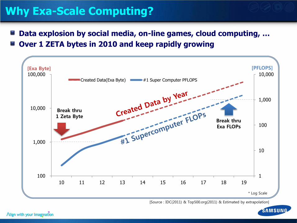
Why Exa-Scale Computing?
Data explosion by social media, on-line games, cloud computing, …
Over 1 ZETA bytes in 2010 and keep rapidly growing
1
10
100
1,000
10,000
100
1,000
10,000
100,000
10 11 12 13 14 15 16 17 18 19
Created Data(Exa Byte) #1 Super Computer PFLOPS
[Exa Byte] [PFLOPS]
[Source : IDC(2011) & Top500.org(2011) & Estimated by extrapolation]
* Log Scale
Break thru Exa FLOPs
Break thru 1 Zeta Byte

Memory Wall
Widening of the gap between CPU and Memory performance
• Memory becomes more important than ever
• Requires larger capacity, higher performance, and better power efficiency
0.0
0.1
1.0
10.0
100.0
1,000.0
10,000.0
100,000.0
1,000,000.0
10,000,000.0
100,000,000.0
1980 1985 1990 1995 2000 2003 2005 2010 2015
Effective CPU cycle time
CPU cycle time
SRAM access time
DRAM access time
Flash SSD access time
Disk seek time
[ns]
HDD
SSD
DRAM
SRAM
CPU
DRAM vs. CPU
Exa-Scale
Memory Capacity (System)
~10PB
Memory BW (Node)
0.5~1TB/s
Power (System)
~20MW
[Carnegie Mellon Univ. & Samsung Estimation]

Contents
1. Introduction
2. DRAM Requirements in Exa-Scale Computing
3. DRAM Technology Evolution & Challenges
4. DRAM Solution Consideration
5. SSD for Storage Solution
6. New Memory Technology : STT-MRAM
7. Summary

Memory Capacity/System Memory Capacity/Node DRAM Component Capacity
Capacity Requirements in Exa-Scale Computing
Requires more than 70x memory capacity
Peta-flops 20Peta-flops Exa-flops
100~200TB
>5x (~750TB)
>70x (~10PB)
Now
2~4GB
>4x (~16GB)
>32x (~128GB)
512Mb~1Gb
>2x (~2Gb)
>8x (~8Gb)
2018
[Source: “Memory systems for PetaFlop to ExaFlop class machines” by IBM, 2007 & 2010]
Memory Capacity Requirements
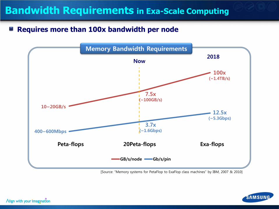
GB/s/node Gb/s/pin
Peta-flops 20Peta-flops Exa-flops
400~600Mbps
3.7x (~1.6Gbps)
12.5x (~5.3Gbps)
Now
10~20GB/s
7.5x (~100GB/s)
100x (~1.4TB/s)
Bandwidth Requirements in Exa-Scale Computing
Requires more than 100x bandwidth per node
2018
[Source: “Memory systems for PetaFlop to ExaFlop class machines” by IBM, 2007 & 2010]
Memory Bandwidth Requirements
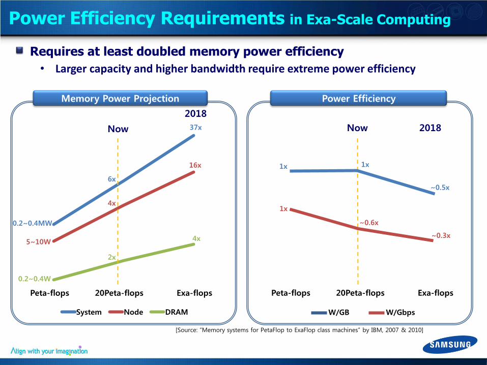
Power Efficiency Requirements in Exa-Scale Computing
Requires at least doubled memory power efficiency
• Larger capacity and higher bandwidth require extreme power efficiency
System Node DRAM
Peta-flops 20Peta-flops Exa-flops
Now
0.2~0.4MW
5~10W
0.2~0.4W
6x
4x
2x
37x
16x
4x
Now
1x 1x
~0.5x
1x
~0.6x
~0.3x
Peta-flops 20Peta-flops Exa-flops
[Source: “Memory systems for PetaFlop to ExaFlop class machines” by IBM, 2007 & 2010]
2018
2018
Memory Power Projection Power Efficiency
W/Gbps W/GB

Contents
1. Introduction
2. DRAM Requirements in Exa-Scale Computing
3. DRAM Technology Evolution & Challenges
4. DRAM Solution Consideration
5. SSD for Storage Solution
6. New Memory Technology : STT-MRAM
7. Summary

Memory Module Capacity Trend
Larger capacity mono die introduction is getting delayed
• Technology difficulty & tremendous investment
• Disruptive technology is necessary to increase module capacity more
[GB]
16
32
[Year]
64
* Highest Module Capacity with Mono-component
4Gb
8Gb @ 20nm Class
16Gb @ 10nm Class
2011 2015 2018
Subject to cost/energy efficiency, scaling, …

Performance Trend
[Mbps]
1333
1600
1866
2133
2400/2667
3200 Limitation by memory I/F & channel environment
Limitation by physical channel environment & stacking technology
3600
4200
Feeding data with enough BW will be the 1st Challenge for exa-scale Computing
DDR5(?) & New I/F(Optic)
DDR4
*Highest speed in that year
2011 2015 2018 [Year]
Subject to cost/energy efficiency, scaling, …

Channel Environment Challenge
Limitation of physical channel environment
• Validity of multi-drop bus architecture beyond DDR4 to support > 25.6GBps/Ch. ?
New approach for memory sub-system
• Differential signaling or serial link ?
• New bus architecture like point-to-point, daisy-chained, …
• New technology like optical I/O
DDR4 Post DDR4*
Speed/pin 1.6~3.2Gbps ~6.4Gbps
BW/Ch. ~25.6GB/s ~51.2GB/s
* Expectation

Memory Power Efficiency Trend
Aggressive process shrink provides better power efficiency and performance
20nm class 4Gb 1.35V can offer the most efficient power usage
50nm class DDR3 2Gb 1.5V
40nm class DDR3 2Gb 1.5V
30nm class DDR3 2Gb
1.35V
20nm class DDR3 4Gb
1.35V
20nm class DDR3 4Gb
1.25V*
Considered with an 8 hours active and 16 hours idle status in server
Green
DDR3-G2
Green
DDR3-G1
Source: Samsung Lab.
Green
DDR3-G3
Memory Power Consumption as measured in 96GB server
67% Savings
35% Savings
* Optional Solution
Technology Interface Density Voltage
65.3W
33.6W 21.8W 20.3W
42.8W
34% Savings
21% Savings

10.0
100.0
1000.0
Only Process Shrink
With New Technology
Efficiency improvement by process shrink only is limited
Additional technology aids to reduce the power consumption more
[Source : Samsung]
Traditional power reduction Needs more new technology
[mW/GB]
Power Efficiency Limitation Problem
CAGR(’10 – ’14) : -36%
CAGR(’14 – ’20) : -12%
CAGR (’14 – ’20) : -18%
40nm class 30nm class 20nm class 10nm class Sub 10nm class
Sub 1.0V
2011 2015 2018
TSV Optic I/O
* Log Scale
* Estimated in 8hr active and 16hr standby
- Considered speed and supply voltage by generation

Technology Scaling Challenges
DRAM is not free any more • Scaling approaches a theoretical limit
• Technology difficulty & large investment
Very difficult to achieve economical scaling
40nm class 30nm class 20nm class 10nm class Sub 10nm class
2011 2015 2018
Cost/bit
Investment/WF
Transition Period
Requires Close-Collaboration between All Parties: CPU, Memory, S/W, etc
Contents
1. Introduction
2. DRAM Requirements in Exa-Scale Computing
3. DRAM Technology Evolution & Challenges
4. DRAM Solution Consideration
5. SSD for Storage Solution
6. New Memory Technology : STT-MRAM
7. Summary

TSV(Through-Silicon Via)
TSV offers less power consumption and higher performance by hiding electrical loading
Still concern on cost, even if matured, intrinsic cost overhead exist…
Traditional RDIMM 3DS-TSV RDIMM
Power Comparison
☞ Merits 3DS-TSV consumes 17% lower power
17% Saving
* Measured by 32GB RDIMM @ 2DPC
TSV Conventional Stacking
Pros
• Short Interconnection (< ~50um) • Lower Profile • More # of Interconnects (>1000ea)
Low Cost & Matured Technology
Cons High Cost • Long Loop Wires • Higher Profiles • Limitations in # of Interconnects • Overhang

Optical Interface
Mainly has been utilized in long distant communication
Interface Power(I/O & Termination) getting dominant
• Memory sub-system is relatively short channel environment
• Potential to get ~60% better power efficiency over DDR3 interface
• Opportunity to expand # of slots and support high pin speed
• How to implement power efficient and low cost optical I/O solution?
40nm class 30nm class 20nm class
I/O Power & Termination RCD Power Core Power
29% 34% 40%
18% 21% 24%
53% 45% 36%
0
10
20
30
40
0 2 4 6 8 10 12
Bandwidth / pin (Gbps)
Pow
er
Cost
(mW
/Gbps)
DDR2 0.8Gbps
DDR3 1.6Gbps
XDR 3.2Gbps
GDDR55.0Gbps Optical
10Gbps
Optical GDDR5
DDR3 1.6Gbps
DDR2 0.8Gbps
XDR 3.2Gbps
Pow
er
Cost
[mW
/Gbps]
Bandwidth / pin[Gbps]
I/F power getting dominant Optical I/O : lower Power per B/W
* Source : Samsung
60%

Source: Hot chip 2011
Controller Offloading
Potential advantages by additional functionalities in logic die
• Distributed small scale computing
• Reduced controller complexity & increased performance
• Better system power efficiency with reduced data traffic
• Additional logic to enhance device reliability and DRAM scaling extension
• Supporting heterogeneous memories DDR3, DDR4, PRAM, Flash, MRAM etc.
Technology agnostic High speed Memory Interface
Offloading Control & Computing
TSV
Memory Cube
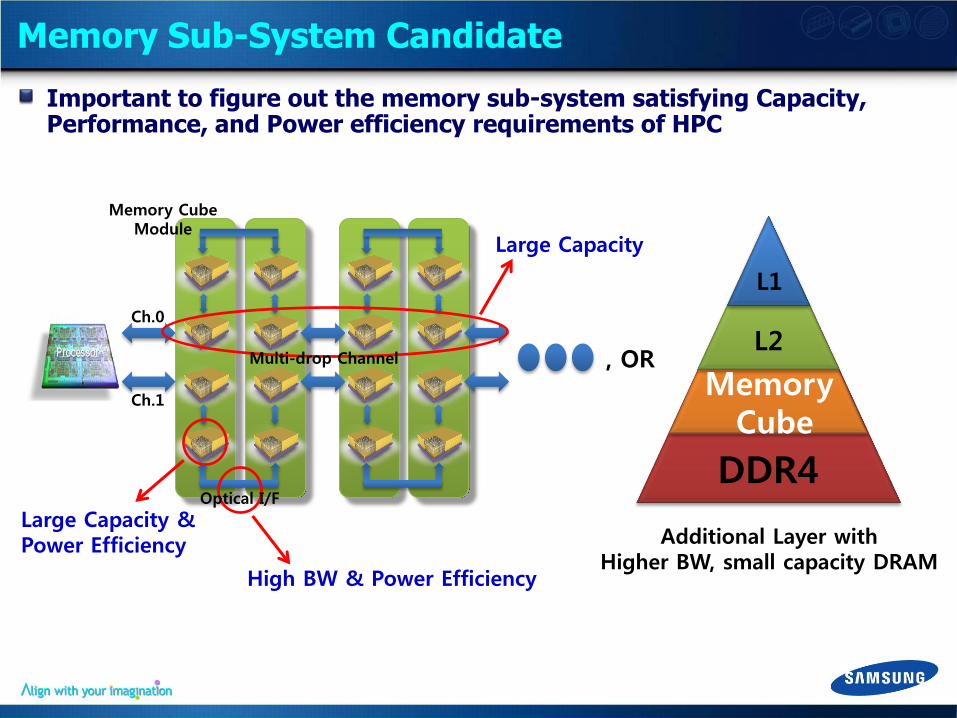
Memory Sub-System Candidate
Important to figure out the memory sub-system satisfying Capacity, Performance, and Power efficiency requirements of HPC
Ch.0
Ch.1
Memory Cube Module
Optical I/F
High BW & Power Efficiency
Multi-drop Channel
Large Capacity & Power Efficiency
Large Capacity
L1
L2
Memory Cube
DDR4
Additional Layer with Higher BW, small capacity DRAM
, OR
Contents
1. Introduction
2. DRAM Requirements in Exa-Scale Computing
3. DRAM Technology Evolution & Challenges
4. DRAM Solution Consideration
5. SSD for Storage Solution
6. New Memory Technology : STT-MRAM
7. Summary

The Performance Gap : Flash Is A Good Fit
Huge latency gap between memory and disk drive
• Only 1.3X mechanical access improvement in HDD for 13 years
• Flash storage is a good gap filler to minimize the distance
Latency Gap
Flash storage is a good
candidate to fill the gap
“I/O Memory Tier” (Typically 50us ~ 300us Latency)
Limiting System Performance
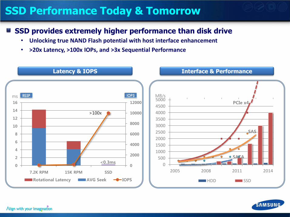
SSD Performance Today & Tomorrow
SSD provides extremely higher performance than disk drive
• Unlocking true NAND Flash potential with host interface enhancement
• >20x Latency, >100x IOPs, and >3x Sequential Performance
ms
0
2000
4000
6000
8000
10000
12000
0
2
4
6
8
10
12
14
16
7.2K RPM 15K RPM SSD
Rotational Latency AVG Seek IOPS
<0.3ms
Latency & IOPS
2004 2006 2008 2010 2012 2014 2016
0
500
1000
1500
2000
2500
3000
3500
4000
4500
5000
2005 2008 2011 2014
HDD SSD
SAS
SATA
MB/s
PCIe x4
Interface & Performance
>100x
Power Saving with SSD
Enhanced energy efficiency and smaller footprint through SSD
• Higher single device performance reduces number of drives
• A case study shows 73% power reduction with a half number of drives
[W]
2730 W
736 W
0
500
1000
1500
2000
2500
3000
HDD only HDDs+SSDs
Aggregated SAS
5% 200GB SSD 25ea. 95% 7.4K RPM 2TB SATA 48ea.
15K SAS
Tired Storage
7.5K SATA
100% 15K RPM 600GB SAS 167ea.
73% reduction/system Smaller footprint
(~ ½ number of drives )
Source : EMC, 2011 Storage Capacity: 100TB
Case Study
..… ..…

NAND Flash Innate Characteristics
Sop
his
tica
ted
NA
ND
Fla
sh
Man
age
me
nt
Tech
no
logy
High Performance & Reliable
SSD
• NAND characteristics
- No overwrite
- Page operation
but block erase
• NAND suffers from
- P/E cycle
- Data retention VS.
NAND flash management technique is different

Managing Endurance
Facing challenges to maintain P/E cycles with process shrink
• To extend SSD life time, it needs sophisticated HW & SW technologies
- Continued Evolution in Controller Technology
- Adaptive Management & Tuned NAND Flash
- Application Awareness
NAND Flash Endurance
10K
100K
2004 2008 2012
100K
50K ~100K
10K
5K
3K
1.5K
2016
MLC Endurance
SLC Endurance Shrink Rate Slows Down
Reliability Degrades
Performance Deteriorates
Years
SSD Requirement

How To Utilize SSD Value
Active collaboration is the key for SSD value capture in HPC
• SSD characteristics is too variant to be a generic solution for all storage needs
• Engineered systems allows to accelerate the benefits of flash while avoiding the pitfalls
Active Collaboration
NAND Flash Controller
F/W
Host System & Application
New Architecture, Algorithm, Software, File System, Application Dependant, Metadata, …
7.2K rpm, 15K rpm
From Simple Replacement To Transformation
Contents
1. Introduction
2. DRAM Requirements in Exa-Scale Computing
3. DRAM Technology Evolution & Challenges
4. DRAM Solution Consideration
5. SSD for Storage Solution
6. New Memory Technology : STT-MRAM
7. Summary

New Memory Technology : STT-MRAM
Non-volatility and comparable to DRAM
• Highly desired solution, but technology maturity?
Outer Better
Retention
Tech. Maturity
Speed (RD/WT)
Standby Power
Endurance Bit cost
(Scalability)
DRAM
STT-MRAM
STT-MRAM Cell Structure
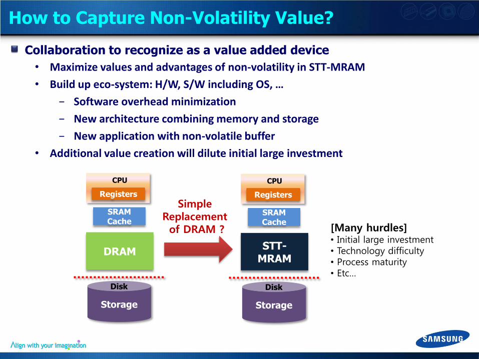
How to Capture Non-Volatility Value?
CPU
Registers
SRAM Cache
DRAM
Storage
Disk
CPU
Registers
SRAM Cache
STT-MRAM
Storage
Disk
Simple Replacement of DRAM ? [Many hurdles]
• Initial large investment • Technology difficulty • Process maturity • Etc…
Collaboration to recognize as a value added device
• Maximize values and advantages of non-volatility in STT-MRAM
• Build up eco-system: H/W, S/W including OS, …
− Software overhead minimization
− New architecture combining memory and storage
− New application with non-volatile buffer
• Additional value creation will dilute initial large investment

Contents
1. Introduction
2. DRAM Requirements in Exa-Scale Computing
3. DRAM Technology Evolution & Challenges
4. DRAM Solution Consideration
5. SSD for Storage Solution
6. New Memory Technology : STT-MRAM
7. Summary

Exa-Scale computing requires large capacity, high bandwidth, and power efficient memory sub-system
DRAM technology is getting difficult and expensive
A revolutionary and innovative memory solution is mandatory
• Continued scaling, TSV, Optical IO, Controller offloading, …
SSD is a good candidate for efficient storage system
• Very high performance and power efficient device
• Different characteristics require different optimization
Very high potential in STT-MRAM, but technology is not yet
Call to action for active and strong collaboration between all parties
Summary