ADSP-218x DSP Hardware Reference
468
ADSP-218x DSP Hardware Reference First Edition, February 2001 Part Number 82-002010-01 Analog Devices, Inc. Digital Signal Processor Division One Technology Way Norwood, Mass. 02062-9106 a
-
Upload
pranav-vaidik -
Category
Documents
-
view
49 -
download
2
Transcript of ADSP-218x DSP Hardware Reference

ADSP-218xDSP Hardware Reference
First Edition, February 2001
Part Number82-002010-01
Analog Devices, Inc.Digital Signal Processor DivisionOne Technology WayNorwood, Mass. 02062-9106 a

Copyright Information©1996–2001 Analog Devices, Inc., ALL RIGHTS RESERVED. This document may not be reproduced in any form without prior, express writ-ten consent from Analog Devices, Inc.
Printed in the USA.
DisclaimerAnalog Devices, Inc. reserves the right to change this product without prior notice. Information furnished by Analog Devices is believed to be accurate and reliable. However, no responsibility is assumed by Analog Devices for its use; nor for any infringement of patents or other rights of third parties which may result from its use. No license is granted by impli-cation or otherwise under the patent rights of Analog Devices, Inc.
Trademark and Service Mark NoticeThe Analog Devices logo, VisualDSP, VisualDSP++, the VisualDSP logo, VisualDSP++ logo, EZ-ICE, and EZ-LAB are registered trademarks; and, the White Mountain logo, Apex-ICE, Mountain-ICE, Moun-tain-ICE/WS, Summit-ICE, Trek-ICE, Vista-ICE, and The DSP Collaborative are trademarks of Analog Devices, Inc.
Microsoft and Windows are registered trademarks and Windows NT is a trademark of Microsoft Corporation.
Adobe and Acrobat are registered trademarks of Adobe Corporation.
All other brand and product names are trademarks or service marks of their respective owners.

CONTENTS
INTRODUCTION
Purpose ......................................................................................... 1-1
Audience ...................................................................................... 1-1
Overview ...................................................................................... 1-2
ADSP-218x Family Processors ................................................. 1-4
Functional Units ..................................................................... 1-6
Memory and System Interface .................................................. 1-9
Instruction Set ...................................................................... 1-10
DSP Performance .................................................................. 1-11
Core Architecture ........................................................................ 1-12
Computational Units ............................................................. 1-14
Address Generators and Program Sequencer ........................... 1-15
Buses ..................................................................................... 1-16
On-chip Peripherals .................................................................... 1-17
Serial Ports ............................................................................ 1-17
Timer .................................................................................... 1-17
DMA Ports ........................................................................... 1-18
ADSP-218x DSP Hardware Reference iii

CONTENTS
Development Tools ..................................................................... 1-19
Integrated Development Environment ................................... 1-19
Debugger .............................................................................. 1-20
Software Development Tools ................................................. 1-20
C Compiler and Assembler ............................................... 1-20
Linker and Loader ............................................................ 1-21
Hardware Development Tools ............................................... 1-21
EZ-KIT Lite ..................................................................... 1-21
EZ-ICE ............................................................................ 1-22
Third Party Products ............................................................. 1-22
Information Online .................................................................... 1-23
Customer Support ...................................................................... 1-24
Related Documents .................................................................... 1-24
Conventions ............................................................................... 1-25
COMPUTATIONAL UNITS
Overview ...................................................................................... 2-1
Binary String .......................................................................... 2-1
Unsigned Binary Numbers ...................................................... 2-2
Signed Numbers: Twos-Complement ....................................... 2-2
Fractional Representation: 1.15 ............................................... 2-2
ALU Arithmetic ...................................................................... 2-3
MAC Arithmetic ..................................................................... 2-4
Shifter Arithmetic ................................................................... 2-4
Arithmetic Formats Summary .................................................. 2-5
iv ADSP-218x DSP Hardware Reference

CONTENTS
Arithmetic Logic Unit (ALU) ........................................................ 2-7
ALU Structure ......................................................................... 2-8
Standard Functions ................................................................ 2-11
ALU Input/Output Registers ................................................. 2-12
Multiprecision Capability ...................................................... 2-13
ALU Saturation Mode ........................................................... 2-13
ALU Overflow Latch Mode ................................................... 2-14
Division ................................................................................ 2-14
ALU Status ............................................................................ 2-20
Multiplier Accumulator (MAC) ................................................... 2-20
MAC Structure ...................................................................... 2-21
MAC Operations ................................................................... 2-24
Standard Functions ........................................................... 2-24
Input Formats ................................................................... 2-27
MAC Input/Output Registers ............................................ 2-28
MR Register Operation ..................................................... 2-28
MAC Overflow And Saturation ......................................... 2-29
Rounding Mode ................................................................ 2-30
Biased Rounding ............................................................... 2-31
ADSP-218x DSP Hardware Reference v

CONTENTS
Barrel Shifter .............................................................................. 2-32
Shifter Structure .................................................................... 2-32
Shifter Operations ................................................................. 2-40
Shifter Input/Output Registers .......................................... 2-41
Derive Block Exponent ..................................................... 2-41
Immediate Shifts .............................................................. 2-42
Denormalize ..................................................................... 2-44
Normalize ........................................................................ 2-45
PROGRAM SEQUENCER
Overview ...................................................................................... 3-1
Program Sequencer Structure ........................................................ 3-2
Next Address Select Logic ........................................................ 3-3
Program Counter Register and Stack ........................................ 3-4
Loop Counter Register and Stack ............................................ 3-5
Loop Comparator and Stack .................................................... 3-6
Program Control Instructions ..................................................... 3-11
JUMP Instruction ................................................................. 3-11
Direct JUMP Instructions ................................................. 3-11
Register Indirect JUMP Instructions ................................. 3-11
CALL Instruction ................................................................. 3-13
DO UNTIL Loops ................................................................ 3-13
IDLE Instruction .................................................................. 3-15
Slow IDLE Instruction ..................................................... 3-15
vi ADSP-218x DSP Hardware Reference

CONTENTS
Interrupts ................................................................................... 3-16
Interrupt Servicing Sequence ................................................. 3-18
Configuring Interrupts .......................................................... 3-19
Interrupt Control Register ................................................. 3-20
Interrupt Mask Register .................................................... 3-20
Global Enable/Disable for Interrupts ................................. 3-23
Interrupt Force and Clear Register ..................................... 3-23
Interrupt Latency .............................................................. 3-24
Status Registers and Status Stack .................................................. 3-26
Arithmetic Status Register ...................................................... 3-27
Stack Status Register .............................................................. 3-28
Mode Status Register ............................................................. 3-30
Conditional Instructions ............................................................. 3-33
TOPPCSTACK Instruction ......................................................... 3-34
TOPPCSTACK Restrictions .................................................. 3-37
DATA ADDRESS GENERATORS
Overview ...................................................................................... 4-1
Data Address Generators (DAGs) .................................................. 4-1
DAG Registers .............................................................................. 4-2
Indirect Addressing .................................................................. 4-4
Linear Indirect Addressing ................................................... 4-4
Modulo Addressing (Circular Buffers) ...................................... 4-5
ADSP-218x DSP Hardware Reference vii

Calculating the Base Address ................................................... 4-6
Circular Buffer Base Address Example 1 .............................. 4-6
Circular Buffer Base Address Example 2 .............................. 4-7
Circular Buffer Operation Example 1 .................................. 4-7
Circular Buffer Operation Example 2 .................................. 4-7
Bit-Reverse Addressing ............................................................ 4-8
Programming Data Accesses .......................................................... 4-9
Variables and Arrays ................................................................ 4-9
Circular Buffers .................................................................... 4-10
PMD-DMD Bus Exchange ......................................................... 4-11
PMD-DMD Bus Exchange Structure ..................................... 4-11
Using DAGs with Hardware Overlays ......................................... 4-14
SERIAL PORTS
Overview ...................................................................................... 5-1
Basic Description .......................................................................... 5-1
Interrupts ............................................................................... 5-5
Operation ............................................................................... 5-5
SPORT Programming ................................................................... 5-6
Configuration ......................................................................... 5-6
Receiving and Transmitting Data ............................................. 5-9
viii ADSP-218x DSP Hardware Reference

CONTENTS
SPORT Enable ........................................................................... 5-10
Serial Clocks ............................................................................... 5-11
Word Length .............................................................................. 5-13
Word Framing Options ............................................................... 5-14
Frame Synchronization .......................................................... 5-14
Frame Synchronization Signal Source ..................................... 5-15
Normal and Alternate Framing Modes ................................... 5-17
Active High or Active Low ..................................................... 5-18
Configuration Example ............................................................... 5-19
Timing Examples ........................................................................ 5-21
Companding and Data Format .................................................... 5-28
Companding Operation Example ........................................... 5-29
Contention for Companding Hardware .................................. 5-30
Companding Internal Data .................................................... 5-31
Autobuffering ............................................................................. 5-32
Autobuffer Control Register ................................................... 5-34
Serial Port Autobuffering on the ADSP-2187/2188/2189 Processors .......................................................................... 5-35
Autobuffering Example .......................................................... 5-36
ADSP-218x DSP Hardware Reference ix

Multichannel Function ............................................................... 5-38
Multichannel Setup ............................................................... 5-39
Multichannel Operation ........................................................ 5-41
SPORT Timing Considerations .................................................. 5-44
Companding Delay ............................................................... 5-44
Clock Synchronization Delay ................................................ 5-44
Startup Timing ................................................................. 5-45
Internally Generated Frame Sync Timing ............................... 5-45
Transmit Interrupt Timing .................................................... 5-47
Receive Interrupt Timing ...................................................... 5-48
Interrupt and Autobuffer Synchronization ............................. 5-49
Instruction Completion Latencies .......................................... 5-50
Interrupt and Autobuffer Service Example ............................. 5-51
Receive Companding Latency ................................................ 5-52
Interrupts with Autobuffering Enabled .................................. 5-53
Unusual Complications ......................................................... 5-54
Serial Port Startup Issues ............................................................. 5-55
Gated Serial Clocks ............................................................... 5-55
Ringing and Overshoot on Serial Clock Pins .......................... 5-57
Multi-Cycle Frame Sync Pulse ............................................... 5-57
x ADSP-218x DSP Hardware Reference

CONTENTS
TIMER
Overview ...................................................................................... 6-1
Timer Architecture ........................................................................ 6-2
Resolution .................................................................................... 6-4
Timer Operation ........................................................................... 6-4
Enabling the Timer ....................................................................... 6-6
SYSTEM INTERFACE
Overview ...................................................................................... 7-1
Pin Descriptions ........................................................................... 7-1
Pin Descriptions for 128-LQFP Package Processors .................. 7-3
Pin Descriptions for 100-LQFP Package Processors .................. 7-7
Common-Mode Pins ........................................................... 7-9
Memory Mode Pins .......................................................... 7-12
Active or Passive Mode Pin Configuration ......................... 7-13
Terminating Unused Pins .................................................. 7-14
Recommendations for Unused Pins ................................... 7-18
Clock Signals .............................................................................. 7-19
Synchronization Delay ........................................................... 7-22
1/2x Clock Considerations .................................................... 7-22
Resetting the Processor ................................................................ 7-23
Software-Forced Rebooting ......................................................... 7-24
Register Values for BDMA Booting ........................................ 7-30
ADSP-218x DSP Hardware Reference xi

External Interrupts ..................................................................... 7-31
Interrupt Sensitivity .............................................................. 7-32
Flag Pins .................................................................................... 7-33
Powerup Issues ........................................................................... 7-35
Powerup Sequence ................................................................ 7-36
Power Supplies ...................................................................... 7-37
Dual Supply Example ....................................................... 7-38
Reset Generators ................................................................... 7-40
Powerdown ................................................................................. 7-43
Powerdown Control .............................................................. 7-44
Entering Powerdown ............................................................. 7-45
Exiting Powerdown ............................................................... 7-46
Ending Powerdown with the Powerdown Pin ..................... 7-46
Ending Powerdown with the RESET Pin ........................... 7-47
Startup Time after Powerdown .............................................. 7-48
Systems Using an External TTL/CMOS Clock .................. 7-48
Systems Using a Crystal and the Internal Oscillator ........... 7-49
Processor Operation During Powerdown ................................ 7-51
Interrupts and Flags .......................................................... 7-51
SPORTs ........................................................................... 7-51
IDMA Port During Powerdown ........................................ 7-53
BDMA Port During Powerdown ....................................... 7-53
Conditions for Lowest Power Consumption ........................... 7-54
PWDACK Pin ...................................................................... 7-57
xii ADSP-218x DSP Hardware Reference
CONTENTS
Using Powerdown as a Non-Maskable Interrupt ..................... 7-59
Bus Request/Grant ...................................................................... 7-59
Target System Hardware .............................................................. 7-62
Target Board Connector for EZ-ICE Probe ............................ 7-62
Using Mode Pins with RESET and ERESET Signals .......... 7-64
Bus Request Signal ................................................................ 7-65
Memory Select Signals ........................................................... 7-66
Decoupling Capacitors .......................................................... 7-66
RESET Signal ....................................................................... 7-67
PCB Board ............................................................................ 7-67
EZ-ICE Powerup Procedure ................................................... 7-68
Other Considerations ............................................................ 7-68
Recommended Reading ......................................................... 7-69
MEMORY INTERFACE
Overview ...................................................................................... 8-1
Program Memory and Data Memory ........................................ 8-1
Byte Memory Space ................................................................. 8-2
I/O Memory Space .................................................................. 8-2
Memory Buses ......................................................................... 8-2
External Memory Spaces .......................................................... 8-3
Composite Memory Select ....................................................... 8-3
External Overlay Memory ........................................................ 8-3
Internal Direct Memory Access Port ......................................... 8-4
Memory Modes ....................................................................... 8-4
ADSP-218x DSP Hardware Reference xiii

Memory Interfaces ........................................................................ 8-5
Program Memory Interface ...................................................... 8-9
Data Memory Interface ......................................................... 8-12
Byte Memory Interface .......................................................... 8-15
I/O Memory Space ................................................................ 8-16
Composite Memory Select ..................................................... 8-18
CMS Signal as Chip Select for 32 K x 8-Bit SRAMs .......... 8-20
BMS Disable .................................................................... 8-21
Memory Interface Modes ............................................................ 8-23
Full Memory Mode ............................................................... 8-23
Host Memory Mode .............................................................. 8-24
Accessing Peripherals ........................................................ 8-24
Byte Memory Accesses ...................................................... 8-25
Memory Interface Pins .......................................................... 8-26
DMA PORTS
Overview ...................................................................................... 9-1
BDMA Port .................................................................................. 9-2
BDMA Port Functional Description ........................................ 9-4
BDMA Control Registers ........................................................ 9-5
Byte Memory Word Formats ................................................. 9-14
BDMA Booting .................................................................... 9-15
Development Software Features for BDMA Booting .......... 9-20
xiv ADSP-218x DSP Hardware Reference

CONTENTS
IDMA Port ................................................................................. 9-21
IDMA Port Pin Summary ...................................................... 9-22
DMA Port Functional Description ......................................... 9-28
Modifying Control Registers for IDMA ................................. 9-31
IDMA Timing ....................................................................... 9-32
Address Latch Cycle .......................................................... 9-33
Overlay Latch Cycle .......................................................... 9-34
Long Read Cycle ............................................................... 9-35
Short Read Cycle .............................................................. 9-37
IDMA Read—Short Read Only Mode ............................... 9-40
Long Write Cycle .............................................................. 9-41
Short Write Cycle .............................................................. 9-44
Boot Loading through the IDMA Port ................................... 9-46
DMA Cycle Stealing, Hold Offs, and IACK Acknowledge ...... 9-47
Priority Chain ................................................................... 9-49
HARDWARE INTERFACING AND EXAMPLES
Overview .................................................................................... 10-1
Interfacing to DSP Processors ...................................................... 10-1
Parallel Interfacing to DSP Processors .................................... 10-2
Reading Data from Memory-Mapped ADCs ...................... 10-2
Writing Data to Memory-Mapped DACs ......................... 10-10
Serial Interfacing to DSP Processors ..................................... 10-16
Serial ADC to DSP Interface ........................................... 10-19
Serial DAC to DSP Interface ........................................... 10-23
ADSP-218x DSP Hardware Reference xv

Interfacing I/O Ports, Analog Front Ends, and Codecs ......... 10-25
High-Speed Interfacing ....................................................... 10-29
DSP System Interface .......................................................... 10-31
Interfacing Examples ................................................................ 10-32
Serial Port to Codec Interface .............................................. 10-32
Serial Port to ADC Interface ................................................ 10-34
ADSP-218x DSP to AD7475/95 ADC Interface ............. 10-34
ADSP-218x DSP to AD7888 ADC interface ................... 10-36
Parallel Port to ADC Interface ............................................. 10-38
Serial Port to DAC Interface ................................................ 10-40
IDMA Interface to a Host Processor .................................... 10-42
IDMA Operation ........................................................... 10-42
Host Interface Hardware Design ..................................... 10-45
System Design Issues ...................................................... 10-49
Advanced Topics ............................................................. 10-58
References ................................................................................ 10-59
NUMERIC FORMATS
Overview ...................................................................................... A-1
Unsigned or Signed: Twos-Complement Format ............................ A-1
Integer or Fractional Format ......................................................... A-2
xvi ADSP-218x DSP Hardware Reference

CONTENTS
Binary Multiplication ................................................................... A-5
Fractional Mode and Integer Mode ......................................... A-6
Block Floating-Point Format ........................................................ A-7
CONTROL/STATUS REGISTERS
Overview ..................................................................................... B-1
Memory-Mapped Registers ........................................................... B-3
Non-Memory Mapped Registers ................................................. B-17
ADVANCED PRODUCT FEATURES
Overview ..................................................................................... C-1
INDEX
ADSP-218x DSP Hardware Reference xvii

xviii ADSP-218x DSP Hardware Reference

1 INTRODUCTIONFigure 1-0.
Table 1-0.
Listing 1-0.
PurposeThe ADSP-218x DSP Hardware Reference provides architectural and design information about the ADSP-218x family of digital signal proces-sors (DSPs). The architectural descriptions cover functional blocks, busses, and ports. The ADSP-218x DSP Instruction Set Reference manual covers programming information. The ADSP-218x data sheets for each member of the family cover timing, electrical, and packaging specifica-tions, as well as, many other topics related to the features and design of the specific processor.
AudienceThis manual is developed primarily for DSP designers and programmers. The manual assumes that the audience is familiar with signal processing concepts and has a working knowledge of microcomputer technology and DSP-related mathematics.
ADSP-218x DSP Hardware Reference 1-1
Overview
OverviewThe ADSP-218x family is a collection of programmable single-chip microprocessors that share a common base architecture optimized for dig-ital signal processing (DSP) and other high-speed numeric processing applications.
These processors can be used in such diverse applications as:
• Speaker phones
• Smart phones
• Smart-card readers
• POS terminals
• Digital speech interpolation
• Video conferencing
• Data encryption
• ISDN modems
• Pattern matching
• Global positioning
• Navigation
1-2 ADSP-218x DSP Hardware Reference

Introduction
The ADSP-218x family processor architecture includes the following features:
• Three computational units
• Two data address generators
• A program sequencer
• Two bidirectional serial ports
• A 16-bit internal DMA port
• A byte DMA port
• A programmable timer
• Flag I/O
• Extensive interrupt capabilities
• On-chip Program and Data Memory
The ADSP-218x family members differ principally in the following:
• Amount of on-chip memory (Program and Data RAM)
• Supply voltage
• Instruction processing rate (MIPS)
• External memory interface modes
This manual provides the information necessary to understand and evalu-ate the processors’ architecture, and to determine which device best meets your needs for a particular application. Together with the data sheets describing the individual devices, this manual provides all the information required to design a DSP system.
ADSP-218x DSP Hardware Reference 1-3

Overview
ADSP-218x Family ProcessorsThe ADSP-218x family includes 18 members. Table 1-1 lists the members and identifies their basic distinguishing features. For additional features, see Chapter C, “Advanced Product Features.”
Table 1-1. ADSP-218x Family Processors
Processor Package Pro-gramRAM
DataRAM
MIPS(Max)
TypicalCore
Supply Voltage
Typical I/O
SupplyVoltage
MaximumInput
Voltage
ADSP-2181 128-LQFP
128-MQFP
16 K 16 K 40 5.0 Supply + .5
ADSP-2183 128-LQFP
144-miniBGA
16 K 16 K 52 3.3 Supply + .5
ADSP-2184 100-LQFP 4 K 4 K 40 5.0 Supply + .5
ADSP-2184L1 100-LQFP 4 K 4 K 40 3.3 Supply + .5
ADSP-2184N3 100-LQFP
144-miniBGA
4 K 4 K 80 1.8 1.8, 2.5 or 3.3
3.6
ADSP-2185 100-LQFP 16 K 16 K 33 5.0 Supply + .5
ADSP-2185L1 100-LQFP
144-miniBGA
16 K 16 K 52 3.3 Supply + .5
ADSP-2185M2 100-LQFP
144-miniBGA
16 K 16 K 75 2.5 2.5 or 3.3 3.6
ADSP-2185N3 100-LQFP
144-miniBGA
16 K 16 K 80 1.8 1.8, 2.5 or 3.3
3.6
1-4 ADSP-218x DSP Hardware Reference

Introduction
ADSP-2186 100-LQFP
144-miniBGA
8 K 8 K 40 5.0 Supply + .5
ADSP-2186L1 100-LQFP
144-miniBGA
8 K 8 K 40 3.3 Supply + .5
ADSP-2186M2 100-LQFP
144-miniBGA
8 K 8 K 75 2.5 2.5 or 3.3 3.6
ADSP-2186N3 100-LQFP
144-miniBGA
8 K 8 K 80 1.8 1.8, 2.5 or 3.3
3.6
ADSP-2187L1 100-LQFP 32 K 32 K 52 3.3 Supply + .5
ADSP-2187N3 100-LQFP
144-miniBGA
32 K 32 K 80 1.8 1.8, 2.5 or 3.3
3.6
ADSP-2188M2 100-LQFP
144-miniBGA
48 K 56 K 75 2.5 2.5 or 3.3 3.6
ADSP-2188N3 100-LQFP
144-miniBGA
48 K 56 K 80 1.8 1.8, 2.5 or 3.3
3.6
Table 1-1. ADSP-218x Family Processors (Cont’d)
Processor Package Pro-gramRAM
DataRAM
MIPS(Max)
TypicalCore
Supply Voltage
Typical I/O
SupplyVoltage
MaximumInput
Voltage
ADSP-218x DSP Hardware Reference 1-5

Overview
Functional UnitsThe ADSP-218x architecture includes the following main functional units:
• Computational Units—Every processor in the ADSP-218x family contains three independent, full-function computational units: an arithmetic/logic unit (ALU), a multiplier/accumulator (MAC) and a barrel shifter. The computational units process 16-bit data directly and also provide hardware support for multiprecision computa-tions.
ADSP-2189M2 100-LQFP
144-miniBGA
32 K 48 K 75 2.5 2.5 or 3.3 3.6
ADSP-2189N3 100-LQFP
144-miniBGA
32 K 48 K 80 1.8 1.8, 2.5 or 3.3
3.6
1 L indicates that the processor operates at 3.3 V. These processors are not tolerant to 5 V inputs.2 M indicates that the processor core operates at 2.5 V and that the external I/O can operate
at 2.5 V or 3.3 V. The external I/O is tolerant to up to 3.6 V inputs with a supply voltage of 2.5 V or 3.3 V. However, it is not tolerant to 5 V inputs.
3 N indicates that the processor core operates at 1.8 V and that the external I/O can operate at 1.8 V, 2.5 V or 3.3 V. The external I/O is tolerant to up to 3.6 V inputs with a supply voltage of 1.8 V, 2.5 V or 3.3 V. However, it is not tolerant to 5 V inputs.
Table 1-1. ADSP-218x Family Processors (Cont’d)
Processor Package Pro-gramRAM
DataRAM
MIPS(Max)
TypicalCore
Supply Voltage
Typical I/O
SupplyVoltage
MaximumInput
Voltage
1-6 ADSP-218x DSP Hardware Reference

Introduction
• Data Address Generators & Program Sequencer—Two dedicated address generators and a program sequencer supply addresses for on-chip or external memory access. The sequencer supports sin-gle-cycle conditional branching and executes program loops with zero overhead. Dual data address generators allow the processor to generate simultaneous addresses for dual operand fetches. Together the sequencer and data address generators keep the com-putational units continuously working, maximizing throughput.
• Memory—The ADSP-218x family uses a modified Harvard archi-tecture in which Data Memory stores data and Program Memory stores both instructions and data. All ADSP-218x family processors contain on-chip RAM that comprises a portion of the Program Memory space and Data Memory space. (Program Memory and Data Memory are directly addressable off-chip.) The speed of the on-chip memory allows the processor to fetch two operands (one from Data Memory and one from Program Memory) and an instruction (from Program Memory) in a single cycle.
• Serial Ports—The serial ports (SPORTs) provide a complete serial interface with hardware companding for data compression and expansion. Both µ-law and A-law companding are supported. The SPORTs interface easily and directly to a wide variety of popular serial devices. Each SPORT can generate a programmable internal clock or accept an external clock. SPORT0 includes a multichannel option.
• Timer—A programmable timer/counter with 8-bit prescaler pro-vides periodic interrupt generation.
ADSP-218x DSP Hardware Reference 1-7

Overview
• DMA Ports—The Internal DMA Port (IDMA) and Byte DMA Port (BDMA) in the ADSP-218x processors allow efficient data transfers to and from internal memory. The IDMA port is a slave port inter-face that has a 16-bit multiplexed address and data bus, which also supports 24-bit Program Memory accesses. The IDMA port is com-pletely asynchronous and can be written to while the ADSP-218x is operating at full speed. The Byte Memory DMA port is a master port that allows boot loading and storing of program instructions and data at or during runtime.
The ADSP-218x family architecture exhibits a high degree of parallelism, tailored to DSP requirements. In a single cycle, any device in the family can:
• Generate the next program address
• Fetch the next instruction
• Perform one or two data moves
• Update one or two data address pointers
• Perform a computation
In that same cycle, processors can also:
• Receive and/or transmit data through the serial ports
• Receive or transmit data through the internal DMA port
• Receive or transmit data via through byte DMA port
• Decrement timer
1-8 ADSP-218x DSP Hardware Reference

Introduction
Memory and System InterfaceIn each ADSP-218x processor, five on-chip buses connect internal mem-ory with the other functional units:
• Data Memory Address bus (14-bits)
• Data Memory Data bus (16-bits)
• Program Memory Address bus (14-bits)
• Program Memory Data bus (24-bits)
A single external address bus (14-bits) and a single external data bus (24-bits) are extended off-chip; these buses can be used for either Program or Data Memory accesses.
All ADSP-218x processors (except for the ADSP-2181 and ADSP-2183 processors) can be configured in either a Host Mode or a Full Memory Mode. In Host Mode, each processor has an Internal DMA (IDMA) port for connection to external host systems. The IDMA port provides trans-parent, direct access to the DSP’s on-chip Program and Data RAM. Since the ADSP-2181and ADSP-2183 processors have complete address, data, and IDMA busses, these two processors provide both IDMA and BDMA functionality concurrently, giving you greater system functionality with-out additional external logic.
In Full Memory Mode, the ADSP-218x processors have complete use of the external address and data busses. In this mode, the processors behave in exactly the same manner as the ADSP-2181 and ADSP-2183 processor with the IDMA port removed.
An interface to low cost byte-wide memory is provided by the Byte DMA port (BDMA) port. The BDMA port is bidirectional and can directly address up to four megabytes of external RAM or ROM for off-chip stor-age of program overlays or data tables.
ADSP-218x DSP Hardware Reference 1-9

Overview
Boot circuitry provides for loading on-chip Program Memory automati-cally after reset. This can be done through the BDMA port. Multiple programs can be selected and loaded with no additional hardware.
External devices can gain control of the processor’s buses with the bus request and bus grant signals (BR, BG). The ADSP-218x processors can continue running while the buses are granted to another device (when Go mode is enabled for the processor core) as long as an external memory operation is not required.
The ADSP-218x processors support memory-mapped peripherals with programmable wait state generation through a dedicated 2048 location I/O Memory space.
All ADSP-218x family processors operate in the same manner in their response to interrupts. The program sequencer allows the processor to respond with minimum latency. Interrupts can be nested with no addi-tional latency. External interrupts can be configured as edge- or level-sensitive. Internal interrupts can be generated from the timer, the host interface port, the serial ports, and the BDMA port.
Instruction SetThe ADSP-218x family shares a single unified instruction set designed for upward compatibility with higher-integration devices.
The ADSP-218x family instruction set provides flexible data moves. Mul-tifunction instructions combine one or more data moves with a computation. Every instruction can be executed in a single processor cycle. The assembly language uses an algebraic syntax for readability and ease of coding. A comprehensive set of software and hardware tools sup-ports program development. The instruction set is detailed in the ADSP-218x DSP Instruction Set Reference.
1-10 ADSP-218x DSP Hardware Reference

Introduction
DSP PerformanceSignal processing applications make special performance demands which distinguish DSP architectures from other microprocessor and microcon-troller architectures. Not only must instruction execution be fast, but DSPs must also perform well in each of the following areas:
• Fast and Flexible Arithmetic—The ADSP-218x family base architec-ture provides single-cycle computation for multiplication, multipli-cation with accumulation, arbitrary amounts of shifting, and standard arithmetic and logical operations. In addition, the arith-metic units allow for any sequence of computations so that a given DSP algorithm can be executed without being reformulated.
• Extended Dynamic Range—Extended sums-of-products, common in DSP algorithms, are supported in the multiply/accumulate units of the ADSP-218x family. A 40-bit accumulator provides eight bits of protection against overflow in successive additions to ensure that no loss of data or range occurs; 256 overflows would have to occur before any data is lost. Special instructions are provided for imple-menting block floating-point scaling of data.
• Single-Cycle Fetch of Two Operands—In extended sums-of-products calculations, two operands are needed on each cycle to feed the cal-culation. All members of the ADSP-218x family are able to sustain two-operand data throughput, whether the data is stored on-chip or off.
• Hardware Circular Buffers—A large class of DSP algorithms, includ-ing digital filters, requires circular data buffers. The ADSP-218x family base architecture includes hardware to handle address pointer wraparound, simplifying the implementation of circular buffers both on- and off-chip, and reducing overhead (thereby improving performance).
ADSP-218x DSP Hardware Reference 1-11

Core Architecture
• Zero-Overhead Looping and Branching—DSP algorithms are repeti-tive and are most logically expressed as loops. The program sequencer in the ADSP-218x family supports looped code with zero overhead, combining excellent performance with the clearest pro-gram structure. Likewise, there are no overhead penalties for condi-tional branches.
Core ArchitectureThis section gives a summary of the ADSP-218x family core architecture. Each component of the core architecture is described in detail in this man-ual. The following list identifies the ADSP-218x family’s core architectural components and specifies the chapters that cover each component:
• Arithmetic/logic unit (ALU)—Chapter 2, Computational Units
• Multiplier/accumulator (MAC)—Chapter 2, Computational Units
• Barrel shifter—Chapter 2, Computational Units
• Program sequencer—Chapter 3, Program Sequencer
• Status registers and stacks—Chapter 3, Program Sequencer
• Data Address generators (DAGs)—Chapter 4, Data Address Gener-ators
• PMD-DMD bus exchange (PX registers)—Chapter 4, Data Address Generators
1-12 ADSP-218x DSP Hardware Reference

Introduction
Figure 1-1 shows the ADSP-218x family core architecture. The sections that follow provide a brief summary of each core unit.
INPUT REGS
OUTPUT REGS
SHIFTER
INPUT REGS
OUTPUT REGS
ALU
INPUT REGS
OUTPUT REGS
MAC
R BUS 16
DMD BUS
PMD BUS
DATAADDRESS
GENERATOR#2
DATAADDRESS
GENERATOR#1
DMA BUS
PMA BUS14
14
24
16
PROGRAMSEQUENCER
Figure 1-1. Core Architecture
ADSP-218x DSP Hardware Reference 1-13

Core Architecture
Computational UnitsEvery processor in the ADSP-218x family contains three independent, full-function computational units: an arithmetic/logic unit (ALU), a mul-tiplier/accumulator (MAC) and a barrel shifter. The computation units process 16-bit data directly and provide hardware support for multipreci-sion computation as well.
The ALU performs a standard set of arithmetic and logic operations in addition to division primitives. The MAC performs single-cycle multiply, multiply/add and multiply/subtract operations. The shifter performs logi-cal and arithmetic shifts, normalization, denormalization, and derive-exponent operations. The shifter implements numeric format con-trol including multiword floating-point representations. The computational units are arranged side-by-side, instead of serially, so that the output of any unit may be the input of any unit on the next cycle. The internal result (R) bus directly connects the computational units to make this possible.
All three units contain input and output registers that are accessible from the internal Data Memory data (DMD) bus. Computational operations generally take their operands from input registers and load the result into an output register. The registers act as a stopover point for data between memory and the computational circuitry. This feature introduces one level of pipelining on input and one level on output. The R bus allows the result of a previous computation to be used directly as the input to another computation. This avoids excessive pipeline delays when a series of different operations are performed.
1-14 ADSP-218x DSP Hardware Reference
Introduction
Address Generators and Program SequencerTwo dedicated data address generators and a powerful program sequencer ensure efficient use of the computational units. The data address genera-tors (DAGs) provide memory addresses when memory data is transferred to or from the input or output registers. Each DAG keeps track of up to four address pointers. When a pointer is used for indirect addressing, it is post-modified by a value in a specified register. With two independent DAGs, the processor can generate two addresses simultaneously for dual operand fetches.
A length value may be associated with each pointer to implement auto-matic modulo addressing for circular buffers. (The circular buffer feature is also used by the serial ports for automatic data transfers. Refer to the Chapter 5, “Serial Ports.” for additional information.)
! For linear buffers, the length value must be set to zero.
DAG1 can supply addresses to Data Memory only; DAG2 can supply addresses to either Data Memory or Program Memory. When the appro-priate mode bit is set in the mode status register (MSTAT), the output address of DAG1 is bit-reversed before being driven onto the address bus. This feature facilitates addressing in radix-2 Fast Fourier Transform (FFT) algorithms.
The program sequencer supplies instruction addresses to the Program Memory. The sequencer is driven by the instruction register, which holds the currently executing instruction. The instruction register introduces a single level of pipelining into the program flow. Instructions are fetched and loaded into the instruction register during one processor cycle, and executed during the following cycle while the next instruction is prefetched. To minimize overhead cycles, the sequencer supports condi-tional jumps, subroutine calls and returns in a single cycle. With an internal loop counter and loop stack, the processor executes looped code with zero overhead. No explicit jump instructions are required to loop.
ADSP-218x DSP Hardware Reference 1-15
Core Architecture
BusesThe processors have five internal buses:
• Program Memory Address (PMA) and Data Memory Address (DMA) buses— Used internally for the addresses associated with Program and Data Memory.
• Program Memory Data (PMD) and Data Memory Data (DMD) buses — Used for the data associated with memory spaces. These buses are multiplexed into a single external address bus and a single external data bus; the BMS, DMS and PMS signals select the different address spaces.
• Result (R) bus—Transfers intermediate results directly between the various computational units.
The PMA bus is 14 bits wide allowing direct access of up to 16 K words of mixed instruction code and data. The PMD bus is 24 bits wide to accom-modate the 24-bit instruction width.
The DMA bus is 14 bits wide allowing direct access of up to 16 K words of data. The Data Memory data (DMD) bus is 16 bits wide. The DMD bus provides a path for the contents of any register in the processor to be transferred to any other register or to any Data Memory location in a sin-gle cycle. The Data Memory address comes from two sources: an absolute value specified in the instruction code (direct addressing) or the output of a data address generator (indirect addressing). Only indirect addressing is supported for data fetches from Program Memory.
The Program Memory data (PMD) bus can also be used to transfer data to and from the computational units through direct paths or via the PMD-DMD bus exchange unit. The PMD-DMD bus exchange unit per-mits data to be passed from one bus to the other. It contains hardware to overcome the 8-bit width discrepancy between the two buses, when necessary.
1-16 ADSP-218x DSP Hardware Reference

Introduction
On-chip PeripheralsThis section describes the additional functional units which are included in the ADSP-218x family processors.
Serial PortsThe ADSP-218x processors have two bidirectional, double-buffered serial ports (SPORTs) for serial communications. The SPORTs are synchronous and use framing signals to control data flow. Each SPORT can generate its serial clock internally or use an external clock. The framing sync signals may be generated internally or by an external device. Word lengths may vary from three to sixteen bits. One serial port, SPORT0, has a multi-channel capability that allows the receiving or transmitting of arbitrary data words from a 24-word or 32-word bitstream. The other serial port, SPORT1, may optionally be configured as two additional external inter-rupt pins (IRQ1 and IRQ0)and the Flag Out (FO) and Flag In (FI) pins.
TimerThe programmable interval timer provides periodic interrupt generation. An 8-bit prescaler register allows the timer to decrement a 16-bit count register over a range from each cycle to every 256 cycles. An interrupt is generated when this count register decrements to zero. The count register is automatically reloaded from a 16-bit period register after the timer interrupt is generated; the count resumes immediately.
ADSP-218x DSP Hardware Reference 1-17

On-chip Peripherals
DMA PortsThe ADSP-218x contains two DMA ports, an Internal DMA (IDMA) port and a Byte DMA (BDMA) port. The IDMA port provides an effi-cient means of communication between a host system and the DSP. The port is used to access the on-chip Program Memory and Data Memory of the DSP with only one cycle per word of overhead. The IDMA port has a 16-bit multiplexed address and data bus and supports 24-bit Program Memory. The IDMA port is completely asynchronous and can be written to while an ADSP-218x family processor is operating at full speed.
The internal memory address is latched and then automatically incre-mented after each IDMA transaction. An external device can therefore access a block of sequentially addressed memory by specifying only the starting address of the block.
The Byte Memory DMA controller allows loading and storing of program instructions and data using the Byte Memory space. The BDMA circuitry is able to access the Byte Memory space while the processor is operating normally and steals only one processor cycle per 8-, 16-, or 24-bit word transferred.
1-18 ADSP-218x DSP Hardware Reference

Introduction
Development ToolsThe ADSP 218x is supported by VisualDSP®, an easy-to-use program-ming environment, comprised of an Integrated Development Environment (IDE) and Debugger. VisualDSP lets you manage projects from within a single, integrated interface. Because the project develop-ment and debug environments are integrated, you can move easily between editing, building, and debugging activities.
Integrated Development EnvironmentThe IDE includes access to all the activities necessary to create and debug DSP projects. You can create or modify source files or view listing or map files with the IDE Editor. This Editor includes multiple language syntax highlighting, OLE drag and drop, bookmarks, and standard editing opera-tions such as undo/redo, find/replace, copy/paste/cut, and go to.
Also, the IDE includes access to the DSP C Compiler, C Runtime Library, Assembler, Linker, Loader, Simulator, and Splitter. You specify options for these Tools through Property Page dialogs. Property Page dia-logs are easy to use, and make configuring, changing, and managing your projects simple. These options control how the tools process inputs and generate outputs, and have a one-to-one correspondence to the tools’ command line switches. You can define these options once, or modify them to meet changing development needs. You can also access the Tools from the operating system command line if you choose.
ADSP-218x DSP Hardware Reference 1-19

Development Tools
DebuggerThe Debugger has an easy-to-use, common interface for all processor sim-ulators and emulators available through Analog Devices and third parties or custom developments. The Debugger has many features that greatly reduce debugging time. You can view C source interspersed with the resulting Assembly code. You can profile execution of a range of instruc-tions in a program; set simulated watch points on hardware and software registers, Program and Data Memory; and trace instruction execution and memory accesses. These features enable you to correct coding errors, iden-tify bottlenecks, and examine DSP performance.
You can use the custom register option to select any combination of regis-ters to view in a single window. The Debugger can also generate inputs, outputs, and interrupts so you can simulate real world application conditions.
Software Development ToolsSoftware Development Tools, which support the ADSP-218x family, let you develop applications that take full advantage of the architecture, including shared memory and memory overlays. Software Development Tools include C Compiler, C Runtime Library, DSP and Math Libraries, Assembler, Linker, Loader, Simulator, and Splitter.
C Compiler and Assembler
The C Compiler generates efficient code that is optimized for both code density and execution time. The C Compiler allows you to include Assem-bly language statements inline. Because of this, you can program in C and still use Assembly for time-critical loops. You can also use pretested Math, DSP, and C Runtime Library routines to help shorten your time to mar-ket. The ADSP-218x family assembly language is based on an algebraic syntax that is easy to learn, program, and debug.
1-20 ADSP-218x DSP Hardware Reference

Introduction
Linker and Loader
The Linker provides flexible system definition through Linker Description Files (.LDF). In a single Linker Description File, you can define different types of executables for a single or multiprocessor system. The Linker resolves symbols over multiple executables, maximizes memory use, and easily shares common code among multiple processors. The Loader sup-ports creation of host and PROM boot images. The Simulator is a cycle-accurate, instruction-level simulator — allowing you to simulate your application in real time.
Hardware Development ToolsAnalog Devices’ hardware development tools for the ADSP-218x include
the EZ-KIT Lite™ evaluation board and the EZ-ICE® serial emulator.
EZ-KIT Lite
The EZ-KIT Lite allows users to investigate ADSP-218x family processors and begin to develop applications. It consists of a stand-alone ADSP-218x processor-based evaluation board with fully functional code generation debug software. It contains a complete set of development tools, including a C compiler, assembler, linker, and the latest evaluation suite of
VisualDSP® development environment. (All software tools are limited to use with the EZ-KIT Lite product.)
Demonstration programs are shipped with the product and include com-mon signal processing algorithms, such as convolution and Fibonacci calculations. Also included are programs that demonstrate the use of ADSP-218x hardware features, such as interrupts, overlays, timers, and an on-board codec.
ADSP-218x DSP Hardware Reference 1-21

Development Tools
EZ-ICE
The ADSP-218x EZ-ICE is a serial emulator that provides a controlled environment for observing, debugging, and testing activities in a target system. The EZ-ICE connects directly to the target processor through the emulation interface port. Its key features include the following:
• Support for all ADSP-218x processors
• High-speed RS232 serial port
• Shielded enclosure with reset switch accessibility
• I/O voltage setting confirmation LEDs
• Support for 1.8, 2.5, 3.3, and 5.0 volt DSPs
• CE certified
For additional information about EZ-ICE and how to use it, see “Target System Hardware” in Chapter 7, System Interface.
Third Party ProductsThe VisualDSP environment enables third-party companies to add value using Analog Devices’ published set of Application Programming Inter-faces (API). Third party products—realtime operating systems, emulators, high-level language compilers, multiprocessor hardware —can interface seamlessly with VisualDSP thereby simplifying the tools integration task. VisualDSP follows the COM API format.
1-22 ADSP-218x DSP Hardware Reference
Introduction
Two API tools, Target Wizard and API Tester, are also available for use with the API set. These tools help speed the time-to-market for vendor products. Target Wizard builds the programming shell based on API fea-tures the vendor requires. The API tester exercises the individual features independently of VisualDSP. Third parties can use a subset of these APIs that meet their application needs. The interfaces are fully supported and backward compatible.
Further details and ordering information are available in the VisualDSP Development Tools data sheet. This data sheet can be requested from any Analog Devices sales office or distributor.
Information OnlineAnalog Devices is online on the internet at http://www.analog.com. Our Web pages provide information on the company and products, including access to technical information and documentation, product overviews, and product announcements.
You may also obtain additional information about Analog Devices and its products in any of the following ways:
• Visit our World Wide Web site at www.analog.com
• FAX questions or requests for information to 1(781)461-3010.
• Access the DSP Division File Transfer Protocol (FTP) site at ftp ftp.analog.com or ftp 137.71.23.21 or ftp://ftp.analog.com.
ADSP-218x DSP Hardware Reference 1-23

Customer Support
Customer Support You can reach our Customer Support group in the following ways:
• E-mail questions to [email protected] or [email protected] (European customer support)
• Telex questions to 924491, TWX:710/394-6577
• Cable questions to ANALOG NORWOODMASS
• Contact your local ADI sales office or an authorized ADI distributor
• Send questions by mail to:Analog Devices, Inc.DSP DivisionOne Technology WayP.O. Box 9106Norwood, MA 02062-9106USA
Related DocumentsFor more information about Analog Devices DSPs and development products, see the following documents:
• DSP Microcomputer Data Sheets for the ADSP-218x Family Mem-bers
• ADSP-218x DSP Instruction Set Reference
• ADSP-2100 Family DSP Applications, Vol. 1 and Vol. 2
• VisualDSP User’s Guide for ADSP-218x & ADSP-219x Family DSPs
• C Compiler & Library Manual for ADSP-218x & ADSP-219x Family DSPs
1-24 ADSP-218x DSP Hardware Reference

Introduction
• Assembler Manual for ADSP-218x & ADSP-219x Family DSPs
• Linker & Utilities Manual for ADSP-218x & ADSP-219x Family DSPs
All the manuals are included in the software distribution CD-ROM. To access these manuals, use the Help Topics command in the VisualDSP environment’s Help menu and select the Online Manuals book. From this Help topic, you can open any of the manuals, which are in Adobe Acrobat PDF format.
ConventionsThe following are conventions that apply to all chapters. Note that addi-tional conventions, which apply only to specific chapters, appear throughout this document.
Table 1-2. Notation Conventions
Example Description
AX0, SR, PX Register names appear in UPPERCASE and keyword font
CLKOUT, RESET Pin names appear in UPPERCASE and keyword font; active low signals appear with an OVERBAR.
IF, DO/UNTIL Assembler instructions (mnemonics) appear in UPPERCASE and keyword font
[this,that]
|this,that|
Assembler instruction syntax summaries show optional items two ways. When the items are optional and none is required, the list is shown enclosed in square brackets, []. When the choices are optional, but one is required, the list is shown enclosed in vertical bars, ||.
0xabcd, b#1111 A 0x prefix indicates hexadecimal; a b# prefix indicates binary
ADSP-218x DSP Hardware Reference 1-25

Conventions
! A note, providing information of special interest or identifying a related DSP topic.
" A caution, providing information on critical design or program-ming issues that influence operation of the DSP.
Click Here In the online version of this document, a cross reference acts as a hypertext link to the item being referenced. Click on blue refer-ences (Table, Figure, or section names) to jump to the location.
Table 1-2. Notation Conventions
Example Description
1-26 ADSP-218x DSP Hardware Reference

2 COMPUTATIONAL UNITSFigure 2-0.
Table 2-0.
Listing 2-0.
OverviewThis chapter describes the architecture and function of the ADSP-218x processors’ three computational units: the arithmetic/logic unit, the mul-tiplier/accumulator and the barrel shifter.
Every device in the ADSP-218x family is a 16-bit, fixed-point processor. Most operations assume a twos-complement number representation, while others assume unsigned numbers or simple binary strings. Special features support multiword arithmetic and block floating-point. Details concern-ing the various number formats supported by the ADSP-218x family are given in Appendix A, “Numeric Formats”.
In ADSP-218x family arithmetic, signed numbers are always in twos-com-plement format. The processors do not use signed-magnitude, ones-complement, BCD or excess-n formats.
Binary StringThis is the simplest binary notation; sixteen bits are treated as a bit pat-tern. Examples of computation using this format are the logical operations: NOT, AND, OR, XOR. These ALU operations treat their operands as binary strings with no provision for sign bit or binary point placement.
ADSP-218x DSP Hardware Reference 2-1

Overview
Unsigned Binary NumbersUnsigned binary numbers may be thought of as positive, having nearly twice the magnitude of a signed number of the same length. The least sig-nificant words of multiple precision numbers are treated as unsigned numbers.
Signed Numbers: Twos-ComplementIn discussions of ADSP-218x family arithmetic, “signed” refers to twos-complement. Most ADSP-218x family operations presume or sup-port twos-complement arithmetic. The ADSP-218x family does not use signed-magnitude, ones-complement, BCD, or excess-n formats.
Fractional Representation: 1.15ADSP-218x family arithmetic is optimized for numerical values in a frac-tional binary format denoted by 1.15 (“one dot fifteen”). In the 1.15 format, there is one sign bit (the MSB) and fifteen fractional bits repre-senting values from –1 up to one LSB less than +1.
Figure 2-1 shows the bit weighting for 1.15 numbers.
–20
2–1
2–2
2–3
2–4
2–5
2–6
2–7
2–8
2–9
2–10
2–11
2–12
2–13
2–14
2–15
Figure 2-1. Bit Weighting for 1.15 Numbers
2-2 ADSP-218x DSP Hardware Reference

Computational Units
Table 2-1 gives examples of 1.15 numbers and their decimal equivalents:
ALU ArithmeticAll operations on the ALU treat operands and results as simple 16-bit binary strings, except the signed division primitive (DIVS). Various status bits treat the results as signed: the overflow (AV) condition code, and the negative (AN) flag.
The logic of the overflow bit (AV) is based on twos-complement arith-metic. It is set if the MSB changes in a manner not predicted by the signs of the operands and the nature of the operation. For example, adding two positive numbers must generate a positive result; a change in the sign bit signifies an overflow and sets AV. Adding a negative and a positive may result in either a negative or positive result, but cannot overflow.
The logic of the carry bit (AC) is based on unsigned-magnitude arithmetic. It is set if a carry is generated from bit 16 (the MSB). The (AC) bit is most useful for the lower word portions of a multiword operation.
Table 2-1. Examples of 1.15 Number Format
1.15 Number Decimal Equivalent
0x0001 0.000031
0x7FFF 0.999969
0xFFFF -0.000031
0x8000 -1.000000
ADSP-218x DSP Hardware Reference 2-3

Overview
MAC ArithmeticThe multiplier produces results that are binary strings. The inputs are “interpreted” according to the information given in the instruction itself (signed times signed, unsigned times unsigned, a mixture, or a rounding operation). The 32-bit result from the multiplier is assumed to be signed, in that it is sign-extended across the full 40-bit width of the MR register set.
The ADSP-218x family supports two modes of format adjustment: the fractional mode for fractional operands, 1.15 format (1 signed bit, 15 frac-tional bits), and the integer mode for integer operands, 16.0 format.
When the processor multiplies two 1.15 operands, the result is a 2.30 (2 sign bits, 30 fractional bits) number. In the fractional mode, the MAC automatically shifts the multiplier product (P) left one bit before transfer-ring the result to the multiplier result register (MR). This shift causes the multiplier result to be in 1.31 format, which can be rounded to 1.15 for-mat. Figure 2-7 on page 2-26 shows this.
In the integer mode, the left shift does not occur. For example, if the oper-ands are in the 16.0 format, the 32-bit multiplier result would be in 32.0 format. A left shift is not needed; it would change the numerical represen-tation. Figure 2-8 on page 2-26 shows this.
Shifter ArithmeticMany operations in the shifter are explicitly geared to signed (twos-com-plement) or unsigned values: logical shifts assume unsigned-magnitude or binary string values and arithmetic shifts assume twos-complement.
The exponent logic assumes twos-complement numbers. The exponent logic supports block floating-point, which is also based on twos-comple-ment fractions.
2-4 ADSP-218x DSP Hardware Reference

Computational Units
Arithmetic Formats SummaryTable 2-2 summarizes some of the arithmetic characteristics of ADSP-218x family operations. In addition to the numeric types described in this section, the ADSP-218x Family C Compiler supports a form of 32-bit floating-point in which one 16-bit word is the exponent and the other 16-bit word is the mantissa. See the C Compiler & Library Manual for ADSP-218x & ADSP-219x Family DSPs for more information.
Table 2-2. Arithmetic Formats
Operation(by Computational Unit)
Arithmetic Formats
Operands Result
ALU
Addition Signed or unsigned Interpret flags
Subtraction Signed or unsigned Interpret flags
Logical Operations Binary string Same as operands
Division Explicitly signed/unsigned Same as operands
ALU Overflow Signed Same as operands
ALU Carry Bit 16-bit unsigned Same as operands
ALU Saturation Signed Same as operands
ADSP-218x DSP Hardware Reference 2-5

Overview
MAC, Fractional
Multiplication (P) 1.15 Explicitly signed/unsigned
32 bits (2.30)
Multiplication (MR) 1.15 Explicitly signed/unsigned
2.30 shifted to 1.31
Mult /Add 1.15 Explicitly signed/unsigned
2.30 shifted to 1.31
Mult /Subtract 1.15 Explicitly signed/unsigned
2.30 shifted to 1.31
MAC Saturation Signed same as operands
MAC, Integer Mode
Multiplication (P) 1.15 Explicitly signed/unsigned
32 bits (2.30)
Multiplication (MR) 16.0 Explicitly signed/unsigned
32.0 no shift
Mult /Add 16.0 Explicitly signed/unsigned
32.0 no shift
Mult /Subtract 16.0 Explicitly signed/unsigned
32.0 no shift
MAC Saturation Signed same as operands
Table 2-2. Arithmetic Formats (Cont’d)
Operation(by Computational Unit)
Arithmetic Formats
Operands Result
2-6 ADSP-218x DSP Hardware Reference

Computational Units
Arithmetic Logic Unit (ALU)The Arithmetic Logic Unit (ALU) provides a standard set of arithmetic and logical functions. The arithmetic functions are add, subtract, negate, increment, decrement and absolute value. These are supplemented by two division primitives with which multiple cycle division can be constructed. The logic functions are AND, OR, XOR (exclusive OR) and NOT.
Shifter
Logical Shift Unsigned / binary string same as operands
Arithmetic Shift Signed same as operands
Exponent Detection Signed same as operands
Table 2-2. Arithmetic Formats (Cont’d)
Operation(by Computational Unit)
Arithmetic Formats
Operands Result
ADSP-218x DSP Hardware Reference 2-7

Arithmetic Logic Unit (ALU)
ALU StructureFigure 2-2 shows a block diagram of the ALU.
Figure 2-2. ALU Block Diagram
2-8 ADSP-218x DSP Hardware Reference

Computational Units
The ALU is 16 bits wide with two 16-bit input ports, X and Y, and one output port, R. The ALU accepts a carry-in signal (CI) which is the carry bit from the processor arithmetic status register (ASTAT). The ALU gener-ates six status signals: the zero (AZ) status, the negative (AN) status, the carry (AC) status, the overflow (AV) status, the X-input sign (AS) status, and the quotient (AQ) status. All arithmetic status signals are latched into the arithmetic status register (ASTAT) at the end of the cycle. Please see the ADSP-218x DSP Instruction Set Reference for information on how each instruction affects the ALU flags.
The X input port of the ALU can accept data from two sources: the AX reg-ister file or the result (R) bus. The R bus connects the output registers of all the computational units, permitting them to be used as input operands directly. The AX register file is dedicated to the X input port and consists of two registers, AX0 and AX1. These AX registers are readable and writable from the DMD bus. The instruction set also provides for reading these registers over the PMD bus, but there is no direct connection; this opera-tion uses the PMD-DMD bus exchange unit. The AX register file outputs are dual-ported so that one register can provide input to the ALU while either one simultaneously drives the DMD bus.
The Y input port of the ALU can also accept data from two sources: the AY register file and the ALU feedback (AF) register. The AY register file is ded-icated to the Y input port and consists of two registers, AY0 andAY1. These registers are readable and writable from the DMD bus and writable from the PMD bus. The instruction set also provides for reading these registers over the PMD bus, but there is no direct connection; this operation uses the PMD-DMD bus exchange unit. The AY register file outputs are also dual-ported: one AY register can provide input to the ALU while either one simultaneously drives the DMD bus.
ADSP-218x DSP Hardware Reference 2-9

Arithmetic Logic Unit (ALU)
The output of the ALU is loaded into either the ALU feedback (AF) regis-ter or the ALU result (AR) register or it is discarded. The AF register is an ALU internal register that allows the ALU result to be used directly as the ALU Y input. The AR register can drive both the DMD bus and the R bus. It is also loadable directly from the DMD bus. The ADSP-218x processor instruction set also provides for reading AR over the PMD bus, but there is no direct connection; this operation uses the PMD-DMD bus exchange unit.
Any of the registers associated with the ALU can be both read and written in the same cycle. Registers are read at the beginning of a processor clock cycle and written at the end of a processor clock cycle. A register read, therefore, reads the value loaded at the end of a previous cycle. A new value written to a register cannot be read out until a subsequent cycle. This allows an input register to provide an operand to the ALU at the beginning of the cycle and be updated with the next operand from mem-ory at the end of the same cycle. It also allows a result register to be stored in memory and updated with a new result in the same cycle. See “Multi-function Instructions” in the ADSP-218x DSP Instruction Set Reference for an illustration of this same-cycle read and write.
The ALU contains a duplicate bank of registers (shown in Figure 2-2 on page 2-8) behind the primary registers. There are actually two sets of AR, AF, AX, and AY register files. Only one bank is accessible at a time. The additional bank of registers can be activated (such as during an interrupt service routine) for extremely fast context switching. A new task, like an interrupt service routine, can be executed without transferring current states to storage.
The selection of the primary or alternate bank of registers is controlled by bit 0 in the processor mode status register (MSTAT). If this bit is a 0, the primary bank is selected; if it is a 1, the secondary bank is selected.
2-10 ADSP-218x DSP Hardware Reference

Computational Units
Standard FunctionsTable 2-3 lists the standard ALU functions.
Table 2-3. Standard ALU Functions
Function Description
R = X + Y Add X and Y operands
R = X + Y + CI Add X and Y operands and carry-in bit
R = X – Y Subtract Y from X operand
R = X – Y + CI - 1 Subtract Y from X operand with “borrow”
R = Y – X Subtract X from Y operand
R = Y – X + CI - 1 Subtract X from Y operand with “borrow”
R = – X Negate X operand (twos-complement)
R = – Y Negate Y operand (twos-complement)
R = Y + 1 Increment Y operand
R = Y – 1 Decrement Y operand
R = PASS X Pass X operand to result unchanged
R = PASS Y Pass Y operand to result unchanged
R = 0 (PASS 0) Clear result to zero
R = ABS X Absolute value of X operand
R = X AND Y Logical AND of X and Y operands
R = X OR Y Logical OR of X and Y operands
ADSP-218x DSP Hardware Reference 2-11

Arithmetic Logic Unit (ALU)
ALU Input/Output RegistersTable 2-4 lists the sources for ALU input and output registers.
R = X XOR Y Logical Exclusive OR of X and Y operands
R = NOT X Logical NOT of X operand (ones-complement)
R = NOT Y Logical NOT of Y operand (ones-complement)
Table 2-4. Sources for ALU Input and Output Registers
Source for X Input Port Source for Y Input Port Destination for R Output Port
AX0, AX1 AY0, AY1 AR
AR AF AF
MR0, MR1, MR21
1 MR0, MR1 and MR2 are multiplier/accumulator result registers.
NONE
SR0, SR12
2 SR0 and SR1 are shifter result registers.
Table 2-3. Standard ALU Functions (Cont’d)
Function Description
2-12 ADSP-218x DSP Hardware Reference

Computational Units
Multiprecision CapabilityMultiprecision operations are supported in the ALU with the carry-in sig-nal and ALU carry (AC) status bit. The carry-in signal is the AC status bit that was generated by a previous ALU operation. The “add with carry” (+ C) operation is intended for adding the upper portions of multipreci-sion numbers. The “subtract with borrow” (C – 1 is effectively a “borrow”) operation is intended for subtracting the upper portions of multiprecision numbers.
ALU Saturation ModeThe AR register has a twos-complement saturation mode of operation that automatically sets it to the maximum negative or positive value if an ALU result overflows or underflows. This feature is enabled or disabled execut-ing the ena ar_sat and dis ar_sat assembly instructions, respectively, or by setting or clearing bit 3 of MSTAT. The ALU saturation mode is disabled by default upon reset. When enabled, the value loaded into AR during an ALU operation depends on the state of the overflow and carry status gen-erated by the ALU on that cycle. The following table summarizes the loading of AR when saturation mode is enabled.
Table 2-5. Saturation Mode
Overflow (AV) Carry (AC) AR Contents
0 0 ALU Output
0 1 ALU Output
1 0 0111111111111111 full-scale positive
1 1 1000000000000000 full-scale negative
ADSP-218x DSP Hardware Reference 2-13

Arithmetic Logic Unit (ALU)
The operation of the ALU saturation mode is different from the Multi-plier/Accumulator saturation ability, which is enabled only on an instruction by instruction basis. For the ALU, enabling saturation means that all subsequent operations are processed this way.
When the ALU saturation mode is used, only the AR register saturates; if the AF register is the destination, wrap-around will occur but the flags will reflect the saturated result.
ALU Overflow Latch Mode
The ALU overflow latch mode, causes the AV bit to “stick” once it is set. This feature is enabled or disabled by executing the ena av_latch and dis av_latch instructions, respectively, or by setting or clearing bit 2 in the MSTAT register. The ALU overflow latch mode is disabled by default upon reset. When an ALU overflow occurs and the overflow latch mode is enabled, the AV bit of the ASTAT register is set and remains set, even if sub-sequent ALU operations do not generate overflows. In the overflow latch mode, AV can only be cleared by directly writing a zero to bit 2 of the ASTAT register via the internal DMD bus.
DivisionThe ALU supports division. The divide function is achieved with addi-tional shift circuitry not shown in Figure 2-2 on page 2-8. Division is accomplished with two special divide primitives. These are used to imple-ment a non-restoring conditional add-subtract division algorithm. The division can be either signed or unsigned; however, the dividend and divi-sor must both be of the same type. Appendix A details various exceptions to the normal division operation as described in this section.
2-14 ADSP-218x DSP Hardware Reference

Computational Units
A single-precision divide, with a 32-bit dividend (numerator) and a 16-bit divisor (denominator), yielding a 16-bit quotient, executes in 16 cycles. Higher and lower precision quotients can also be calculated. The divisor can be stored in AX0, AX1, or any of the R registers. The upper half of a signed dividend can start in either AY1 or AF. The upper half of an unsigned dividend must be in AF. The lower half of any dividend must be in AY0. At the end of the divide operation, the quotient will be in AY0.
The first of the two primitive instructions “divide-sign” (DIVS) is executed at the beginning of the division when dividing signed numbers. This oper-ation computes the sign bit of the quotient by performing an exclusive-OR of the sign bits of the divisor and the dividend. The AY0 reg-ister is shifted one place so that the computed sign bit is moved into the LSB position. The computed sign bit is also loaded into the AQ bit of the arithmetic status register. The MSB of AY0 shifts into the LSB position of AF, and the upper 15 bits of AF are loaded with the lower 15 R bits from the ALU, which simply passes the Y input value straight through to the R output. The net effect is to left shift the AF-AY0 register pair and move the quotient sign bit into the LSB position. The operation of DIVS is illus-trated in Figure 2-3.
ADSP-218x DSP Hardware Reference 2-15
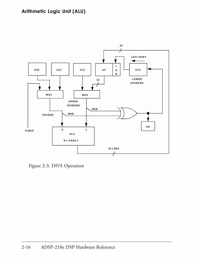
Arithmetic Logic Unit (ALU)
MUX
L
S
B
AX1 AY1 A FAX0 AY0
LOWER
DIVIDEND
R-BUS
LEFT SHIFT
15
MUX
UPPER
DIVIDEND
MSB
DIVISOR MSB
AQX Y
ALU
R = PASS Y
15 LSBS
16
Figure 2-3. DIVS Operation
2-16 ADSP-218x DSP Hardware Reference

Computational Units
When dividing unsigned numbers, the DIVS operation is not used. Instead, the AQ bit in the arithmetic status register (ASTAT) should be initialized to zero by manually clearing it. The AQ bit indicates to the following opera-tions that the quotient should be assumed positive.
The second division primitive is the “divide-quotient” (DIVQ) instruction which generates one bit of quotient at a time and is executed repeatedly to compute the remaining quotient bits. For unsigned single precision divides, the DIVQ instruction is executed 16 times to produce 16 quotient bits. For signed single precision divides, the DIVQ instruction is executed 15 times after the sign bit is computed by the DIVS operation.
DIVQ instruction shifts the AY0 register left by one bit so that the new quo-tient bit can be moved into the LSB position. The status of the AQ bit generated from the previous operation determines the ALU operation to calculate the partial remainder. If AQ = 1, the ALU adds the divisor to the partial remainder in AF. If AQ = 0, the ALU subtracts the divisor from the partial remainder in AF. The ALU output R is offset loaded into AF just as with the DIVS operation. The AQ bit is computed as the exclusive-OR of the divisor MSB and the ALU output MSB, and the quotient bit is this value inverted. The quotient bit is loaded into the LSB of the AY0 register which is also shifted left by one bit. The DIVQ operation is illustrated in Figure 2-4.
ADSP-218x DSP Hardware Reference 2-17

Arithmetic Logic Unit (ALU)
MUX
AX1AX0
R-BUS
DIVISOR MSB
AQX Y
ALU
1 MSB
L
S
BAF AY0
LOWER
DIVIDE ND
LEFT SHIFT
15
PARTIAL
REMAINDER
16
R=Y+X IF AQ=1
R=Y-X IF AQ=0
15 LSB S
Figure 2-4. DIVQ Operation
2-18 ADSP-218x DSP Hardware Reference

Computational Units
The format of the quotient for any numeric representation can be deter-mined by the format of the dividend and divisor. For example, let NL represent the number of bits to the left of the binary point and NR repre-sent the number of bits to the right of the binary point of the dividend. Let DL represent the number of bits to the left of the binary point and DR represent the number of bits to the right of the binary point of the divisor. Then, the quotient has NL–DL+1 bits to the left of the binary point and NR–DR–1 bits to the right of the binary point.
Some format manipulation may be necessary to guarantee the validity of the quotient. For example, if both operands are signed and fully fractional (dividend in 1.31 format and divisor in 1.15 format) the result is fully fractional (in 1.15 format) and therefore the dividend must be smaller than the divisor for a valid result.
To divide two integers (dividend in 32.0 format and divisor in 16.0 for-mat) and produce an integer quotient (in 16.0 format), you must shift the dividend one bit to the left (into 31.1 format) before dividing. Additional discussion and code examples can be found in the ADSP-218x Instruction Set Reference.
D IV ID E N D
N L B IT S N R B IT S
D IV IS O R B B . B B B B B B B B B B B B B B
D L B IT S D R B IT S
Q U O T IE N T B B B B .B B B B B B B B B B B B
(N L – D L + 1 ) B IT S (N R – D R – 1 ) B IT S
B B B B B . B B B B B B B B B B B B B B B B B B B B B B B B B B B
Figure 2-5. Quotient Format
ADSP-218x DSP Hardware Reference 2-19
Multiplier Accumulator (MAC)
The algorithm overflows if the result cannot be represented in the format of the quotient, as calculated above, or if the divisor is zero or less than the dividend in magnitude.
ALU StatusThe ALU status bits in the ASTAT register are defined below. Complete information about the ASTAT register and specific bit mnemonics and posi-tions is provided in the Program Control chapter.
Multiplier Accumulator (MAC)The multiplier/accumulator (MAC) provides high-speed multiplication, multiplication with cumulative addition, multiplication with cumulative subtraction, saturation and clear-to-zero functions. A feedback function allows part of the accumulator output to be directly used as one of the multiplicands on the next cycle.
Table 2-6. ALU Status Bits in the ASTAT Register
Flag Name Definition
AZ Zero Logical NOR of all the bits in the ALU result register. True if ALU out-put equals zero.
AN Negative Sign bit of the ALU result. True if the ALU output is negative.
AV Overflow Exclusive-OR of the carry outputs of the two most significant adder stages. True if the ALU overflows.
AC Carry Carry output from the most significant adder stage.
AS Sign Sign bit of the ALU X input port. Affected only by the ABS instruc-tion.
AQ Quotient Quotient bit generated only by the DIVS and DIVQ instructions.
2-20 ADSP-218x DSP Hardware Reference

Computational Units
MAC StructureFigure 2-6 shows a block diagram of the multiplier/accumulator.
NOTE: T he MR2 registe ris 8 bits aligned on thelower 8 bits of both the Rand DM D bus es
Figure 2-6. MAC Block Diagram
ADSP-218x DSP Hardware Reference 2-21

Multiplier Accumulator (MAC)
The multiplier has two 16-bit input ports, X and Y, and a 32-bit product output port, P. The 32-bit product is passed to a 40-bit adder/subtracter, which adds or subtracts the new product from the content of the multi-plier result (MR) register or passes the new product directly to MR. The MR register is 40 bits wide. In this manual, we refer to the entire register as MR. The register actually consists of three smaller registers: MR0 and MR1 which are 16 bits wide and MR2 which is 8 bits wide.
The adder/subtracter is greater than 32 bits to allow for intermediate over-flow in a series of multiply/accumulate operations. The multiply overflow (MV) status bit is set when the accumulator has overflowed beyond the 32-bit boundary; that is, when there are significant (non-sign) bits in the top nine bits of the MR register (based on twos-complement arithmetic).
The input/output registers of the MAC are similar to the ALU. The X input port can accept data from either the MX register file or from any reg-ister on the result (R) bus. The R bus connects the output registers of all the computational units, permitting them to be used as input operands directly. There are two registers in the MX register file, MX0 and MX1. These registers can be read and written from the DMD bus. The MX register file outputs are dual-ported so that one register can provide input to the mul-tiplier while either one simultaneously drives the DMD bus.
The Y input port can accept data from either the MY register file or the MF register. The MY register file has two registers, MY0 and MY1; these registers can be read and written from the DMD bus and written from the PMD bus. The instruction set also provides for reading these registers over the PMD bus, but there is no direct connection; this operation uses the PMD-DMD bus exchange unit. The MY register file outputs are also dual-ported so that one register can provide input to the multiplier while either one simultaneously drives the DMD bus.
2-22 ADSP-218x DSP Hardware Reference

Computational Units
The output of the adder/subtracter goes to either the MF register or the MR register. The MF register is a feedback register which allows bits 16–31 of the result to be used directly as the multiplier Y input on a subsequent cycle. The 40-bit adder/subtracter register (MR) is divided into three sec-tions: MR2, MR1, and MR0. Each of these registers can be loaded directly from the DMD bus and output to either the DMD bus or the R bus.
Any of the registers associated with the MAC can be both read and written in the same cycle. Registers are read at the beginning of the cycle and writ-ten at the end of the cycle. A register read, therefore, reads the value loaded at the end of a previous cycle. A new value written to a register can-not be read out until a subsequent cycle. This allows an input register to provide an operand to the MAC at the beginning of the cycle and be updated with the next operand from memory at the end of the same cycle. It also allows a result register to be stored in memory and updated with a new result in the same cycle. See “Multifunction Instructions” in the ADSP-218x DSP Instruction Set Reference for an illustration of this same-cycle read and write.
The MAC contains a duplicate bank of registers, shown in Figure 2-6 behind the primary registers. There are actually two sets of MR, MF, MX, and MY register files. Only one bank is accessible at a time. The additional bank of registers can be activated for extremely fast context switching. A new task, such as an interrupt service routine, can be executed without trans-ferring current states to storage.
The selection of the primary or alternate bank of registers is controlled by the ena sec_reg and dis sec_reg assembly instructions or by bit zero in the MSTAT register. The alternate bank of registers is activated by the ena sec_reg instruction or by setting bit zero of MSTAT to a 1. The primary bank of registers is activated by executing the dis sec_reg instruction or by clearing bit zero of MSTAT. Upon reset, the primary bank of registers is active by default.
ADSP-218x DSP Hardware Reference 2-23

Multiplier Accumulator (MAC)
The ADSP-218x processors also offer an xop * xop squaring operation. Both xops must be in the same register. This option allows single-cycle X2 and ∑X2 instructions.
The data format selection field following the two operands specifies whether each respective operand is in Signed (S) or Unsigned (U) format. The data format selection field must be (UU), (SS), or (RND) only. There is no default; one of the data formats must be specified.
If RND (Round) is specified, the MAC multiplies the two source oper-ands, rounds the result to the most significant 24 bits (or rounds bits 31-16 to 16 bits if there is no overflow from the multiply), and stores the result in the destination register. The two multiplication operands xop and xop are considered to be in twos complement format. Rounding can be biased or unbiased. For more information, see “Rounding Mode” on page 2-30.
MAC OperationsThis section explains the functions of the MAC, its input formats and its handling of overflow and saturation.
Standard Functions
Table 2-7 lists the functions performed by the MAC.
Table 2-7. Standard MAC Functions
Function Description
MR = xop * yop Multiply X and Y operands.
MR = xop * xop Multiply X and X operands.
MR = MR + xop * yop Multiply X and Y operands and add result to MR.
2-24 ADSP-218x DSP Hardware Reference

Computational Units
The ADSP-218x family provides two modes for the standard multi-ply/accumulate function: fractional mode for fractional numbers (1.15), and integer mode for integers (16.0).
Fractional mode is selected by default upon reset or by the DIS M_MODE instruction. Integer mode is selected by the ENA M_MODE instruction. These instructions set or clear bit 4 of MSTAT. This bit is set to 0 for fractional mode and 1 for integer mode. In either mode, the multiplier output P is fed into a 40-bit adder/subtracter, which adds or subtracts the new prod-uct with the current contents of the MR register to form the final 40-bit result R.
In the fractional mode, the 32-bit P output is format adjusted, that is, sign-extended and shifted one bit to the left before being added to MR. For example, bit 31 of P lines up with bit 32 of MR (which is bit 0 of MR2) and bit 0 of P lines up with bit 1 of MR (which is bit 1 of MR0). The LSB is zero-filled. The fractional multiplier result format is shown in Figure 2-7.
MR = MR – xop * yop Multiply X and Y operands and subtract result from MR.
MR = 0 Clear result (MR) to zero.
Table 2-7. Standard MAC Functions
Function Description
ADSP-218x DSP Hardware Reference 2-25

Multiplier Accumulator (MAC)
In the integer mode, the 32-bit P register is not shifted before being added to MR. Figure 2-8 shows the integer-mode result placement.
31 31 31 31 31 31 31 31 30 29 28 27 26 25 24 23 22 21 20 19 18 17 16 15 14 13 12 11 10 9 8 7 6 5 4 3 2 1 0
15 14 13 12 11 10 9 8 7 6 5 4 3 2 1 015 14 13 12 11 10 9 8 7 6 5 4 3 2 1 07 6 5 4 3 2 1 0
MR2 MR1 MR0
P SIGN M U LTIPLIER P OUTPU T
Figure 2-7. Fractional Multiplier Result Format
31
15 14 13 12 11 10 9 8 7 6 5 4 3 2 1 015 14 13 12 11 10 9 8 7 6 5 4 3 2 1 07 6 5 4 3 2 1 0
MR2 MR1 MR0
31 31 31 31 31 31 31 31 30 29 28 27 26 25 24 23 22 21 20 19 18 17 16 15 14 13 12 11 10 9 8 7 6 5 4 3 2 1 0
P SIGN MULTIPLIER P OUTPUT
Figure 2-8. Integer Multiplier Results Format
2-26 ADSP-218x DSP Hardware Reference

Computational Units
Input Formats
To facilitate multiprecision multiplications, the multiplier accepts X and Y inputs represented in any combination of signed twos-complement for-mat and unsigned format, as shown in Table 2-8:
The input formats are specified as part of the instruction. These are dynamically selectable each time the multiplier is used.
The (signed x signed) mode is used when multiplying two signed single precision numbers or the two upper portions of two signed multiprecision numbers.
The (unsigned x signed) and (signed x unsigned) modes are used when multiplying the upper portion of a signed multiprecision number with the lower portion of another or when multiplying a signed single precision number by an unsigned single precision number.
The (unsigned x unsigned) mode is used when multiplying unsigned sin-gle precision numbers or the non-upper portions of two signed multiprecision numbers.
Table 2-8. X and Y Inputs
X Input Y Input Code Example
Signed x Signed MR=MX0*MY0(SS)
Unsigned x Signed MR=MX0*MY0(US)
Signed x Unsigned MR=MX0*MY0(SU)
Unsigned x Unsigned MR=MX0*MY0(UU)
ADSP-218x DSP Hardware Reference 2-27
Multiplier Accumulator (MAC)
MAC Input/Output Registers
Table 2-9 lists the sources for MAC input and output registers.
MR Register Operation
As described, and shown on the block diagram, the MR register is divided into three sections: MR0 (bits 0-15), MR1 (bits 16-31), and MR2 (bits 32-39). Each of these registers can be loaded from the DMD bus and output to the R bus or the DMD bus.
The 8-bit MR2 register is tied to the lower 8 bits of these buses. When MR2 is output onto the DMD bus or the R bus, it is sign extended to form a 16-bit value. MR1 also has an automatic sign-extend capability. When MR1 is loaded from the DMD bus, every bit in MR2 will be set to the sign bit (MSB) of MR1, so that MR2 appears as an extension of MR1. To load the MR2 register with a value other than MR1’s sign extension, you must load MR2 after MR1 has been loaded. Loading MR0 affects neither MR1 nor MR2; no sign extension occurs in MR0 loads.
Table 2-9. Sources for MAC Input and Output Registers
Source for X Input Port Source for Y Input Port Destination for R Output Port
MX0, MX1 MY0, MY1 MR (MR2, MR1, MR0)
AR MF MF
MR0, MR1, MR2
SR0, SR1
2-28 ADSP-218x DSP Hardware Reference

Computational Units
MAC Overflow And Saturation
The adder/subtracter generates an overflow status signal (MV), which is loaded into the processor arithmetic status (ASTAT) every time a MAC operation is executed. The MV bit is set when the accumulator result, inter-preted as a twos-complement number, crosses the 32-bit (MR1/MR2) boundary. That is, MV is set if the upper nine bits of MR are not all ones or all zeros.
The MR register has a saturation capability that sets MR to the maximum positive or negative value if an overflow or underflow has occurred. The saturation operation depends on the overflow status bit (MV) in the proces-sor arithmetic status (ASTAT) and the MSB of the MR2 register.
! The MF register cannot be saturated.
The MV flag is set/cleared after MAC operations only. When the MR0, MR1, or MR2 registers are loaded by Move instructions, the instruc-tion MR = MR can be used to update the MV flag.
Table 2-10 summarizes the MR saturation operation.
Saturation in the MAC is an instruction rather than a mode as in the ALU. The saturation instruction is intended to be used at the completion of a string of multiplication/accumulations so that intermediate overflows do not cause the accumulator to saturate.
Table 2-10. Effect of MAC Saturation Instruction
MV MSB of MR2
MR contents after saturation
0 0 or 1 no change
1 0 00000000 0111111111111111 1111111111111111 full-scale positive
1 1 11111111 1000000000000000 0000000000000000 full-scale negative
ADSP-218x DSP Hardware Reference 2-29

Multiplier Accumulator (MAC)
Overflowing beyond the MSB of MR2 should never be allowed. The true sign bit of the result is then irretrievably lost and saturation may not pro-duce a correct value. It takes more than 255 overflows (MV type) to reach this state, however.
Rounding Mode
The accumulator has the capability for rounding the 40-bit result R at the boundary between bit 15 and bit 16. Rounding can be specified as part of the instruction code. The rounded output is directed to either MR or MF. When rounding is invoked with MF as the output register, register contents in MF represent the rounded 16-bit result. Similarly, when MR is selected as the output, MR1 contains the rounded 16-bit result; the rounding effect in MR1 affects MR2 as well and MR2 and MR1 represent the rounded 24-bit result.
The accumulator uses an unbiased rounding scheme. The conventional method of biased rounding is to add a 1 into bit position 15 of the adder chain. This method causes a net positive bias since the midway value (when MR0=0x8000) is always rounded upward. The accumulator elimi-nates this bias by forcing bit 16 in the result output to zero when it detects this midway point. This has the effect of rounding odd MR1 values upward and even MR1 values downward, yielding a zero large-sample bias assuming uniformly distributed values.
Using x to represent any bit pattern (not all zeros), here are two examples of rounding. The example in Figure 2-9 shows a typical rounding opera-tion for MR; these also apply for SR.
...MR2..|.......MR1......|.......MR0......xxxxxxxx|xxxxxxxx00100101|1xxxxxxxxxxxxxxx........|................|1...............xxxxxxxx|xxxxxxxx00100110|0xxxxxxxxxxxxxxx
Unrounded value:Add 1 and carry:Rounded value:
Figure 2-9. Typical Unbiased Multiplier Rounding Operation
2-30 ADSP-218x DSP Hardware Reference

Computational Units
The compensation to avoid net bias becomes visible when the lower 15 bits are all zero and bit 15 is one (the midpoint value) as shown in Figure 2-10.
Biased Rounding
The BIASRND bit in the SPORT0 autobuffer control register enables biased rounding. When the BIASRND bit is cleared (=0), the RND option in mul-tiplier instructions uses the normal unbiased rounding operation (as discussed in “Rounding Mode” on page 2-30). When the BIASRND bit is set to 1, the DSP uses biased rounding instead of unbiased rounding. When operating in biased rounding mode, all rounding operations with MR0 set to 0x8000 round up, rather than only rounding odd MR1 values up. For an example, see Figure 2-11.
This mode only has an effect when the MR0 register contains 0x8000; all other rounding operations work normally. This mode allows more effi-cient implementation of bit-specified algorithms that use biased rounding, for example the GSM speech compression routines. Unbiased rounding is preferred for most algorithms.
...MR2..|.......MR1......|.......MR0......xxxxxxxx|xxxxxxxx01100110|1000000000000000........|................|1...............xxxxxxxx|xxxxxxxx01100111|0000000000000000
Unrounded value:Add 1 and carry:MR bit 16=1:
xxxxxxxx|xxxxxxxx01100110|0000000000000000Rounded value:
Figure 2-10. Avoiding Net Bias in Unbiased Multiplier Rounding Operation
ADSP-218x DSP Hardware Reference 2-31

Barrel Shifter
Barrel ShifterThe barrel shifter (shifter) provides a complete set of shifting functions for 16-bit inputs, yielding a 32-bit output. These include arithmetic shift, logical shift and normalization. The shifter also performs derivation of exponent and derivation of common exponent for an entire block of num-bers. These basic functions can be combined to efficiently implement any degree of numerical format control, including full floating-point representation.
Shifter StructureFigure 2-12 shows a block diagram of the shifter. The shifter can be divided into the following components: the shifter array, the OR/PASS logic, the exponent detector, and the exponent compare logic.
0x00 0000 8000 0x00 0001 0000 0x00 0000 00000x00 0001 8000 0x00 0002 0000 0x00 0002 00000x00 0000 8001 0x00 0001 0001 0x00 0001 00010x00 0001 8001 0x00 0002 0001 0x00 0002 00010x00 0000 7FFF 0x00 0000 FFFF 0x00 0000 FFFF0x00 0001 7FFF 0x00 0001 FFFF 0x00 0001 FFFF
MR before RND
Biased RND result
Unbiased RND result
Figure 2-11. Bias Rounding in Multiplier Operation
2-32 ADSP-218x DSP Hardware Reference

Computational Units
The shifter array is a 16x32 barrel shifter. It accepts a 16-bit input and can place it anywhere in the 32-bit output field, from off-scale right to off-scale left, in a single cycle. This gives 49 possible placements within the 32-bit field. The placement of the 16 input bits is determined by a control code (C) and a HI/LO reference signal.
The shifter array and its associated logic are surrounded by a set of regis-ters. The shifter input (SI) register provides input to the shifter array and the exponent detector. The SI register is 16 bits wide and is readable and writable from the DMD bus. The shifter array and the exponent detector also take as inputs AR, SR or MR via the R bus. The shifter result (SR) regis-ter is 32 bits wide and is divided into two 16-bit sections, SR0 and SR1. The SR0 and SR1 registers can be loaded from the DMD bus and output to either the DMD bus or the R bus. The SR register is also fed back to the OR/PASS logic to allow double-precision shift operations.
The SE register (“shifter exponent”) is 8 bits wide and holds the exponent during the normalize and denormalize operations. The SE register is load-able and readable from the lower 8 bits of the DMD bus. It is a twos-complement, 8.0 value.
The SB register (“shifter block”) is important in block floating-point oper-ations where it holds the block exponent value, that is, the value by which the block values must be shifted to normalize the largest value. The SB reg-ister is 5 bits wide and holds the most recent block exponent value. The SB register is loadable and readable from the lower 5 bits of the DMD bus. It is a twos-complement, 5.0 value.
Whenever the SE or SB registers are output onto the DMD bus, they are sign-extended to form a 16-bit value.
ADSP-218x DSP Hardware Reference 2-33

Barrel Shifter
MUX
16
32
SR1REGISTER
SR0REGISTER
16
SIREGISTER
SBREGISTER
MUX
MUX
SEREGISTER
NEGATE
MUX
COMPAREEXPONENTDETECTOR
HI / LO SHIFTERARRAY
I
RC
X
O
OR / PASS
MUXMUX
8
32
16
1616
From INSTRUCTION
16
8
MUX
SS
DMD BUS
R - BUS
X
Figure 2-12. Shifter Block Diagram
2-34 ADSP-218x DSP Hardware Reference

Computational Units
Any of the SI, SE or SR registers can be read and written in the same cycle. Registers are read at the beginning of the cycle and written at the end of the cycle. All register reads, therefore, read values loaded at the end of a previous cycle. A new value written to a register cannot be read out until a subsequent cycle. This allows an input register to provide an operand to the shifter at the beginning of the cycle and be updated with the next operand at the end of the same cycle. It also allows a result register to be stored in memory and updated with a new result in the same cycle. See “Multifunction Instructions” in the ADSP-218x DSP Instruction Set Refer-ence for an illustration of this same-cycle read and write.
The shifter contains a duplicate bank of registers behind the primary regis-ters (see Figure 2-12). There are actually two sets of SE, SB, SI, SR1, and SR0 registers. Only one bank is accessible at a time. The additional bank of registers can be activated for extremely fast context switching. A new task, such as an interrupt service routine, can then be executed without trans-ferring current states to storage.
The selection of the primary or alternate bank of registers is controlled by the ena sec_reg and dis sec_reg assembly instructions or by bit zero in the MSTAT register. The alternate bank of registers is activated by the ena sec_reg instruction or by setting bit zero of MSTAT to a 1. The primary bank of registers is activated by executing the dis sec_reg instruction or by clearing bit zero of MSTAT. Upon reset, the primary bank of registers is active by default.
The shifting of the input is determined by a control code (C) and a HI/LO reference signal. The control code is an 8-bit signed value which indicates the direction and number of places the input is to be shifted. Positive codes indicate a left shift (upshift) and negative codes indicate a right shift (downshift). The control code can come from three sources: the content of the shifter exponent (SE) register, the negated content of the SE register or an immediate value from the instruction.
ADSP-218x DSP Hardware Reference 2-35

Barrel Shifter
The HI/LO signal determines the reference point for the shifting. In the HI state, all shifts are referenced to SR1 (the upper half of the output field), and in the LO state, all shifts are referenced to SR0 (the lower half). The HI/LO reference feature is useful when shifting 32-bit values since it allows both halves of the number to be shifted with the same control code. The HI/LO reference signal is selectable each time the shifter is used.
The shifter fills any bits to the right of the input value in the output field with zeros, and bits to the left are filled with the extension bit (X). The extension bit can be fed by three possible sources depending on the instruction being performed. The three sources are the MSB of the input, the AC bit from the arithmetic status register (ASTAT) or a zero.
Figure 2-13 on page 2-37 shows the shifter array output as a function of the control code and HI/LO signal.
The OR/PASS logic allows the shifted sections of a multiprecision num-ber to be combined into a single quantity. In some shifter instructions, the shifted output may be logically ORed with the contents of the SR register; the shifter array is bitwise ORed with the current contents of the SR regis-ter before being loaded there. When the [SR OR] option is not used in the instruction, the shifter array output is passed through and loaded into the shifter result (SR) register unmodified.
The exponent detector derives an exponent for the shifter input value. The exponent detector operates in one of three ways, which determine how the input value is interpreted. In the HI state, the input is interpreted as a single precision number or the upper half of a double precision num-ber. The exponent detector determines the number of leading sign bits and produces a code that indicates how many places the input must be up-shifted to eliminate all but one of the sign bits. The code is negative so that it can become the effective exponent for the mantissa formed by removing the redundant sign bits.
2-36 ADSP-218x DSP Hardware Reference

Computational Units
Control Code Shifter Array Output HI Reference
+16 to +127 +32 to +127 00000000 00000000 00000000 00000000+15 +31 R0000000 00000000 00000000 00000000+14 +30 PR000000 00000000 00000000 00000000+13 +29 NPR00000 00000000 00000000 00000000+12 +28 MNPR0000 00000000 00000000 00000000+11 +27 LMNPR000 00000000 00000000 00000000+10 +26 KLMNPR00 00000000 00000000 00000000+9 +25 JKLMNPR0 00000000 00000000 00000000+8 +24 IJKLMNPR 00000000 00000000 00000000+7 +23 HIJKLMNP R0000000 00000000 00000000+6 +22 GHIJKLMN PR000000 00000000 00000000+5 +21 FGHIJKLM NPR00000 00000000 00000000+4 +20 EFGHIJKL MNPR0000 00000000 00000000+3 +19 DEFGHIJK LMNPR000 00000000 00000000+2 +18 CDEFGHIJ KLMNPR00 00000000 00000000+1 +17 BCDEFGHI JKLMNPR0 00000000 000000000 +16 ABCDEFGH IJKLMNPR 00000000 00000000
-1 +15 XABCDEFG HIJKLMNP R0000000 00000000-2 +14 XXABCDEF GHIJKLMN PR000000 00000000-3 +13 XXXABCDE FGHIJKLM NPR00000 00000000-4 +12 XXXXABCD EFGHIJKL MNPR0000 00000000-5 +11 XXXXXABC DEFGHIJK LMNPR000 00000000-6 +10 XXXXXXAB CDEFGHIJ KLMNPR00 00000000-7 +9 XXXXXXXA BCDEFGHI JKLMNPR0 00000000-8 +8 XXXXXXXX ABCDEFGH IJKLMNPR 00000000-9 +7 XXXXXXXX XABCDEFG HIJKLMNP R0000000-10 +6 XXXXXXXX XXABCDEF GHIJKLMN PR000000-11 +5 XXXXXXXX XXXABCDE FGHIJKLM NPR00000-12 +4 XXXXXXXX XXXXABCD EFGHIJKL MNPR0000-13 +3 XXXXXXXX XXXXXABC DEFGHIJK LMNPR000-14 +2 XXXXXXXX XXXXXXAB CDEFGHIJ KLMNPR00-15 +1 XXXXXXXX XXXXXXXA BCDEFGHI JKLMNPR0-16 0 XXXXXXXX XXXXXXXX ABCDEFGH IJKLMNPR-17 -1 XXXXXXXX XXXXXXXX XABCDEFG HIJKLMNP-18 -2 XXXXXXXX XXXXXXXX XXABCDEF GHIJKLMN-19 -3 XXXXXXXX XXXXXXXX XXXABCDE FGHIJKLM-20 -4 XXXXXXXX XXXXXXXX XXXXABCD EFGHIJKL-21 -5 XXXXXXXX XXXXXXXX XXXXXABC DEFGHIJK-22 -6 XXXXXXXX XXXXXXXX XXXXXXAB CDEFGHIJ-23 -7 XXXXXXXX XXXXXXXX XXXXXXXA BCDEFGHI-24 -8 XXXXXXXX XXXXXXXX XXXXXXXX ABCDEFGH-25 -9 XXXXXXXX XXXXXXXX XXXXXXXX XABCDEFG-26 -10 XXXXXXXX XXXXXXXX XXXXXXXX XXABCDEF-27 -11 XXXXXXXX XXXXXXXX XXXXXXXX XXXABCDE-28 -12 XXXXXXXX XXXXXXXX XXXXXXXX XXXXABCD-29 -13 XXXXXXXX XXXXXXXX XXXXXXXX XXXXXABC-30 -14 XXXXXXXX XXXXXXXX XXXXXXXX XXXXXXAB-31 -15 XXXXXXXX XXXXXXXX XXXXXXXX XXXXXXXA-32 to -128 -16 to -128 XXXXXXXX XXXXXXXX XXXXXXXX XXXXXXXX
LEGEND:ABCDEFGHIJKLMNPR representsthe 16-bit input pattern
X stands for the extension bit LO Reference
Figure 2-13. Shifter Array Output
ADSP-218x DSP Hardware Reference 2-37

Barrel Shifter
In the HI-extend state (HIX), the input is interpreted as the result of an add or subtract performed in the ALU which may have overflowed. Therefore the exponent detector takes the arithmetic overflow (AV) status into con-sideration. If AV is set, then a +1 exponent is output to indicate an extra bit is needed in the normalized mantissa (the ALU Carry bit); if AV is not set, then HI-extend functions exactly like the HI state. When performing a derive exponent function in HI or HI-extend modes, the exponent detector also outputs a shifter sign (SS) bit which is loaded into the arithmetic sta-tus register (ASTAT). The sign bit is the same as the MSB of the shifter input except when AV is set; when AV is set in HI-extend state, the MSB is inverted to restore the sign bit of the overflowed value.
In the LO state, the input is interpreted as the lower half of a double preci-sion number. In the LO state, the exponent detector interprets the SS bit in the arithmetic status register (ASTAT) as the sign bit of the number. The SE register is loaded with the output of the exponent detector only if SE con-tains –15. This occurs only when the upper half–which must be processed first–contained all sign bits. The exponent detector output is also offset by –16 to account for the fact that the input is actually the lower half of a 32-bit value. Figure 2-14 gives the exponent detector characteristics for all three modes.
The exponent compare logic is used to find the largest exponent value in an array of shifter input values. The exponent compare logic in conjunc-tion with the exponent detector derives a block exponent. The comparator compares the exponent value derived by the exponent detector with the value stored in the shifter block exponent (SB) register and updates the SB register only when the derived exponent value is larger than the value in SB register. See the examples shown in the following sections.
2-38 ADSP-218x DSP Hardware Reference

Computational Units
S = Sign bit
N = Non-sign bit
LEGEND
HI Mode HIX Mode
Shifter Array Input Output AV Output
1 DDDDDDDD DDDDDDDD +1SNDDDDDD DDDDDDDD 0 0 SNDDDDDD DDDDDDDD 0SSNDDDDD DDDDDDDD -1 0 SSNDDDDD DDDDDDDD -1SSSNDDDD DDDDDDDD -2 0 SSSNDDDD DDDDDDDD -2SSSSNDDD DDDDDDDD -3 0 SSSSNDDD DDDDDDDD -3SSSSSNDD DDDDDDDD -4 0 SSSSSNDD DDDDDDDD -4SSSSSSND DDDDDDDD -5 0 SSSSSSND DDDDDDDD -5SSSSSSSN DDDDDDDD -6 0 SSSSSSSN DDDDDDDD -6SSSSSSSS NDDDDDDD -7 0 SSSSSSSS NDDDDDDD -7SSSSSSSS SNDDDDDD -8 0 SSSSSSSS SNDDDDDD -8SSSSSSSS SSNDDDDD -9 0 SSSSSSSS SSNDDDDD -9SSSSSSSS SSSNDDDD -10 0 SSSSSSSS SSSNDDDD -10SSSSSSSS SSSSNDDD -11 0 SSSSSSSS SSSSNDDD -11SSSSSSSS SSSSSNDD -12 0 SSSSSSSS SSSSSNDD -12SSSSSSSS SSSSSSND -13 0 SSSSSSSS SSSSSSND -13SSSSSSSS SSSSSSSN -14 0 SSSSSSSS SSSSSSSN -14SSSSSSSS SSSSSSSS -15 0 SSSSSSSS SSSSSSSS -15
LO Mode
SS Output
S NDDDDDDD DDDDDDDD -15S SNDDDDDD DDDDDDDD -16S SSNDDDDD DDDDDDDD -17S SSSNDDDD DDDDDDDD -18S SSSSNDDD DDDDDDDD -19S SSSSSNDD DDDDDDDD -20S SSSSSSND DDDDDDDD -21S SSSSSSSN DDDDDDDD -22S SSSSSSSS NDDDDDDD -23S SSSSSSSS SNDDDDDD -24S SSSSSSSS SSNDDDDD -25S SSSSSSSS SSSNDDDD -26S SSSSSSSS SSSSNDDD -27S SSSSSSSS SSSSSNDD -28S SSSSSSSS SSSSSSND -29S SSSSSSSS SSSSSSSN -30S SSSSSSSS SSSSSSSS -31
Shifter Array Input
Shifter Array Input
D = Don't care bit
Figure 2-14. Exponent Detector Characteristics
ADSP-218x DSP Hardware Reference 2-39

Barrel Shifter
Shifter OperationsThe shifter performs the following functions (instruction mnemonics shown in parentheses):
• Arithmetic Shift (ASHIFT)
• Logical Shift (LSHIFT)
• Normalize (NORM)
• Derive Exponent (EXP)
• Block Exponent Adjust (EXPADJ)
These basic shifter instructions can be used in a variety of ways, depending on the underlying arithmetic requirements. The following sections present single and multiple precision examples for these functions:
• Derivation of a Block Exponent
• Immediate Shifts
• Denormalization
• Normalization
The shift functions (arithmetic shift, logical shift, and normalize) can be optionally specified with [SR OR] and HI/LO modes to facilitate multipreci-sion operations. [SR OR] logically ORs the shift result with the current contents of SR. This option is used to join two 16-bit quantities into a 32-bit value in SR. When [SR OR] is not used, the shift value is passed through to SR directly. The HI and LO modifiers reference the shift to the upper or lower half of the 32-bit SR register. These shift functions take inputs from either the SI register or any other result register and load the 32-bit shifted result into the SR register.
2-40 ADSP-218x DSP Hardware Reference

Computational Units
Shifter Input/Output Registers
Table 2-11 shows the sources of shifter input and output.
Derive Block Exponent
The EXPADJ instruction detects the exponent of the number largest in magnitude in an array of numbers. The steps for a typical block exponent derivation are as follows:
1. Load SB with –16. The SB register contains the exponent for the entire block. The possible values at the conclusion of a series of EXPADJ operations range from –15 to 0. The exponent compare logic updates the SB register if the new value is greater than the cur-rent value. Loading the register with –16 initializes it to a value certain to be less than any actual exponents detected.
2. Process the first array element, as follows:
Array(1) = 11110101 10110001Exponent = –3
–3 > SB (–16)SB gets –3
Table 2-11. Shifter Input and Output
Source for Shifter Input Destination for Shifter Output
SI SR (SR0, SR1)
AR
MR0, MR1, MR2
SR0, SR1
ADSP-218x DSP Hardware Reference 2-41

Barrel Shifter
3. Process next array element, as follows:
Array(2)= 00000001 01110110Exponent = –6
–6 < –3SB remains –3
4. Continue processing array elements.
When and if an array element is found whose exponent is greater than SB, that value is loaded into SB. When all array elements have been processed, the SB register contains the exponent of the largest number in the entire block. No normalization is performed. EXPADJ is purely an inspection operation. The value in SB could be transferred to SE and used to normal-ize the block on the next pass through the shifter. Or, SB could be associated with that data for subsequent interpretation.
Immediate Shifts
An immediate shift simply shifts the input bit pattern to the right (down-shift) or left (upshift) by a given number of bits. Immediate shift instructions use the data value in the instruction itself to control the amount and direction of the shifting operation. (See the ADSP-218x DSP Instruction Set Reference for examples of this instruction.) The data value controlling the shift is an 8-bit signed number. The SE register is not used or changed by an immediate shift.
The following example shows the input value downshifted relative to the upper half of SR (SR1). This is the (HI) version of the shift:
SI=0xB6A3;SR=LSHIFT SI BY –5 (HI);
Input: 10110110 10100011
Shift value: –5
SR: 00000101 10110101 00011000 000000
2-42 ADSP-218x DSP Hardware Reference
Computational Units
Here is the same input value shifted in the other direction, referenced to the lower half (LO) of SR:
SI=0xB6A3;SR=LSHIFT SI BY 5 (LO);
Input: 10110110 10100011
Shift value: +5
SR: 00000000 00010110 11010100 01100000
In addition to the direction of the shifting operation, the shift may be either arithmetic (ASHIFT) or logical (LSHIFT). For example, the following shows a logical shift, relative to the upper half of SR (HI):
SI=0xB6A3;SR=LSHIFT SI BY –5 (HI);
Input: 10110110 10100011Shift value: -5
SR: 00000101 10110101 00011000 00000000
This example shows an arithmetic shift of the same input and shift code:
SI=0xB6A3;SR=ASHIFT SI BY –5 (HI);
Input: 10110110 10100011
Shift value: -5
SR: 11111101 10110101 00011000 00000000
ADSP-218x DSP Hardware Reference 2-43

Barrel Shifter
Denormalize
Denormalizing refers to shifting a number according to a predefined expo-nent. The operation is effectively a floating-point to fixed-point conversion.
Denormalizing requires a sequence of operations. First, the SE register must contain the exponent value. This value may be explicitly loaded or may be the result of some previous operation. Next the shift itself is per-formed, taking its shift value from the SE register, not from an immediate data value.
Two examples of denormalizing a double-precision number are given below. The first shows a denormalization in which the upper half of the number is shifted first, followed by the lower half. Since computations may produce output in either order, the second example shows the same operation in the other order, i.e. lower half first.
Always select the arithmetic shift for the higher half (HI) of the twos-com-plement input (or logical for unsigned). Likewise, the first half processed does not use the [SR OR] option.
Modifier = HI, No [SR OR], Shift operation = Arithmetic, SE = –3
First Input: 10110110 10100011 (upper half of desired result)
SR: 11110110 11010100 01100000 00000000
Now the lower half is processed. Always select a logical shift for the lower half of the input. Likewise, the second half processed must use the [SR OR] option to avoid overwriting the previous half of the output value.
Modifier = LO, [SR OR], Shift operation = Logical, SE = –3
Second Input: 01110110 01011101 (lower half of desired result)
SR: 11110110 11010100 01101110 11001011
2-44 ADSP-218x DSP Hardware Reference

Computational Units
Here is the same input processed in the reverse order. The higher half is always arithmetically shifted and the lower half is logically shifted. The first input is passed straight through to SR, but the second half is ORed to create a double-precision value in SR.
Modifier = LO, No [SR OR], Shift operation = Logical, SE = –3
First Input: 01110110 01011101 (lower half of desired result)
SR: 00000000 00000000 00001110 11001011
Modifier = HI, [SR OR], Shift operation = Arithmetic, SE = –3
Second Input: 10110110 10100011 (upper half of desired result)
SR: 11110110 11010100 01101110 11001011
Normalize
Numbers with redundant sign bits require normalizing. Normalizing a number is the process of shifting a twos-complement number within a field so that the rightmost sign bit lines up with the MSB position of the field and recording how many places the number was shifted. The opera-tion can be thought of as a fixed-point to floating-point conversion, generating an exponent and a mantissa.
Normalizing is a two-stage process. The first stage derives the exponent. The second stage does the actual shifting. The first stage uses the EXP instruction which detects the exponent value and loads it into the SE regis-ter. This instruction (EXP) recognizes a (HI) and (LO) modifier. The second stage uses the NORM instruction. The NORM instruction recognizes (HI) and (LO) and also has the [SR OR] option. The NORM instruction uses the negated value of the SE register as its shift control code. The negated value is used so that the shift is made in the correct direction.
ADSP-218x DSP Hardware Reference 2-45

Barrel Shifter
Here is a normalization example for a single precision input:
SE=EXP AR (HI);
Detects Exponent With Modifier = HI
Input: 11110110 11010100
SE set to: –3
Normalize, with modifier = HI Shift driven by value in SE
Input: 11110110 11010100
SR: 10110110 10100000 00000000 00000000
For a single precision input, the normalize operation can use either the (HI) or (LO) modifier, depending on whether you want the result in SR1 or SR0, respectively.
Double precision values follow the same general scheme. The first stage detects the exponent and the second stage normalizes the two halves of the input. For double precision, however, there are two operations in each stage.
For the first stage, the upper half of the input must be operated on first. This first exponent derivation loads the exponent value into SE. The sec-ond exponent derivation, operating on the lower half of the number will not alter the SE register unless SE = –15. This happens only when the first half contained all sign bits. In this case, the second operation will load a value into SE. (See Figure 2-14 on page 2-39) This value is used to control both parts of the normalization that follows.
For the second stage, now that SE contains the correct exponent value, the order of operations is immaterial. The first half (whether HI or LO) is nor-malized without the [SR OR] and the second half is normalized with [SR OR] to create one double-precision value in SR. The (HI) and (LO) modifiers identify which half is being processed.
2-46 ADSP-218x DSP Hardware Reference

Computational Units
Here is a complete example of a typical double precision normalization.
1. Detect Exponent, Modifier = HI
First Input: 11110110 11010100 (Must be upper half)
SE set to: -3
2. Detect Exponent, Modifier = LO
Second Input: 01101110 11001011
SE unchanged, still -3
3. Normalize, Modifier = HI, No [SR OR], SE = –3
First Input: 11110110 11010100
SR: 10110110 10100000 00000000 00000000
4. Normalize, Modifier = LO, [SR OR], SE = –3
Second Input: 01101110 11001011
SR: 10110110 10100011 01110110 01011000
If the upper half of the input contains all sign bits, the SE register value is determined by the second derive exponent operation as shown in the fol-lowing example.
1. Detect Exponent, Modifier = HI
First Input: 11111111 11111111 (Must be upper half)
SE set to: -15
2. Detect Exponent, Modifier = LO
Second Input: 11110110 11010100
SE now set to: -19
ADSP-218x DSP Hardware Reference 2-47

Barrel Shifter
3. Normalize, Modifier = HI, No [SR OR], SE = –19 (negated)
First Input: 11111111 11111111
SR: 00000000 00000000 00000000 00000000
All values of SE less than –15 (resulting in a shift of +16 or more) upshift the input completely off scale.
4. Normalize, Modifier = LO, [SR OR], SE = –19 (negated)
Second Input: 11110110 11010100
SR: 10110110 10100000 00000000 00000000
There is one additional normalization situation, requiring the HI-extended (HIX) state. This is specifically when normalizing ALU results (AR) that may have overflowed. This operation reads the arithmetic status word (ASTAT) overflow bit (AV) and the carry bit (AC) in conjunction with the value in AR. AV is set (1) if an overflow has occurred. AC contains the true sign of the twos-complement value.
For example, given these conditions:
AR = 11111010 00110010
AV = 1, indicating overflowAC = 0, the true sign bit of this value
1. Detect Exponent, Modifier = HIX
SE gets set to +1
2. Normalize, Modifier = HI, SE = 1
AR = 11111010 00110010
SR = 01111101 00011001
The AC bit is supplied as the sign bit, shown in bold above.
2-48 ADSP-218x DSP Hardware Reference

Computational Units
The HIX operation executes properly whether or not there has actually been an overflow. Consider this example:
AR = 11100011 01011011
AV = 0, indicating no overflowAC = 0, not meaningful if AV = 0
1. Detect Exponent, Modifier = HIX
SE set to –2
2. Normalize, Modifier = HI, SE = –2
AR = 11100011 01011011
SR = 10001101 01101000 00000000 00000000
The AC bit is not used as the sign bit.
A brief examination of Figure 2-13 on page 2-37 shows that the HIX mode is identical to the HI mode when AV is not set. When the NORM, LO opera-tion is done, the extension bit is zero; when the NORM, HI operation is done, the extension bit is AC.
ADSP-218x DSP Hardware Reference 2-49

Barrel Shifter
2-50 ADSP-218x DSP Hardware Reference

3 PROGRAM SEQUENCERFigure 3-0.
Table 3-0.
Listing 3-0.
OverviewThis chapter describes the program sequencer of the ADSP-218x family processors. The program sequencer circuitry controls the flow of program execution. It contains an interrupt controller and status and condition logic.
The program sequencer generates a stream of instruction addresses and provides flexible control of program flow. It allows sequential instruction execution, zero-overhead looping, sophisticated interrupt servicing, and single-cycle branching with jumps and calls (both conditional and unconditional).
This chapter discusses each function on the program sequencer. It also dis-cusses both the program sequencer logic and the following instructions used to control program flow:
• DO UNTIL
• JUMP
• CALL
• RTS (Return from Subroutine)
• RTI (Return from Interrupt)
• IDLE
For a complete description of each instruction, refer to the ADSP-218x DSP Instruction Set Reference.
ADSP-218x DSP Hardware Reference 3-1

Program Sequencer Structure
Program Sequencer StructureFigure 3-1 shows a block diagram of the program sequencer.
INTERRUPT
CONTROLLE R
CONDITIONLOGIC
LOOP STACK
DM D BUS
NEXTADDRESSSOURCESELECT
INCREM ENT
PROGRAMCOUNTER
NEXT ADDRESS MUX
PCSTACK
PM A BUS
M UX
STATUS
REGISTERS
STATUSSTACK
COUNTSTACK
CNTR(COUNTER)CE OUT
CONDITION CODE
ADDRESS OF JUM P/CALL
FUNCTION FIELD
ADDRESS OF LAST INSTRUCTION IN LOOP
&TERM INATION
CONDITION
FROM INSTRUCTION REGISTER
LOOPCOM PARATOR
ARITHM ETICSTATUS
(from ALU)
INTERRUPTS
M UX
M UX
fromFI Pin
Figure 3-1. Program Sequencer Block Diagram
3-2 ADSP-218x DSP Hardware Reference

Program Sequencer
The sections that follow describe the functions shown in the diagram in detail.
Next Address Select LogicWhile the processor is executing an instruction, the program sequencer prefetches the next instruction. The sequencer’s next address select logic generates a program memory address (for the prefetch) from one of four sources:
• Program Counter (PC) incrementer
• PC stack
• Instruction register
• Interrupt controller
The next address circuit (shown in Figure 3-1) selects which of these sources is used, based on inputs from the Instruction register, condition logic, loop comparator and interrupt controller. The next instruction address is then output on the PMA bus for the prefetch.
The PC incrementer is selected as the source of the next address if program flow is sequential. This is also the case when a conditional jump or return is not taken and when a DO UNTIL loop terminates. The output of the PC incrementer is driven onto the PMA bus and is loaded back into the pro-gram counter to begin the next cycle.
The PC stack is used as the source for the next address when a return from subroutine or return from interrupt is executed. The top stack value is also used as the next address when returning to the top of a DO UNTIL loop.
The Instruction register provides the next address when a direct jump is taken. The 14-bit jump address is embedded in the instruction word.
ADSP-218x DSP Hardware Reference 3-3

Program Sequencer Structure
The interrupt controller provides the next program memory address when servicing an interrupt. Upon recognizing a valid interrupt, the processor jumps to the interrupt vector location corresponding to the active inter-rupt request.
Another possible source for the next address is one of the I4-I7 index reg-isters of DAG2 (Data Address Generator 2), used when a register indirect jump is executed, as shown in the following instruction:
JUMP (I4);
In this example, the PC is loaded from DAG2 via the PMA bus. (See Chapter 4, “Data Address Generators” for detailed information about the data address generators.)
Program Counter Register and StackThe PC is a 14-bit register that always contains the address of the currently executing instruction. The output of the PC is fed into a 14-bit incre-menter, which adds 1 to the current PC value. The output of the incrementer can be selected by the next address multiplexer to fetch the next sequential instruction.
Associated with the PC is a 14-bit by 16-word stack that is pushed with the output of the incrementer when a CALL instruction is executed. The PC stack is also pushed when a DO UNTIL is executed and when an interrupt is processed. For interrupts, however, the incrementer is disabled so that the current PC value (instead of PC+1) is pushed. This allows the current instruction, which is aborted, to be refetched upon returning from the interrupt service routine. The pushing and popping of the PC stack occurs automatically in all of these cases. The stack can also be manually popped with the POP instruction.
A special instruction is provided for reading (popping) or writing (push-ing) the top value of the PC stack. This instruction uses the pseudo register TOPPCSTACK, described at the end of this chapter.
3-4 ADSP-218x DSP Hardware Reference

Program Sequencer
The output of the next address multiplexer is fed back to the PC, which normally reloads it at the end of each processor cycle. In the case of a reg-ister indirect jump, however, DAG2 drives the PMA bus with the next instruction address and the PC is loaded directly from the PMA bus.
Loop Counter Register and StackThe counter and count stack provide the program sequencer with a pow-erful looping mechanism. The counter is a 14-bit register with automatic post-decrement capability that controls the flow of program loops, which execute a predetermined number of times. Count values are 14-bit unsigned-magnitude values.
Before entering the loop, the counter register (CNTR) is loaded with the desired loop count from the lower 14 bits of the DMD bus. The actual loop count N is loaded, as opposed to N–1. This is due to the operation of the counter expired (CE) status logic, which tests CE (and automatically post-decrements the counter) at the end of a DO UNTIL loop that uses CE as its termination condition. CE is tested at the beginning of each processor cycle and the counter is decremented at the end; therefore CE is asserted when the counter reaches 1 so that the loop executes N times.
The counter may also be tested and automatically decremented by a con-ditional jump instruction that tests NOT CE. The counter is not decremented when NOT CE is checked as part of a conditional return or conditional arithmetic instruction.
The counter may be read directly over the DMD bus at any time without affecting its contents. When reading the counter, the upper two bits of the DMD bus are padded with zeroes.
ADSP-218x DSP Hardware Reference 3-5

Program Sequencer Structure
The count stack is a 14-bit by 4-word stack that allows nesting of loops by storing temporarily dormant loop counts. When a new value is loaded into the counter from the DMD bus, the current counter value is auto-matically pushed onto the count stack. The count stack is automatically popped whenever the CE status is tested and is true, thereby resuming exe-cution of the outer loop (if any). The count stack may also be popped manually if an early exit from a loop is taken.
There are two exceptions to the automatic pushing of the count stack. A counter load from the DMD bus does not cause a count stack push if there is no valid value in the counter, because a stack location would be wasted on the invalid counter value. There is no valid value in the counter after a system reset and also after the CE condition is tested when the count stack is empty. The count stack empty status bit in the SSTAT register indi-cates when the stack is empty.
The second exception is provided explicitly by the special purpose syntax OWRCNTR (overwrite counter). Writing a value to OWRCNTR overwrites the counter with the new value, and nothing is pushed onto the count stack. OWRCNTR cannot be read (i.e. used as a source register) and must not be written in the last instruction of a DO UNTIL loop.
Loop Comparator and StackThe DO UNTIL instruction initiates a zero-overhead loop using the loop comparator and loop stack of the program sequencer.
On every processor cycle, the loop comparator compares the next address generated by the program sequencer to the address of the last instruction of the loop (which is embedded in the DO UNTIL instruction). The address of the first instruction in the loop is maintained on the top of the PC stack. When the last instruction in the loop is executed the processor con-ditionally jumps to the beginning of the loop, eliminating the branching overhead otherwise incurred in loop execution.
3-6 ADSP-218x DSP Hardware Reference

Program Sequencer
The loop stack stores the last instruction addresses and termination condi-tions of temporarily dormant loops. Up to four levels can be stored. The only extra cycle associated with the nesting of DO UNTIL loops is the execu-tion of the DO UNTIL instruction itself, since the pushing and popping of all stacks associated with the looping hardware is automatic.
When using the counter expired (CE) status as the termination condition for the loop, an additional cycle is required for the initial loading of the counter. Table 3-1 shows the termination conditions that can be used with DO UNTIL.
Table 3-1. DO UNTIL Termination Condition Logic
Syntax Status Condition True If:
EQ Equal Zero AZ = 1
NE Not Equal Zero AZ = 0
LT Less Than Zero AN .XOR. AV = 1
GE Greater Than or Equal Zero AN .XOR. AV = 0
LE Less Than or Equal Zero (AN .XOR. AV) .OR. AZ = 1
GT Greater Than Zero (AN .XOR. AV) .OR. AZ = 0
AC ALU Carry AC = 1
NOT AC Not ALU Carry AC = 0
AV ALU Overflow AV = 1
NOT AV Not ALU Overflow AV = 0
MV MAC Overflow MV = 1
NOT MV Not MAC Overflow MV = 0
ADSP-218x DSP Hardware Reference 3-7

Program Sequencer Structure
When a DO UNTIL instruction is executed, the 14-bit address of the last instruction and a 4-bit termination condition (both contained in the DO UNTIL instruction) are pushed onto the 18-bit by 4-word loop stack. Simultaneously, the PC incrementer output is pushed onto the PC stack. Since the DO UNTIL instruction is located just before the first instruction of the loop, the PC stack then contains the first loop instruction address, and the loop stack contains the last loop instruction address and termination condition. The non-empty state of the loop stack activates the loop com-parator which compares the address on top of the loop stack with the address of the next instruction. When these two addresses are equal, the loop comparator notifies the next address source selector that the last instruction in the loop will be executed on the next cycle.
At this point, there are three possible results depending on the type of instruction at the end of the loop. Case 1 illustrates the most typical situa-tion. Cases 2 and 3 are also allowed but involve greater program complexity for proper execution.
NEG X Input Sign Negative AS = 1
POS X Input Sign Positive AS = 0
CE Counter Expired
FOREVER Always
Table 3-1. DO UNTIL Termination Condition Logic (Cont’d)
Syntax Status Condition True If:
3-8 ADSP-218x DSP Hardware Reference

Program Sequencer
Case 1—Last instruction in loop IS NOT a program flow instruction
If the last instruction in the loop is not a jump, call, return, or idle, the next address circuit will select the next address based on the termination condition stored on the top of the loop stack. If the condition is false, the top address on the PC stack is selected, causing a fetch of the first instruc-tion of the loop. If the termination condition is true, the PC incrementer is chosen, causing execution to fall out of the loop. The loop stack, PC stack, and counter stack (if being used) are then popped.
! Conditional arithmetic instructions execute based on the condition explicitly stated in the instruction, whereas the loop sequencing is controlled by the (implicit) termination condition contained on top of the stack.
Case 2—Last instruction in loop IS a program flow instruction
If the last instruction in the loop is a jump, call, or return, the explicitly stated instruction takes precedence over the implicit sequencing of the loop. If the condition in the instruction is false, normal loop sequencing takes place as described for Case 1.
If the condition in the instruction is true, however, program control trans-fers to the jump/call/return address. Any actions that would normally occur upon an end-of-loop detection do not take place: fetching the first instruction of the loop, falling out of the loop and popping the loop stack, PC stack, and counter stack, or decrementing the counter.
! For a return instruction, control is passed back to the top of the loop since the PC stack contains the beginning address of the loop.
ADSP-218x DSP Hardware Reference 3-9

Program Sequencer Structure
Case 3—Last instruction in loop is an IDLE instruction
If the last instruction in the loop is an IDLE, program flow is controlled by the IDLE instruction rather than the loop. When the IDLE instruction is executed, the processor enters a low-power wait-for-interrupt state. When the processor is interrupted, loop execution terminates and program exe-cution continues with the first instruction following the loop.
" Caution is required when ending a loop with a JUMP, CALL, RETURN, or IDLE instruction, or when making a premature exit from a loop. Since none of the loop sequencing mechanisms are active while the jump/call/return is being performed, the loop, PC, and counter stacks are left with the looping information (since they are not popped).
In this situation, a manual pop of each of the relevant stacks is required to restore the correct state of the processor. A subroutine call poses this problem only when it is the last instruction in a loop; in such cases, the return causes program flow to transfer to the instruction just after the loop. Calls within a loop that are not the last instruction operate as in Case 1.
The only restriction concerning DO UNTIL loops is that nested loops cannot terminate on the same instruction. Since the loop comparator can only check for one loop termination at a time, falling out of an inner loop by incrementing the PC would go beyond the end address of the outer loop if they terminated on the same instruction.
! The do-loop hardware has no knowledge of the PMOVLAY register. Therefore, the do-loop hardware controls the program flow when-ever the PC reaches the end-of-loop address, no matter which PM Overlay page the program is running.
3-10 ADSP-218x DSP Hardware Reference
Program Sequencer
Program Control InstructionsThe following sections describe the primary instructions used to control program flow.
JUMP InstructionThe ADSP-218x processors have two types of JUMP instructions: direct JUMP instruction and register indirect JUMP instructions.
Direct JUMP Instructions
In direct JUMP instructions, the 14-bit jump address is embedded in the JUMP instruction word. When a direct JUMP instruction is decoded, the jump address is input directly to the next address MUX of the program sequencer. The address is driven onto the PMA bus and fed back to the PC for the next cycle. For example, the instruction
JUMP fir_start;
jumps to the address of the label fir_start.
Register Indirect JUMP Instructions
In register indirect JUMP instructions, the jump address is supplied by one of the I registers of DAG2 (I4, I5, I6, or I7). (See Chapter 4, “Data Address Generators” for a full description of the data address generators.) The address is driven onto the PMA bus by DAG2 and is loaded into the PC on the next cycle. For example, the instruction
JUMP (I4);
will jump to the address contained in the I4 register.
ADSP-218x DSP Hardware Reference 3-11

Program Control Instructions
The indirect JUMP instruction can be a cycle-saving alternative to hardware loops since the jump takes only a single cycle instead of the two the do-loop hardware setup requires. Listing 3-1 and Listing 3-2 illustrate how you can substitute an indirect JUMP instruction for a nested loop. In this example, the indirect JUMP instruction is substituted for nested loops with a high count outer loop and a variable low-count inner loop that contains only a few instructions.
Listing 3-1. Nested Loop
CNTR = 10000;do outer_loop until ce;
...CNTR = DM(mycounter); /* values between 1 and 2^16 –1
allowed */do inner_loop until ce;
inner_loop: <instr_a>;<instr_b>...
outer_loop: <instr_x>
Listing 3-2. Indirect JUMP
ay0 = DM(mycounter); /* only values between 0 and 4allowed */
ar = inner_loop;ar = ar – ay0;i4 = ar;
CNTR = 10000;do outer_loop until ce;
...jump (i4);<instr_a>;<instr_a>;<instr_a>;<instr_a>;
inner_loop: <instr_b>...
outer_loop: <instr_x>
3-12 ADSP-218x DSP Hardware Reference

Program Sequencer
CALL InstructionThe CALL instruction executes in a similar fashion to the JUMP instruction. The address of the subroutine is embedded in the CALL instruction word and, once extracted from the instruction register, is fed back the PC for the next cycle. In addition, the current value of the program counter is incre-mented and pushed onto the PC stack. Upon return from the subroutine, the PC stack is popped into the program counter and execution resumes with the instruction following the CALL.
DO UNTIL LoopsThe most common form of a DO UNTIL loop uses the counter register as a loop iteration counter. When the counter is used to control loop iteration, counter expired (CE) must be used as the DO UNTIL termination condition. A simple example of this type of loop is shown in Listing 3-3.
Listing 3-3. DO UNTIL Loop Example
L0=10; /* setup circular buffer length *//* register */
I0=data_buffer; /* load pointer with first address */ /* of circular buffer */
M0=1; /* setup modify register for pointer *//* increment */
CNTR=10; /* load counter with circular buffer */ /* length */ DO loop UNTIL CE; /* repeat loop until counter expired */ DM(I0,M0)=0; /* initialize/clear circular buffer */ ...any instruction...loop: ...any instruction...
ADSP-218x DSP Hardware Reference 3-13

Program Control Instructions
When the
CNTR=10;
instruction is executed, prior to entering the loop, the counter is loaded via the DMD bus. Any previously existing count would be simultaneously pushed onto the count stack; this push operation is omitted if the counter is empty. The
DO loop UNTIL CE;
instruction itself only sets up the conditions for looping; no other opera-tion occurs while the instruction is executed. This occurs only once, at the beginning of the first time through the loop.
Execution of the DO UNTIL instruction pushes the address of the instruc-tion immediately following the DO UNTIL onto the PC stack (by pushing the incremented PC). On the same cycle, the loop stack is pushed with the address of the end-of-loop instruction and the termination condition.
As execution continues within the loop, the loop comparator checks each instruction’s address against the address of the loop’s last instruction. Until that address is reached, normal execution continues.
Each time the end of the loop is reached, the loop comparator determines that the currently executing instruction is the last in the loop. This affects the next address select logic of the program sequencer: instead of using the incremented PC for the next address, the loop termination condition is evaluated. If the termination condition is false, execution continues with the first instruction of the loop (the top of the PC stack is taken as the next address). Note that the PC and loop stacks are not popped, only read.
3-14 ADSP-218x DSP Hardware Reference

Program Sequencer
On the final pass through the loop, the termination condition is true. The PC stack is popped and execution continues with the instruction immedi-ately following the last instruction of the loop. The loop stack and count stack are also popped on this cycle.
! The do-loop hardware tests CE at the end of the loop only. When CNTR is programmed to zero, the loop is repeated 214 times.
IDLE InstructionThe IDLE instruction causes the processor to wait indefinitely in a low power state until an interrupt occurs. When an unmasked interrupt occurs, it is serviced; execution then continues with the instruction fol-lowing the IDLE instruction.
Slow IDLE Instruction
An enhanced version of the IDLE instruction allows the processor’s inter-nal clock signal to be slowed, further reducing power consumption. The reduced clock frequency, a programmable fraction of the normal clock rate, is specified by a selectable divisor given in the IDLE instruction. The format of the instruction is
IDLE (n);
where n = 16, 32, 64, or 128. This instruction keeps the processor fully functional, but operating at the slower clock rate. While it is in this state, the processor’s other internal clock signals, such as SCLK, CLKOUT, and timer clock, are reduced by the same ratio. The default form of the instruction, when no clock divisor is given, is the standard IDLE instruction.
ADSP-218x DSP Hardware Reference 3-15

Interrupts
When the IDLE (n) instruction is used, it effectively slows down the pro-cessor’s internal clock and thus its response time to incoming interrupts. The interrupt response time is increased because the instruction cycle is extended by the clock divisor n. When an enabled interrupt is received, the processor will remain in the idle state for up to a maximum of n pro-cessor cycles before resuming normal operation (n = 16, 32, 64, or 128).
When the IDLE (n) instruction is used in systems that have an externally generated serial clock (SCLK), the serial clock rate may be faster than the processor’s reduced internal clock rate. Under these conditions, interrupts must not be generated at a faster rate than can be serviced, due to the additional time the processor takes to come out of the idle state (a maxi-mum of n processor cycles).
InterruptsThe program sequencer’s interrupt controller responds to interrupts by shifting control to the instruction located at the appropriate interrupt vec-tor address. Table 3-2 shows the interrupts and associated vector addresses for the ADSP-218x family processors.
! SPORT1 can be configured as either a serial port or as a collection of control pins, including two external interrupt inputs, IRQ0 and IRQ1. See Chapter 5, “Serial Ports” for more information about the configuration of SPORT1.
Table 3-2. ADSP-218x Interrupts & Interrupt Vector Addresses
Interrupt Source Interrupt Vector Address
RESET startup (or powerup w/PUCR=1) 0x0000 (highest priority)
Powerdown (non-maskable) 0x002C
IRQ2 0x0004
3-16 ADSP-218x DSP Hardware Reference

Program Sequencer
The interrupt vector locations are spaced four program memory locations apart—this allows short interrupt service routines to be coded in place, with no jump to the service routine required. For interrupt service rou-tines with more than four instructions, however, program control must be transferred to the service routine by means of a jump instruction placed at the interrupt vector location.
After an interrupt has been serviced, an RTI (Return From Interrupt) instruction returns control to the main program by popping the top value on the PC stack into the PC; the status stack is also popped to restore the previous processor state.
Interrupts can also be forced under software control; see the discussion of the IFC register in the section“Configuring Interrupts”.
IRQL1 (level-sensitive) 0x0008
IRQL0 (level-sensitive) 0x000C
SPORT0 Transmit 0x0010
SPORT0 Receive 0x0014
IRQE (edge-sensitive) 0x0018
Byte DMA Interrupt 0x001C
SPORT1 Transmit or IRQ1 0x0020
SPORT1 Receive or IRQ0 0x0024
Timer 0x0028 (lowest priority)
Table 3-2. ADSP-218x Interrupts & Interrupt Vector Addresses (Cont’d)
Interrupt Source Interrupt Vector Address
ADSP-218x DSP Hardware Reference 3-17

Interrupts
Because of the efficient stack and program sequencer, there is no latency (beyond synchronization delay) when processing unmasked interrupts, even when interrupting DO UNTIL loops. Nesting of interrupts allows higher-priority interrupts to interrupt any lower-priority interrupt service routines that may currently be executing, also with no additional latency.
The ADSP-218x family processors include a secondary register set which can be used to provide a fresh set of ALU, MAC, and Shifter registers dur-ing interrupt servicing. This feature allows single-cycle context switching. Use of the secondary registers is described in the section, “Mode Status Register” on page 3-30.
Interrupt Servicing SequenceWhen an interrupt request occurs, it is latched while the processor finishes executing the current instruction. The interrupt request is then compared with the interrupt mask (IMASK) register by the interrupt controller.
If the interrupt is not masked, the program sequencer pushes the current value of the program counter (which contains the address of the next instruction) onto the PC stack—this allows execution to continue with the next instruction of the main program after the interrupt is serviced. The program sequencer also pushes the current values of the ASTAT, MSTAT, and IMASK registers onto the status stack. ASTAT, MSTAT, and IMASK are stored in this order, with the MSB of ASTAT first, and so on. When IMASK is pushed, it is automatically reloaded with a new value that determines whether or not interrupt nesting is allowed (based on the value of the interrupt nesting enable bit in ICNTL).
The processor then executes a NOP while simultaneously fetching the instruction located at the interrupt vector address. Upon return from the interrupt service routine, the PC and status stacks are popped and execu-tion resumes with the next instruction of the main program.
3-18 ADSP-218x DSP Hardware Reference

Program Sequencer
Configuring InterruptsThe following registers are used to configure interrupts:
• ICNTL—Determines whether interrupts can be nested and config-ures the external interrupts IRQ2, IRQ1, IRQ0 as edge-sensitive or level-sensitive.
• IMASK—Enables or disables (i.e. masks) each individual interrupt (both external and internal).
• IFC—Forces an interrupt or clears a pending edge-sensitive inter-rupt.
The IRQ2, IRQ1, IRQ0 interrupts may be either edge-sensitive or level-sensi-tive, as selected in the ICNTL register. The ADSP-218x family has three additional interrupt pins: IRQE, IRQL1, and IRQL2. The IRQE input is edge-sensitive, while the IRQL1 and IRQL2 inputs are level-sensitive.
For edge-sensitive IRQx interrupts, an interrupt request is latched inter-nally whenever a falling edge (high-to-low transition) occurs at the input pin. The latch remains set until the interrupt is serviced; it is then auto-matically cleared. A pending edge-sensitive interrupt can also be cleared in software by setting the corresponding clear bit in the IFC register.
Edge-sensitive interrupt inputs generally require less external hardware than level-sensitive inputs, and allow signals such as sampling-rate clocks to be used as interrupts.
A level-sensitive interrupt must remain asserted until the interrupt is ser-viced. The interrupting device must then deassert the interrupt request so that the interrupt is not serviced again. Level-sensitive inputs, however, allow many interrupt sources to use the same input by combining them logically to produce a single interrupt request. Level-sensitive interrupts are not latched.
ADSP-218x DSP Hardware Reference 3-19

Interrupts
Your program can also determine whether or not interrupts can be nested. In non-nesting mode, all interrupt requests are automatically masked out when an interrupt service routine is entered. In nesting mode, the proces-sor allows higher-priority interrupts to be recognized and serviced.
Interrupt Control Register
The Interrupt Control (ICNTL) register is a 5-bit register that configures the external interrupt requests (IRQx) of each processor. All bits in ICNTL are undefined after a processor reset. The bit definitions for each proces-sor’s ICNTL register are given in Appendix B, “Control/Status Registers”.
ICNTL contains an IRQx sensitivity bit for each external interrupt. The sen-sitivity bits determine whether a given interrupt input is edge- or level-sensitive (0 = level-sensitive, 1 = edge-sensitive). There are no sensi-tivity bits for internally generated interrupts.
The interrupt nesting enable bit (bit 4) in ICNTL determines whether nest-ing of interrupt service routines is allowed.
When the value of ICNTL is changed, there is a one cycle latency before the change in interrupt configuration.
Interrupt Mask Register
Each bit of the Interrupt Mask (IMASK) register enables or disables the ser-vicing of an individual interrupt. Specific bit definitions for each processor’s IMASK register are given in Appendix B, “Control/Status Regis-ters.” The mask bits are positive sense: 0=masked, 1=enabled. IMASK is set to zero upon a processor reset.
On the ADSP-218x family processors, all interrupts are automatically dis-abled for one instruction cycle following the execution of an instruction that modifies IMASK. This does not affect serial port autobuffering or DMA transfers.
3-20 ADSP-218x DSP Hardware Reference

Program Sequencer
If an edge-sensitive interrupt request signal occurs when the interrupt is masked, the request is latched but not serviced; the interrupt can then be recognized in software and serviced later.
The contents of IMASK are automatically pushed onto the status stack when entering an interrupt service routine and popped back when return-ing from the routine. The configuration of IMASK upon entering the interrupt service routine is determined by the interrupt nesting enable bit (bit 4) of ICNTL; it may be altered, though, as part of the interrupt service routine itself.
When nesting is disabled, all interrupt levels are masked automatically (IMASK set to zero) when an interrupt service routine is entered.
When nesting is enabled, IMASK is set so that only equal and lower priority interrupts are masked; higher priority interrupts remain configured as they were prior to the interrupt. See Table 3-3 for more information.
Table 3-3. IMASK Entering ISRs
Interrupt level serviced IMASK contents before (pushed on stack)
IMASK contents entering interrupt service routine
ICNTL Interrupt Nesting Enable bit = 0 (nesting disabled)
0 (low) ijklmnopqr 0000000000
1 ijklmnopqr 0000000000
2 ijklmnopqr 0000000000
3 ijklmnopqr 0000000000
4 ijklmnopqr 0000000000
5 ijklmnopqr 0000000000
(“ijklmnopqr” represents any pattern of ones and zeroes)
ADSP-218x DSP Hardware Reference 3-21

Interrupts
The interrupt nesting enable bit (in ICNTL) determines the state of IMASK upon entering the interrupt, as shown in Table 3-3.
6 ijklmnopqr 0000000000
7 ijklmnopqr 0000000000
8 ijklmnopqr 0000000000
9 (high) ijklmnopqr 0000000000
ICNTL Interrupt Nesting Enable bit = 1 (nesting enabled)
0 (low) ijklmnopqr ijklmnopq0
1 ijklmnopqr ijklmnop00
2 ijklmnopqr ijklmno000
3 ijklmnopqr ijklmn0000
4 ijklmnopqr ijklm00000
5 ijklmnopqr ijkl000000
6 ijklmnopqr ijk0000000
7 ijklmnopqr ij00000000
8 ijklmnopqr i000000000
9 (high) ijklmnopqr 0000000000
Table 3-3. IMASK Entering ISRs (Cont’d)
Interrupt level serviced IMASK contents before (pushed on stack)
IMASK contents entering interrupt service routine
(“ijklmnopqr” represents any pattern of ones and zeroes)
3-22 ADSP-218x DSP Hardware Reference

Program Sequencer
Global Enable/Disable for Interrupts
Global interrupt enable and disable instructions are available on the ADSP-218x processors:
ENA INTS;DIS INTS;
Interrupts are enabled by default after reset. The DIS INTS instruction causes all interrupts (including powerdown) to be masked out regardless of the contents of IMASK. The ENA INTS instruction allows all unmasked interrupts to be serviced again.
Disabling interrupts does not affect serial port autobuffering or DMA operations.
Interrupt Force and Clear Register
The Interrupt Force and Clear (IFC) register is a write-only register that allows the forcing and clearing of edge-sensitive interrupts in software. An interrupt is forced or cleared under program control by setting the force or clear bit corresponding to the desired interrupt. After the force or clear bit is set, there is one cycle of latency before the interrupt is actually forced or cleared.
Edge-sensitive interrupts can be forced by setting the appropriate force bit in IFC. For most force bit values, programs can load IFC with an immedi-ate 14-bit value, but for the upper bits (14 and 15) a register-to-register load must be used. Setting the force bit causes the interrupt to be serviced once, unless masked. An external interrupt must be edge-sensitive (as determined by ICNTL) to be forced. The timer, SPORT, and IRQE inter-rupts also behave like edge-sensitive interrupts and can be masked, cleared, and forced.
ADSP-218x DSP Hardware Reference 3-23

Interrupts
Pending edge-sensitive interrupts can be cleared by setting the appropriate clear bit in IFC. Edge-triggered interrupts are cleared automatically when the corresponding interrupt service routine is called.
Specific bit definitions for the IFC register are given in Appendix B, “Con-trol/Status Registers”.
! When one of the interrupt pins IRQ0, IRQ1, or IRQ2 is unused and pulled-high, its interrupt functionality is available to implement software interrupts. You must then select edge-sensitivity.
Interrupt Latency
For the timer, IRQx, and SPORT interrupts, latency is at least three full cycles from the time when an interrupt occurs to the time when the first instruction of the service routine is executed. This latency is shown in Figure 3-2. Two cycles are required to synchronize the interrupt inter-nally, assuming that setup and hold times are met (for the IRQx input pins).
Since interrupts are only serviced on instruction boundaries, before execu-tion continues, the instruction(s) executed during these two cycles must be fully completed, including any extra cycles inserted due to Bus Request/Bus Grant or memory wait states.
3-24 ADSP-218x DSP Hardware Reference

Program Sequencer
The third cycle of latency is needed to fetch the first instruction stored at the interrupt vector location. During this cycle, the processor executes a NOP instead of the instruction that would normally have been executed. On the next cycle, execution continues at the first instruction of the inter-rupt service routine. The address of the aborted instruction is pushed onto the PC stack; it will be fetched when the interrupt service routine is completed.
For a pending interrupt that is masked, the latency from execution of the instruction that unmasks the interrupt (in IMASK) to the first instruction of the service routine is one cycle.
CLKOUT
ADDRESS FOR
INSTRUCTIONFETCH
INTERRU PT
INSTRUCTION
EXECUTINGN–2 N–1 N NO P FIRST INST R OF
SERV RO UTINE
N–1 N N+ 1 INTERRUPT
VECTOR II+1
Figure 3-2. Interrupt Latency (Timer, IRQx, and SPORT Interrupts)
ADSP-218x DSP Hardware Reference 3-25

Status Registers and Status Stack
Status Registers and Status StackProcessor status and mode bits are maintained in internal registers which can be independently read from and written to over the DMD bus. Table 3-4 lists and describes these registers.
The interrupt-configuring status registers (ICNTL, IMASK, and IFC) are described in the previous section, “Configuring Interrupts.” ASTAT, SSTAT, and MSTAT are discussed in the sections that follow.
The current ASTAT, MSTAT, and IMASK values are pushed onto the status stack when the processor responds to an interrupt; they are popped upon return from the interrupt service routine (with the RTI instruction). The depth of the stack varies from processor to processor. In each case, suffi-cient stack depth is provided to accommodate nesting of all interrupts.
Table 3-4. Status Registers
Register Description
ASTAT Arithmetic status register
SSTAT Stack status register (read-only)
MSTAT Mode status register
ICNTL Interrupt control register
IMASK Interrupt mask register
IFC Interrupt force/clear register (write-only)
3-26 ADSP-218x DSP Hardware Reference

Program Sequencer
Arithmetic Status Register
The Arithmetic Status register (ASTAT) is eight bits wide and holds the status information generated by the computational blocks of the proces-sor. Figure 3-3 shows the default definitions for the individual bits of ASTAT. The bits that express a particular condition (AZ, AN, AV, AC, MV) are all positive sense (1=true, 0=false).
Each of the bits is automatically updated when a new status is generated by an arithmetic instruction. Each bit is affected only by a subset of arith-metic operations, as shown in Table 3-5.
Arithmetic status is latched into ASTAT at the end of the cycle in which it was generated and cannot be used until the next cycle.
000000
7
00
ALU RESULT ZERO
ALU CARRY
ALU X INPUT SIGN
ALU RESULT NEGATIVE
ALU OVERFLOW
SS A SMV AQ A C A NAV A Z
ALU QUOTIENT
MAC OVERFLOW
SHIFTER INPUT SIGN
6 1 5 4 3 2 0
Figure 3-3. ASTAT Register
ADSP-218x DSP Hardware Reference 3-27

Status Registers and Status Stack
Loading any ALU, MAC, or Shifter input or output registers directly from the DMD bus does not affect any of the arithmetic status bits. Executing the ALU instruction PASS sets the AZ and AN bits for a given X or Y oper-and and clears AC.
Stack Status Register
The Stack Status (SSTAT) register is eight bits wide and holds information about the four processor stacks. Figure 3-4 shows the default definitions for the individual bits of SSTAT. All of the bits are positive sense (1=true, 0=false).
The empty status bits indicate that the number of pop operations for the stack is greater than or equal to the number of push operations that have occurred since the last processor reset. The overflow status bits indicate that the number of push operations for the stack has exceeded the number of pop operations by an amount that is greater than the total depth of the stack. When this occurs, the values most recently pushed will be missing from the stack—older stack values are considered more important than new.
Table 3-5. Update of ASTAT Status Bits
Status Bit Updated by …
AZ, AN, AV, AC Any ALU operation except DIVS, DIVQ
AS ALU absolute value operation (ABS)
AQ ALU divide operations (DIVS, DIVQ)
MV Any MAC operation except saturate MR (SAT MR)
SS Shifter EXP operation
3-28 ADSP-218x DSP Hardware Reference

Program Sequencer
Since a stack overflow represents a permanent loss of information, the stack overflow status bits “stick” once they are set, and subsequent pop operations have no effect on them. In this situation, then, it is possible to have both the stack empty and stack overflow bits set for a given stack.
Assume, for example, that the four-location count stack is overflowed by five successive pushes. Five successive pops will restore the stack empty condition, but will not clear the overflow condition. The processor must be reset to clear the stack overflow status.
PC STA CK EMP TY
COUNT STAC K OVERFLOW
STATUS STACK EMPTY
PC STACK OVERFLOW
COUNT STACK EM PTY
STATUS STACK OVER FLOW
LOOP STACK EMPTY
LOOP STACK OVERFLOW
101010
7
10
6 1 5 4 3 2 0
Figure 3-4. SSTAT Register (Read-Only)
ADSP-218x DSP Hardware Reference 3-29

Status Registers and Status Stack
Mode Status Register
The Mode Status (MSTAT) register determines the operating mode of the processor. Figure 3-5 shows the default definitions for the individual bits of the MSTAT register.
Unlike other status registers, the MSTAT register can also be altered with the Mode Control instructions, ENA and DIS. The Mode Control instructions provide a high-level, self-documenting method of configuring the proces-sors’ operating modes. Although the use of the ENA and DIS assembly instructions are the preferred method, the MSTAT register can also be mod-ified by writing a new value to it with a MOVE instruction. Refer to the description of the Mode Control instructions in the ADSP-218x DSP Instruction Set Reference for further details.
6 4 2 0
DATA REG ISTER BANK SELECT (SEC_REG)
BIT REVE RSE MODE ENABLE (DAG1) (BIT_REV )
ALU O VERFLOW LATCH MODE ENABLE (AV_LA TCH)
0 = FRACTIONAL, 1 = INTEGER
0 = PRIMARY, 1 = SECONDARY
AR SATURA TION MODE ENABLE (AR_SAT)
MAC RESULT PLA CEMENT (M_MODE )
TIMER ENABLE (TIMER)
GO MODE ENABLE (G_MODE)
0000000
5 3 1
Figure 3-5. MSTAT Register
3-30 ADSP-218x DSP Hardware Reference

Program Sequencer
To enable the bit reverse mode, for example, the following instruction could be used:
ENA BIT_REV;
The bit-reverse mode, when enabled, bitwise reverses all addresses gener-ated by data address generator 1 (DAG1). This is useful for reordering the input or output data of an FFT algorithm.
The ADSP-218x family processors include a secondary register set that can be used to provide a fresh set of ALU, MAC, and Shifter registers at any time. For example, it can be used for this purpose during execution of a subroutine.
The data register bank select bit of MSTAT determines which set of data reg-isters is active (0=primary, 1=secondary). The secondary register set duplicates all of the input and result registers of the computation units, ALU, MAC, and Shifter, as shown in Table 3-6.
Table 3-6. Secondary Register Set
AX0 MX0 SI
AX1 MX1 SE
AY0 MY0 SB
AY1 MY1 SR1
AF MF SR0
AR MR0
MR1
MR2
ADSP-218x DSP Hardware Reference 3-31

Status Registers and Status Stack
For example, the following mode control instruction switches from the processor’s primary register set to its secondary register set:
ENA SEC_REG;
while the following instruction switches back to the primary register set:
DIS SEC_REG;
The ALU overflow latch mode causes the AV status bit to “stick” once it is set. In this mode, AV will be set by an overflow and will remain set even if subsequent ALU operations do not generate overflows. AV can then be cleared only by writing a zero into it.
AR saturation mode, when enabled, causes AR to be saturated to the maxi-mum positive (0x7FFF) or negative (0x8000) values whenever an ALU overflow occurs.
The MAC result placement mode determines whether the multiplier oper-ates in integer or fractional format. This mode is discussed in Chapter 2, “Computational Units”.
Setting the timer enable bit causes the timer to begin decrementing. Clear-ing this bit halts the timer.
Enabling Go mode allows the processor to continue executing instructions from internal program memory during a bus grant. The processor will halt, waiting for the buses to be released, only when an access of external memory is required. When Go mode is disabled, the processor always halts during bus grant. (For more information, see the section, “Bus Request/Grant” in Chapter 7, “System Interface” .
3-32 ADSP-218x DSP Hardware Reference

Program Sequencer
Conditional InstructionsThe condition logic circuit of the program sequencer determines whether a conditional instruction is executed, for example a jump, call, or arith-metic operation. It also controls implicit loop sequencing operations based upon the loop continuation condition on top of the loop stack. The con-dition logic takes raw status information from ASTAT and the down counter and derives a set of sixteen composite status conditions.
The status conditions and corresponding assembly language syntax are listed in Table 3-7. These status conditions are used with the IF condition clause available on some instructions. In addition, the status of the FI pin (Flag In) can also be used as a condition for JUMP and CALL instructions.
Table 3-7. IF Condition Logic
Syntax Status Condition True If:
EQ Equal Zero AZ = 1
NE Not Equal Zero AZ = 0
LT Less Than Zero AN .XOR. AV = 1
GE Greater Than or Equal Zero AN .XOR. AV = 0
LE Less Than or Equal Zero (AN .XOR. AV) .OR. AZ = 1
GT Greater Than Zero (AN .XOR. AV) .OR. AZ = 0
AC ALU Carry AC = 1
NOT AC Not ALU Carry AC = 0
AV ALU Overflow AV = 1
NOT AV Not ALU Overflow AV = 0
ADSP-218x DSP Hardware Reference 3-33

TOPPCSTACK Instruction
TOPPCSTACK InstructionA special version of the Register-to-Register Move instruction, Type 17, is provided for reading (popping) or writing (pushing) the top value of the PC stack.
! Whenever you are moving stack entries from or to 16-bit registers, please keep in mind that the PC stack's word width is 14 bits only.
The normal POP PC instruction does not save the value popped from the stack, so to save this value into a register you must use the following spe-cial instruction:
reg = TOPPCSTACK; /* pop PC stack into reg *//* “toppcstack” may also be lowercase */
MV MAC Overflow MV = 1
NOT MV Not MAC Overflow MV = 0
NEG X Input Sign Negative AS = 1
POS X Input Sign Positive AS = 0
NOT CE Not Counter Expired —
FLAG_IN1 FI pin Last sample of FI pin = 1
NOT FLAG_IN1 Not FI pin Last sample of FI pin = 0
1 Only available on JUMP and CALL instructions.
Table 3-7. IF Condition Logic (Cont’d)
Syntax Status Condition True If:
3-34 ADSP-218x DSP Hardware Reference

Program Sequencer
The PC stack is also popped by this instruction, after a one-cycle delay. A NOP should usually be placed after the special instruction, to allow the pop to occur properly:
reg = TOPPCSTACK;NOP; /* allow pop to occur correctly * /
There is no standard PUSH PC stack instruction. Therefore, to push a spe-cific value onto the PC stack, use the following special instruction:
TOPPCSTACK = reg; /* push reg contents onto PC stack */
The stack is pushed immediately, in the same cycle.
Examples:
AX0 = TOPPCSTACK; /* pop PC stack into AX0 */NOP; /* allow pop to occur correctly */TOPPCSTACK = I7; /* push contents of I7 onto PC stack */
Only the registers listed in Table 3-8 may be used in the special TOPPCSTACK instructions.
Table 3-8. Registers Used in Special TOPPCSTACK Instructions
ALU, MAC, & ShifterRegisters
DAGRegisters
AX0 I0 I4
AX1 I1 I5
MX0 I2 I6
MX1 I3 I7
AY0 M0 M4
AY1 M1 M5
MY0 M2 M6
ADSP-218x DSP Hardware Reference 3-35

TOPPCSTACK Instruction
The Type 17 Register Move instruction is described in the ADSP-218x DSP Instruction Set Reference.
" TOPPCSTACK may not be used as a register in any other instruction type!
MY1 M3 M7
AR L0 L4
MR0 L1 L5
MR1 L2 L6
MR L3 L7
SI
SE
SR0
SR1
Table 3-8. Registers Used in Special TOPPCSTACK Instructions (Cont’d)
ALU, MAC, & ShifterRegisters
DAGRegisters
3-36 ADSP-218x DSP Hardware Reference

Program Sequencer
TOPPCSTACK RestrictionsThere are several restrictions on the use of the special TOPPCSTACK instruc-tions, as follows:
• The pop and read TOPPCSTACK instruction may not be placed directly before an RTI instruction (return from interrupt). A NOP must be inserted in between:
reg = TOPPCSTACK;NOP; /* allow pop to occur correctly */RTI; /* another pop happens automatically */
• The pop and read TOPPCSTACK instruction may not be the last or next-to-last instruction in a DO UNTIL loop. Neither instruction 1 nor instruction 2 may be the pop/read TOPPCSTACK instruction in the following code:
DO loop UNTIL CE;
AX0=DM(I5,M5);...instruction 2;
loop: instruction 1;
• There must be an equal number of pushes and pops within any DO UNTIL loop, including any normal POP PC instructions as well as the special TOPPCSTACK pop/read and push/write instructions.
ADSP-218x DSP Hardware Reference 3-37

TOPPCSTACK Instruction
• Several restrictions exist in relation to the RTS (Return from Subrou-tine), RTI (Return from Interrupt routine), and POP PC instructions in the following sequence:
instruction 1;instruction 2;instruction 3;
If instruction 3 in this sequence is an RTS, RTI, or POP PC, then the following restrictions apply:
• Instruction 2 may not be either the pop/read or push/write TOPPCSTACK instruction.
• If instruction 3 is also the last instruction of a Do Until loop, then instruction 1 may not be the push/write TOPPCSTACK instruction.
3-38 ADSP-218x DSP Hardware Reference

4 DATA ADDRESS GENERATORS
Figure 4-0.
Table 4-0.
Listing 4-0.
OverviewThis chapter describes the units that control the movement of data to and from the processor and from one data bus to another within the processor. These units include the following:
• Data address generators (DAGs)
• Program Memory Data (PMD) bus and Data Memory Data (DMD) bus exchange unit
Data Address Generators (DAGs)Every device in the ADSP-218x family contains two independent data address generators so that both program and data memories can be accessed simultaneously. The DAGs provide indirect addressing capabili-ties. Both perform automatic address modification. For circular buffers, the DAGs can perform modulo address modification.
The two DAGs differ: DAG1 generates only Data Memory (DM) addresses, but provides an optional bit-reversal capability; DAG2 can gen-erate both Data Memory and Program Memory (PM) addresses, but has no bit-reversal capability.
While the following discussion explains the internal workings of the DAGs, bear in mind that the ADSP-218x family development software (assembler and linker) provides a direct method for declaring data buffers as circular or linear.
ADSP-218x DSP Hardware Reference 4-1

DAG Registers
The software also provides a method for managing the placement of the buffer in memory. Only the initializing of DAG registers must be explic-itly programmed (see “Indirect Addressing” on page 4-4 and “Modulo Addressing (Circular Buffers)” on page 4-5).
DAG RegistersFigure 4-1, shows a block diagram of a single data address generator. There are three register files: the modify (M) register file, the index (I) reg-ister file, and the length (L) register file. Each of the register files contains four 14-bit registers that can be read from and written to via the DMD bus.
LREGISTERS
4 X 14
MUX
ADDRESS
DMD BUS
FROMINSTRUCTION
ADD
IREGISTERS
4 X 14
MREGISTERS
4 X 14
MODULUSLOGIC
BITREVERSE
142 14 14 14
14
DAG1 ONLY
FROM
INSTRUCTION
2
Figure 4-1. Data Address Generator Block Diagram
4-2 ADSP-218x DSP Hardware Reference

Data Address Generators
The I (index) registers (I0-I3 in DAG1, I4-I7 in DAG2) contain the actual addresses used to access memory. When data is accessed in indirect mode, the address stored in the selected I register becomes the memory address. With DAG1, the output address can be bit-reversed by setting the appropriate mode bit in the mode status register (MSTAT) as discussed below or by using the ENA BIT_REV instruction. Bit-reversal facilitates FFT addressing.
The data address generators employ a post-modify scheme; after an indi-rect data access, the specified M (modify) register (M0-M3 in DAG1, M4-M7 in DAG2) is added to the specified I register to generate the updated I value. The choice of the I and M registers are independent within each DAG. In other words, any register in the I0-I3 set may be modified by any register in the M0-M3 set in any combination, but not by those in DAG2 (M4-M7). The modification values stored in M registers are signed numbers so that the next address can be either higher or lower.
The address generators support both linear addressing and circular addressing. The value of the L (length) register corresponding to an I reg-ister (for example, L0 would correspond to I0) determines which addressing scheme is used for that I register. For circular buffer address-ing, the L register is initialized with length of the buffer. For linear addressing, the modulus logic is disabled by setting the corresponding L register to zero.
Each time an I register is selected, the corresponding L register provides the modulus logic with the length information. If the sum of the M register and the I register crosses the buffer boundary, the modified I register value is calculated by the modulus logic using the L register value.
All data address generator registers (I, M, and L registers) are loadable and readable from the lower 14 bits of the DMD bus. Since I and L register contents are considered to be unsigned, the upper 2 bits of the DMD bus are padded with zeros when reading them. M register contents are signed; when reading an M register, the upper 2 bits of the DMD bus are sign-extended.
ADSP-218x DSP Hardware Reference 4-3

DAG Registers
Indirect AddressingThe ADSP-218x family processors allow two addressing modes for Data Memory fetches: direct and register indirect. Indirect addressing is accom-plished by loading an address into an I (index) register and specifying one of the available M (modify) registers.
The L registers are provided to facilitate wraparound addressing of circular data buffers. A circular buffer is only implemented when an L register is set to a non-zero value. For linear (i.e. non-circular) indirect addressing, the L register corresponding to the I register used must be set to zero.
! Do not assume that the L registers are automatically initialized or may be ignored; the I, M, and L registers contain random values fol-lowing processor reset. Your program must initialize the L registers corresponding to any I registers it uses.
Linear Indirect Addressing
Setting an L register to a non-zero value activates the processor’s circular addressing modulus logic. For linear indirect addressing, you must set the appropriate L register to zero to disable the modulus logic.
Listing 4-1 provides an example of simple linear indirect addressing. Listing 4-2 provides an example of linear indirect addressing that uses a memory variable to store an address pointer.
Listing 4-1. Simple Linear Indirect Addressing
I3=0x3800;M2=0;L3=0;AX0=DM(I3,M2);
4-4 ADSP-218x DSP Hardware Reference

Data Address Generators
Listing 4-2. Linear Indirect Addressing Using a Memory Variable
.VAR addr_ptr; /* variable holds address to be *//* accessed */
I3=DM(addr_ptr); /* I3 loaded using direct addressing */L3=0; /* disable circular addressing */M1=0; /* no post-modify of I3 */AX0=DM(I3,M1); /* AX0 loaded using indirect */
/* addressing */
Modulo Addressing (Circular Buffers)The modulus logic implements automatic modulo addressing for accessing circular data buffers. To calculate the next address, the modulus logic uses the following information:
• The current location, found in the I register (unsigned).
• The modify value, found in the M register (signed).
• The buffer length, found in the L register (unsigned).
• The buffer base address.
From these inputs, the next address is calculated according to the formula:
Next Address = (I + M – B) Modulo (L) + B
where:
I=current addressM=modify value (signed)B=base addressL=buffer lengthM + I=modified address
ADSP-218x DSP Hardware Reference 4-5

DAG Registers
The inputs are subject to the condition:
|M| < L
This condition insures that the next address cannot wrap around the buffer more than once in one operation.
Calculating the Base Address
The base address of a circular buffer of length L is 2n or a multiple of 2n, where n satisfies the condition:
In other words, the base address is L “rounded” upwards to the closest power of 2 (or its multiple). This rule implies that a certain number of low-order bits of the base address must be zeroes.
In practice, you do not need to calculate n yourself; the linker automati-cally places circular buffers at a proper address.
Circular Buffer Base Address Example 1
For example, let us assume that the buffer length is eight. The length of
the buffer must be less than or equal to some value 2n; n therefore, must be three or greater. The left side of the inequality rule specifies that the
buffer length must be greater than the value 2n-1; n therefore must be three or less. The only value of n that satisfies both inequalities is three.
Valid base addresses are multiples of 2n, so in this example valid base addresses are multiples of eight: 0x0008, 0x0010, 0x0018, and so on.
2n 1– L 2n≤<
4-6 ADSP-218x DSP Hardware Reference

Data Address Generators
Circular Buffer Base Address Example 2
As a second example, assume a buffer length of seven. The inequality again yields the same value for n, namely, three. With a buffer length of seven, therefore, the valid base addresses are multiples of eight: 0x0008, 0x0010, 0x0018, and so on.
Circular Buffer Operation Example 1
Suppose that I0 = 5, M0 = 1, L0 = 3, and the base address = 4. The next address is calculated as:
(I0 + M0 - B) mod L0 + B = (5 + 1 - 4) mod 3 + 4 = 6
The successive address calculations using I0 for indirect addressing pro-duce the sequence: 5, 6, 4, 5, 6, 4, 5 …. For M0 = –1 (0x3FFF), I0 would produce the sequence: 5, 4, 6, 5, 4, 6, 5, 4 ….
Circular Buffer Operation Example 2
Assume that I0 = 9, M0 = 3, L0 = 5, and the base address = 8. The five-word buffer resides at locations 8 through 12 inclusive. The next address is calculated as:
(I0 + M0 – B) mod L0 + B = (9 + 3 – 8) mod 5 + 8 = 12
The successive address calculations using I0 for indirect addressing pro-duce the sequence: 9, 12, 10, 8, 11, 9 ... This example highlights the fact that the address sequence does not have to result in a “direct hit” of the buffer boundary.
ADSP-218x DSP Hardware Reference 4-7
DAG Registers
Bit-Reverse AddressingThe bit-reverse logic is primarily intended for use in FFT computations where inputs are supplied or the outputs generated in bit-reversed order. Bit-reversing is available only on addresses generated by DAG1. The pivot point for the reversal is the midpoint of the 14-bit address, between bits 6 and 7. This is illustrated in the following chart.
Individual address lines (ADDRN )
Normal Order 13 12 11 10 09 08 07 06 05 04 03 02 01 00
Bit-reversed 00 01 02 03 04 05 06 07 08 09 10 11 12 13
Bit-reversed addressing is a mode, enabled and disabled by setting a mode bit in the mode status register (MSTAT). When enabled, all addresses gener-ated using index registers I0-3 are bit-reversed upon output. (The modified valued stored back after post-update remains in normal order.) This mode continues until the status bit is reset.
It is possible to bit-reverse address values less than 14 bits wide. You must determine the first address and also initialize the M register to be used with a value calculated to modify the I register bit-reversed output to the desired range. This value is:
2(14 – N)
where N is the number of bits you wish to output reversed. For a complete example of this, refer to Section 6.6.5.2 “Modified Butterfly” in Chapter 6, “One-Dimensional FFTs” of the applications handbook Digi-tal Signal Processing Applications Using the ADSP-2100 Family (Volume 1).
4-8 ADSP-218x DSP Hardware Reference

Data Address Generators
Programming Data AccessesThe ADSP-218x family development software supports the declaration and use of a simple data structure: one-dimensional arrays (or buffers). The array may contain a single value (a variable) or multiple values (an array). In addition, the array may be used as a circular buffer. Here is a brief discussion of each instance, with an example of how they are declared and used in assembly language. Complete syntax for all assembler direc-tives is given in the Assembler Manual for ADSP-218x & ADSP-219x Family DSPs.
Variables and ArraysArrays are the basic data structure of the ADSP-218x. In our literature, the words “array,” “data buffer,” and “variable” are used interchangeably. Arrays are declared with assembler directives and can be:
• Referenced indirectly and by name
• Initialized from immediate values in a directive or from external data files
• Linear or circular with automatic wraparound
An array is declared and initialized with a directive such as
.VAR coefficients[128] = “filename.dat”;
This directive declares an array of 128 16-bit values located in Data Mem-ory. The following is an example of the way in which you can reference the array’s address and length, respectively:
I0=coefficients; /* point to address of buffer */L0=0; /* set L register to zero */MX0=DM(I0,M0); /* load MX0 from buffer */
ADSP-218x DSP Hardware Reference 4-9

Programming Data Accesses
These instructions load a value into MX0 from the beginning of the coeffi-cients buffer in Data Memory. With the automatic post-modify of the DAGs, you could execute the second of these instructions in a loop and continuously advance through the buffer.
Alternatively, when you only need to address the first location, you can directly use the buffer name as a label in many circumstances such as
MX0=DM(coefficients);
The linker substitutes the actual address for the label.
An array or data buffer with a length of one is a simple single-word vari-able, and is declared in this way:
.VAR coefficient;
Circular BuffersA common requirement in DSPs is the circular buffer. The circular buffer is directly implemented by the processors’ DAGs, using the L (length) reg-isters. First, you must declare the buffer as circular:
.VAR/CIRC coefficients[128];
This identifies it to the linker for placement on the proper address bound-ary. Next, you must initialize the L register and, in the example below, the I register and M register:
L0=length (coefficients); /* length of circular buffer */ I0=coefficients; /* point to first address of */
/* buffer */M0=1; /* increment by 1 location each */
/* time */
4-10 ADSP-218x DSP Hardware Reference

Data Address Generators
Now a statement like
MX0=DM(I0,M0); /* load MX0 from buffer */
placed in a loop, cycles continuously through coefficients and wraps around automatically.
PMD-DMD Bus ExchangeThe PMD-DMD bus exchange unit couples the Program Memory Data bus and the Data Memory Data bus, allowing them to transfer data between them in both directions. Since the Program Memory Data bus is 24 bits wide, while the Data Memory Data bus is 16 bits wide, only the upper 16 bits of PMD can be directly transferred. An internal register (PX) is loaded with (or supplies) the additional 8 bits. This register can be directly loaded or read when the full 24 bits are required.
Note that when reading data from Program Memory and Data Memory simultaneously, there is a dedicated path from the upper 16 bits of the PMD bus to the Y registers of the computational units. This read-only path does not use the bus exchange circuit; it is the path shown on the individual computational unit block diagrams.
PMD-DMD Bus Exchange StructureFigure 4-2 shows a block diagram of the PMD-DMD bus exchange. There are two types of connections provided by this circuitry.
The first type of connection is a one-way path from each bus to the other. This is implemented with two tristate buffers connecting the DMD bus with the upper 16 bits of the PMD bus. One of these two buffers is nor-mally used when data is exchanged between the Program Memory and one of the registers connected to the DMD bus. This is the path used to write data to Program Memory; it is not shown in the individual computational unit block diagrams.
ADSP-218x DSP Hardware Reference 4-11

PMD-DMD Bus Exchange
The second connection is through the PX register. The PX register is 8-bits wide and can be loaded from either the lower 8 bits of the DMD bus or the lower 8 bits of the PMD bus. Its contents can also be read to the lower 8 bits of either bus.
PM D B US
DM D BU S
16 (UPP ER)
24
16
16
M
U
X
PX
R
E
G
I
S
T
E
R
8
88 (LOW ER)
16
8 (LOW ER)
8 (LOW ER) 16 (UPP ER)
Figure 4-2. PMD-DMD Bus Exchange Block Diagram
4-12 ADSP-218x DSP Hardware Reference

Data Address Generators
From the PMD bus, the PX register is:
1. Loaded automatically whenever data (not an instruction) is read from Program Memory to any register. For example:
AX0 = PM(I4,M4);
In this example, the upper 16 bits of a 24-bit Program Memory word are loaded into AX0 and the lower 8 bits are automatically loaded into PX.
2. Read out automatically as the lower 8 bits when data is written to Program Memory. For example:
PM(I4,M4) = AX0;
In this example, the 16 bits of AX0 are stored into the upper 16 bits of a 24-bit Program Memory word. The 8 bits of PX are automati-cally stored to the 8 lower bits of the memory word.
From the DMD bus, the PX register may be:
1. Loaded with a data move instruction, explicitly specifying the PX register as the destination. The lower 8 bits of the data value are used and the upper 8 are discarded.
PX = AX0;
2. Read with a data move instruction, explicitly specifying the PX reg-ister as a source. The upper 8 bits of the value read from the register are all zeroes.
AX0 = PX;
Whenever any register is written out to Program Memory, the source reg-ister supplies the upper 16 bits. The contents of the PX register are automatically added as the lower 8 bits. If these lower 8 bits of data to be transferred to Program Memory (through the PMD bus) are important, you should load the PX register from the DMD bus before the Program Memory write operation.
ADSP-218x DSP Hardware Reference 4-13

Using DAGs with Hardware Overlays
Using DAGs with Hardware OverlaysSpecial care must be taken by the system programmer when using the Data address generators to access hardware overlay memory regions. The DAGs (as well as the program sequencer) work independently of the value of the PMOVLAY and DMOVLAY registers. Thus, since memory access may not be from the desired target memory overlay region, data corruption or undesired program operation could occur. The following are some exam-ples of instances where special care is required:
• Autobuffering— Since autobuffering works with the current value of the PMOVLAY and DMOVLAY registers only, precautions must be made to ensure that memory is not overwritten by the autobuffering mechanism when performing serial port autobuffering.
• Register Indirect Jumps or Calls—Since DAG register points to the absolute address location of the active Program Memory Overlay region, switching context between Program Memory Overlays before performing a register indirect jump or call may result in undesired program behavior.
• Circular Buffers—Switching between overlay regions when using circular buffering will result in data accesses from the same physical address but from a different overlay region. However, you could use this behavior for a positive purpose: bouncing data back and forth between multiple overlay regions via the DAGs and an overlay pag-ing scheme. (See “Serial Port Autobuffering on the ADSP-2187/2188/2189 Processors” in Chapter 5 “Serial Ports” for more information.)
4-14 ADSP-218x DSP Hardware Reference

5 SERIAL PORTSFigure 5-0.
Table 5-0.
Listing 5-0.
OverviewSynchronous serial ports, or SPORTs, support a variety of serial data com-munications protocols. They can provide a direct interconnection between processors in a multiprocessor system.
All ADSP-218x family processors contain two serial ports, SPORT0 and SPORT1. These serial ports have some similarities and some differences. This chapter provides a detailed description of the SPORTs and explains the differences between the two.
Basic DescriptionEach SPORT has a five-pin interface:
Table 5-1. SPORT External Interface
Pin Name Function
SCLK Serial clock
RFS Receive frame synchronization
TFS Transmit frame synchronization
DR Serial data receive
DT Serial data transmit
ADSP-218x DSP Hardware Reference 5-1

Basic Description
A SPORT receives serial data on its DR input and transmits serial data on its DT output. It can receive and transmit simultaneously for full duplex operation. The data bits are synchronous to the serial clock SCLK, which is an output if the processor generates this clock or an input if the clock is generated externally. Frame synchronization signals RFS and TFS are used to indicate the start of a serial data word or stream of serial words.
Figure 5-1, shows a simplified block diagram of a single SPORT.
COM PAND ING
HARDW ARE
RECEIVE S HIFT REGISTER
16
16
TXN
TRANSM IT DAT A
TRANSM IT S HIFT REGISTER
16
DM D BUS16
DT DR
SERIAL
CONTROL
SCLKTFS RFS
INTERNAL
SERIAL
CLOCK GENERATO R
RXN
RECEIVE DATA
REGISTER REGISTER
16
Figure 5-1. Serial Port Block Diagram
5-2 ADSP-218x DSP Hardware Reference

Serial Ports
Data to be transmitted is written from an internal processor register to the SPORT’s TX register via the DMD bus. This data is optionally compressed in hardware, then automatically transferred to the Transmit Shift register. The bits in the Shift register are shifted out on the SPORT’s DT pin, MSB first, synchronous to the serial clock. The receive portion of the SPORT accepts data from the DR pin, synchronous to the serial clock. When an entire word is received, the data is optionally expanded, then automati-cally transferred to the SPORT’s RX register, where it is available to the processor.
The following is a list of SPORT characteristics. Many of the SPORT characteristics are configurable to allow flexibility in serial communication.
• Bidirectional—Each SPORT has independent transmit and receive sections.
• Double-buffered—Each SPORT section (both receive and transmit) has a data register for transferring data words to and from other parts of the processor and a register for shifting data in or out. The double-buffering provides additional time to service the SPORT.
• Clocking—Each SPORT can use an external serial clock or generate its own in a wide range of frequencies down to 0 Hz. For more infor-mation, see “Serial Clocks” on page 5-11.
• Word length—Each SPORT supports serial data word lengths from three to sixteen bits. For more information, see “Word Length” on page 5-13.
• Framing—Each SPORT section (receive and transmit) can operate with or without frame synchronization signals for each data word; with internally-generated or externally-generated frame signals; with active high or active low frame signals; with either of two pulse widths and frame signal timing. For more information, see “Word Framing Options” on page 5-14.
ADSP-218x DSP Hardware Reference 5-3

Basic Description
• Companding in hardware—Each SPORT can perform A-law and µ-law companding according to ITU recommendation G.711. For more information, see “Companding and Data Format” on page 5-28.
• Autobuffering with single-cycle overhead—Using the DAGs, each SPORT can automatically receive and/or transmit an entire circular buffer of data with an overhead of only one cycle per data word. Transfers between the SPORT and the circular buffer are automatic in this mode and do not require additional programming. For more information, see “Autobuffering” on page 5-32.
• Interrupts—Each SPORT section (receive and transmit) generates an interrupt upon completing a data word transfer, or after transfer-ring an entire buffer if autobuffering is used. For more information, see “SPORT Timing Considerations” on page 5-44.
• Multichannel capability—SPORT0 can receive and transmit data selectively from channels of a serial bitstream that is time-division multiplexed into 24 or 32 channels. This is especially useful for T1 interfaces or as a network communication scheme for multiple pro-cessors. For more information, see “Multichannel Function” on page 5-38.
• Alternate configuration—SPORT1 has a multiplexed functionality. It can function as a serial port or as five separate signals: IRQ0, IRQ1, FI, FO, and SCLK1. SPORT1 can alternately be configured as two external interrupt inputs, IRQ0 and IRQ1; an input pin, FI; and an output pin, FO. In this alternate configuration, the serial clock (SCLK1) can still be generated internally by the DSP core for use as a clock source for an external peripheral. For more information, see “SPORT Enable” on page 5-10.
5-4 ADSP-218x DSP Hardware Reference

Serial Ports
InterruptsEach SPORT has a receive interrupt and a transmit interrupt. The priority of these interrupts is shown in Table 5-2.
For complete details about how interrupts are handled, see “Interrupts” in Chapter 3, “Program Sequencer.”
OperationWriting to a SPORT’s TX register readies the SPORT for transmission; the TFS signal initiates the transmission of serial data. Once transmission has begun, each value written to the TX register is transferred to the internal transmit shift register and subsequently the bits are sent, MSB first. Each bit is shifted out on the rising edge of SCLK.
After the first bit (MSB) of a word has been transferred, the SPORT gen-erates the transmit interrupt. The TX register is now available for the next data word, even though the transmission of the first word is ongoing.
Table 5-2. SPORT Interrupt Priorities
Priority SPORT Receive and Transmit Interrupts
Highest SPORT0 Transmit
SPORT0 Receive
SPORT1 Transmit
Lowest SPORT1 Receive
ADSP-218x DSP Hardware Reference 5-5

SPORT Programming
In the receiving section, bits accumulate as they are received in an internal receive register. When a complete word has been received, it is written to the RX register and the receive interrupt for that SPORT is generated.
! Interrupts are generated differently if autobuffering is enabled. For more information, see “Autobuffering” on page 5-32.
SPORT ProgrammingTo the programmer, the SPORT can be viewed as two functional sections. The configuration section is a block of control registers (mapped to Data Memory) that the program must initialize before using the SPORTs. The data section is a register file used to transmit and receive values through the SPORT.
ConfigurationSport configuration is accomplished by setting bit and field values in con-figuration registers. These registers are memory mapped in Data Memory space. SPORT0 configuration registers occupy locations 0x3FF3 to 0x3FFA; SPORT1 configuration registers occupy locations 0x3FEF to 0x3FF2. The contents of these registers are summarized in Table 5-3 and in the register summary in Appendix B, “Control/Status Registers.” The effects of the various settings are described at length in the sections that follow.
Table 5-3. SPORT Configuration Registers
Address Contents
0x3FFA SPORT0 multichannel receive word enables (31-16)
0x3FF9 SPORT0 multichannel receive word enables (15-0)
0x3FF8 SPORT0 multichannel transmit word enables (31-16)
5-6 ADSP-218x DSP Hardware Reference

Serial Ports
0x3FF7 SPORT0 multichannel transmit word enables (15-0)
0x3FF6 SPORT0 control register
Multichannel mode controls
Serial clock source
Frame synchronization controls
Companding mode
Serial word length
0x3FF5 SPORT0 serial clock divide modulus (determines frequency)
0x3FF4 SPORT0 receive frame sync divide modulus (determines frequency)
0x3FF3 SPORT0 autobuffer control register
0x3FF2 SPORT1 control register
Flag output value
Serial clock source
Frame synchronization controls
Companding mode
Serial word length
0x3FF1 SPORT1 serial clock divide modulus (determines frequency)
0x3FF0 SPORT1 receive frame sync divide modulus (determines frequency)
0x3FEF SPORT1 autobuffer control register
Table 5-3. SPORT Configuration Registers (Cont’d)
Address Contents
ADSP-218x DSP Hardware Reference 5-7

SPORT Programming
There are two ways to initialize or to change values in SPORT configura-tion registers: write a register to an immediate address (instruction type 3) or write immediate data to an indirect address (instruction type 2). With either method, it is important to configure the serial port before enabling it.
The first method of programming configuration registers requires no setup of DAG registers but does require two instructions to perform the write. For example:
AX0 = 0x6B27; /* the contents of AX0 are written */DM(0x3FF2) = AX0; /* to the address 0x3FF2 */
AX0 = 0; /* the contents of AX0 are written */DM(0x3FF3) = AX0; /* to address 0x3FF3 */
In the second method, the DAG (I) index register must contain the Data Memory address of the configuration register to be written. The modify (M) register, which updates the I register after the write, must also contain a valid value. And the length (L) register that has the same number as the I register must be initialized to zero so that the circular buffer capability is not active. For example:
AX1 = 0;I0 = 0x3FF2;M0 = 1;L0 = 0;AX0 = 0x6B27;DM(I0,M0) = AX0; /* the constant 0x6B27 is written */
from ALU register AX0 toaddress pointed to by I0;pointer then modified by M0 */
DM(I0,M0) = AX1; /* address 0x3FF3 is set to 0 */
Either method works. This method is, however, more prone to error because the registers are written indirectly. You must make sure that the I register contains the intended value before the write.
5-8 ADSP-218x DSP Hardware Reference

Serial Ports
Receiving and Transmitting DataEach SPORT has a receive register and a transmit register. These registers are not memory mapped, but are identified by assembler mnemonics. The transmit registers are named TX0 and TX1, for SPORT0 and SPORT1 respectively. Receive registers are named RX0 and RX1 for SPORT0 and SPORT1 respectively. These registers can be accessed at any time during program execution using one of the following: a Data Memory access with immediate address, load of a non-data register with immediate data, or register-to-register move (instruction types 3, 7, and 17, respectively). For example, the following instruction would ready SPORT1 to transmit a serial value, assuming SPORT1 is configured and enabled:
TX1 = AX0; /* the contents of AX0 are transmittedon SPORT1 */
The following instruction would access a serial value received on SPORT0:
AY0 = RX0; /* the contents of SPORT0 receive registeris transferred to AY0 */
Because the SPORTs are interrupt driven, these instructions would typi-cally be executed within a interrupt service routine in response to a SPORT interrupt.
ADSP-218x DSP Hardware Reference 5-9

SPORT Enable
SPORT EnableSPORTs are enabled through bits in the System Control register, as shown in Figure 5-2. This register is mapped to Data Memory address 0x3FFF. Bit 12 enables SPORT0 if it is a 1, and bit 11 enables SPORT1 if it is a 1. Both of these bits are cleared at reset, disabling both SPORTs.
Bit 10 of the System Control register determines the configuration of SPORT1, either as a serial port or as interrupts and flags, according to Table 5-4. If bit 10 is a 1, SPORT1 operates as a serial port; if it is a 0, the alternate functions are in effect (and bit 11 is ignored). At reset, bit 10 is a 1, so SPORT1 functions as a serial port.
Table 5-4. SPORT1 Alternate Configuration
Pin Name Alternate Name Alternate Function
RFS1 IRQ0 External interrupt 0
TFS1 IRQ1 External interrupt 1
SPORT0 E nable
1 = enabled, 0 = d isabled
SPORT1 E nable
1 = enabled, 0 = d isabled
SPORT1 Con figure
1 = serial port, 0 = FI, FO, IRQ0, IRQ1, SCLK
System Control Register0X3FFF
15 14 13 12 11 10 9 8 7 6 5 4 3 2 1 0
Figure 5-2. SPORT Enables in the System Control Register
5-10 ADSP-218x DSP Hardware Reference

Serial Ports
Serial ClocksEach SPORT operates on its own serial clock signal. The serial clock (SCLK) can be internally generated or received from an external source.
The ISCLK bit, bit 14 in either the SPORT0 or SPORT1 Control register, determines the SCLK source for the SPORT (see Figure 5-3 on page 5-12). If this bit is a 1, the processor generates the SCLK signal; if it is a 0, the pro-cessor expects to receive an external clock signal on SCLK. At reset, ISCLK is cleared, so both serial ports are in the external clock mode. When ISCLK is set, internal generation of the SCLK signal begins on the next instruction cycle, whether or not the corresponding SPORT is enabled. As a result, you can use unused SPORTs as timers, counters, or clock dividers if you wish.
The maximum frequency of an externally generated clock can be deduced from 1/tSCK, as specified in the data sheet for the processor. The frequency of an internally generated clock is a function of the processor clock fre-quency (as seen at the CLKOUT pin) and the value of the 16-bit serial clock divide modulus register SCLKDIV (0x3FF5 for SPORT0 and 0x3FF1 for SPORT1).
DR1 FI Flag input
DT1 FO Flag output
SCLK1 Same Same
Table 5-4. SPORT1 Alternate Configuration (Cont’d)
Pin Name Alternate Name Alternate Function
SCLK frequency CLKOUT frequency2 SCLKDIV 1+( )×----------------------------------------------------------------------------=
ADSP-218x DSP Hardware Reference 5-11

Serial Clocks
Table 5-5 shows how some common SCLK frequencies correspond to val-ues of SCLKDIV. The values assume a CLKOUT frequency of 73.728 MHz.
If the value of SCLKDIV is changed while the internal serial clock is enabled, the change in SCLK frequency takes effect at the start of the next rising edge of SCLK.
Table 5-5. Common Serial Clock Frequencies (Internally Generated)
SCLKDIV SCLK Frequency
30719 1200 Hz
3839 9600 Hz
575 64 kHz
23 1.536 MHz
17 2.048 MHz
5 6.144 MHz
0 = External (Default)
1 = Internal
ISCLK
SPORT0 Control Register: 0x3FF6SPORT1 Control Register: 0x3FF2
15 14 13 12 11 10 9 8 7 6 5 4 3 2 1 0
Figure 5-3. ISCLK Bit in SPORT Control Register
5-12 ADSP-218x DSP Hardware Reference
Serial Ports
Note that the serial clock of SPORT1 (the SCLK pin) still functions when the port is being used in its alternate configuration (as FO, FI and two interrupts). In this case, SCLK is unresponsive to an external clock, but can internally generate a clock signal as described above.
Word Length Each SPORT independently handles words of 3 to 16 bits. The data is right-justified in the SPORT data registers if it is fewer than 16 bits long. The serial word length (SLEN) field in each SPORT Control register deter-mines the word length according to this formula:
For example, if you are using 8-bit serial words, set SLEN to 7 (0111 binary). The SLEN field is comprised of bits 3-0 in the SPORT Control register (0x3FF6 for SPORT0 and 0x3FF2 for SPORT1). See Figure 5-4.
Do not set SLEN to zero or one; these SLEN values are not permitted.
Serial Word Length SLEN 1+=
SPORT0 Control Register: 0x3FF6SPORT1 Control Register: 0x3FF2
SLEN (Seria l Word Length – 1)
15 14 13 12 11 10 9 8 7 6 5 4 3 2 1 0
Figure 5-4. SLEN Field in SPORT Control Register
ADSP-218x DSP Hardware Reference 5-13
Word Framing Options
Word Framing OptionsFraming signals identify the beginning of each serial word transfer. The SPORTs have many ways of handling framing signals. Transmit and receive framing are independent of each other. All frame sync signals are sampled on the falling edge of the serial clock (SCLK).
Frame Synchronization
Word framing signals are optional. If the receive frame sync required (RFSR) or transmit frame sync required (TFSR) bit in the SPORT Control register is a 0, a frame sync signal is necessary to initiate communications but is ignored after the first bit is transferred. Words are then transferred continuously, unframed. If the RFSR or TFSR bit is a 1, a frame sync signal is required at the start of every data word.
The RFSR bit is bit 13 in the SPORT Control register (0x3FF6 for SPORT0 and 0x3FF2 for SPORT1), and the TFSR bit is bit 11. These bits are both cleared at reset, so that communication in both directions on both serial ports is unframed (see Figure 5-5).
See “Configuration Example” on page 5-19 for examples of frame sync timing.
RFSR
TFSR 1 = Transmit Frame Sync Required Every Word
1 = Receive Fram e Sync Required Every Wo rd
0 = Transm it Frame Sync Required 1st W ord
0 = Receive Frame Sync Required 1st Word
SPORT0 Control Register: 0x3FF6SPORT1 Control Register: 0x3FF2
15 14 13 12 11 10 9 8 7 6 5 4 3 2 1 0
Figure 5-5. TFSR and RFSR Bits in SPORT Control Register
5-14 ADSP-218x DSP Hardware Reference

Serial Ports
Frame Synchronization Signal SourceThe processor can generate frame synchronization signals internally or receive them from an external source. The sources for transmit frame syncs and receive frames syncs can be set independently. If the internal receive frame sync (IRFS) bit or internal transmit frame sync (ITFS) bit in the SPORT Control register is a 0, the processor expects to receive a signal on its frame sync pin (RFS or TFS). If the IRFS or ITFS bit is a 1, the pro-cessor generates its own frame sync signal and drives the RFS or TFS pin as an output.
The IRFS bit is bit 8 in the SPORT Control register (0x3FF6 for SPORT0 and 0x3FF2 for SPORT1), and the ITFS bit is bit 9. Both of these bits are cleared at reset, that is, both serial ports require externally generated frame sync signals for both transmitting and receiving data (see Figure 5-6).
If frame sync signals are generated externally, then RFS and TFS are inputs, and the external source controls data transmission and reception. The SPORT will wait for a transmit frame sync before transmitting data and for a receive frame sync before receiving data. If frame sync signals are generated internally, however, then RFS and TFS are outputs, and the pro-cessor controls the timing of data operations.
SPORT0 Control Register: 0x3FF6SPORT1 Control Register: 0x3FF2
IRFS 0= External RFS (Input)
1= Internal RFS (Output)
ITFS 0= External TFS (Input)
1= Internal TFS (Output)
15 14 13 12 11 10 9 8 7 6 5 4 3 2 1 0
Figure 5-6. ITFS and IRFS Bits in SPORT Control Register
ADSP-218x DSP Hardware Reference 5-15

Word Framing Options
The SPORT outputs an internally generated transmit framing signal after data is loaded into the transmit (TX0 or TX1) register, at the time needed to ensure continuous data transmission, after the last bit of the current word is transmitted (the exact time depends on the framing mode being used; see “Normal and Alternate Framing Modes” on page 5-17 in the next sec-tion). The occurrence of the transmit frame sync is a result of the availability of data in the transmit register.
With an internally generated receive framing signal, the processor controls the timing of the receive data. The external data source must provide data to the serial port synchronized to the receive framing signal (the timing depends on the framing mode being used; see “Normal and Alternate Framing Modes” on page 5-17 in the next section). The processor gener-ates RFS periodically on a multiple of SCLK cycles, based on the value of the 16-bit receive frame sync divide modulus register, RFSDIV (0x3FF4 for SPORT0 and 0x3FF0 for SPORT1):
For example, to allow 256 SCLK cycles between RFS assertions, set RFSDIV to 255 (0xFF).
Values of RFSDIV+1 that are less than the word length are not recommended.
Note that frame sync signals may be generated internally even when SCLK is supplied externally. This provides a way to divide external clocks for any purpose.
You can also use one frame sync to generate a single signal for both trans-mit and receive data. For example, an internally generated RFS (output) could be connected to an externally generated TFS (input) on the same SPORT for simultaneous transmit and receive operations. This intercon-nection is especially useful for combo coder/decoder (codec) interfaces.
Number of SCLK cycles between RFS assertions = RFSDIV +1
5-16 ADSP-218x DSP Hardware Reference

Serial Ports
Normal and Alternate Framing ModesIn the normal framing mode, the framing signal is checked at the falling edge of SCLK. If the framing signal is asserted, received data is latched on the next falling edge of SCLK and transmitted data is driven on the next ris-ing edge of SCLK. The framing signal is not checked again until the word has been transmitted or received. If data transmission or reception is con-tinuous, i.e., the last bit of one word is followed without a break by the first bit of the next word, then the framing signal should occur in the same SCLK cycle as the last bit of each word.
In the alternate framing mode, the framing signal should be asserted in the same SCLK cycle as the first bit of a word. Received data bits are latched on the falling edge of SCLK and transmitted bits are driven on the rising edge of SCLK, but the framing signal is checked only on the first bit. Internally generated frame sync signals remain asserted for the length of the serial word. Externally generated frame sync signals are only checked during the first bit time.
Framing modes for receiving and transmitting data are independent. If the receive frame sync width (RFSW) bit or transmit frame sync width (TFSW) bit in the SPORT Control register is a 0, normal framing is enabled. If the RFSW or TFSW bit is a 1, alternate framing is used. The RFSW bit is bit 12 in the SPORT Control register (0x3FF6 for SPORT0 and 0x3FF2 for SPORT1), and the TFSW bit is bit 10. These bits are both cleared at reset, so that normal framing in both directions is enabled. (see Figure 5-7).
ADSP-218x DSP Hardware Reference 5-17

Word Framing Options
For an example of normal and alternate framing, see “Configuration Example” on page 5-19.
Active High or Active LowFraming sync signals for receiving and transmitting data can be either active high or active low and are configured independently. If the invert RFS (INVRFS) bit or invert TFS (INVTFS) bit in the SPORT Control register is a 0, the corresponding frame sync signal is active high. If the INVRFS or INVTFS bit is a 1, the frame sync signal is active low. These controls apply regardless of the source of frame sync signals; they either control the polar-ity of internally generated signals or determine how externally generated signals are interpreted.
The INVRFS bit is bit 6 in the SPORT Control register (0x3FF6 for SPORT0 and 0x3FF2 for SPORT1), and the INVTFS bit is bit 7. These bits are both cleared at reset, so that frame sync signals are active high. Figure 5-8 shows the INVTFS and INVRFS bits in the SPORT Control register.
SPORT0 Control Register: 0x3FF6SPORT1 Control Register: 0x3FF2
TFSW 0 = Normal Transmit Framing1 = Alterna te Transmit Framing
RFSW 0 = Normal Receive Framing
1 = Alternate Receive Framing
15 14 13 12 11 10 9 8 7 6 5 4 3 2 1 0
Figure 5-7. TFSW and RFSW Bits in SPORT Control Register
5-18 ADSP-218x DSP Hardware Reference

Serial Ports
Configuration ExampleThe example code in Listing 5-1 illustrates how to configure the SPORTs. This example configures both SPORT0 and SPORT1. SPORT0 is config-ured for an internally generated serial clock (SCLK), internally generated frame synchronization, and µ-law companded 8-bit data. This is a typical setup for communication with a combination codec. SPORT1 is config-ured for an externally generated serial clock, externally generated frame synchronization, non-companded 16-bit data and autobuffering. This setup could be used to transfer data between processors in a multiproces-sor system.
Only the needed memory mapped registers are initialized. Notice that the SPORTs are configured before they are enabled and that any extraneous latched interrupts are cleared before interrupts are enabled.
0 = Active High TFS1 = Active Low TFS
SPORT0 Control Register: 0x3FF6
SPORT1 Control Register: 0x3FF2
INVRFS 0 = Active High RFS1 = Active Low RFS
INVTFS
15 14 13 12 11 10 9 8 7 6 5 4 3 2 1 0
Figure 5-8. INVTFS and INVRFS Bits in SPORT Control Register
ADSP-218x DSP Hardware Reference 5-19

Configuration Example
Listing 5-1. Example SPORT Configuration Code
/* —— SPORT INITIALIZATION CODE —— */
/* SPORT1 inits */AX0 = 0x0017;DM(0x3FEF) = AX0; /* enable SPORT1 autobuffering TX autobuffer uses I0 and M0 RX autobuffer uses I1 and M1 */AX0 = 0x280F;DM(0x3FF2) = AX0; /* external serial clock, RFS and TFS RFS and TFS are required, normal framing, no companding and 16 bits */
/* SPORT0 inits *//* Assumes a CLKOUT of 75.728 MHz.
Internally generated SCLK will be 2.048 MHz, and framing sync of 8 kHz. */AX0 = 255;DM(0x3FF4) = AX0; /* RFSDIV = 256, 256 SCLKs between frame syncs: 8 kHz framing */AX0 = 17;DM(0x3FF5) = AX0; /* SCLK = 2.048 MHz */AX0 = 0x6B27;DM(0x3FF6) = AX0; /* internal SCLK, RFS and TFS normal framing, mu-law companding 8 bit words */
/* SPORT ENABLE */IFC = 0x1E; /* clear any extraneous SPORT interrupts */ICNTL = 0; /* interrupt nesting disabled */AX0 = 0x1C1F; /* both SPORTs enabled, BWAIT and */DM(0x3FFF) = AX0; /* PWAIT left as default */IMASK = 0x1E; /* SPORT interrupts are enabled */
/* —— END SPORT INITIALIZATIONS —— */
5-20 ADSP-218x DSP Hardware Reference

Serial Ports
Timing ExamplesThis section contains examples of some combinations of the various fram-ing options. The timing diagrams show relationships between signals, but are not scaled to show the actual timing parameters of the processor. Con-sult the appropriate DSP data sheet for actual timing parameters and values.
The examples assume a word length of four bits, that is, SLEN = 3. Framing signals are active high, that is, INVRFS = 0 and INVTFS = 0.
The value of the SPORT Control register (0x3FF6 for SPORT0 and 0x3FF2 for SPORT1) is shown for each example. In these binary values, 1= high, 0 = low, and X can be either. The underlined bit values are the bits that set the modes illustrated in the example.
Figures 5-9 through 5-14 show framing for receiving data. In Figure 5-9 and Figure 5-10, the normal framing mode is shown for noncontinuous data (any number of SCLK cycles between words) and continuous data (no SCLK cycles between words). Figure 5-11 and Figure 5-12 show noncon-tinuous and continuous receiving in the alternate framing mode. In all four figures, both the input timing requirement for an externally gener-ated frame sync and the output timing characteristic of an internally generated frame sync are shown. Note that the output meets the input timing requirement; thus, on processors with two SPORTs, one SPORT could provide RFS for the other.
ADSP-218x DSP Hardware Reference 5-21

Timing Examples
B3B3 B2 B1 B0 B2 B1 B0
SCLK
OUTPUTRFS
DR
RFSINPUT
SPORT Control Register:
Internal Frame Sync 0X10 XXX 1 X0XX 0011
External Fram e Sync 0X10 XXX 0 X0XX 0011
Both Internal Framing Option and External Framing Option Shown
Figure 5-9. SPORT Receive, Normal Framing
SCLK
OUTPUTRFS
DR
RFSINPUT
B3 B2 B1 B0 B3 B2 B1 B0 B3 B2
SPORT Control Register:
Internal Frame Sync 0X10 XXX 1 X0XX 0011
External Frame Sync 0X10 XXX 0 X0XX 0011
Both Internal Framing Option and External Framing Option Shown
Figure 5-10. SPORT Continuous Receive, Normal Framing
5-22 ADSP-218x DSP Hardware Reference

Serial Ports
SCLK
OUTPUTRFS
DR
RFSINPUT
B3 B2 B1 B0 B3 B2 B1 B0
SPORT Control Register:
Internal Frame Sync 0X11 XXX 1 X0XX 0011
External Frame S ync 0X11 XXX 0 X0XX 0011
Both Internal Framing Option and External Framing Option Shown
Figure 5-11. SPORT Receive, Alternate Framing
SCLK
OUTPUTRFS
DR
RFSINPUT
B3 B2 B1 B0 B3 B2 B1 B0
SPORT Control Register:
Internal Frame Sync 0X 11 XXX 1 X 0XX 0011
External Fram e Sync 0X 11 XXX 0 X0XX 0011
Both Internal Framing Option and External Framing Option Shown
Figure 5-12. SPORT Continuous Receive, Alternate Framing
ADSP-218x DSP Hardware Reference 5-23
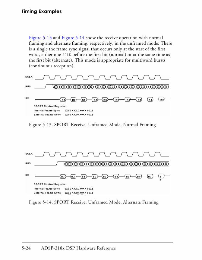
Timing Examples
Figure 5-13 and Figure 5-14 show the receive operation with normal framing and alternate framing, respectively, in the unframed mode. There is a single the frame sync signal that occurs only at the start of the first word, either one SCLK before the first bit (normal) or at the same time as the first bit (alternate). This mode is appropriate for multiword bursts (continuous reception).
SCLK
RFS
DRB3 B2 B1 B0 B3 B2 B1 B0 B2B3
SPORT Control Register:
Internal Frame Sync 0X 00 XXX 1 X0XX 0011
External Frame S ync 0X 00 XXX 0 X0XX 0011
Figure 5-13. SPORT Receive, Unframed Mode, Normal Framing
SCLK
RFS
DRB3 B2 B1 B0 B3 B2 B1 B0 B
2B3
SPORT Control Register:
Internal Frame Sync 0X01 XXX 1 X0XX 0011
External Frame S ync 0X01 XXX 0 X0XX 0011
Figure 5-14. SPORT Receive, Unframed Mode, Alternate Framing
5-24 ADSP-218x DSP Hardware Reference

Serial Ports
Figures 5-15 through 5-20 show framing for transmitting data and are very similar to Figures 5-9 to 5-14. In Figure 5-15 and Figure 5-16, the normal framing mode is shown for noncontinuous data and continuous data. Figure 5-17 and Figure 5-18 show noncontinuous and continuous transmission in the alternate framing mode. As with receive timing, the TFS output meets the TFS input timing requirement.
0XXX 1
B2 B1 B0
SCLK
OUTPUTTFS
DT
TFSINPUT
B3 B2 B1 B0B3
SPORT Control Register:
Internal Frame Sync 0XXX 101X 0XXX 0011
External Frame S ync 0 0X 0XXX 0011
Both Internal Framing Option and External Framing Option Shown
Figure 5-15. SPORT Transmit, Normal Framing
B2 B1 B0
SCLK
OUTPUTTFS
DT
TFSINPUT
B3 B2 B1 B0B3 B3 B2
SPORT Control Register:
Internal Frame Sync 0XXX 101X 0XXX 0011
External Fram e Sync 0XXX 100X 0XXX 0011
Both Internal Framing Option and External Framing Option Shown
Figure 5-16. SPORT Continuous Transmit, Normal Framing
ADSP-218x DSP Hardware Reference 5-25

Timing Examples
SCLK
TFS
DTB2 B1 B0B3 B2 B1 B0B3
TFS
OUTPUT
INPUT
SPORT Control Register:
Internal Frame Sync 0XXX 111X 0XXX 0011External Fram e Sync 0XXX 110X 0XXX 0011
Both Internal Framing Option and External Framing Option Shown
Note: There is an asynchronous delay between TFS input and DT. See the appropriate
data sheet for specifications.
Figure 5-17. SPORT Transmit, Alternate Framing
SCLK
OUTPUTTFS
DT
TFSINPUT
B2 B1 B0B3 B0B3 B2 B1
SPORT Control Register:Internal Frame Syn c 0XXX 111X 0XXX 0011
External Frame S ync 0XXX 110X 0XXX 0011
Both Internal Framing Option and External Framing Option Shown
Note: There is an asynchronous delay between TFS input and DT. See the appropriate
data sheet for specifications.
Figure 5-18. SPORT Continuous Transmit, Alternate Framing
5-26 ADSP-218x DSP Hardware Reference

Serial Ports
Figures 5-19 and 5-20 show the transmit operation with normal framing and alternate framing, respectively, in the unframed mode. There is a sin-gle the frame sync signal that occurs only at the start of the first word, either one SCLK before the first bit (normal) or at the same time as the first bit (alternate).
SCLK
TFS
DTB3 B3B0B1B2 B1 B0 B3B2 B2
SPORT Control Register:Internal Frame Sync 0XXX 001X 0XXX 0011External Fram e Sync 0XXX 000X 0XXX 0011
Figure 5-19. SPORT Transmit, Unframed Mode, Normal Framing
SCLK
TFS
DT B3 B3B0B1B2 B1 B0 B3B2 B2
SPORT Control Register:Internal Frame Syn c 0XXX 011X 0XXX 0011
External Frame Sync 0XXX 010X 0XXX 0011
Note: There is an asynchronou s delay between TFS input and DT. See the appropriate
data sheet fo r specifications.
Figure 5-20. SPORT Transmit, Unframed Mode, Alternate Framing
ADSP-218x DSP Hardware Reference 5-27
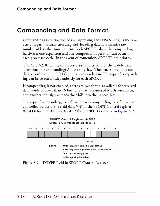
Companding and Data Format
Companding and Data FormatCompanding (a contraction of COMpressing and exPANDing) is the pro-cess of logarithmically encoding and decoding data to minimize the number of bits that must be sent. Both SPORTs share the companding hardware; one expansion and one compression operation can occur in each processor cycle. In the event of contention, SPORT0 has priority.
The ADSP-218x family of processors supports both of the widely used algorithms for companding: A-law and µ-law. The processor compands data according to the ITU G.711 recommendation. The type of compand-ing can be selected independently for each SPORT.
If companding is not enabled, there are two formats available for received data words of fewer than 16 bits: one that fills unused MSBs with zeros, and another that sign-extends the MSB into the unused bits.
The type of companding, as well as the non-companding data format, are controlled by the DTYPE field (bits 5-4) in the SPORT Control register (0x3FF6 for SPORT0 and 0x3FF2 for SPORT1) as shown in Figure 5-21.
SPORT0 Control Register: 0x3FF6
SPORT1 Control Register: 0x3FF2
DTYPE 00=Right justify, zero fill unused MSBs
01=Right justify, sign extend into unused MSBs
10=Compand using µ-law
11=Compand using A-law
15 14 13 12 11 10 9 8 7 6 5 4 3 2 1 0
Figure 5-21. DTYPE Field in SPORT Control Register
5-28 ADSP-218x DSP Hardware Reference

Serial Ports
When companding is enabled, valid data in the RX0 or RX1 register is the right-justified, sign-extended, expanded value of the eight LSBs received. Likewise, a write to TX0 or TX1 causes the 16-bit value to be compressed to eight LSBs (sign-extended to the width of the transmit word) before being written to the internal transmit register. If the magnitude of the 16-bit value is greater than the 13-bit A-law or 14-bit µ-law maximum, the value is automatically compressed to the maximum positive or negative value.
Companding Operation ExampleWith hardware companding, interfacing to a codec requires little addi-tional programming effort. See the codec hardware interfacing example in the last section of this chapter.
Here is a typical sequence of operations for transmitting companded data:
• Write data to the TXn register
• The value in TXn is compressed
• The compressed value is written back to TXn
• After the frame sync signal has occurred (if required), TXn is written to the internal transmit register and the bits are sent, MSB first.
As soon as the SPORT has started to send the second bit of the current word, TXn can be written with the next word, even though transmission of the first is not complete. After the MSB has been transferred, the SPORT generates the transmit interrupt to indicate that TXn is ready for the next data word. If the framing signal is being provided externally, the next word must be written to TXn early enough to allow for compression before the next framing signal arrives.
ADSP-218x DSP Hardware Reference 5-29

Companding and Data Format
Here is a typical sequence of operations for receiving companded data:
• Bits accumulate as received in the internal receive register
• When a complete word is received, it is written to RXn
• The value in RXn is expanded
• The expanded value is written back to RXn
The receive interrupt for that SPORT is then generated.
Contention for Companding HardwareSince both SPORTs share the companding hardware, only one compres-sion and one expansion operation can take place during a single machine cycle. If contention arises, such as when two expansions need to occur in the same cycle, SPORT0 has priority, while SPORT1 is forced to wait one cycle.
The effects of contention, however, are usually small. The instruction set does not support loading both TX0 and TX1 in the same cycle; conse-quently these operations will be naturally out of phase for contention in many cases. The overhead cycle for the receive operation occurs prior to the receive interrupt and does not increase the time needed to service the interrupt, although it does affect the latency prior to receiving the interrupt.
5-30 ADSP-218x DSP Hardware Reference

Serial Ports
Companding Internal DataBecause the values in the RX and TX registers are actually companded in place, it is possible to use the companding hardware internally, without any transmission or reception at all and without enabling the serial port. This operation can be used for debugging or data conversion and requires a single cycle of overhead.
To compress data, enable companding and then:
1. Write data to TXn (compression is calculated).
2. Wait for one cycle (TXn is written with compressed value)
3. Read TXn (it returns the 8-bit compressed data)
The code might look like this:
TX0 = AX0; /* linear data written to transmit register */NOP; /* any instruction */AX1 = TX0; /* compressed data transferred to AX1 */
Use the same procedure to expand data, but use RXn instead of TXn.
RX0 = AX0; /* compressed data written to receiveregister */
NOP; /* any instruction */AX1 = RX0; /* expanded - linear value transferred to
AX1 */
ADSP-218x DSP Hardware Reference 5-31

Autobuffering
AutobufferingIn normal operation, a SPORT generates an interrupt when it has received or has started to transmit a data word. Autobuffering provides a mecha-nism for receiving or transmitting an entire block of serial data before an interrupt is generated. Service routines can operate on the entire block of data, rather than on a single word, reducing overhead significantly. Auto-buffering is available on both SPORT0 and SPORT1.
Autobuffering uses the circular buffer addressing capability of the DAGs. With autobuffering enabled, each serial data word is transferred (or if multichannel operation is enabled, each active word is transferred) to or from Data Memory in a single overhead cycle. (Autobuffering to Program Memory is not supported.) This overhead cycle occurs independently of the instructions being executed and effectively suspends execution for one cycle (or more, if wait states are required) when it happens. No interrupt is generated for these individual data word transfers.
The autobuffer transfer cannot be duplicated by any instruction. How-ever, an equivalent assembly language instruction would be:
DM(I,M) = RX0or Equivalent Instructions Only
TX0 = DM(I,M)
The I and M registers used in the transfer are selected by fields in the SPORT’s Autobuffer Control register.
The processor waits for the current instruction to finish before inserting the overhead cycle. A delay in the autobuffer transfer occurs if the transfer is required during an instruction executing in multiple cycles (for wait states, for example). If the transfer is required when the processor is wait-ing in an IDLE state, the transfer is executed and the processor returns to IDLE.
5-32 ADSP-218x DSP Hardware Reference

Serial Ports
When a data word transfer causes the circular buffer pointer to wrap around, the SPORT interrupt is generated. The receive interrupt occurs after the complete buffer has been received. The transmit interrupt occurs when the last word is loaded into TXn, prior to transmission.
Aside from the completion of an instruction requiring multiple cycles and IDMA and BDMA cycles, the automatic transfer of individual data words has the highest priority of any operation short of RESET, including all interrupts. (For more information on the priority chain hierarchy of the ADSP-218x family, please see “Priority Chain” in Chapter 9, “DMA Ports.”) Thus, it is possible for an autobuffer transfer to increase the latency of an interrupt response if the interrupt happens to coincide with the transfer. Up to four autobuffered transfers can occur; in the case that two or more are needed in the same cycle, they have the following priority, which is the same as the SPORT interrupt priority:
Highest SPORT0 TransmitSPORT0 Receive
SPORT1 TransmitLowest SPORT1 Receive
In the worst case that all four autobuffer transfers are required at about the same time, interrupt latency would increase by the time it takes for all the transfers to occur, which is affected by wait states and bus request.
ADSP-218x DSP Hardware Reference 5-33

Autobuffering
Autobuffer Control RegisterIn autobuffering mode, an interrupt is generated when the modification of a specified I register (in the DAG) by the value in the specified M register (in the DAG) causes a modulus overflow (pointer wraparound). This means that the end of the buffer has been detected.
The autobuffering mode is enabled separately for receiving and transmit-ting by bits in the SPORT Autobuffer Control register (0x3FF3 for SPORT0 or 0x3FEF for SPORT1), shown in Figure 5-22.
The I and M registers used for autobuffering are identified by fields in the Autobuffer Control register. TIREG and TMREG are binary values that indicate the numbers of the I and M registers, respectively, associated with the transmit buffer. The rules governing the pairing of I and M registers are the same as for other DAG operations: the I and M registers must be in the same DAG, numbered either 0-3 for DAG1 or 4-7 for DAG2. Conse-quently, three bits identify the I register, but only two bits are necessary to indicate the M register because the third bit (MSB) of the M register number must be the same as for the I register.
TBUF
(Transm it Autobuffering Enable)
RBUF
(Receive Autobuffering Enable)
TIREG TMREG RIREG RMREG
SPORT0 Autobuffer Control Register: 0x3FF3
SPORT1 Autobuffer Control Register: 0x3FEF
15 14 13 12 11 10 9 8 7 6 5 4 3 2 1 0
Figure 5-22. SPORT Autobuffer Control Register
5-34 ADSP-218x DSP Hardware Reference

Serial Ports
Likewise, RIREG and RMREG indicate the numbers of the I and M regis-ters, respectively, associated with the receive buffer.
The TBUF and RBUF bits enable transmit autobuffering and receive auto-buffering, respectively. These bits are cleared to zeros at reset and after a reboot. Consequently, autobuffering in progress cannot continue through a reboot operation; you must re-enable autobuffering after a reboot.
Serial Port Autobuffering on the ADSP-2187/2188/2189 Processors
Due to the additional on-chip hardware memory overlay pages for all ver-sions of the ADSP-2187, ADSP-2188, and ADSP-2189 processors, special care must be taken when using autobuffering with these memory overlay pages. The autobuffering mechanism of the serial ports use the DAG reg-isters to control the target memory location. Just like normal DAG operations, autobuffering operations perform accesses to the hardware overlay currently pointed to by the PMOVLAY/DMOVLAY register.
For example, if you are autobuffering to Data Memory in the address range of 0x0000 through 0x1fff, then the DMOVLAY register controls the destination of the data. Changing the value of the overlay register could result in undesirable behavior, such as, scattering your data across multiple overlay pages.
However, if you take care in your program to only switch overlays on “wrap around” of the circular buffer’s Index register, you could have two or more buffers that you can use in a “ping-pong” fashion. These buffers reside at identical addresses on separate overlay regions. For more infor-mation on overlays, see Chapter 8, “Memory Interface.”
ADSP-218x DSP Hardware Reference 5-35

Autobuffering
Autobuffering ExampleListing 5-2 provides an example that sets up SPORT1 for autobuffering operation. The code assumes that the processor is running with a clockout frequency of 73.728 MHz. The SPORT will automatically transmit values from the circular buffer named tx_buffer. It will receive values as they are sent to the SPORT and automatically transfer the data into the buffer named rx_buffer. A transmit interrupt will be generated once all of the tx_buffer values have been transferred to TX1, but before the last value has been loaded into the transmit shift register. A receive interrupt will be generated once the rx_buffer has been completely filled.
Listing 5-2. Autobuffering Example Configuration Code
/* Initialization code for autobuffer */
.SECTION/DM data1;
.VAR/CIRC tx_buffer[10];
.VAR/CIRC rx_buffer[10];
.SECTION/PM program;
.global sport1_inits;
/* set up I,M, and L registers */
sport1_inits:I0 = tx_buffer; /* I0 contains address of
tx_buffer */M0 = 1; /* fill every location */L0 = length (tx_buffer);/* L0 set to length of
tx_buffer */I1 = rx_buffer; /* I1 points to
rx_buffer */L1 = length (rx_buffer);/* L1 set to length of
rx_buffer */
5-36 ADSP-218x DSP Hardware Reference

Serial Ports
/* set up SPORT1 for autobuffering */
AX0 = 0x0013; /* TX uses I0, M0;RX uses I1, M0 */
DM(0x3FEF) = AX0; /* autobuffering enabled */
/* set up SPORT1 for 8 kHz sampling and 2.048 MHz SCLK */
AX0 = 255; /* set RFSDIV to 255 for8 kHz */
DM(0x3FF0) = AX0;AX0 = 17; /* set SCLKDIV to 17 for
2.048 MHz SCLK */DM(0x3FF5) = AX0;
/* set up SPORT1 for normal required framing, internal SCLKinternal generated framing */
AX0 = 0x6B27; /* normal framing,8 bit mu-law */
DM(0x3FF2) = AX0; /* internal clock,framing */
/* set up interrupts */
IFC = 6; /* clear any extraneousSPORT interrupts*/
ICNTL = 0; /* interrupt nestingdisabled */
IMASK = 6; /* enable SPORT1interrupts */
/* enable SPORT1 */
AX0 = 0x0C1F; /* enable SPORT1 leave */DM(0x3FFF) = AX0; /* PWAIT, BWAIT as
default */
/* Place first transfer value into TX1 */
AX0 = DM(I0,M0);TX1 = AX0;RTS;
ADSP-218x DSP Hardware Reference 5-37

Multichannel Function
Multichannel FunctionSPORT0 supports a multichannel function. In the multichannel mode of operation, serial data is time-division multiplexed. Each subsequent word belongs to the next consecutive channel so that, for example, a 24-word block of data contains one word for each of 24 channels. SPORT0 sup-ports 32 or 24 channels and can automatically select words for particular channels while ignoring the others.
In single-channel mode, receive and transmit framing identifies the start of a single word or continuous stream, with independent receive and transmit operation. In the multichannel mode, the receive frame sync sig-nal (RFS0) identifies the start of a 24- or 32-word block of serial data with the receiver and transmitter operating in parallel. TFS0 has an alternate function, described in the following sections.
5-38 ADSP-218x DSP Hardware Reference

Serial Ports
Multichannel SetupMultichannel operation is enabled by bit 15 in SPORT0’s Control regis-ter (0x3FF6). When this bit is a 1, multichannel mode is enabled, and some control bits in the SPORT0 Control register are redefined. Bits affected by multichannel mode are shown in Figure 5-23. At reset, bit 15 is cleared, disabling multichannel mode and enabling normal operation.
The state of the multichannel length bit MCL, bit 9, determines whether there are 24 or 32 channels, i.e. whether the block length is 24 or 32 words. A 0 selects 24-word blocks; a 1, 32-word blocks. In multichannel mode, the word length is still set by the SLEN field in the SPORT Control register and can be 3 to 16 bits.
SPORT0 C ontrol R egiste r (M ultichannel Version)
0x3FF6
M CE
(M ultichanne l Enable)
1 = M ultich annel O pera tion
M CL (M ultichann el Length)
0 = 24 W o rds
1 = 32 W o rds
M FD
(M ultichannel
Fram e Delay)
INVTDV (Invert Transm it D ata Va lid )
15 14 13 12 11 10 9 8 7 6 5 4 3 2 1 0
1
Figure 5-23. SPORT0 Control Register with Multichannel Mode Enabled
ADSP-218x DSP Hardware Reference 5-39

Multichannel Function
The multichannel frame delay (MFD) is a 4-bit field specifying (in binary) the number of serial clock cycles between the frame sync signal and the first data bit. This allows the processor to work with different types of T1 interface devices. Figure 5-24 shows a variety of delays.
SCLK
FIRSTBIT
RFS M FD=9
RFS M FD=8
RFS M FD=7
RFS M FD=6
RFS M FD=5
RFS M FD=1
RFS M FD=0
9 8 7 6 5 4 3 2 1
Figure 5-24. SPORT Multichannel Frame Delay Examples
5-40 ADSP-218x DSP Hardware Reference

Serial Ports
The memory-mapped receive enable register and transmit enable register are each 32 bits wide and made up of two contiguous 16-bit registers, as shown in Figure 5-25. Each bit corresponds to a channel; setting the bit enables that channel so that the processor will select its word from the 24- or 32-word block. For example, setting bit 0 selects word 0, bit 12 selects word 12, and so on.
Multichannel OperationReceived words for channels that are not enabled are ignored; that is, no interrupts are generated for these words, no autobuffering occurs and no data is written to the RX0 register. Likewise, there are no interrupts and no autobuffering for transmit words that are not enabled. During transmit word time slots for channels that are not enabled, the data transmit (DT) pin is tristated.
1 = Channel Enabled
0 = Channel Ignored
31 30 29 28 27 26 25 24 23 22 21 20 19 18 17 16
15 14 13 12 11 10 9 8 7 6 5 4 3 2 1 0
31 30 29 28 27 26 25 24 23 22 21 20 19 18 17 16
15 14 13 12 11 10 9 8 7 6 5 4 3 2 1 0
Receive
Word
Enables
Transmit
Word
Enables
0x3FFA
0x3FF9
0x3FF8
0x3FF7
Figure 5-25. SPORT0 Multichannel Word Enable Registers
ADSP-218x DSP Hardware Reference 5-41

Multichannel Function
Most aspects of SPORT0 operate normally in the multichannel mode. Specifically, word length (SLEN), internal or external framing (IRFS), frame signal inversion (INVRFS), companding (DTYPE) and autobuffering are unchanged in the multichannel mode.
! It is important that RFS does not occur more than once per frame in multichannel mode.
Instead of providing frame synchronization, the TFS0 signal functions as a transmit data valid (TDV) signal in multichannel mode. TDV is asserted while the transmitter is active. TDV can be active high or low, and its polar-ity is controlled by the INVTFS bit, renamed INVTDV in this context. If INVTDV is a 1, TDV is active low; otherwise it is active high. TDV can be used to enable additional buffer logic, if required.
Figure 5-26 shows the start of a multichannel transfer. As in earlier exam-ples, word length is four bits (SLEN=3) and frame sync signals are active high. Multichannel frame delay (MFD) is one SCLK cycle. For the purpose of illustration, words 0 and 2 are selected for receiving and words 1 and 2 are selected for transmission.
SCLK
B3 B2 B1 B2DR
RFS
B0 IGNORED B3
DTB2B3 B0 B3 B2B1
TDV
WORD 0 WORD 1 WORD 2
Figure 5-26. Start of Multichannel Transfer
5-42 ADSP-218x DSP Hardware Reference
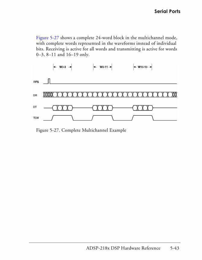
Serial Ports
Figure 5-27 shows a complete 24-word block in the multichannel mode, with complete words represented in the waveforms instead of individual bits. Receiving is active for all words and transmitting is active for words 0–3, 8–11 and 16–19 only.
Figure 5-27. Complete Multichannel Example
ADSP-218x DSP Hardware Reference 5-43

SPORT Timing Considerations
SPORT Timing ConsiderationsThe SPORTs support full duplex operation and are normally interrupt driven. That is, whenever a SPORT transaction has completed, the pro-cessor generates an internal interrupt. Under most operating conditions, the actual timing of the SPORT interrupts is not critical. In some sophis-ticated DSP systems, however, it is important to know the timing of the interrupt relative to the operation of the serial port.
Companding DelayUse of the companding circuit introduces latency in two ways. First, com-pressing or expanding a data value takes a single processor cycle. Second, SPORT0 has priority over SPORT1 if both require an expansion or com-pression operation in the same cycle; in this case, SPORT1 must wait one processor cycle. See the section on companding earlier in this chapter for more details on companding.
Clock Synchronization DelaySome SPORT timings depend on the processor clock. Other timings depend on the serial clock (SCLK0 or SCLK1). These clocks are asynchro-nous. There is a delay associated with synchronizing the serial clock to the processor clock whether the serial clock is internally or externally gener-ated. This delay is different for the transmit and receive interrupts, as explained in the following sections:“Transmit Interrupt Timing” on page 5-47 and “Receive Interrupt Timing” on page 5-48.
5-44 ADSP-218x DSP Hardware Reference

Serial Ports
Startup Timing
When a serial port is enabled by a write to the System Control register, it takes two SCLK cycles before it is actually enabled. On the next (third) SCLK cycle, the serial port becomes active, looking for a frame sync.
When the a serial port is disabled, if you set up the configuration to gener-ate an internal SCLK, the pin becomes active before the port is enabled.
Internally Generated Frame Sync TimingWhen internally generated frame syncs are used, all that is necessary to transmit data, from the programmer’s point of view, is to move the data into the appropriate TX register with an instruction such as:
TX0 = AX0;
Once data is written into the TX register, the processor generates a frame sync after a synchronization delay. This delay in turn affects the timing of the serial port transmit interrupt. The latency depends on five factors:
• Frequency of the serial clock
• Whether or not companding is enabled
• Whether or not there is contention for the companding circuit
• Whether the current word has finished transmitting
• Logic level of the SCLK when the data value was loaded into the transmit register
! If the transmit frame sync is generated externally, data starts trans-mitting when a frame sync signal is received.
ADSP-218x DSP Hardware Reference 5-45

SPORT Timing Considerations
After the TX register is loaded, it takes three complete phases of the serial clock, HIGH, LOW and HIGH, in that order, to ensure synchronization. See Figure 5-28.
Serial C lock
TX Written
Processor Clock
High Low High
MSB Transm itted(Alternate Framing)
Serial C lock
Processor Clock
High High
TX Written, SCLK High
TX Written, S CLK Low
TX Written
TFS OUTPUT(Normal Fram ing)
TFS OUTPUT(Alternate Framing)
TFS OUTPUT(Normal Fram ing)
TFS OUTPUT(Alternate Framing)
MSB Transm itted(Normal Fram ing)
MSB Transm itted(Alternate Framing)
MSB Transm itted(Normal Fram ing)
Low
Figure 5-28. Serial Clock Synchronization
5-46 ADSP-218x DSP Hardware Reference

Serial Ports
Once synchronization has been ensured and a frame sync generated, the most significant bit of the transmit word is shifted out as follows: on the same rising edge as the frame sync if alternate framing is used and on the rising edge of the next serial clock if normal framing is used. Therefore, the worst-case synchronization delay is two SCLK cycles.
There is additional delay if the previous data transmission has not com-pleted; the TX register cannot be loaded into the transmit shift register until the previous transmission is complete.
Transmit Interrupt TimingOnce the MSB has been transmitted, the subsequent bits are transmitted on the rising edges of the SCLK. The transmit interrupt (or autobuffer request) is generated internally on the falling edge of SCLK during the transmission of the second bit (see Figure 5-29). This timing gives the program time to load the TX register with the next data for continuous data transmission.
The transmit interrupt, like any other interrupt, must be synchronized to the processor clock. Servicing is subject to the same latencies as other interrupts. The transmit interrupt essentially means that it is all right to write a value to the TX register.
Interrupt or Autobuffer Request
TFS
DT
SCLK
BIT3 BIT2 BIT1 BIT0
Figure 5-29. SPORT Interrupt or Autobuffer Timing, Transmit 4-Bit Words (No Companding)
ADSP-218x DSP Hardware Reference 5-47
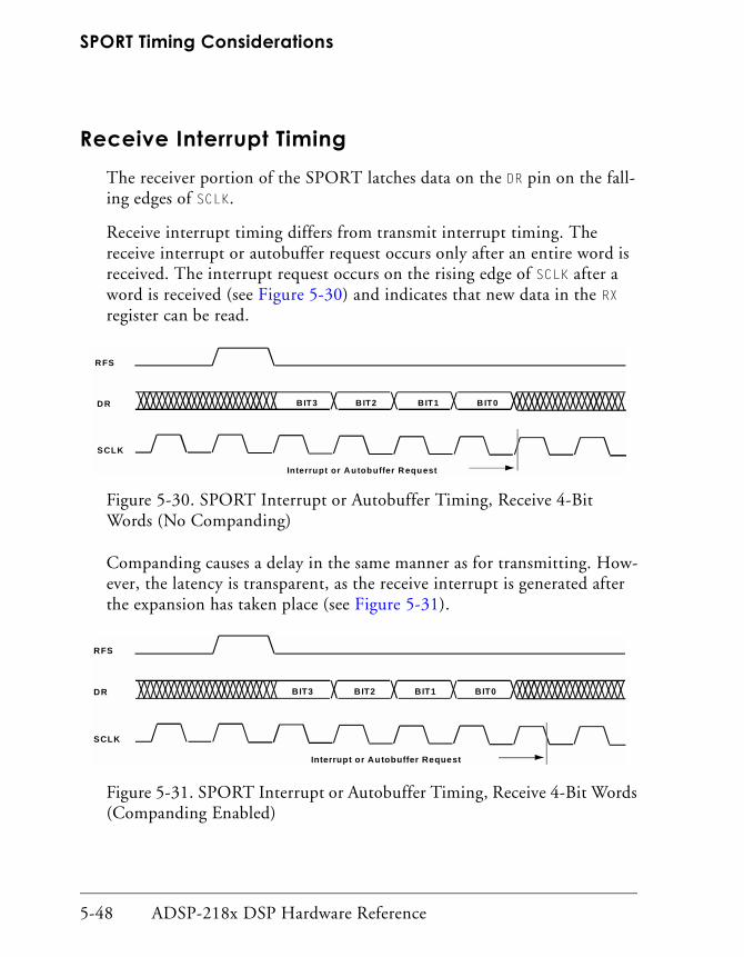
SPORT Timing Considerations
Receive Interrupt Timing The receiver portion of the SPORT latches data on the DR pin on the fall-ing edges of SCLK.
Receive interrupt timing differs from transmit interrupt timing. The receive interrupt or autobuffer request occurs only after an entire word is received. The interrupt request occurs on the rising edge of SCLK after a word is received (see Figure 5-30) and indicates that new data in the RX register can be read.
Companding causes a delay in the same manner as for transmitting. How-ever, the latency is transparent, as the receive interrupt is generated after the expansion has taken place (see Figure 5-31).
Interrupt or Autobuffer Request
RFS
DR
SCLK
BIT3 BIT2 BIT1 BIT0
Figure 5-30. SPORT Interrupt or Autobuffer Timing, Receive 4-Bit Words (No Companding)
Interrupt or Autobuffer Request
RFS
DR
SCLK
BIT3 BIT2 BIT1 BIT0
Figure 5-31. SPORT Interrupt or Autobuffer Timing, Receive 4-Bit Words (Companding Enabled)
5-48 ADSP-218x DSP Hardware Reference

Serial Ports
The LSB is received on the falling edge of SCLK. One processor cycle elapses to allow synchronization to the processor clock. One processor cycle later, the SPORT attempts to expand the data if companding is enabled and the other serial port is not using the companding circuitry. Companding latencies as discussed above occur prior to generation of a receive interrupt. Servicing the receive interrupt is subject to the same latencies as other interrupts.
Interrupt and Autobuffer SynchronizationThe serial ports are treated as an asynchronous system to the processor, even if the processor is providing the serial clock. Internal to the processor is a circuit which synchronizes the autobuffer or interrupt requests to the processor clock. Figure 5-32 shows the synchronization delay for the serial ports, assuming the setup and hold times are met for the current processor cycle. The setup and hold times for the serial port requests are the same as shown on the data sheet for the IRQ2 signal. If the setup and hold times are not met, there is an additional processor cycle of delay added.
As shown in Figure 5-32, there is a two-processor-cycle delay before the autobuffer or interrupt request is acted on by the processor. The same latencies exist for all external interrupts. The processor can only service interrupt or autobuffer requests on instruction cycle boundaries, so there may be additional latency cycles added due to the completion of an instruction.
Processor can service the request here
CLKOUT
Request
Setup Time
Hold Time
Figure 5-32. Synchronization of Autobuffer or Interrupt Request to Pro-cessor Clock
ADSP-218x DSP Hardware Reference 5-49

SPORT Timing Considerations
Instruction Completion LatenciesThere are several situations which can cause an instruction to take more than one processor cycle. Any of the following can delay the processor’s ability to service a pending interrupt or autobuffer request:
• External memory wait states
• Bus request when an external access is required (in Go mode)
• Bus request with Go mode disabled
• Multiple external accesses required for a single instruction
• A pending higher priority autobuffer or interrupt request
• Interrupt being masked
On instruction cycle boundaries the processor will service multiple pend-ing interrupt or autobuffer requests in the following priority order:
• SPORT0 transmit autobuffer—highest priority
• SPORT0 receive autobuffer
• SPORT1 transmit autobuffer
• SPORT1 receive autobuffer
• Unmasked pending interrupts in priority order
5-50 ADSP-218x DSP Hardware Reference

Serial Ports
Interrupt and Autobuffer Service ExampleFigure 5-33 shows the execution of a serial port interrupt based on a request that meets the setup and hold time requirements. This example is the same for a receive or a transmit interrupt request.
An additional latency cycle is consumed due to the fetching of the first instruction of the interrupt routine. The interrupt can only be serviced on an instruction cycle boundary. The above example (in Figure 5-33) assumes all instructions are completed in one processor cycle. Figure 5-34 shows the result of an autobuffer request that meets the setup and hold requirements.
Request
CLKOUT
EXEC A B FETCH INT INT
Sync Delay
NOP Instruction, Fetch Vector
Execute first instruction of interrupt routine
Figure 5-33. Interrupt Service Example
Request
CLKOUT
EXEC A B AUTOBUFFER C
Sync Delay
Do the autobuffer transfer
Continue main program
Figure 5-34. Autobuffer Service Example
ADSP-218x DSP Hardware Reference 5-51
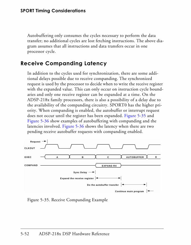
SPORT Timing Considerations
Autobuffering only consumes the cycles necessary to perform the data transfer; no additional cycles are lost fetching instructions. The above dia-gram assumes that all instructions and data transfers occur in one processor cycle.
Receive Companding LatencyIn addition to the cycles used for synchronization, there are some addi-tional delays possible due to receive companding. The synchronized request is used by the processor to decide when to write the receive register with the expanded value. This can only occur on instruction cycle bound-aries and only one receive register can be expanded at a time. On the ADSP-218x family processors, there is also a possibility of a delay due to the availability of the companding circuitry. SPORT0 has the higher pri-ority. When companding is enabled, the autobuffer or interrupt request does not occur until the register has been expanded. Figure 5-35 and Figure 5-36 show examples of autobuffering with companding and the latencies involved. Figure 5-36 shows the latency when there are two pending receive autobuffer requests with companding enabled.
Request
CLKOUT
EXEC A B C AUTOBUFFER
Sync Delay
Expand the receive register
Do the autobuffer transfer
D
COMPAND EXPAND RX
Continue main program
Figure 5-35. Receive Companding Example
5-52 ADSP-218x DSP Hardware Reference

Serial Ports
Interrupts with Autobuffering EnabledWhen autobuffering is enabled, SPORT interrupts occur when the address modification done during the autobuffer operation causes a mod-ulus wraparound. The synchronization delay applies to this type of interrupt as well. An example is shown in Figure 5-37.
CLKOUT
EXEC
Sync Delay
Expand RX0
COMPAND
Continue main program
Request SPORT1 Receive
Request SPORT0 Receive
EXPAND RX0 EXPAND RX1
A B C AUTOBUFFE R DAUTOBUFFER
Expand RX1
RX0 Autobuffer Transfer
RX1 Autobuffer Transfer
Figure 5-36. Receive Companding Example with Both Serial Ports
CLKOUT
EXEC INTFETCH INTEAUTOBUFFER
Sync Delay
NOP Instruction, Fetch Vector
Execute first instruction of interrupt routine
D
Figure 5-37. Autobuffering Interrupt Example
ADSP-218x DSP Hardware Reference 5-53

SPORT Timing Considerations
Unusual ComplicationsIn most cases the serial port companding, autobuffer, and interrupt laten-cies are transparent to your application program. When trying to use the same I register for more than one autobuffer channel, it becomes impor-tant to make sure that the latencies do not affect the correct order of operations. For example, if the serial port data is continuous, and the receiver and transmitter are working with the same frame signal, the order of the transmit and receive autobuffer or interrupt operations may be affected by the latencies, as shown in Figure 5-38.
If the processor is free to handle the autobuffer requests in the order they are generated, the receive autobuffer happens first and is then followed by the transmit autobuffer. The order of these operations may change if the processor is not available to handle the requests due to any of the previ-ously mentioned latencies.
In the example shown in Figure 5-35, there are 1½ serial clock cycles between the requests. If the processor is subject to bus requests, wait states, or other latencies that are longer than 1½ serial clock cycles, both autobuffer operations may be held off. Since the transmit autobuffer has a higher priority, its request will occur first.
Transmit autobuffer request
SCLK
BIT3 BIT2 BIT1 BIT0 BIT3 BIT2 BIT1 BIT0
BIT3 BIT2 BIT1 BIT0 BIT3 BIT2 BIT1 BIT0
DR
DT
Receive autobuffer request
Figure 5-38. Using One Index Register for Transmit and Receive Autobuffer
5-54 ADSP-218x DSP Hardware Reference

Serial Ports
Because of the priority of the autobuffer requests, the use of a single I reg-ister is more difficult or even impossible in some cases. As long as there are no possible latency cases longer than the difference in the timing of the requests, it is quite possible to use a single I register for serial port autobuffering.
Serial Port Startup IssuesSerial clocks have some special startup issues that you need to be aware of and take precautions for. This section discusses these issues.
Gated Serial ClocksThe ADSP-218x family processors require two serial clock cycles to syn-chronize the enabling of the serial port to the serial clock signal. Therefore, Analog Devices recommends using a continuous serial clock for frame sync signals that are active for more than a single serial clock cycle. However, if a gated serial clock is used in your system with a frame sync signal that is longer than one serial clock cycle, you must use the fol-lowing procedure each time the serial port is enabled.
1. Set the SLEN in the SPORT Control register to be equal to (normal word length-2).
For example, if 12-bit words are being transmitted/received, set the SLEN field in the SPORTx Control register to 9 in the main part of the program that sets up the SPORT.
2. Enable the SPORT.
3. Ignore the first word transmitted/received.
4. When the interrupt service routine is serviced for the first time, change the value in the SLEN field back to 11 as you go. This change will cause the SPORT to re-synchronize and trans-mit/receive the correct words.
ADSP-218x DSP Hardware Reference 5-55
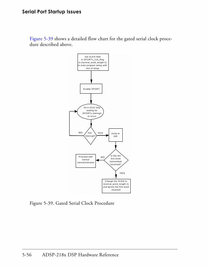
Serial Port Startup Issues
Figure 5-39 shows a detailed flow chart for the gated serial clock proce-dure described above.
Set SLEN fieldin SPORTx_Ctrl_Reg
to (normal_word_length-2)in main program along with
rest of setup
Sit in IDLE loopwaiting for
SPORTx interruptto occur
Get Interrupt?
NO YES
Enable SPORT
Jump toISR
NO
YES
Is this thefirst word
transmitted/received?
Proceed withnormal
transmit/receive
Change the SLEN to(norm al_word_length-1)and ignore the first word
received
Figure 5-39. Gated Serial Clock Procedure
5-56 ADSP-218x DSP Hardware Reference
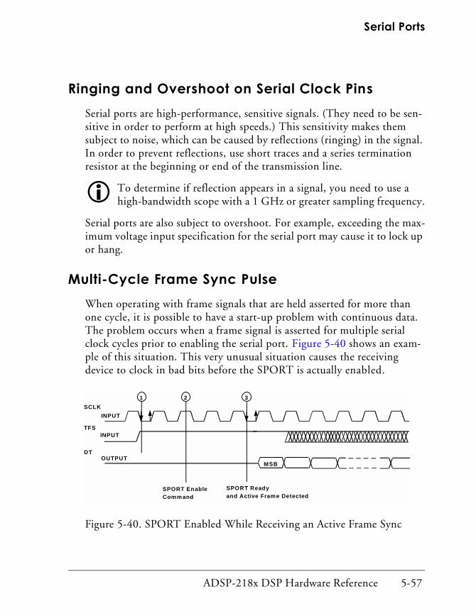
Serial Ports
Ringing and Overshoot on Serial Clock PinsSerial ports are high-performance, sensitive signals. (They need to be sen-sitive in order to perform at high speeds.) This sensitivity makes them subject to noise, which can be caused by reflections (ringing) in the signal. In order to prevent reflections, use short traces and a series termination resistor at the beginning or end of the transmission line.
! To determine if reflection appears in a signal, you need to use a high-bandwidth scope with a 1 GHz or greater sampling frequency.
Serial ports are also subject to overshoot. For example, exceeding the max-imum voltage input specification for the serial port may cause it to lock up or hang.
Multi-Cycle Frame Sync PulseWhen operating with frame signals that are held asserted for more than one cycle, it is possible to have a start-up problem with continuous data. The problem occurs when a frame signal is asserted for multiple serial clock cycles prior to enabling the serial port. Figure 5-40 shows an exam-ple of this situation. This very unusual situation causes the receiving device to clock in bad bits before the SPORT is actually enabled.
SCLK
TFS
DT
SPORT EnableCommand
1 2 3
MSB
INPUT
INPUT
OUTPUT
SPORT Readyand Active Frame Detected
Figure 5-40. SPORT Enabled While Receiving an Active Frame Sync
ADSP-218x DSP Hardware Reference 5-57

Serial Port Startup Issues
At position ② in Figure 5-40 the SPORT is being enabled. The SPORT takes the normal two SCLK cycle delay to become active, and at position ③ , it begins looking for the TFS signal. In this case, however, the TFS signal is already active and the receiving device already started receiving bits. This situation causes the receiving device to clock in some number of incorrect bits. There are three different cases to be concerned with:
• Non-continuous data—only the first received word is affected; the next word syncs properly
• Frame in multi-channel mode—the entire first frame is incorrect
• Continuous data—the entire data stream is misaligned
If this situation is likely to be a problem, the external circuit shown in Figure 5-41 can be used to disable the received frame sync until the SPORT is truly active. Disabling the received frame sync permits software to check the status of the frame sync and wait for it to become inactive before enabling the input.
SCLK
TFS
RFS
DR
DT
FLIN
FLOUT
SP
OR
T TFS
SCLK
RFS
DR
DT
Figure 5-41. External SPORT Enable Circuit
5-58 ADSP-218x DSP Hardware Reference

6 TIMERFigure 6-0.
Table 6-0.
Listing 6-0.
OverviewThe programmable interval timer can generate periodic interrupts based on multiples of the processor’s cycle time. When enabled, a 16-bit count register is decremented every n cycles, where n-1 is a scaling value stored in an 8-bit register. When the value of the count register reaches zero, an interrupt is generated and the count register is reloaded from a 16-bit period register.
The scaling feature of the timer allows the 16-bit counter to generate peri-odic interrupts over a wide range of periods. Given a processor cycle time of 80 ns, the timer can generate interrupts with periods of 80 ns up to 5.24 ms with a zero scale value. When scaling is used, time periods can range up to 1.34 seconds.
Timer interrupts can be masked, cleared and forced in software if desired. For additional information, refer to the section “Interrupts” in Chapter 3, “Program Control.”
ADSP-218x DSP Hardware Reference 6-1

Timer Architecture
Timer Architecture The timer includes two 16-bit registers, TCOUNT and TPERIOD and one 8-bit register, TSCALE. The extended Mode Control instruction enables and dis-ables the timer by setting and clearing bit 5 in the Mode Status register, MSTAT. For a description of the Mode Control instructions, refer to the ADSP-218x DSP Instruction Set Reference. The timer registers, which are memory-mapped, are shown in Figure 6-1.
TCOUNT is the count register. When the timer is enabled, it is decremented as often as once every instruction cycle. When the counter reaches zero, an interrupt is generated. TCOUNT is then reloaded from the TPERIOD register and the count begins again.
0x3FFD
0x3FFC
0x3FFB
TPERIOD Period Register
TCOUNT Counter Register
TSCALE Scaling Register00000000
1 5 1 4 1 3 1 2 1 1 1 0 9 8 7 6 5 4 3 2 1 0
Figure 6-1. Timer Registers
6-2 ADSP-218x DSP Hardware Reference

Timer
TSCALE stores a scaling value that is one less than the number of cycles between decrements of TCOUNT. For example, if the value in TSCALE register is 0, the counter register decrements once every cycle. If the value in TSCALE is 1, the counter decrements once every 2 cycles. Figure 6-2 shows the timer block diagram.
TSCALE TPERIOD
CLKOUTTimer Enable and
TCOUNTDecrement Zero
Count Register Load Logic
TimerInterrupt
Timer Enable
16
16
168
DMD Bus
Prescale Logic
Figure 6-2. Timer Block Diagram
ADSP-218x DSP Hardware Reference 6-3

Resolution
ResolutionTSCALE provides the capability to program longer time intervals between interrupts, extending the range of the 16-bit TCOUNT register. Table 6-1 shows the range and the relationship between period length and resolution for TPERIOD = maximum.
Timer Operation Table 6-2 shows the effect of operating the timer with TPERIOD = 5, TSCALE = 1 and TCOUNT = 5. After the timer is enabled (cycle n–1) the counter begins. Because TSCALE is 1, TCOUNT is decremented on every other cycle. The reloading of TCOUNT and continuation of the counting occurs, as shown, during the interrupt service routine.
Table 6-1. Timer Range and Resolution
Cycle Time = 30 ns
TSCALE Interrupt Every… Resolution
0 1.97 ms 30 ns
255 .5 s 7.65 µs
Table 6-2. Example Of Timer Operation
Cycle TCOUNT Action
n–4 TPERIOD loaded with 5
n–3 TSCALE loaded with 1
n–2 TCOUNT loaded with 5
6-4 ADSP-218x DSP Hardware Reference
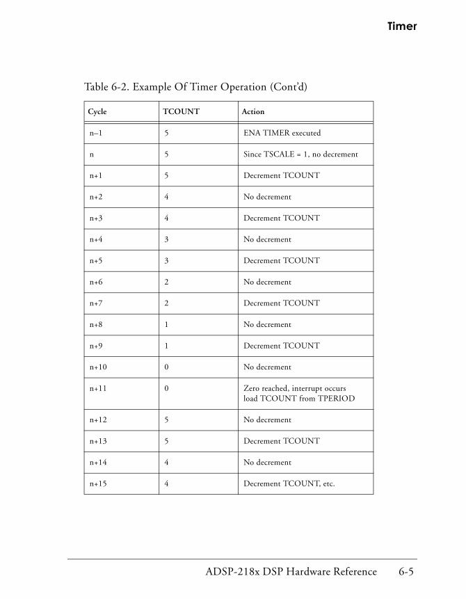
Timer
n–1 5 ENA TIMER executed
n 5 Since TSCALE = 1, no decrement
n+1 5 Decrement TCOUNT
n+2 4 No decrement
n+3 4 Decrement TCOUNT
n+4 3 No decrement
n+5 3 Decrement TCOUNT
n+6 2 No decrement
n+7 2 Decrement TCOUNT
n+8 1 No decrement
n+9 1 Decrement TCOUNT
n+10 0 No decrement
n+11 0 Zero reached, interrupt occursload TCOUNT from TPERIOD
n+12 5 No decrement
n+13 5 Decrement TCOUNT
n+14 4 No decrement
n+15 4 Decrement TCOUNT, etc.
Table 6-2. Example Of Timer Operation (Cont’d)
Cycle TCOUNT Action
ADSP-218x DSP Hardware Reference 6-5
Enabling the Timer
One interrupt occurs every (TPERIOD +1) * (TSCALE +1) cycles. To set the first interrupt at a different time interval from subsequent interrupts, load TCOUNT with a different value from TPERIOD. The formula for the first interrupt is (TCOUNT+1) * (TSCALE+1).
If you write a new value to TSCALE or TCOUNT, the change is effective imme-diately. If you write a new value to TPERIOD, the change does not take effect until after TCOUNT is reloaded.
Enabling the TimerThis section tells you how to enable the timer and generate interrupts. It lists the steps you need to use and provides sample code (see Listing 6-1).
To enable the timer:
1. Set values for TCOUNT, TPERIOD, and TSCALE.
2. Set bit 0 in IMASK to enable interrupt.
3. Execute ENA TIMER instruction to start counting down (bit 5 in MSTAT register).
Listing 6-1. Sample Code for Enabling the Timer and Generating Interrupts
#include <def2181.h>
.SECTION/PM interrupts;
/* ------Interrupt vector table------ */JUMP Start; NOP; NOP; NOP; /* reset vector */RTI; NOP; NOP; NOP; /* IRQ2 */RTI; NOP; NOP; NOP; /* IRQL1 */RTI; NOP; NOP; NOP; /* IRQL0 */RTI; NOP; NOP; NOP; /* SPORT0 transmit */RTI; NOP; NOP; NOP; /* SPORT0 receive */RTI; NOP; NOP; NOP; /* IRQE */
6-6 ADSP-218x DSP Hardware Reference

Timer
RTI; NOP; NOP; NOP; /* BDMA */RTI; NOP; NOP; NOP; /* SPORT1 transmit */RTI; NOP; NOP; NOP; /* SPORT1 receive */JUMP Interrupt_Hit; NOP; NOP; NOP; /* timer */
.SECTION/PM Program;Start:/* set TSCALE to decrement every cycle */AX0 = 0;DM(Tscale_Reg) = AX0;/* set TCOUNT to generate first interrupt at 50 cycles */AX0 = 49;DM(Tcount_Reg) = AX0;/* set TPERIOD to reload TCOUNT with 99 at interrupt */AX0 = 99;DM(Tperiod_Reg) = AX0;/* enable the timer interrupt */IMASK = 0x1;/* start the count down after executing this */ENA TIMER;
/* ------Wait for timer interrupt------------ */wait: IDLE; Jump wait;
Interrupt_Hit:RTI;
ADSP-218x DSP Hardware Reference 6-7
Enabling the Timer
6-8 ADSP-218x DSP Hardware Reference

7 SYSTEM INTERFACEFigure 7-0.
Table 7-0.
Listing 7-0.
OverviewThis chapter describes the basic system interface features of the ADSP-218x family processors. The system interface includes various hard-ware and software features used to control the DSP processor.
Processor control pins include a RESET signal, clock signals, flag inputs and outputs, and interrupt requests. This chapter describes only the logical relationships of control signals; consult individual processor data sheets for actual timing specifications.
Pin DescriptionsThis section provides functional descriptions of the ADSP-218x processor pins. Because processors come in different packages, there are some differ-ences in the pins contained on each. Table 7-1 shows the package configurations for each ADSP-218x processor and the sections that follow identify the pins for each package.
Table 7-1. ADSP-218x Processor Package Configurations
Processor Package
ADSP-2181 128-LQFP and 128-MQFP
ADSP-2183 128-LQFP and 144-Mini-BGA
ADSP-218x DSP Hardware Reference 7-1

Pin Descriptions
ADSP-2184 100-LQFP
ADSP-2184L1 100-LQFP
ADSP-2184N3 100-LQFP and 144-miniBGA
ADSP-2185 100-LQFP
ADSP-2185L1 100-Lead LQFP and 144-Mini-BGA
ADSP-2185M2 100-LQFP and 144-miniBGA
ADSP-2185N3 100-LQFP and 144-miniBGA
ADSP-2186 100-LQFP and 144-Mini-BGA
ADSP-2186L1 100-LQFP and 144-Mini-BGA
ADSP-2186M2 100-LQFP and 144-Mini-BGA
ADSP-2186N3 100-LQFP and 144-miniBGA
ADSP-2187L1 100-LQFP
ADSP-2187N3 100-LQFP and 144-miniBGA
ADSP-2188M2 100-LQFP and 144-Mini-BGA
ADSP-2188N3 100-LQFP and 144-miniBGA
Table 7-1. ADSP-218x Processor Package Configurations (Cont’d)
Processor Package
7-2 ADSP-218x DSP Hardware Reference

System Interface
Pin Descriptions for 128-LQFP Package ProcessorsUnlike the other ADSP-218x processors, the ADSP-2181 and ADSP-2183 processors come in 128-LQFP and 128-MQFP packages. For these two processors, the full address, data, and IDMA port signals are brought out to external pins. The remainder of the ADSP-218x proces-sors, which come in 100-LQFP packages, multiplex the address bus and a portion of the data bus to achieve a lower package pinout.
ADSP-2189M2 100-LQFP and 144-Mini-BGA
ADSP-2189N3 100-LQFP and 144-miniBGA
1 L indicates that the processor operates at 3.3 V. These processors are not tolerant to 5 V inputs
2 M indicates that the processor core operates at 2.5 V and that the external I/O can operate between 2.5 V and 3.3 V. The external I/O is tolerant to up to 3.6 V inputs with a supply voltage between 2.5 V and 3.3 V. However, it is not tolerant to 5 V inputs.
3 N indicates that the processor core operates at11.8 V and that the external I/O can operate between 1.8 V or 3.3 V. The external I/O is tolerant to up to 3.6 V inputs with a supply voltage of 1.8 V or 3.3 V. However, it is not tolerant to 5 V inputs.
Table 7-1. ADSP-218x Processor Package Configurations (Cont’d)
Processor Package
ADSP-218x DSP Hardware Reference 7-3
Pin Descriptions
Table 7-2 provides a description of the ADSP-2181 and ADSP-2183 pro-cessor pins. All pin descriptions also apply to the ADSP-2183 processor in the 144-Lead Mini-BGA package unless otherwise noted.
Table 7-2. ADSP-2181 and ADSP-2183 Processor Pin Descriptions
Pin Name(s) # of Pins
I/O Function
Address 14 O Address Output Pins for Program, Data, Byte, and I/O spaces
Data 24 I/O Data I/O Pins for Program and Data Memory Spaces (8 MSBs are also used as Byte Space Addresses
RESET 1 I Processor Reset Input
IRQ2 1 I Edge- or Level-Sensitive Interrupt Request
IRQL0
IRQL1
1
1
I
I
Level-Sensitive Interrupt Requests
IRQE 1 I Edge-Sensitive Interrupt Requests
BR 1 I Bus Request Input
BG 1 O Bus Grant Output
BGH 1 O Bus Grant Hung Output
PMS 1 O Program Memory Select Output
DMS 1 O Data Memory Select Output
BMS 1 O Byte Memory Select Output
IOMS 1 O Memory Select Output
7-4 ADSP-218x DSP Hardware Reference

System Interface
CMS 1 O Combined Memory Select Output
RD 1 O Memory Read Enable Output
WR 1 O Memory Write Enable Output
MMAP 1 I Memory Map Select Input
BMODE 1 I Boot Option Control Input
CLKIN
XTAL
2 I Clock or Quartz Crystal Input
CLKOUT 1 O Processor Clock Output
SPORT0 5 I/O Serial Port I/O Pins
SPORT1 5 I/O Serial Port1 or two external IRQs, Flag In and Flag Out
IRD
IWR
2 I IDMA Port Read/ Write Inputs
IS 1 I IDMA Port Select
IAL 1 I IDMA Port Address Latch Enable
IAD 16 I/O IDMA Port Address/Data Bus
IACK I O IDMA Port Access Ready
PWD 1 I Powerdown Control Input
PWDACK I O Powerdown Control Output
Table 7-2. ADSP-2181 and ADSP-2183 Processor Pin Descriptions (Cont’d)
Pin Name(s) # of Pins
I/O Function
ADSP-218x DSP Hardware Reference 7-5

Pin Descriptions
FL0, FL1, FL2 3 O Output Flags
PF7:0 8 I/O Programmable I/O Pins
EE 1 * Emulator only*
EBR 1 * Emulator only*
EBG 1 * Emulator only*
ERESET 1 * Emulator only*
EMS 1 * Emulator only*
EINT 1 * Emulator only*
ECLK 1 * Emulator only*
ELIN 1 * Emulator only*
ELOUT 1 * Emulator only*
Table 7-2. ADSP-2181 and ADSP-2183 Processor Pin Descriptions (Cont’d)
Pin Name(s) # of Pins
I/O Function
7-6 ADSP-218x DSP Hardware Reference
System Interface
Pin Descriptions for 100-LQFP Package ProcessorsIn order to maintain maximum functionality and reduce package size and pin count in the 100-LQFP packages, some serial port, programmable flag, interrupt, and external bus pins have dual, multiplexed functionality. The external bus pins are configured during RESET only, while serial port pins are software configurable during program execution.
VDD
GND
6
11
Power
Ground
(Applies to ADSP-2181 and ADSP-2183 in 128-LQFP package only)
VDD
GND
11
22
Power
Ground
(Applies to ADSP-2183 in 144-Lead Mini-BGA package only)
* These pins must be connected only to the EZ-ICE connector in the target system. These pins have no function except during emulation and do not require pull-up or pull-down resistors.
Table 7-2. ADSP-2181 and ADSP-2183 Processor Pin Descriptions (Cont’d)
Pin Name(s) # of Pins
I/O Function
ADSP-218x DSP Hardware Reference 7-7

Pin Descriptions
The programmable flag pins on the ADSP-218x 100-LQFP processors retain the same functionality as those on the ADSP-2181 and ADSP-2183 128-LQFP packages but share these pins with interrupt pins. The pro-grammable flag pins PF[7:4] are shared with interrupts IRQ2, IRQL1, IRQL0, and IRQE, respectively. Both the programmable flags and interrupts are directly connected to the shared pins. You use existing control registers to choose the desired function for each pin. Each pin has four possible states:
• IMASK[x]=0, PFTYPE[x]=0(PF Input)
• Read of PFDATA gives pin value
• No interrupt occurs
• Default after reset
• IMASK[x]=1, PFTYPE[x]=0(PF Input)
• Read of PFDATA gives pin value
• Interrupt occurs on level- or edge-transition
• IMASK[x]=0, PFTYPE[x]=1(PF Output)
• Write to PFDATA sets pin value
• Read of PFDATA gives set value
• No interrupt occurs
• IMASK[x]=1, PFTYPE[x]=1(PF Output)
• Write to PFDATA sets pin value and may cause interrupt (level- or edge-sensitive)
• Read of PFDATA gives set value
7-8 ADSP-218x DSP Hardware Reference

System Interface
After reset, the PF pins default to inputs and the interrupts are disabled by the IMASK register’s default value. The pins can be used as PF outputs by changing the PFTYPE register and leaving the interrupt disabled in IMASK. If the pins are to be used as interrupts, then the PFTYPE register need not be changed, but the interrupt must be enabled in the IMASK register.
Common-Mode Pins
Table 7-3 provides a description of the pins that are common to both Full Memory Mode and Host Memory Mode in 100-LQFP packages. In cases where pin functionality is reconfigurable, the default state is shown in plain text; alternate functionality is shown in italics. All pin descriptions also apply to the processors in 144-Ball Mini-BGA packages unless other-wise noted.
Table 7-3. Common-Mode Pins
Pin Name(s) Number of Pins
I/O Function
RESET 1 I Processor Reset Input
BR 1 I Bus Request Input
BG 1 O Bus Grant Output
BGH 1 O Bus Grant Hung Output
DMS 1 O Data Memory Select Output
PMS 1 O Program Memory Select Output
IOMS 1 O Memory Select Output
BMS 1 O Byte Memory Select Output
CMS 1 O Combined Memory Select Output
ADSP-218x DSP Hardware Reference 7-9

Pin Descriptions
RD 1 O Memory Read Enable Output
WR 1 O Memory Write Enable Output
IRQ2
PF7
1 I
I/O
Edge- or Level-Sensitive Interrupt Request1
Programmable I/O Pin
IRQL1
PF6
1 I
I/O
Level-Sensitive Interrupt Requests1
Programmable I/O Pin
IRQL0
PF5
1 I
I/O
Level-Sensitive Interrupt Requests1
Programmable I/O Pin
IRQE
PF4
1 I
I/O
Edge-Sensitive Interrupt Requests1
Programmable I/O Pin
Mode D
PF3
1 I
I/O
Mode Select Input - Checked only during RESET
Programmable I/O Pin during normal operation
Mode C
PF2
1 I
I/O
Mode Select Input - Checked only during RESET
Programmable I/O Pin during normal operation
Mode B
PF1
1 I
I/O
Mode Select Input - Checked only during RESET
Programmable I/O Pin during normal operation
Mode A
PF0
1 I
I/O
Mode Select Input - Checked only during RESET
Programmable I/O Pin during normal operation
CLKIN
XTAL
2 I Clock or Quartz Crystal Input
Table 7-3. Common-Mode Pins (Cont’d)
Pin Name(s) Number of Pins
I/O Function
7-10 ADSP-218x DSP Hardware Reference

System Interface
CLKOUT 1 O Processor Clock Output
SPORT0 5 I/O Serial Port I/O Pins
SPORT1
IRQ1:0, FI, FO
5 I/O Serial Port I/O Pins
Edge- or Level-Sensitive Interrupts, Flag In, Flag
Out2
PWD
PWDACK
FL0, FL1, FL2
1
I
3
I
O
O
Powerdown Control Input
Powerdown Control Output
Output Flags
VDD
GND
6
10
I
I
Power
Ground
(Applies to all ADSP-2184, ADSP-2184L, ADSP-2185, ADSP-2185L, ADSP-2186, ADSP-2186L, ADSP-2187L processors in 100-Lead LQFP package only)
VDD
GND
11
20
I
I
Power
Ground
(Applies to ADSP- 2185L, ADSP-2186, and ADSP- 2186L processors in 144-Mini-BGA package only)
VDDINT
VDDEXT
GND
2
4
10
I
I
I
Internal VDD (2.5V) Power
External VDD (2.5V or 3.3V) Power
Ground
(Applies to all ADSP-218x M and N series processors in 100-Lead LQFP package only)
Table 7-3. Common-Mode Pins (Cont’d)
Pin Name(s) Number of Pins
I/O Function
ADSP-218x DSP Hardware Reference 7-11

Pin Descriptions
Memory Mode PinsTable 7-4 provides a description of Full Memory Mode pins and Table 7-5 provides a description of the Host Memory Mode pins on ADSP-218x processors in 100-lead LQFP and 144-MBGA packages.
VDDINT
VDDEXT
GND
4
7
20
I
I
I
Internal VDD (2.5V) Power
External VDD (2.5V or 3.3V) Power
Ground
(Applies to all ADSP-218x M and N series processors in 144-Ball Mini-BGA package only)
EZ-Port 9 I/O For emulation use
1 Interrupt/Flag Pins retain both functions concurrently. If IMASK is set to enable the correspond-ing interrupts, then the DSP will vector to the appropriate interrupt vector address when the pin is asserted, either by external devices, or set as a programmable flag.
2 SPORT configuration determined by the DSP System Control register. Software configurable.
Table 7-4. Full Memory Mode Pins (Mode C = 0)
Pin Name Number of Pins
I/O Function
A13:0 14 O Address Output Pins for Program, Data, Byte and I/O Spaces
D23:0 24 I/O Data I/O Pins for Program, Data, Byte and I/O Spaces (8 MSBs are also used as Byte Memory addresses)
Table 7-3. Common-Mode Pins (Cont’d)
Pin Name(s) Number of Pins
I/O Function
7-12 ADSP-218x DSP Hardware Reference

System Interface
Active or Passive Mode Pin Configuration
To decrease the package size of the ADSP-218x family processors for the 100-LQFP packages, the IDMA bus and associated control signals are multiplexed with the external Address and Data busses. The logic value of the Mode pins are latched on the rising edge of the RESET signal. The val-ues of the Mode pins determine whether the DSP will boot from an EPROM or be booted from an external host processor.
The Mode pins also determine whether the DSP’s external pins are used for IDMA accesses (Host Memory mode) or whether the full 14-bit address bus and 24-bit data bus is active (Full Memory mode).
Table 7-5. Host Memory Mode Pins (Mode C = 1)
Pin Name Number of Pins
I/O Function
IAD15:0 16 I/O IDMA Port Address/Data Bus
A0 1 O Address Pin for External I/O, Program, Data, or
Byte access1
D23:8 16 I/O Data I/O Pins for Program, Data Byte and I/O spaces
IWR 1 I IDMA Write Enable
IRD 1 I IDMA Read Enable
IAL 1 I IDMA Address Latch Pin
IS 1 I IDMA Select
IACK 1 O IDMA Port Acknowledge Configurable in Mode D; Open Drain
1 In Host Mode, external peripheral addresses can be decoded using the A0, CMS, PMS, DMS, and IOMS signals.
ADSP-218x DSP Hardware Reference 7-13

Pin Descriptions
The Mode pins can be set for active or passive configuration. An active configuration means that the Mode pin is used as a Mode pin during reset, but also functions alternately as a Programmable Flag pin or Interrupt Sig-nal during runtime. Passive configuration means that the Mode pin is used only as a Mode pin and has no alternate function during runtime.
A passive configuration is more easily implemented because only a simple pullup or pulldown resistor is needed to maintain a proper logic level for the Mode pin. (Tying a Mode pin directly to VDD or GND is also acceptable.)
An Active configuration requires either a weak pullup or pulldown (on the order of 100 kΩ) or some type of tristate driver or logic gate to allow for proper operation of the pin during its alternate mode of functioning as a Programmable Flag pin or Interrupt signal. (A weak pullup or pulldown resistor is used to reduce the amount of current flow to the input pin of the DSP and to minimize the amount of current going through an output driver.) For more information on setting the Mode pins for an active or passive configuration, please see “Using Mode Pins with RESET and ERESET Signals” on page 7-64.
Terminating Unused Pins
Table 7-6 shows the recommendations for terminating unused pins. Addi-tional recommendations follow the table.
! Table 7-6 shows the multiplexed pins for the Host Memory mode and Full Memory mode of the 100-pin processors. These multi-plexed pins are grouped in pairs. The pins listed in this table also apply to the ADSP-2181 and ADSP-2183 processors.
7-14 ADSP-218x DSP Hardware Reference

System Interface
Table 7-6. Pin Terminations
Pin Name I/O Tri-State (Z)
Reset State Hi-Z* Caused By… Unused Configuration
XTAL I I Float
CLKOUT O O Float
A13:1 or
IAD 12:0
O (Z)
I/O (Z)
Hi-Z
Hi-Z
BR, EBR
IS
Float
Float
A0 O (Z) Hi-Z BR, EBR Float
D23:8 I/O (Z) Hi-Z BR, EBR Float
D7 or
IWR
I/O (Z)
I
Hi-Z
I
BR, EBR Float
High (Inactive)
D6 or
IRD
I/O (Z)
I
Hi-Z
I
BR, EBR Float
High (Inactive)
D5 or
IAL
I/O (Z)
I
Hi-Z
I
Float
Low (Inactive)
D4 or
IS
I/O (Z)
I
Hi-Z
I
BR, EBR Float
High (Inactive)
D3 or
IACK
I/O (Z) Hi-Z BR, EBR Float
Float
D2:0 or
IAD15:13
I/O (Z)
I/O (Z)
Hi-Z
Hi-Z
BR, EBR
IS
Float
Float
PMS O (Z) O BR, EBR Float
DMS O (Z) O BR, EBR Float
BMS O (Z) O BR, EBR Float
ADSP-218x DSP Hardware Reference 7-15
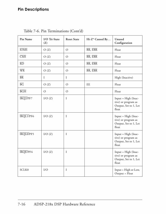
Pin Descriptions
IOMS O (Z) O BR, EBR Float
CMS O (Z) O BR, EBR Float
RD O (Z) O BR, EBR Float
WR O (Z) O BR, EBR Float
BR I I High (Inactive)
BG O (Z) O EE Float
BGH O O Float
IRQ2/PF7 I/O (Z) I Input = High (Inac-tive) or program as Output, Set to 1, Let float
IRQL1/PF6 I/O (Z) I Input = High (Inac-tive) or program as Output, Set to 1, Let float
IRQL0/PF5 I/O (Z) I Input = High (Inac-tive) or program as Output, Set to 1, Let float
IRQE/PF4 I/O (Z) I Input = High (Inac-tive) or program as Output, Set to 1, Let float
SCLK0 I/O I Input = High or Low, Output = Float
Table 7-6. Pin Terminations (Cont’d)
Pin Name I/O Tri-State (Z)
Reset State Hi-Z* Caused By… Unused Configuration
7-16 ADSP-218x DSP Hardware Reference

System Interface
RFS0 I/O I High or Low, Let float if SPORT0 is disabled
DR0 I I High or Low, Let float if SPORT0 is disabled
TFS0 I/O I High or Low, Let float if SPORT0 is disabled
DT0 O O Float
SCLK1 I/O I Input = High or Low, Output = Float
RFS1/IRQ0 I/O I High or Low
DR1/FI I I High or Low, Float if SPORT1 is disabled and the pin is not configured as FI
TFS1/IRQ1 O/I I High or Low
DT1/FO O O Float
EE I I Float
EBR I I Float
EBG O O Float
ERESET I I Float
EMS O O Float
EINT I I Float
Table 7-6. Pin Terminations (Cont’d)
Pin Name I/O Tri-State (Z)
Reset State Hi-Z* Caused By… Unused Configuration
ADSP-218x DSP Hardware Reference 7-17

Pin Descriptions
NOTES* Hi-Z = High impedance1. CLKIN, RESET, and PF3:0/Mode D:Mode A are not included in the table because these pins must
be used.2. All bidirectional pins have tri-stated outputs. When a pin is configured as an output, the output is Hi-Z
(high impedance) when inactive.
Recommendations for Unused Pins
The following is a list of recommendations for unused pins:
• If the CLKOUT pin is not used, turn it OFF, using CLKODIS in the SPORT0 Autobuffer Control register.
• If the Interrupt/Programmable Flag pins are not used, there are two options:
• When these pins are configured as inputs at reset and func-tion as interrupts and input flag pins, pull the pins High (inactive).
• Program the unused pins as outputs. Set them to 1 prior to enabling interrupts and let the pins float.
• If a flag pin is not used, configure it as an output. If for some reason, you cannot configure it as an output, configure it as an input. Use a 100 kΩ pull-up resistor to VDD (or, if this is not possible, use a 100 kΩ pull-down resistor to GND).
ECLK I I Float
ELIN I I Float
ELOUT O O Float
Table 7-6. Pin Terminations (Cont’d)
Pin Name I/O Tri-State (Z)
Reset State Hi-Z* Caused By… Unused Configuration
7-18 ADSP-218x DSP Hardware Reference

System Interface
• If a SPORT is not used completely and if the SPORT pins do not have a second functionality, disable the SPORT and let the pins float.
• If the receiver on a SPORT is the only part being used, use resistors on the other pins. However, if the other pins are outputs, let them float.
Clock SignalsThe ADSP-218x family processors may be operated with a TTL-compati-ble clock signal input to the CLKIN pin or with a crystal connected between the CLKIN and XTAL pins. If an external clock is used, XTAL must be left unconnected. The CLKIN signal may not be halted, changed, or operated below the specified frequency during normal operation.
The ADSP-218x family processors operate with an input clock frequency equal to half the instruction rate; for example, a 16.67 MHz input clock produces a 33 MHz instruction rate (30 ns cycle time). Device timing is relative to the internal clock rate which is indicated by the CLKOUT signal.
Because these processors include an on-chip oscillator circuit, an external crystal can be used. The crystal should be connected between the CLKIN and XTAL pins, with two capacitors connected as shown in Figure 7-1. A parallel-resonant, fundamental frequency, microprocessor-grade crystal should be used. The frequency value selected for the crystal should be half the desired instruction rate.
ADSP-218x DSP Hardware Reference 7-19

Clock Signals
.
Due to the high operating processor core clock speed requirements on some of the ADSP-218x DSPs, it may be advantageous to use a third-overtone crystal rather than a fundamental frequency crystal as an input clock signal in your design. Figure 7-2 shows a sample third over-tone schematic.
CLKIN CLKOUTXTAL
ADSP-218X
Figure 7-1. External Crystal Connections
XTALCLKIN CLKOUT
ADSP-218X
Figure 7-2. Third-Overtone Crystal
7-20 ADSP-218x DSP Hardware Reference

System Interface
In this schematic, a parallel LC circuit is used as a bandpass filter to allow the third harmonic through to the crystal input of the DSP. For example, to operate an ADSP-2189M processor at 75 MHz, an input clock signal with a frequency of 37.5 MHz is required. Using a third overtone crystal circuit would allow you to use a 37.5 MHz third overtone crystal.
The internal phased lock loop (PLL) of the processors generates an inter-nal clock that is four times the instruction rate.
The processors also generate a CLKOUT signal which is synchronized to the processors’ internal cycles and operates at the instruction cycle rate. A phase-locked loop is used to generate CLKOUT and to divide each instruc-tion cycle into a sequence of internal time periods called processor states. The relationship between the phases of CLKIN, CLKOUT, and the processor states is shown in Figure 7-3. The phases of the internal processor clock are dependent upon the period of the external clock.
The CLKOUT output can be disabled on the ADSP-218x processors. This is controlled by the CLKODIS bit in the SPORT0 Autobuffer Control Register.
CLKIN
CLKOUT
INTERNAL
PROCESSOR
STATE
1 2 3 44
PROCESSOR
CYCLE
1 2 3 4
PROCESSOR
CYCLE
Figure 7-3. Clock Signals & Processor States
ADSP-218x DSP Hardware Reference 7-21
Clock Signals
Synchronization DelayEach processor has several asynchronous inputs (interrupt requests, for example), which can be asserted in arbitrary phase to the processor clock. The processor synchronizes such signals before recognizing them. The delay associated with signal recognition is called synchronization delay.
Different asynchronous inputs are recognized at different points in the processor cycle. Any asynchronous input must be valid prior to the recog-nition point to be recognized in a particular cycle. If an input does not meet the setup time on a given cycle, it is recognized either in the current cycle or during the next cycle if it remains valid.
Edge-sensitive interrupt requests are latched internally so that the request signal only has to meet the pulse width requirement. To ensure the recog-nition of any asynchronous input, however, the input must be asserted for at least one full processor cycle plus setup and hold time. Setup and hold times are specified in the data sheet for each individual device.
1/2x Clock ConsiderationsEach processor requires only a 1/2x frequency clock signal. They use what is effectively an on-chip phase-locked loop to generate the higher fre-quency internal clock signals and CLKOUT. Because these clocks are generated based on the rising edge of CLKIN, there is no ambiguity about the phase relationship of two processors sharing the same input clock. Multiple processor synchronization is simplified as a result.
Using a 1/2x frequency input clock with the phase-locked loop to generate the various internal clocks imposes certain restrictions. The CLKIN signal must be valid long enough to achieve phase lock before RESET can be deas-serted. Also, the clock frequency cannot be changed unless the processor is in RESET. Refer to the relevant ADSP-218x processor data sheet for details.
7-22 ADSP-218x DSP Hardware Reference

System Interface
Resetting the ProcessorThe RESET signal halts execution and causes a hardware reset of the proces-sor. The RESET signal must be asserted when the processor is powered up to assure proper initialization. RESET during initial powerup must be held long enough to allow the internal clock to stabilize.
The power-up sequence is defined as the total time required for the crystal oscillator circuit to stabilize after a valid VDD is applied to the processor and for the internal PLL to lock onto the specific crystal frequency. A mini-mum of 2000 CLKIN cycles ensures that the PLL has locked, but it does not include the crystal oscillator start-up time. During the power-up sequence the RESET signal should be held low.
If RESET is activated any time after powerup, the clock continues to run and does not require stabilization time.
! If a clock has not been supplied during RESET, the processor does not know it has been reset and the registers won’t be initialized to the proper values.
At powerup, if RESET is held low (asserted) without any input clock signal, the states of the internal transistors are unknown and uncon-trolled. This condition could lead to processor damage.
Table 7-8 on page 7-25 shows the RESET state of various registers, includ-ing the processors’ on-chip memory-mapped status/control registers. The values of any registers not listed are undefined at reset. The contents of on-chip memory are unchanged after RESET, except as shown in Table 7-8 on page 7-25 for the data-memory-mapped control/status registers. The CLKOUT signal continues to be generated by the processor during RESET, except when disabled.
ADSP-218x DSP Hardware Reference 7-23

Software-Forced Rebooting
The contents of the computation unit (ALU, MAC, Shifter) and data address generator (DAG1, DAG2) registers are undefined following RESET. When RESET is released, the processor’s booting operation takes place, depending on the state of the processor’s MMAP pin. (Program booting is described in Chapter 8, “Memory Interface”.)
In a multiprocessing system with several processors, a synchronous RESET is required.
! When the power supply and clock remain valid, the content of the on-chip memory is not changed by a pulsed RESET line.
Software-Forced RebootingSoftware-forced reboots can be accomplished in different ways. A soft-ware-forced reboot clears the context of the processor and initializes some registers. A context clear clears the processor stacks and restarts execution at address 0x0000. Table 7-7 shows the two different ways the ADSP-218x processor can perform a software reboot.
Table 7-7. Software-Forced Rebooting
Reboot Method Description
Powerup Context Reset
Setting the PUCR bit in the SPORT1 Autobuffer and Powerdown Control register causes a reboot on recovery from powerdown
BDMA Context Reset
Setting the BCR bit in the BDMA Control register before writing to the BDMA Word Count register (BWCOUNT) causes a reboot. Execution starts after the BDMA reboot is completed.
7-24 ADSP-218x DSP Hardware Reference

System Interface
Table 7-8 shows the state of the processor registers after a software-forced reboot. The values of any registers not listed are unchanged by a reboot.
During booting (and rebooting), all interrupts including serial port inter-rupts are masked and autobuffering is disabled. The serial port(s) remain active; one transfer—from internal shift register to data register—can occur for each serial port before there are overrun problems.
The timer runs during a reboot. If a timer interrupt occurs during the reboot, it is masked. Thus, if more than one timer interrupt occurs during the reboot, the processor latches only the first.
Table 7-8. ADSP-218x Processor State After Reset or Software Reboot
Control Field Description Reset Reboot
Bus Exchange register
PX PX register Undefined Undefined
Status registers
IMASK Interrupt service enables 0 0
ASTAT Arithmetic status 0 0
MSTAT Mode status 0 Unchanged
SSTAT Stack status 0x55 0x55
ICNTL Interrupt control Undefined Unchanged
IFC Interrupt force/clear 0 0
ADSP-218x DSP Hardware Reference 7-25

Software-Forced Rebooting
Control registers (memory-mapped)
BPAGE Boot page 0 Unchanged
SPORT1 configure Configuration 1 Unchanged
SPE0 SPORT0 enable 0 Unchanged
SPE1 SPORT1 enable 0 Unchanged
TCOUNT Timer count register Undefined Operates during reboot
TPERIOD Timer period register Undefined Unchanged
TSCALE Timer scale register Undefined Unchanged
PDFORCE Powerdown force 0 Unchanged
PUCR Powerup context reset 0 Unchanged
XTALDIS XTAL pindrive disable during powerdown
0 Unchanged
XTALDELAY Delay startup from power-down (4096 cycles)
0 Unchanged
Serial Port Control registers (memory-mapped, one set per SPORT)
ISCLK Internal serial clock 0 Unchanged
RFSR, TFSR Frame sync required 0 Unchanged
RFSW, TFSW Frame sync width 0 Unchanged
IRFS, ITFS Internal frame sync 0 Unchanged
Table 7-8. ADSP-218x Processor State After Reset or Software Reboot (Cont’d)
Control Field Description Reset Reboot
7-26 ADSP-218x DSP Hardware Reference

System Interface
INVRFS, INVTFS Invert frame sense 0 Unchanged
DTYPE Companding type, format 0 Unchanged
SLEN Serial word length 0 Unchanged
SCLKDIV Serial clock divide Undefined Unchanged
RFSDIV RFS divide Undefined Unchanged
Multichannel word enable bits Undefined Unchanged
MCE Multichannel enable 0 Unchanged
MCL Multichannel length 0 Unchanged
MFD Multichannel frame delay 0 Unchanged
INVTDV Invert transmit data valid 0 Unchanged
RBUF, TBUF Autobuffering enable 0 0
TIREG, RIREG Autobuffer I index Undefined Unchanged
TMREG, RMREG Autobuffer M index Undefined Unchanged
FO (SPORT1 only) Flag Out value Undefined Unchanged
CLKODIS CLKOUT disable 0 Unchanged
BIASRND MAC biased rounding 0 Unchanged
Table 7-8. ADSP-218x Processor State After Reset or Software Reboot (Cont’d)
Control Field Description Reset Reboot
ADSP-218x DSP Hardware Reference 7-27

Software-Forced Rebooting
External Memory Control Registers (non-memory-mapped)
DMOVLAY Data memory overlay select
0 Unchanged
PMOVLAY Program memory overlay select
0 Unchanged
External Memory Control registers (memory-mapped)
DWAIT Data memory overlay wait states
15 (M and N series DSPs only)
0x7 (All other DSPs)
Unchanged
PWAIT Program memory overlay wait states
15 (M and N series DSPs only)
0x7 (All other DSPs)
Unchanged
BMWAIT Byte memory wait states 15 (M and N series DSPs only)
0x7 (All other DSPs)
Unchanged
IOWAIT0-3 I/O memory wait states 15 (M and N series DSPs only)
0x7 (All other DSPs)
Unchanged
CMSSEL Composite memory select 0xB Unchanged
Table 7-8. ADSP-218x Processor State After Reset or Software Reboot (Cont’d)
Control Field Description Reset Reboot
7-28 ADSP-218x DSP Hardware Reference

System Interface
Programmable Flag Data & Control registers (memory-mapped)
PFDATA Programmable flag data Undefined Unchanged
PFTYPE Programmable flag direction
0 Unchanged
DMA Control registers (memory-mapped)
IDMAA IDMA Internal Memory Address
Undefined Unchanged
IDMAD IDMA Destination Memory Type
Undefined Unchanged
BIAD BDMA Internal Memory Address
0 0x201
BEAD BDMA External Memory Address
0 0x601
BTYPE BDMA Transfer Word Type
0 Unchanged
BDIR BDMA Transfer Direction 0 Unchanged
BCR BDMA Context Reset 1 Unchanged
BWCOUNT BDMA Word Count 0x20 01
BMPAGE External Byte Memory Page
0 01
1 These values assume that you have just completed an initial BDMA boot load. For more infor-mation on BDMA register contents during the boot loading process see Table 7-9. These values will vary with a processor reboot (other than initial load), since they depend on the previous values.
Table 7-8. ADSP-218x Processor State After Reset or Software Reboot (Cont’d)
Control Field Description Reset Reboot
ADSP-218x DSP Hardware Reference 7-29

Software-Forced Rebooting
Register Values for BDMA BootingThe state of some registers during reset and rebooting is influenced by the MMAP and BMODE pins in the ADSP-2181 and ADSP-2183 processors and in all other ADSP-218x processors when they are in Full Memory Mode. If these pins are set for a BDMA boot, the values in the BDMA registers change as shown in Table 7-9.
Table 7-9. BDMA Registers before and after Initial Boot Loading
Register Description1 Value Before Boot Value After Boot
BIAD BDMA Internal Memory Address. Set for internal address 0.
0 0x20
BEAD BDMA External Memory Address. Set for external address 0.
0 0x60
BTYPE BDMA Transfer Word Type. Set for 24-bit program memory words.
0 0
BDIR BDMA Transfer Direction. Set to transfer data from byte memory.
0 0
BMPAGE BDMA Page Selection. Set to byte memory page 0.
0 0
BWCOUNT BDMA Word Count. Set to trans-fer 32 words.
0x20 0
BMWAIT BDMA Port Wait States. Set to 7 waits per transfer.
0xF (M and N series DSPs only)
0x7 (All other DSPs)
0xF (M and N series DSPs only)
0x7 (All other DSPs)
7-30 ADSP-218x DSP Hardware Reference

System Interface
External InterruptsADSP-218x family processors have a number of prioritized, individually maskable, external interrupts, which can be either level- or edge-triggered. These interrupt request pins are named IRQ0, IRQ1, and IRQ2. The IRQ0 and IRQ1 pins are only available as the (optional) alternate configuration of SPORT1. The configuration of SPORT1 as either a serial port or as inter-rupts (and flags) is determined by bit 10 of the processor’s system control register.
The ADSP-218x processors also have two dedicated level-triggered inter-rupt request pins and one dedicated edge-triggered interrupt request pin; these are IRQL0, IRQL1, and IRQE, respectively.
Internal interrupts, including serial port, timer, and DMA, are discussed in other chapters. Additional information about interrupt masking, set up, and operation can be found in Chapter 3, Program Sequencer.
BCR BDMA Context Reset2 1 1
BMOVLAY3 BDMA Overlay value 0 0
1 Assumes MMAP=0 and BMODE=0 for a BDMA boot (applies to ADSP-2181 and ADSP-2183 processors) or MODEA=0 and MODEB=0 for all other ADSP-218x processors).
2 Set to 1 to:(a) Hold off instruction execution during BDMA transfer(b) Start execution at address PM(0x0000) after BDMA transfer(c) Leave a BDMA interrupt pending This sequence of events occurs if BCR is set before BWCOUNT is written, or after the initial boot.
3 Applies only to the following processors: ADSP-2187L/N, ADSP-2188M/N, and ADSP-2189M/N.
Table 7-9. BDMA Registers before and after Initial Boot Loading (Cont’d)
Register Description1 Value Before Boot Value After Boot
ADSP-218x DSP Hardware Reference 7-31

External Interrupts
Interrupt SensitivityIndividual external interrupts can be configured in the ICNTL register as either level-sensitive or edge-sensitive.
Level-sensitive interrupts operate by asserting the interrupt request line (IRQx) until the request is recognized by the processor. Once recognized, the request must be deasserted before unmasking the interrupt so that the DSP does not continually respond to the interrupt.
In contrast, edge-triggered interrupt requests are latched when any high-to-low transition occurs on the interrupt line. The processor latches the interrupt so that the request line may be held at any level for an arbi-trarily long period between interrupts. This latch is automatically cleared when the interrupt is serviced. Edge-triggered interrupts require less exter-nal hardware than level-sensitive requests since there is never a need to hold or negate the request. With level-sensitive interrupts, however, many interrupting devices can share a single request input; this allows easy sys-tem expansion.
An interrupt request will be serviced if it is not masked (in the IMASK regis-ter) and a higher priority request is not pending. Valid requests initiate an interrupt servicing sequence that vectors the processor to the appropriate interrupt vector address. See Chapter 3, “Program Sequencer” for the ADSP-218x processor interrupt vector addresses. There is a synchroniza-tion delay associated with both external interrupt request lines and internal interrupts.
If an interrupt occurs during a waitstated external memory access or dur-ing the extra cycles required to execute an instruction that accesses external memory more than once, it is not recognized between the cycles, only before or after. Edge-sensitive interrupts are latched, but not ser-viced, during bus grant (BG) unless the Go mode is enabled.
7-32 ADSP-218x DSP Hardware Reference
System Interface
In order to service an interrupt, the processor must be running and exe-cuting instructions. The IDLE instruction can be used to effectively halt processor operations while waiting for an interrupt.
Edge-sensitive and level-sensitive interrupt requests are serviced similarly. Edge-sensitive interrupts may remain active (low) indefinitely, while level-sensitive interrupts must be deasserted before the RTI instruction is executed; otherwise, the same interrupt immediately recurs.
Care must be taken with the serial port (SPORT1) that can be configured for alternate functions (IRQ0 and IRQ1). If the RFS1 or TFS1 input is held low when SPORT1 is configured as the serial port and then is reconfig-ured as IRQ0 and IRQ1, an interrupt request can be generated. This interrupt request can be cleared with the use of the IFC register.
Flag PinsAll ADSP-218x processors provide flag pins. The alternate configuration of SPORT1 includes a Flag In (FI) pin and a Flag Out (FO) pin. The con-figuration of SPORT1 as either a serial port or as flags and interrupts is selected by bit 10 of the processor’s System Control register.
The FI pin can be used to control program branching, using the IF FLAG_IN and IF NOT FLAG_IN conditions of the JUMP and CALL instructions. These conditions are evaluated based on the last state of the FI pin; FLAG_IN is true if FI was last sampled as a 1 and false if last sampled as a 0. FO can be used as a general purpose external signal. The state of FO is also available as a read-only bit of the SPORT1 control register.
ADSP-218x DSP Hardware Reference 7-33
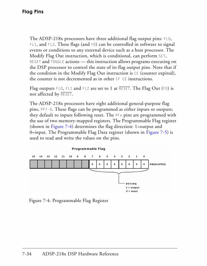
Flag Pins
The ADSP-218x processors have three additional flag output pins: FL0, FL1, and FL2. These flags (and FO) can be controlled in software to signal events or conditions to any external device such as a host processor. The Modify Flag Out instruction, which is conditional, can perform SET, RESET and TOGGLE actions — this instruction allows programs executing on the DSP processor to control the state of its flag output pins. Note that if the condition in the Modify Flag Out instruction is CE (counter expired), the counter is not decremented as in other IF CE instructions.
Flag outputs FL0, FL1 and FL2 are set to 1 at RESET. The Flag Out (F0) is not affected by RESET.
The ADSP-218x processors have eight additional general-purpose flag pins, PF7–0. These flags can be programmed as either inputs or outputs; they default to inputs following reset. The PFx pins are programmed with the use of two memory-mapped registers. The Programmable Flag register (shown in Figure 7-4) determines the flag direction: 1=output and 0=input. The Programmable Flag Data register (shown in Figure 7-5) is used to read and write the values on the pins.
Program mable Flag
PFTYP E
1 = output
0 = input
DM(0x3FE6)
15 14 13 12 11 10 9 8 7 6 5 4 3 2 1 0
0 0 0 00 0 0 0
Figure 7-4. Programmable Flag Register
7-34 ADSP-218x DSP Hardware Reference

System Interface
Data being read from a pin configured as an input is synchronized to the processor’s clock. Pins configured as outputs drive the appropriate output value. When the PFDATA register is read, any pins configured as outputs will read back the value being driven out.
Powerup IssuesThe ADSP-218x dual-voltage M and N series processors have special issues related to powerup. These issues include the powerup sequence and the dual-voltage power supplies. This section discusses both these issues. it also gives information about reset generators, which provide a reliable active reset once the power supplies and internal clock circuits have stabilized.
Powerup SequenceThe following recommendations should be observed when powering dual-voltage DSP’s. Ideally the two supplies, VDDEXT and VDDINT, should be powered up together. If they cannot be powered up together, the internal (core) supply should be powered up first. Powering up the core supply first reduces the risk of latchup events.
PFDATA
Programmable Flag Data
DM(0x3FE5)
15 14 13 12 11 10 9 8 7 6 5 4 3 2 1 0
Figure 7-5. Programmable Flag Data Register
ADSP-218x DSP Hardware Reference 7-35

Powerup Issues
A network of protection diodes, as shown in Figure 7-6, isolates the inter-nal supplies and provides ESD protection for the IO pins. When applying power separately to the VDDINT or VDDEXT pins, care should be taken to limit the maximum supply current and duration that would be conducted through the isolation diodes if the unpowered pins are at ground potential.
If an external master clock is used, it should not be driving the CLKIN pin when the DSP is unpowered. The clock must be driven immediately after powerup; otherwise, internal gates stay in an undefined (hot) state and can draw excess current. After powerup, there should be sufficient time for the internal PLL to stabilize (2000 clock cycles) before the reset is released.
ADSP-218X M-SERIES DSP
INTERNAL LOGIC
VDDEXT VDDINT
(2.5V)(2.5-3.3V)
IO PIN
OUTPUT
INPUT
Figure 7-6. Protection Diodes and IO Pin ESD Protection
7-36 ADSP-218x DSP Hardware Reference

System Interface
In addition, time should be allowed for the oscillator to start up and reach full amplitude. This may take 100 ms, depending upon choice of crystal, operating frequency, loop gain, and capacitor ratios. Startup time may be more significant than the 2000 clock cycles needed for the PLL to stabilize.
Power Supplies
The following lists the power supplies that ADSP-218x processors can use:
• ADSP-218x L series processors use a single 3.3 V power supply
• ADSP-218x M series processors can use either a single 2.5 V power supply or a 2.5 V internal power supply and a 3.3 V power supply for I/O
• ADSP-218x N series processors can use either a single 1.8 V power supply or a 1.8 V internal power supply and either a 2.5 V or a 3.3 V power supply for I/O
ADSP-218x DSP Hardware Reference 7-37

Powerup Issues
Dual Supply Example
To provide 2.5 V and 3.3 V power supplies for the ADSP-218x M series processors, it is suggested that a dual regulator, powered from a common source, be used. Analog Devices does not currently have a 2.5 V/3.3 V dual-output regulator; however, it does have several suitable single output regulators.
We suggest the low drop-out regulators, ADP3330ART-2.5 and ADP3330ART-3.3, which are identical parts but with different (fixed) output voltages. These regulators are available in SOT-23-6, a very small, six lead surface mount package, and will provide 2.5 V @ 70 mA and 3.3 V @ 90 mA from a 5 V supply at ambient temperatures up to 85°C. This power supply is suitable for the dual-voltage M series of DSPs—up to their maximum operating temperature and clock frequencies.
These regulators also accept an active low, shut down signal, which is use-ful for many low power applications that require power saving schemes. An open collector output error signal is available to permit appropriate action in the event that the input voltage has fallen too low to permit effi-cient regulation.
7-38 ADSP-218x DSP Hardware Reference

System Interface
Figure 7-6 provides a suggested schematic using these regulators.
2
3
6
1
5
4
10 F
10 F
SHTDWN
ERR
SD
NR
GND
2
3
6
1
5
4
10 F
REGERR
20K
(70mA MAX)
(107mA MAX)
ERR
SD
VO U T
NR
GND
µ
µ
µ
10 Fµ
ADP3330ART-3.3
ADP3330AR T-2.5
+2.5VD DIN T
+3.3V DD EXTVIN VIN VO U T
VIN
Figure 7-7. Suggested Dual Power Supply for ADSP-218x M Series DSPs
ADSP-218x DSP Hardware Reference 7-39

Powerup Issues
Reset GeneratorsIt is important that a DSP (or programmable device) have a reliable active RESET that is released once the power supplies and internal clock circuits have stabilized. The RESET signal should not only offer a suitable delay, but it should also have a clean monotonic edge. Analog Devices has a range of microprocessor supervisory ICs with different features. Features include one or more of the following:
• Powerup reset
• Optional manual reset input
• Power low monitor
• Back-up battery switching
Part number series for Analog Devices’ supervisory circuits are as follows:
• ADM69x
• ADM70x
• ADM80x
• ADM1232
• ADM181x
• ADM869x
7-40 ADSP-218x DSP Hardware Reference

System Interface
A simple powerup reset circuit is shown below, using the ADM809-RART reset generator. The ADM809 provides an active low RESET signal when-ever the supply voltage is below 2.63 V. At powerup, a 240 ms active reset delay is generated to give the power supplies and oscillators time to stabilize.
V
RESET
GND
ADM 809-RART
VDDEXT
RESET
GND
+3.3VDDEXT
10µF
CC
ADSP-218X-M
VDDINT
+2.5VDDINT
Figure 7-8. Simple Reset Generator for M Series DSPs
ADSP-218x DSP Hardware Reference 7-41

Powerup Issues
Another part, the ADM706TAR, provides poweron RESET and optional manual RESET. It allows designers to create a more complete supervisory circuit that monitors the supply voltage. Monitoring the supply voltage allows the system to initiate an orderly shutdown in the event of power failure. The ADM706TAR also allows designers to create a watchdog timer that monitors for software failure. This part is available in an eight lead SOIC package. Figure 7-9 shows a typical application circuit using the ADM706TAR.
RESET
IRQ2
IRQL1
FL0
GNDRESET
Vt=+1.25V
VSENSE
VDDEXT
PFI
MR
WDI
PFO
WDO
GND
4
1
6
5
8
3
ADM706TARVCC
2RST
7
100nF
10µF
100nF
VDDEXT +3.3V
ADSP-218x-M
Figure 7-9. Reset Generator and Power Supply Monitor
7-42 ADSP-218x DSP Hardware Reference

System Interface
PowerdownThe ADSP-218x processors provide a powerdown feature that allows the processor to enter a very low power dormant state through hardware or software control. In this CMOS standby state, power consumption is less than 1 mW (approximate). (Refer to the processor data sheet for exact power consumption specifications.)
The powerdown feature is useful for applications where power conserva-tion is necessary, for example in battery-powered operation. Features of powerdown include:
• Internal clocks are disabled
• Processor registers and memory contents are maintained
• Ability to recover from powerdown in less than 100-400 CLKIN cycles (the number of cycles depends on the processor used in your system design; see the appropriate data sheet for information)
• Ability to disable internal oscillator when using crystal
• No need to shut down clock for lowest power when using external oscillator
• Interrupt support for executing “housekeeping” code before enter-ing powerdown and after recovering from powerdown
• User selectable powerup context
ADSP-218x DSP Hardware Reference 7-43

Powerdown
Even though the processor is put into the powerdown mode, the lowest level of power consumption still might not be achieved if certain guide-lines are not followed. Lowest possible power consumption requires no additional current flow through processor output pins and no switching activity on active input pins. Therefore, a careful analysis of pin loading in your circuit is required. The following sections detail the proper power-down procedure as well as provide guidelines for clock and output pin connections required for optimum low-power performance.
Powerdown ControlYou can control several parameters of powerdown operation through con-trol bits in the SPORT1 Autobuffer/Powerdown Control Register.
This control register is memory-mapped at location 0x3FEF and is shown in Figure 7-10.
SPORT1 Autobuffer / Powerdown Control Register
15 14 13 12 11 10 9 8 7 6 5 4 3 2 1 0
XTALDISXTAL Pin Drive Disable During Powerdown
1=disabled, 0=enabled(XTAL pin should be disabled when
no external crystal is connected)
XTALDELAY
1=delay, 0=no delay(Use delay to allow internal phase locked
loop or external oscillator to stabilize)
PDFORCEPowerdown Force
1=force processor to vector to powerdown interrupt
PUCRPowerup Context Reset
1=soft reset (clear context)*, 0=resume execution
DM(0x3FEF)
Delay Startup From Powerdown 4096 Cycles
Figure 7-10. SPORT1 Autobuffer/Powerdown Control Register
7-44 ADSP-218x DSP Hardware Reference
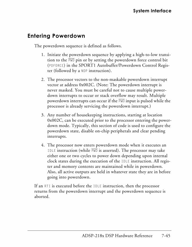
System Interface
Entering Powerdown The powerdown sequence is defined as follows.
1. Initiate the powerdown sequence by applying a high-to-low transi-tion to the PWD pin or by setting the powerdown force control bit (PDFORCE) in the SPORT1 Autobuffer/Powerdown Control Regis-ter (followed by a NOP instruction).
2. The processor vectors to the non-maskable powerdown interrupt vector at address 0x002C. (Note: The powerdown interrupt is never masked. You must be careful not to cause multiple power-down interrupts to occur or stack overflow may result. Multiple powerdown interrupts can occur if the PWD input is pulsed while the processor is already servicing the powerdown interrupt.)
3. Any number of housekeeping instructions, starting at location 0x002C, can be executed prior to the processor entering the power-down mode. Typically, this section of code is used to configure the powerdown state, disable on-chip peripherals and clear pending interrupts.
4. The processor now enters powerdown mode when it executes an IDLE instruction (while PWD is asserted). The processor may take either one or two cycles to power down depending upon internal clock states during the execution of the IDLE instruction. All regis-ter and memory contents are maintained while in powerdown. Also, all active outputs are held in whatever state they are in before going into powerdown.
If an RTI is executed before the IDLE instruction, then the processor returns from the powerdown interrupt and the powerdown sequence is aborted.
ADSP-218x DSP Hardware Reference 7-45

Powerdown
While the processor is in the powerdown mode, the processor is in CMOS standby. This allows the lowest level of power consumption where most input pins are ignored. Active inputs need to be held at CMOS levels to achieve lowest power. For more information, see “Processor Operation During Powerdown” on page 7-51.
Exiting PowerdownThe powerdown mode can be exited with the use of the PWD pin or with RESET. There are also several user-selectable modes for start-up from pow-erdown which specify a start-up delay as well as specify the program flow after start-up. This allows the program to resume from where it left off before powerdown or for the program context to be cleared.
Ending Powerdown with the Powerdown Pin
Applying a low-to-high transition to the PWD pin will take the processor out of powerdown mode. You have the option of selecting the amount of time the processor takes to come out of the powerdown mode with the “delay start-up from powerdown” control bit (XTALDELAY), bit 14 in the Powerdown Control register. If this bit is cleared to 0, no additional delay is introduced over the quick start-up (between 100 and 400 cycles, as specified in the relevant ADSP-218x data sheet). If this bit is set to 1, a delay of 4096 cycles is introduced. The delay feature is used depending upon the state of an external clock oscillator at the time of powerup or if the internal clock is disabled. For more information, see the sections, “Systems Using an External TTL/CMOS Clock” on page 7-48 and “Systems Using a Crystal and the Internal Oscillator” on page 7-49.
You can also program one of two options directing the processor how to resume operation. The context for exiting powerdown is set by bit 12 (PUCR, powerup context reset) of the Powerdown Control register.
7-46 ADSP-218x DSP Hardware Reference

System Interface
If the PUCR control bit is cleared to 0, the processor will continue to exe-cute instructions following the IDLE instruction. For example, a high-to-low transition is applied to the pin, which causes the processor to vector to the powerdown interrupt routine. In this routine, a few house-keeping tasks are performed and the IDLE instruction is executed. The processor powers down. Some time later a low-to-high transition is applied to the pin, causing the processor to exit powerdown mode. Since the PUCR bit is 0, the processor resumes executing instructions in the pow-erdown interrupt routine, starting at the instruction following the IDLE instruction. When an RTI instruction is encountered, control then passes back to the main routine.
If the PUCR bit is set to 1 for a clear context, the processor resumes opera-tion from powerdown by clearing the PC, STATUS, LOOP and CNTR stacks. The IMASK and ASTAT registers are set to 0 and the SSTAT goes to 0x55. The processor will start executing instructions from address 0x0000.
Ending Powerdown with the RESET Pin
If RESET is asserted while the processor is in the powerdown mode, the processor is reset and instructions are executed from address 0x0000. A boot is performed if the MMAP pin is set to 0 for the ADSP-2181 and ADSP-2183 processors or the MODE A and MODE B pins are set to 0 for all other ADSP-218x processors.
If the RESET pin is used to exit powerdown, then it must be held low for the appropriate number of cycles. If the clock is stopped at powerup or operating at a different frequency at powerup than it was before power-down, RESET must be held long enough for the oscillator to stabilize plus an additional 1000 CLKIN cycles for the phase-locked loop to lock. The time required for the oscillator to stabilize depends upon the type of crys-tal used and capacitance of the external crystal circuit. Typically 2000 CLKIN cycles is adequate for clock stabilization time.
ADSP-218x DSP Hardware Reference 7-47

Powerdown
If the clock was not stopped at powerup and is at a stable frequency at powerup (same as before powerdown), only 5 cycles of RESET are required.
When ending powerdown with RESET, the XTALDELAY (delay start-up from powerdown) control bit is ignored.
Startup Time after PowerdownThe time required to exit the powerdown state depends on whether an internal or external oscillator is used, and the method used to exit powerdown.
Systems Using an External TTL/CMOS Clock
When the processor is in powerdown, the external clock signal is ignored if the XTALDIS bit (XTAL pin disable) of the Powerdown Control register is set to 1. It is therefore not necessary to stop the external clock since no power is wasted while the external clock is running. If the external clock is to be stopped anyway, it must be kept running for (at least) one additional cycle after the IDLE instruction is executed.
The XTALDIS bit should always be set before entering powerdown. This specifies that the XTAL pin is not to be driven by the processor. During powerdown, there is no need to drive the XTAL pin when an external oscil-lator is used. Disabling the XTAL pin drive during powerdown lets the input clock run without wasting power.
After the processor is taken out of the powerdown mode by either the PWD pin or RESET, it will begin executing instructions after a maximum start-up time of between 100 and 400 CLKIN cycles (see the relevant ADSP-218x data sheet for the correct specification) as long as the clock oscillator is sta-ble and at the same frequency as before powerdown.
7-48 ADSP-218x DSP Hardware Reference

System Interface
If the external clock is unstable when the processor exits powerdown, then the XTALDELAY control bit can be used. This allows time for the external clock to stabilize by inserting an additional 4096-cycle delay before the processor starts to execute instructions. The start-up delay can only be used when the processor is taken out of powerdown mode with the PWD pin.
If the processor is taken out of powerdown by RESET and the clock is stable and at the same frequency as before powerdown, RESET needs to be held for only 5 cycles.
Systems Using a Crystal and the Internal Oscillator
A trade-off can be made so that a fast start-up is possible, but power is consumed by leaving the oscillator running during powerdown. If a fast start-up is desired, then you must clear bits 14 (XTALDELAY) and 15 (XTALDIS) of the Powerdown Control Register to 0 before entering powerdown. This selects no additional delay after start-up from power-down and drives the external crystal during powerdown. In this configuration, the oscillator will continue to operate and the processor will start executing instructions in less than 100 or 400 cycles after the low to high signal transition at the pin. (The number of cycles depends upon the processor used in your system design; please see the appropriate data sheet for specific timing information.) The XTAL pin will also be driven and the powerdown power consumption will be higher than the 1 mW specification. The following code example shows the powerdown interrupt routine.
/* Sample Powerdown Code *//* Located at interrupt vector address 0x002C */ pwd_int: ax0 = 0x0000; /* enable crystal, no delay */ dm(0x3FEF) = ax0; idle; rti;
ADSP-218x DSP Hardware Reference 7-49

Powerdown
If the lowest possible power consumption is required, then you must set the XTALDELAY and XTALDIS bits to 1 before entering powerdown. This set-ting does the following:
• Selects the additional 4096 cycle delay to allow the oscillator to start and the phase locked loop to lock after start-up.
• Disables the drive to the XTAL pin during powerdown.
The following code example shows the powerdown interrupt routine.
/* Sample Powerdown Code *//* Located at interrupt vector address 0x002C */ pwd_int: ax0 = 0xC000; /* disable crystal, delay */ dm(0x3FEF) = ax0; idle; rti;
Depending on the particular situation and external system conditions, the powerdown modes shown above could be set conditionally. If you want to powerdown for a long time you may want to set the mode for lowest power consumption. If you want to powerdown for a short time, lowest power consumption may not be that important.
If the RESET pin is used to exit powerdown and the clock has been stopped, then RESET must be held low for 1000 CLKIN cycles plus the time required for the phase locked loop to lock and the crystal oscillator to stabilize (typ-ically 2000 CLKIN cycles.) If the clock is running during powerdown, a RESET signal of only 5 cycles is required.
7-50 ADSP-218x DSP Hardware Reference

System Interface
Processor Operation During PowerdownSome processor circuitry may still be active during powerdown mode. Also, some output pins remain active. A good understanding of these states will allow you to determine the best low-power configuration for your system. By keeping output loading and input switching to a mini-mum the lowest possible power consumption can be achieved.
Interrupts and Flags
Interrupts are latched and can be serviced if the processor exits power-down without a context reset (PUCR=1). Any activity on the interrupt or flag input pins during powerdown will increase the power consumption. There should also be no resistive load on the flag output pins (as with any active output pin) if lowest power is desired.
SPORTs
The circuitry of the serial ports is not directly affected by powerdown. The SPORTs are indirectly affected if an internally generated SCLK or frame sync is required. SPORT circuitry continues to operate during powerdown.
It is possible to clock data into or out of the serial ports during power-down. You must supply an external serial clock to support operation during powerdown. No interrupts or autobuffer operations will be ser-viced during powerdown. Instead, the SPORT interrupts are latched and can be serviced if the processor exits powerdown without resetting the processor. Data clocked into the processor will remain in the receive (RX) registers. Autobuffer transfers will occur after the device exits powerdown if the processor is not powered up with RESET. Note that any SPORT activity will increase the power consumption above the 1 mW specification.
ADSP-218x DSP Hardware Reference 7-51

Powerdown
If an external serial clock and an external frame sync signal are supplied, data can be clocked into the RX register or out of the TX register during powerdown. Since the TX register can not be updated while the processor is in powerdown, the same value is repeatedly clocked out the serial port. Also, data in the RX register is continually overwritten since the RX register can not be read by the processor during powerdown.
If an external serial clock is used with an internal frame sync, frame sync signals continue to be generated during powerdown since they are derived from the serial clock. Data bits continue to be received with the RX register being overwritten. Since data is only transmitted when the TX register is written, data bits are only transferred out of the processor if the processor is put in powerdown during a serial port transfer. While the processor is being put into powerdown, the serial port transfer in progress is allowed to complete. Since an internally generated transmit frame sync is used, no subsequent frame syncs are generated while in powerdown.
If internal serial clock is used, there is no SPORT activity during power-down; the serial clock stops.
Lowest power dissipation is achieved when active SPORT pins are not changing during powerdown and are held at CMOS levels.
7-52 ADSP-218x DSP Hardware Reference

System Interface
IDMA Port During Powerdown
The IDMA port can receive data during powerdown, but it can not respond with an acknowledge (IACK) signal or increment the IDMA inter-nal address. If you are using a short read or short write and are in the middle of an IDMA transfer, you can complete a single read or write while the processor is in powerdown. If you are using the long read or long write method and are in the middle of an IDMA transfer, your host must be able to handle a “timeout” condition, as the DSP will not return an acknowledge to the transfer in process.
Note that IDMA activity while the DSP is in powerdown uses power and should be avoided to conserve power. For more information on lowest power use, see For more information, see “Conditions for Lowest Power Consumption” on page 7-54.
BDMA Port During Powerdown
Do not powerdown the ADSP-218x processor during a BDMA transfer. If you do, the DSP will not be able to recover correctly from powerdown and the contents of memory accessed by the processor’s BDMA port will be corrupted.
If you need to go into powerdown mode, either:
• Verify that the BWCOUNT register contains a zero. If a BDMA transfer is in process, poll the BWCOUNT register to determine when the trans-fer is done.
or
• Abort any BDMA transfer in progress by writing 1 to the BWCOUNT register and go into powerdown when the BWCOUNT register contains a zero. (Note that the BDMA transfer is not properly completed in this case.)
ADSP-218x DSP Hardware Reference 7-53

Powerdown
Conditions for Lowest Power ConsumptionThe state of all processor pins during powerdown is shown in Table 7-10.
To assure the lowest power consumption, all active input pins should be held at a CMOS level (to ground level, if possible). All active output pins should be free of resistive load since load current will increase power dissi-pation. You must perform a careful analysis of each input and output pin in order to insure lowest power dissipation.
Some inputs are active but ignored. The state of these inputs does not matter as long as they are at a CMOS level.
Table 7-10. Pin States During Powerdown
Pin Direction State During Powerdown
RESET I Active
PWD I Active
IRQ2 I Active, latched but not serviced
IRQE I Active, latched but not serviced
IRQL0 I Active, latched but not serviced
IRQL1 I Active, latched but not serviced
MMAP I Active
BR I Active, no response until after powerdown
BG O Driven HIGH unless bus is granted
CLKIN I Input buffer inactive, but XTAL oscillator is active unless XTALDIS bit is set
CLKOUT O Driven HIGH
7-54 ADSP-218x DSP Hardware Reference

System Interface
XTAL O Driven HIGH if XTALDIS set, inversion of CLKIN otherwise
PWDACK O Driven HIGH
PMS O Driven HIGH, high impedance if bus granted
DMS O Driven HIGH, high impedance if bus granted
BMS O Driven HIGH, high impedance if bus granted
IOMS O Driven HIGH, high impedance if bus granted
CMS O Driven HIGH, high impedance if bus granted
RD O Driven HIGH, high impedance if bus granted
WR O Driven HIGH, high impedance if bus granted
ADDR<13:0> O High impedance
DATA<23:0> I Inactive
DATA<23:0> O High impedance
SCLK0 I Active
SCLK0 O Driven to static level if internal, high impedance otherwise
TFS0 I Active if SPORT 0 is enabled
TFS0 O Driven if configured internal or in multichannel mode and SPORT 0 enabled, high impedance otherwise
RFS0 I Active if SPORT 0 is enabled
Table 7-10. Pin States During Powerdown (Cont’d)
Pin Direction State During Powerdown
ADSP-218x DSP Hardware Reference 7-55

Powerdown
RFS0 O Driven if configured internal and SPORT 0 enabled, high impedance otherwise
DR0 I Active if SPORT 0 is enabled
DT0 O Driven if serial port operating. Output may be static or changing depending upon serial clock, high impedance otherwise
SCLK1 I Active
SCLK1 O Driven to a static level if internal, high imped-ance otherwise
TFS1/IRQ1 I Active if SPORT 1 is enabled or configured alter-nate (IRQ1)
TFS1 O Driven if SPORT 1 is enabled and configured for internal transmit framing, high impedance other-wise
RFS1/IRQ0 I Active if SPORT 1 is enabled or configured alter-nate (IRQ0)
RFS1 O Driven if SPORT 1 is enabled and config-ured for internal receive framing, high impedance otherwise
DR1/FI I Active if SPORT 1 is enabled or configured alter-nate (FI)
DT1/FO O Driven if serial port operating. Output may be static or changing depending upon serial clock. Driven if SPORT 1 is enabled or configured alternate (FO)
FL<2:0> O Driven to previous value
Table 7-10. Pin States During Powerdown (Cont’d)
Pin Direction State During Powerdown
7-56 ADSP-218x DSP Hardware Reference

System Interface
PWDACK PinThe powerdown acknowledge pin (PWDACK) is an output that indicates when the processor is powered down. This pin is driven high by the pro-cessor when it has powered down and is driven low when the processor has completed its powerup sequence. A low level on the PWDACK pin also indi-cates that there is a valid CLKOUT signal and that instruction execution has begun. Figure 7-11 shows an example of timing for the powerdown and restart sequence.
The processor is executing code when the PWD pin is brought low. The pro-cessor vectors to the powerdown interrupt vector and an IDLE instruction is executed causing the processor to go into powerdown. The CLKOUT and PWDACK signals are driven high by the processor. At this point, the input clock pin is ignored. If the processor is put into the powerdown mode via the powerdown force bit in the powerdown control register, the result is the same as described above.
PF<7:0> I/O Active
BMODE I Active
IRD I Active, if IS asserted
IWR I Active, if IS asserted
IS I Active
IAL I Active, if IS asserted
IAD I/O Active, if an operation in progress
IACK O Active
Table 7-10. Pin States During Powerdown (Cont’d)
Pin Direction State During Powerdown
ADSP-218x DSP Hardware Reference 7-57
Powerdown
The input clock is started and the PWD pin is brought high. After the neces-sary start-up cycles the processor brings the PWDACK output low, begins driving the CLKOUT pin with a clock signal and begins to fetch the instruc-tion after the IDLE instruction. The processor then resumes normal operation.
When powerdown is terminated with the RESET pin or if a start-up delay is selected, a low level on the PWDACK pin only indicates the start of oscilla-tions on the CLKOUT pin. It will not necessarily indicate the start of instruction execution.
The state of PWDACK and also the CLKOUT signal is undefined during the first 100 cycles of initial reset.
RUN
CLKIN
CLKOUT
PWDACK
PWD
PWRDWNPENDING
POWEREDDOWN
RUNSTART CLK
EXECUTEIDLE
FINISH IDLE
NOP WHILE FETCHING INSTRUCTION FOLLOWING IDLE
Figure 7-11. Powerdown Timing Examples
7-58 ADSP-218x DSP Hardware Reference
System Interface
Using Powerdown as a Non-Maskable InterruptThe powerdown interrupt is never masked. It is possible to use this inter-rupt for other purposes if desired. The processor will not go into powerdown until an IDLE instruction is executed. If an RTI is executed before the IDLE instruction, then the processor returns from the power-down interrupt and the powerdown sequence is aborted.
It is possible to place a series of instructions at the powerdown interrupt vector location 0x002C. This routine should end with an RTI instruction and not contain an IDLE instruction if the interrupt is to be used for pur-poses other than powerdown.
Bus Request/GrantThis section describes the bus request and grant feature of the ADSP-218x processors.
An ADSP-218x processors can relinquish control of data and address buses to an external device. The external device requests the bus by assert-ing (low) the bus request signal, BR. The BR signal is an asynchronous input. If the ADSP-218x processor is not performing an external access, it responds to the active BR input in the following processor cycle by:
1. Tristating the data and address buses and the xMS, RD, WR output drivers,
2. Asserting the bus grant (BG) signal, and
3. Halting program execution (unless Go mode is enabled).
If Go mode is enabled, the ADSP-218x processor continues to execute instructions from its internal memory. It will not halt program execution until it encounters an instruction that requires an external access. (An external access may be either a memory device access or a memory overlay access, BDMA access, or I/O space access.)
ADSP-218x DSP Hardware Reference 7-59

Bus Request/Grant
If Go mode is not enabled, the ADSP-218x processor always halts before granting the bus. The processor’s internal state is not affected by granting the bus, and the serial ports remain active during a bus grant, whether or not the processor core halts.
If the ADSP-218x processor is performing an external access when the BR signal is asserted, it will not grant the buses until the cycle after the access completes. The sequence of events is illustrated in Figure 7-12. The entire instruction does not need to be completed when the bus is granted. If a single instruction requires two external accesses, the bus will be granted between the two accesses. The second access is performed after BR is removed.
CLKOUT
BR
BG
BR
BG
If no memory access is in progress, BG is asserted in the cycle after BR is recognized:
PMS
DMSBMS
PMS
DMS
BMS
If a memory access is in progress, BG is asserted in the cycle after the access is completed:
Figure 7-12. Bus Request (With or Without External Access)
7-60 ADSP-218x DSP Hardware Reference

System Interface
When the BR input is released, the ADSP-218x processor releases the BG signal, reenables the output drivers and continues program execution from the point where it stopped. BG is always deasserted in the same cycle that the removal of BR is recognized. Refer to the data sheet for exact timing relationships.
The bus request feature operates at all times, including when the processor is booting and when RESET is active. During RESET, BG is asserted in the same cycle that BR is recognized. During booting, the bus is granted after completion of loading of the current byte (including any wait states). Using bus request during booting is one way to bring the booting opera-tion under control of a host computer.
The ADSP-218x processors also have a Bus Grant Hung (BGH) output, which lets them operate in a multiprocessor system with a minimum num-ber of wasted cycles. The BGH pin asserts when the ADSP-218x processor is ready to execute an instruction but is stopped because the external bus is granted to another device. The other device can release the bus by deas-serting bus request. Once the bus is released, the ADSP-218x processor deasserts BG and BGH and executes the external access.
ADSP-218x DSP Hardware Reference 7-61
Target System Hardware
Target System HardwareThis section provides target system hardware recommendations to assist you in preventing problems with an EZ-ICE emulation system.
Target Board Connector for EZ-ICE ProbeThe ADSP-218x processor has on-chip emulation support and an ICE-port, which is comprised of a special set of pins that interface to the EZ-ICE. By using only a 14-pin connection from the target system to the EZ-ICE, this interface allows for in-circuit emulation without replacing the target system processor. This 14-pin connection is a standard, 0.100-inch on-center, pin-strip header. Target systems must have a 14-pin connector to accept the EZ-ICE’s in-circuit probe, a 14-pin female plug.
Figure 7-13 shows the EZ-ICE connector (a standard pin strip header). You must add this connector to your target board design if you intend to use the EZ-ICE.
! Be sure to allow enough room in your system to fit the EZ-ICE probe onto the 14-pin connector.
7-62 ADSP-218x DSP Hardware Reference

System Interface
The 14-pin, 2-row pin strip header is keyed at the Pin 7 location—you must remove Pin 7 from the header. The pins must be 0.025 inches square and at least 0.20 inches in length. Pin spacing should be 0.1 x 0.1 inches. The pin strip header must have at least a 0.15 inch clearance on all sides to accept the EZ-ICE probe plug.
! Pin strip headers are available from vendors such as 3M, McKenzie (Framatome Connectors International), and Samtec, Inc.
The ICE-Port interface consists of the following ADSP-218x processor pins: EBR, EINT, EE, EBG, ECLK, ERESET, ELIN, EMS, and ELOUT. These ADSP-218x processor pins must be connected only to the EZ-ICE con-nector in the target system. These pins have no function, other than during emulation, and do not require pull-up or pull-down resistors. All of the emulator signals become active once the Emulation Enable (EE) sig-nal is driven high.
X
1 2
3 4
5 6
7 8
9 10
11 12
13 14
GND
KEY (NO P IN)
RESET
BR
BG
TOP VIEW
EBG
EBR
ELOUT
EE
EINT
ELIN
ECLK
EMS
ERESET
Figure 7-13. EZ-ICE Connector
ADSP-218x DSP Hardware Reference 7-63

Target System Hardware
! The traces for these signals between the ADSP-218x processor and the connector must be kept as short as possible — no longer than 3 inches.
The following pins are also used by the EZ-ICE: BR, BG, RESET, and GND.
The EZ-ICE uses the EE signal to take control of the ADSP-218x proces-sor in the target system. This causes the processor to use its ERESET, EBR, and EBG pins instead of the RESET, BR, and BG pins. The BG output is tri-stated.
! These signals do not need to be jumper-isolated in your system.
The EZ-ICE connects to your target system via a ribbon cable and a 14-pin female plug. The female plug is plugged onto the 14-pin connector (a pin strip header) on the target board.
Using Mode Pins with RESET and ERESET Signals
Issuing the CHIP RESET command during emulation causes the DSP to perform a full chip reset. The state of the Mode pins are latched upon the rising edge of the RESET signal; this holds true when the DSP is reset in a running system or when a CHIP RESET command is issued when in emula-tion mode.
! Therefore, when using the EZ-ICE with a 100-pin ADSP-218x pro-cessor, it is vital that the Mode pins are set correctly prior to issuing a CHIP RESET command from the emulator user interface.
If you are using a passive method of maintaining mode information (as discussed in “Active or Passive Mode Pin Configuration” on page 7-13), then it does not matter that the mode information is latched by an emula-tor reset. However, if you are using the RESET pin as a method of actively setting the value of the Mode pins, then you need to take into consider-ation the effects of an emulator reset.
7-64 ADSP-218x DSP Hardware Reference

System Interface
One method of ensuring that the values located on the Mode pins are those desired is to construct a circuit like the one shown in Figure 7-14. The circuit shown in this figure forces the value located on the Mode A pin to a logic high, regardless of whether it is latched via the RESET or ERESET pin. (To configure the Mode pin to a logic low, you could use a two-input AND gate with the ERESET and RESET signals connected as inputs and the output of the AND gate connected to the Mode pin. In this example, the Mode pin would be driven to a logic low when either the RESET or the ERESET signals go active low.)
Bus Request SignalThe Bus Request signal (BR) should be pulled high with a 10 kΩ resistor if itis not being used in your system design. Failure to pull BR high may result inthe inability of EZ-ICE to fully initialize when connected to a target.Since the microcontroller uses the Bus Request signal to communicatewith the DSP, it is critical that you do not leave BR floating, even if you arenot using it in your target.
E R E S E T
P R O G R A M M A B L E I/O
M O D E A /P F O
R E S E T
1 k
A D S P -21 8X
Figure 7-14. EZ-ICE Circuit for ADSP218x Mode Pins
ADSP-218x DSP Hardware Reference 7-65

Target System Hardware
! When not using the emulator, the BR pin must be pulled high. If it is not pulled high, either a hold-off condition could occur, which can halt the DSP from booting either via BDMA or IDMA, or pro-gram execution could halt indefinitely. Typical behavior for this problem would be no activity on the BMS signal, or the IACK signal staying inactive (high) indefinitely.
Memory Select SignalsAll memory select signals should be pulled high for EZ-ICE emulator compatibility.
You must connect a pull-up resistor (10 kΩ) on the memory select signals (RD, WR, PMS, DMS, BMS, CMS, and IOMS) if they are used in your target system. (For example, you would use these signals when accessing external mem-ory or memory-mapped peripheral devices.) Pull-up resistors are needed since there are no internal pull-ups to guarantee the memory select signal’s state during prolonged tri-stated conditions, which result from typical EZ-ICE debugging sessions. Because the EZ-ICE uses the DSP’s bus to communicate with Program Memory (PM), Data Memory (DM), Boot Memory (BM), Input Output Memory (IOM), and Emulator Memory Space, pull-up resistors must be used.
Decoupling Capacitors0.1 µF decoupling capacitors should be placed (as close to the DSP as pos-sible) on all VDD pins connected to the same digital ground.
During clock and data transitions, when all signal pins switch simulta-neously, decoupling capacitors provide a localized source DC voltage and current for optimal operation of the DSP. Decoupling capacitors also ensures that there is a low-impedance power source present in power planes and circuit traces. They effectively remove high frequencies from the signal trace while not affecting lower frequencies.
7-66 ADSP-218x DSP Hardware Reference

System Interface
All other digital integrated circuit chips in your system should be decou-pled to manufacturers recommendations.
Also, a 100 µF bypass capacitor can be placed at the rails of the power supply coming into the target board to filter unwanted RF noise from the power supply cable.
RESET SignalDue to the high operating speeds of RC circuits, using them to delay the deassertion of the RESET signal at powerup is not recommended for ADSP-218x processor systems. During powerup, RESET must be held low for a minimum of 2000 DSP CLKIN cycles to ensure proper phase-lock loop of the internal processor clock. Achieving proper phase-lock loop ensures that the CLKOUT signal phase-locks with the CLKIN signal.
A Schmitt Trigger (or some type of hysteresis circuitry) should be used on the reset line to minimize “ringing” on the RESET signal or to allow for mechanical debouncing of a push button or switch. A clean RESET signal that is free from ringing or glitches guarantees proper DSP powerup and initialization. Without a Schmitt Trigger, the RESET signal may oscillate or ring before settling to a valid inactive (high) level. Ringing on the RESET signal may cause the DSP to lock up, since the RESET signal may fall below the VIH minimum voltage specification. When the signal falls below this minimum, a faulty reset that does not meet the 2000 CLKIN cycle mini-mum DSP specification can occur.
PCB Board Whenever possible, target systems should consist of a multilayered PCB board with a separate power and ground plane stacked in the middle layers of the board. Wirewrapped boards are not generally recommended as they are more susceptible to external noise and parasitic capacitance.
ADSP-218x DSP Hardware Reference 7-67

Target System Hardware
EZ-ICE Powerup ProcedureThe ADSP-218x EZ-ICE communicates with a host PC over an RS232 serial cable. Connect the ADSP-218x EZ-ICE board to the selected COM port of the PC (COM1 or COM2) using the attached RS232 serial cable of the emulator.
Below is the recommended powerup sequence when using the emulator to debug your target system:
1. Power up the ADSP-218x EZ-ICE by using the supplied power adapter. Also, power up your target system.
2. Using the provided ground cable, attach one end of the ground cable to the emulator probe at reference location TP1. Attach the other end of the ground cable to a proper ground on your target system.
3. Attach the emulator probe to your target board’s 14-pin emulator header.
4. Invoke the emulator software.
! Reverse this procedure for removing the ADSP-218x EZ-Ice from your target system.
Other ConsiderationsWhen designing a target system, keep the following in mind:
• EZ-ICE emulation introduces an up to 15 pF load on the RESET and BR signals. See the ADSP-218x Family Hardware Installation Guide for more details.
• EZ-ICE emulation introduces an up to 15 pF load on the BG signal. In some modes the EZ-ICE drives the BG signal. See the ADSP-218x Family Hardware Installation Guide for more details.
7-68 ADSP-218x DSP Hardware Reference

System Interface
• EZ-ICE emulation ignores RESET and BR when single-stepping.
• EZ-ICE emulation ignores RESET and BR when in Emulator Space (DSP Halted).
• EZ-ICE emulation ignores the state of the target BR in certain modes. As a result, the target system may take control of the DSP’s external memory bus only if bus grant (BG) is asserted by the EZ-ICE board’s DSP.
• EZ-ICE emulation introduces a 500 µs latency between transitions to User Space and some signal responses. This latency occurs when you start (or resume) running your DSP program. The latency is the time between resumption of code execution and the EZ-ICE board allowing the DSP to respond to RESET and BR.
Recommended ReadingThe text High-Speed Digital Design: A Handbook of Black Magic is recom-mended for further reading. This book is a technical reference that covers the problems encountered in state-of-the-art, high-frequency digital cir-cuit design, and is an excellent source of information and practical ideas. Topics covered in the book include:
• High-Speed Properties of Logic Gates
• Measurement Techniques
• Transmission Lines
• Ground Planes & Layer Stacking
• Terminations
• Vias
• Power Systems
ADSP-218x DSP Hardware Reference 7-69

Target System Hardware
• Connectors
• Ribbon Cables
• Clock Distribution
• Clock Oscillators
Reference: Johnson & Graham, High-Speed Digital Design: A Handbook of Black Magic, Prentice Hall, Inc., ISBN 0-13-395724-1.
7-70 ADSP-218x DSP Hardware Reference

8 MEMORY INTERFACEFigure 8-0.
Table 8-0.
Listing 8-0.
OverviewThe ADSP-218x family of processors has a modified Harvard architecture in which data memory stores data and program memory stores both instructions and data. A program instruction or opcode can be fetched from internal memory and executed. In the same clock cycle, two data ele-ments can be accessed from internal memory: one from Data Memory and the other from Program Memory.
Program Memory and Data MemoryEach ADSP-218x family processor contains on-chip RAM, which allows a portion of the Program Memory space and a portion of the Data memory space to reside on-chip. External Program Memory and external Data Memory can also be used in a system design. 16 K words total of external Program Memory (24-bits) and 16 K words total of external Data Mem-ory (16-bits) can be addressed as 8 K overlay memory segments.
ADSP-218x DSP Hardware Reference 8-1

Overview
Byte Memory SpaceEach processor has a 4 M addressable byte-wide memory space (Byte Memory space). This space can be used for the following:
• Loading on-chip program memory with code from an external EPROM at reset
• Bulk code or data storage during runtime
• Software overlays when a program’s code size exceeds the amount of on-chip memory on the processor
I/O Memory SpaceThe ADSP-218x processors support I/O Memory space. This space is a 16-bit, 2048 location that allows for the memory mapping of external peripherals or other processors to the ADSP-218x processor. External memory select signals are associated with each of these external memory spaces.
Memory BusesIn each ADSP-218x family processor, memory is connected to the internal functional units by four on-chip buses: the Data Memory Address (DMA) bus, Data Memory Data (DMD) bus, Program Memory Address (PMA) bus and Program Memory Data (PMD) bus. The internal PMA bus and DMA bus are multiplexed into a single address bus that is extended off-chip. Likewise, the internal PMD bus and DMD bus are multiplexed into a single external data bus. The sixteen MSBs of the external data bus are used as the DMD bus: external bus lines D23-8 are used for DMD15-0.
8-2 ADSP-218x DSP Hardware Reference

Memory Interface
External Memory SpacesThere are four separate external memory spaces: Data Memory, Program Memory, Byte Memory, and I/O Memory. To provide external access to these memory spaces, the ADSP-218x processors extend the 14-bit inter-nal address bus and 24-bit data bus off-chip and provide the PMS, DMS, BMS, and IOMS select lines. The PMS, DMS, BMS, and IOMS signals indicate which memory space is being accessed.
Because the Program Memory and Data Memory buses are multiplexed off-chip, if more than one external transfer must be made in the same instruction, an overhead cycle will be required. An overhead cycle is not required if just one off-chip access (with no wait states) occurs in any instruction.
All external memories may have automatic wait state generation associated with them. The number of wait states—each equal to one instruction cycle—is programmable.
Composite Memory SelectThe Composite Memory Select (and its CMS select line) lets a single off-chip memory be accessed as multiple memory spaces. The Composite Memory Select register lets you define which memory spaces are selected by the CMS signal. By using this register, you can assign the CMS signal to become active on any combination of Program Memory, Data Memory, Byte Memory, or I/O Memory external memory accesses.
External Overlay MemoryExternal Program Memory and external Data Memory can be addressed as 8 K overlay memory segments (pages). These overlay segments are mapped to addresses 0x2000-0x3fff for Program Memory overlay regions and 0x0000-0x1fff for Data Memory overlay regions.
ADSP-218x DSP Hardware Reference 8-3

Overview
Internal Direct Memory Access PortThe Internal Direct Memory Access (IDMA) port is a 16-bit slave port that supports booting from an external host processor. This port also allows the host runtime access to all of the internal memory contents (both internal Program Memory and Data Memory) of the DSP—except for the memory-mapped control registers, which reside at the uppermost 32 locations of internal Data Memory. The DMA feature of this port lets you define the number of memory locations the DSP transfers to or from internal memory in the background while continuing foreground processing.
Memory ModesThe IDMA port is a separate port on the ADSP-2181 and ADSP-2183 processors and a configured port on all other ADSP-218x processors. For all of the ADSP-218x family processors, except for the ADSP-2181 and ADSP-2183, the external address and data pins are multiplexed with the IDMA address/data bus and control signals. The functionality of these multiplexed pins is determined at reset by external Mode pins. The value of these Mode pins determine whether the 100-pin ADSP-218x processors have access to the full 14-bit address bus and 24-bit data bus (Full Mem-ory Mode) or if the processor has IDMA functionality (Host Memory Mode) with a single address bit (A0) and a 16-bit data bus (D[23:8]).
The pin multiplexing design enables processors to use a smaller number of pins, which results in a smaller package size. This reduced size helps save board “real estate” in board size-critical applications. On the other hand, this reduced size requires a more complex design in order to use both the external address and data busses simultaneously with IDMA port functionality.
8-4 ADSP-218x DSP Hardware Reference

Memory Interface
Memory InterfacesIn the modified Harvard architecture used by ADSP-218x processors, Pro-gram Memory stores both instructions and 24-bit or 16-bit data values; Data Memory stores 16-bit data values only. The amount of on-chip memory differs for each processor. Table 8-1 identifies the amount of on-chip memory contained in each processor.
Figures 8-1 through 8-6 show the on-chip Program Memory and Data Memory configurations and their address mappings for each of the ADSP-218x family processors.
Table 8-1. ADSP-218x Processor Base On-Chip Memory
Processor Program Memory Data Memory
ADSP-2181 16 K by 24-bit words 16 K by 16-bit words
ADSP-2183 16 K by 24-bit words 16 K by 16-bit words
ADSP-2184, ADSP-2184L and ADSP-2184N
4 K by 24-bit words 4 K by 16-bit words
ADSP-2185, ADSP-2185L, ADSP-2185M, and ADSP-2185N
16 K by 24-bit words 16 K by 16-bit words
ADSP-2186, ADSP-2186L, ADSP-2186M, and ADSP-2186N
8 K by 24-bit words 8 K by 16-bit words
ADSP-2187L and ADSP-2187N 32 K by 24-bit words 32 K by 16-bit words
ADSP-2188M and ADSP-2188N 48 K by 24-bit words 56 K by 16-bit words
ADSP-2189M and ADSP-2189N 32 K by 24-bit words 48 K by 16-bit words
ADSP-218x DSP Hardware Reference 8-5

Memory Interfaces
Program Memory
PM Overlay 0(Internal P M )
PM Overlay 1,2(External PM )
0x3FFF
0x2000
Internal PM
0x1FFF
0x0000
0x3FE0
0x3FDF
Data M em ory
DM Overlay 0(Internal DM )
DM Overlay 1,2(External DM)
Internal DM
32-M em ory-M appedControl Registers
Figure 8-1. ADSP-2181, ADSP-2183, and ADSP-2185 Memory Archi-tecture (MMAP=0 for ADSP-2181 and ADSP-2183, and Mode B=0 for ADSP-2185)
Program Memory
PM Overlay 1,2(External PM)
0x3FFF
0x2000
Internal PM 0x0FFF
0x0000
0x3FE00x3FDF
Data Memory
DM Overlay 1,2(External DM)
Internal DM
32-Memory-MappedControl Registers
4064 Reserved Words
Internal PM Reserved
Internal DM Reserved
Reserved
0x3000
0x2FFF
0x1000
Figure 8-2. ADSP-2184 Memory Architecture (Mode B=0)
8-6 ADSP-218x DSP Hardware Reference

Memory Interface
Program Memory
0x3FFF
0x2000
0x0000
0x3FE00x3FDF
Data Memory
DM Overlay 1,2(External DM)
Internal DM
32-Memory-MappedControl Registers
Internal DM Reserved
0x1FFF
PM Overlay 1,2(External PM)
Internal PM
Internal PM Reserved
Figure 8-3. ADSP-2186 Memory Architecture (Mode B=0)
Program Memory
0x3FFF
0x2000
0x0000
0x3FE00x3FDF
Data Memory
DM Overlay 0,4,5(Internal DM)
DM Overlay 1,2(External DM
Internal DM
32-Memory-MappedControl Registers
0x1FFF
PM Overlay 0,4,5(Internal PM)
PM Overlay 1,2(External PM)
Internal PM
Figure 8-4. ADSP-2187 Memory Architecture (Mode B=0)
ADSP-218x DSP Hardware Reference 8-7

Memory Interfaces
Program Memory
0x3FFF
0x2000
0x0000
0x3FE00x3FDF
Data Memory
DM Overlay 0,4,5,6,7,8(Internal DM)
DM Overlay 1,2(External DM)
Internal DM
32-Memory-MappedControl Registers
0x1FFF
PM Overlay 0,4,5,6,7(Internal PM)
PM Overlay 1,2(External PM)
Internal PM
Figure 8-5. ADSP-2188 Memory Architecture (Mode B=0)
Program Memory
0x3FFF
0x2000
0x0000
0x3FE00x3FDF
Data Memory
DM Overlay 0,4,5,6,7(Internal DM)
DM Overlay 1,2(External DM)
Internal DM
32-Memory-MappedControl Registers
0x1FFF
PM Overlay 0,4,5(Internal PM)
PM Overlay 1,2(External PM)
Internal PM
Figure 8-6. ADSP-2189 Memory Architecture (Mode B=0)
8-8 ADSP-218x DSP Hardware Reference
Memory Interface
These memory maps show how the internal memory is configured for each of the ADSP-218x family processors. Since the ADSP-2184 and ADSP-2186 processors have less than 16 K words of Program Memory and Data Memory, some of their internal memory locations are reserved and should not be used in the Linker Description File (LDF) or accessed at runtime in the executable program. Please note that all external mem-ory locations map to Program Memory and Data Memory overlay pages 1 and 2.
Program Memory InterfaceThe ADSP-218x family Program Memory is 24-bits wide. Up to two accesses to internal Program Memory can be completed per instruction cycle. Instruction read accesses are done on the first half of the clock cycle, and data reads and writes are done on the second half of the clock cycle.
The Program Memory Address bus is 14 bits in length. This length allows the ADSP-218x processors to directly access 16 K of internal Program Memory. For processors with more than 16 K internal Program Memory, the additional memory regions are accessed or selected as 8 K Program Memory overlay segments, using a Program Memory Overlay register (PMOVLAY). This register acts as a program memory page select.
All of the ADSP-218x family processors can also access up to 16 K of external Program Memory. External Program Memory is also selected by using the Program Memory Overlay register. Only one overlay region can be active at a time; this restriction applies to both internal and external overlay regions.
ADSP-218x DSP Hardware Reference 8-9

Memory Interfaces
The PWAIT field of the System Control register sets the number of wait states for each access to external Program Memory overlays. The value of the PWAIT bit field of the System Control register defaults to fifteen after reset for all ADSP-218x M and N series processors. Bit 15 of the System Control register for these ADSP-218x M and N series processors defaults to 1, which assigns twice the value of the PWAIT bit field plus one (2N+1) wait states. The PWAIT bit field defaults to seven after reset for all other ADSP-218x processors.
For all ADSP-218x processors, Program Memory Overlay regions 1 and 2 correspond to external Program Memory overlay regions, each 8 K in length. All other overlay regions are internal overlays, except for Overlay region 3, which is reserved. External Program Memory overlays are selected by using the Program Memory Overlay register (PMOVLAY). Only one Program Memory overlay region can be active at a time; this restric-tion applies to both internal and external Program Memory overlay regions.
! Internal Program Memory overlay regions do not apply to the ADSP-2184 and ADSP-2186 processors.
When accessing external Program Memory overlay pages, the PMOVLAY reg-ister controls or determines the value of the address pin A13. When the PMOVLAY register equals 1, the value of A13 is zero. When the PMOVLAY reg-ister equals two, the value of address pin A13 is 1. Table 8-2 explains the operational behavior of the PMOVLAY register and address pin A13 when using external Program Memory overlay pages.
8-10 ADSP-218x DSP Hardware Reference

Memory Interface
The on-chip Program Memory and internal and external Program Mem-ory overlay regions can hold both instructions and data intermixed in any combination. By assigning the memory architecture description in the Linker Description File, a programmer can specify absolute address place-ment for any code or data module, including code for the interrupt vector table and reset vector. The reset vector is located at Program Memory address 0x0000. In conjunction with the Linker Description File, the ADSP-218x processor linker determines where to place relocatable code and data segments.
All of the Program Memory overlay regions map from address location PM(0x2000) to PM(0x3FFF). The value of the Program Memory Overlay register (PMOVLAY), determines which overlay region is currently being accessed and whether an internal or an external PM overlay region is being accessed by the DSP core.
Table 8-2. PMOVLAY and Program Memory Overlay Addressing
PMOVLAY Memory A13 A12:0
0,4,5,6,7 Internal 8 K Region N/A N/A
1 External 8 K Overlay 1 0 13 LSBs of address between 0x2000 and 0x3FFF
2 External 8 K Overlay 2 1 13 LSBs of address between 0x2000 and 0x3FFF
ADSP-218x DSP Hardware Reference 8-11
Memory Interfaces
! ADSP-218x processors’ program sequencer operates independently from the PMOVLAY register. The program sequencer only operates on the absolute address of the current instruction it is executing. For Program Memory, the overlay regions map to the address range 0x2000 – 0x3fff. Special care must be taken by the programmer to ensure that the proper target address and overlay are accessed when making jumps or calls in the program.
Also, the DAG registers operate independently of the PMOVLAY reg-ister. Again, special care must be taken to ensure the proper target Program Memory region is being accessed when performing register indirect jump or call instructions or when performing serial port autobuffering to Program Memory overlay regions.
Data Memory InterfaceThe Data Memory of the ADSP-218x family processors is 16-bits wide. Similar to the internal Program Memory of these processors, up to two accesses to internal Data Memory can be completed per instruction cycle. Memory read accesses are done on the first half of the clock cycle and memory writes are done on the second half of the clock cycle.
The Data Memory Address bus is 14 bits in length; the ADSP-218x pro-cessor can directly access 16 K of internal Data Memory. For processors with more than 16 K of internal Data Memory, the additional memory regions are accessed or selected as 8 K Data Memory overlay segments using a Data Memory Overlay (DMOVLAY) register. This register acts as a Data Memory page select.
8-12 ADSP-218x DSP Hardware Reference

Memory Interface
For all ADSP-218x processors, Data Memory Overlay regions 1 and 2 cor-respond to external Data Memory overlay regions, each 8 K in length. All other overlay regions are internal overlays, except for Overlay 3, which is reserved. External Data Memory overlays are selected by using the Data Memory Overlay register (DMOVLAY). Only one Data Memory overlay region can be active at a time; this restriction applies to both internal and external Data Memory overlay regions.
! Internal Data Memory overlay regions do not apply to the ADSP-2184 and ADSP-2186 processors.
The DWAIT field of the Wait State Control register sets the number of wait states for each access to external Data Memory overlays. The value of the DWAIT bit field of the System Control register defaults to seven after reset for all ADSP-218x M and N series processors, but the total number of wait states is fifteen for these processors. Bit 15 of the Wait State Control register for these ADSP-218x M and N series processors defaults to 1, which assigns twice the value of the DWAIT bit field plus one (2N+1) wait states. The DWAIT bit field defaults to seven after reset for all other ADSP-218x processors.
The on-chip Data Memory and internal and external Data Memory over-lay regions can be used to store data. By assigning the memory architecture description in your Linker Description File, you can specify absolute address placement for any data segment. In conjunction with your Linker Description File, the ADSP-218x linker determines where to place relocatable data segments.
ADSP-218x DSP Hardware Reference 8-13

Memory Interfaces
When accessing external Data Memory overlay pages, the DMOVLAY register controls or determines the value of the address pin A13. When the DMOVLAY register equals 1, the value of A13 is 0. When the DMOVLAY register equals 2, the value of address pin A13 is 1. Table 8-3 explains the operational behav-ior of the DMOVLAY register and address pin A13 when using external Data Memory overlay pages.
All of the Data Memory overlay regions map from address location DM(0x0000) to DM(0x1FFF). The value of the Data Memory Overlay regis-ter (DMOVLAY) determines which overlay region is currently being accessed and whether an internal or an external DM overlay region is being accessed by the DSP core.
! Since the DMOVLAY register works independently from the program sequencer and DAGs, special care must be taken by the programmer to ensure that the proper target memory location is accessed. For example, the programmer should take care when switching between Data Memory Overlay regions while serial port autobuffering is active. On a positive note, this switching could allow the program-mer to configure the serial port autobuffering mechanism to operate in “ping-pong” fashion when switching between overlay memory regions.
Table 8-3. DMOVLAY and Data Memory Overlay Addressing
DMOVLAY Memory A13 A12:0
0,4,5,6,7,8 Internal 8 K Region NA NA
1 External 8 K Overlay 1 0 13 LSBs of address between 0x0000 and 0x1FFF
2 External 8 K Overlay 2 1 13 LSBs of address between 0x0000 and 0x1FFF
8-14 ADSP-218x DSP Hardware Reference

Memory Interface
Listing 8-1 provides example instructions that demonstrate how to use the DMOVLAY register.
Listing 8-1. DMOVLAY Register Example
DMOVLAY=DM(0x1234); /* type 3 instruction, DMOVLAY is loaded with the contents of addressDM(0x1234) */
DMOVLAY=2; /* type 7 instruction, DMOVLAY is loadedwith the value 2 */
DMOVLAY=AX0; /* DMOVLAY is loaded from AX0 register */AX0=DMOVLAY; /* AX0 is loaded from DMOVLAY register */
Byte Memory InterfaceThe ADSP-218x processor’s Byte Memory space is 8 bits wide and can address up to 4M bytes of program code or data. The ADSP-218x proces-sor can boot through this interface, as well as performing read and write accesses to an 8-bit memory device via the BDMA port during runtime. The external signal BMS is active during Byte Memory accesses.
Each read or write to Byte Memory consists of data (which is driven on data bus lines D[15:8]) and address information (driven on address lines A[13:0], concatenated with data lines D[23:16]). This gives the BDMA port a total of 22 bits of addressing, which allows you to access up to 4M byte of ROM or RAM. This memory can be read from or written to in four different formats: 24-bit code, 16-bit data, 8-bit data MSB aligned, or 8-bit data LSB aligned. For 8-bit MSB aligned accesses, the LSBs are zero padded during byte memory reads. For 8-bit LSB aligned accesses, the MSBs are zero padded during byte memory reads.
Wait states for Byte Memory accesses are programmable via the BMWAIT bit field of the Programmable Flag and Composite Memory Select Control register. For the ADSP-218x M and N series processors, the default setting for BMWAIT is fifteen after reset. For all other ADSP-218x processors, the default setting is seven after reset.
ADSP-218x DSP Hardware Reference 8-15

Memory Interfaces
For more information on the ADSP-218x processor’s Byte Memory and BDMA port, please refer to the “BDMA Port” section in Chapter 9, “DMA Ports”.
I/O Memory SpaceThe ADSP-218x family processors have a dedicated 16-bit wide I/O Memory space consisting of 2048 locations. This dedicated memory space allows you to memory map peripherals using this space rather than using external Program Memory and/or external Data Memory addressing and resources to interface with external devices.
There are four programmable wait state regions that are associated with I/O Memory space. The Wait State Control register contains the IOWAIT0:3 bit fields that control the four I/O Memory wait state regions, consisting of 512 locations each.
For the ADSP-218x M and N series processors, the default setting for IOWAIT is 15 after reset. For all other ADSP-218x processors, the default setting is 7 after reset. Figure 8-7 shows the Wait State Control register and the IOWAIT0:3 fields that control I/O Memory wait state regions for the ADSP-218x M and N series processors. Figure 8-8 shows the same information for all other ADSP-218x processors.
IOWAIT0IOWAIT1IOWAIT2IOWAIT3DWAIT
DM(0X3FFE)
Wait State Mode Select0 = normal mode (PWAIT, DWAIT, IOWAIT0-3 = N wait states, ranging from 0 to 7)1= 2N+1 mode (PW AIT, DWAIT, IOWAIT0-3 = 2N+1 wait states, ranging from 0 to 15)
W ait State Control
15 14 13 12 11 10 9 8 7 6 5 4 3 2 1 0
1 1 1 11 1 1 11 1 1 1 1 1 1 1
(ADSP-218x M and N Series Processors)
Figure 8-7. Wait State Control Register (ADSP-218x M and N Series)
8-16 ADSP-218x DSP Hardware Reference

Memory Interface
The Wait State Control register is divided into the following fields:
• IOWAIT0—This 3-bit field sets the number of wait states (0-7) for accesses to I/O Memory addresses 0x000-0x1ff.
• IOWAIT1—This 3-bit field sets the number of wait states (0-7) for accesses to I/O Memory addresses 0x200-0x3ff.
• IOWAIT2—This 3-bit field sets the number of wait states (0-7) for accesses to I/O Memory addresses 0x300-0x4ff.
• IOWAIT3—This 3-bit field sets the number of wait states (0-7) for accesses to I/O Memory addresses 0x400-0x5ff.
! For the ADSP-218x M and N series processors, bit 15 of the Wait State Control register operates as a Wait State Mode Select bit. When set, this bit configures the external I/O memory accesses to a “2N+1” wait state mode. This 2N+1 wait state mode also applies for external Program Memory and Data Memory accesses via the DWAIT field of the Wait State Control register and the PWAIT field of the System Control register.
IOWAIT0IOWAIT1IOWAIT2IOWAIT3DWAIT
DM(0x3FFE)
Bit 15 is unusedand should beset to 0.
Wait State Control
15 14 13 12 11 10 9 8 7 6 5 4 3 2 1 0
1 1 1 11 1 1 10 1 1 1 1 1 1 1
(All ADSP-218x Processors except ADSP-218x M and N Series)
Figure 8-8. Wait State Control Register (All ADSP-218x Processors except M and N Series)
ADSP-218x DSP Hardware Reference 8-17

Memory Interfaces
The following assembly instructions are examples of how I/O memory locations can be accessed during run time:
ax0 = 0x1234; /* Write a value to ax0 register */IO(0x1ff) = ax0; /* I/O Memory write */
ay1 = IO(ASIC_Host); /* Read data value from I/O Memory MappedASIC */
" Since I/O Memory space is a separate, dedicated memory space, the address mapping for I/O Memory space is not included as informa-tion in your Linker Description File. The only method of assigning (and accessing) I/O Memory in your system is during runtime in your assembly code. (I/O Memory space is not directly supported by the C Runtime Environment.)
Because of this restriction, in order to guarantee proper system per-formance, the programmer and system designer must take special care to ensure that the correct address mapping is performed both in hardware and in software.
Composite Memory SelectThe ADSP-218x family processors have a programmable memory select signal, Composite Memory Select (CMS). This signal lets you generate a memory select for devices mapped to more than one memory space, with the same timing as the other individual memory select signals (PMS, DMS, BMS, and IOMS).
8-18 ADSP-218x DSP Hardware Reference

Memory Interface
Based on the value of the CMSSEL bit field (bits 11:8) in the Composite Select Control register (see Figure 8-9), the ADSP-218x processor asserts CMS when the corresponding memory select signal(s), PMS, DMS, BMS, and IOMS, are asserted. The CMS signal can be enabled to become active for any of these signals individually. By default after reset, the CMSSEL field is ini-tialized to enable the CMS signal to become active for any PMS, DMS, or IOMS memory access. (BMS is disabled.)
Figure 8-10 and Figure 8-11 in the next sections provide two examples for using the CMS signal in system designs.
1 = Enable CM S
CMSSEL
0 = Disable CM S
DM(0x3FE6)
15 14 13 12 11 10 9 8 7 6 5 4 3 2 1 0
DMBMIOM PM
Composite Select Control
1 0 1 1
Figure 8-9. CMSSEL Selection for CMS Signal
ADSP-218x DSP Hardware Reference 8-19

Memory Interfaces
CMS Signal as Chip Select for 32 K x 8-Bit SRAMs
Figure 8-10 provides an example of using the CMS signal as a chip select for three 32 K x 8-bit SRAMs with no glue logic. The purpose of this chip select is to implement two pairs of 8 K external overlay regions: two for Program Memory and two for Data Memory.
D[0:7] D[0 :7] D[0 :7]D[16:23]
D[8:15]
D[0:7]
A[0:13]
A[0:13] A[0:13]A[0:13]
A[14] A[14]A[14]
CSCM S
PM S
32K X 8 32K X 832K X 8
ADSP-218X
OE
WE
RD
WR
CS
OE
WE
CS
OE
WE
Figure 8-10. Example Using CMS Signal as a Chip Select
8-20 ADSP-218x DSP Hardware Reference

Memory Interface
In this example, the CMS signal is configured to trigger for both Program Memory and Data Memory accesses (when the PMS or DMS signals are active). The PMS signal is used as the upper order address line (A[14]) to the SRAMs. When the DSP performs Program Memory accesses, the PMS signal becomes active (low), causing the A14 address line of the SRAMs to be driven low. When the DSP performs Data Memory accesses, the PMS signal becomes inactive, causing the A14 address line of the SRAMs to be driven high.
The main advantage of this implementation is that only three 32 K x 8-bit SRAMs are required for this configuration. Normally, five 16 K x 8-bit SRAMs are required to implement two pairs of 8 K overlay regions for Program Memory and Data Memory. This implementation helps to save on board “real estate” where board space is limited.
BMS Disable
For the following ADSP-218x models, there is a disable BMS control bit (bit 3 of the System Control register) that allows the processor core to enable or disable the BMS signal during Byte Memory accesses:
• ADSP-2184, ADSP-2184L and ADSP-2184N
• ADSP-2185L, ADSP-2185M, and ADSP-2185N
• ADSP-2186, ADSP-2186L, ADSP-2186M, and ADSP-2186N
• ADSP-2187L and ADSP-2187N
• ADSP-2188M and ADSP-2188N
• ADSP-2189M and ADSP-2189N
When BMS is disabled, it can be used with the CMS signal to allow the map-ping of multiple memory devices to the Byte Memory space. Figure 8-11 provides an example of this use of the BMS and CMS signals.
ADSP-218x DSP Hardware Reference 8-21

Memory Interfaces
In this example, the DSP is booted from an EPROM. By default after reset, the BMS signal is enabled for Byte Memory accesses. After the DSP has been booted and initialized during runtime, the system program can disable the BMS signal and also enable the CMS signal to trigger during BMS accesses. This process allows the CMS signal to chip select the FLASH or SRAM memory during runtime while leaving the BMS signal disabled. Leaving the BMS signal disabled prevents any contention between the two devices.
D[16:23]
D[0:7] D[0:7]/
/
8
8
A[0:13]
A[0:22] A[0:22]
CS CS
CM S
BM S
EPROM FLASH or SRAM
ADSP-218X
OERD
WR
OE
WE
D[8:15]
Figure 8-11. Example Using CMS Signal to Chip Select FLASH or SRAM Memory
8-22 ADSP-218x DSP Hardware Reference

Memory Interface
Memory Interface ModesAll ADSP-218x family processors, except for the ADSP-2181 and ADSP-2183, are available in a 100-lead LQFP package. The ADSP-218x
processors in 100-lead LQFP packages can be used in one of two modes; Full Memory Mode or Host Memory Mode. Full Memory Mode allows complete operation of the external 24-bit data and 14-bit address busses with full external overlay memory and I/O capability. Host Memory Mode allows complete IDMA functionality with limited external address-ing capabilities. The operating mode is determined by the state of the Mode C pin only during the rising edge of the RESET signal. The operating mode cannot be changed while the processor is running.
Full Memory ModeIn Full Memory Mode, the ADSP-218x processors in 100-lead LQFP packages have complete use of the external address and data busses. In this mode, the processors behave in exactly the same manner as the ADSP-2181 and ADSP-2183 processor with the IDMA port removed.
The processors have a 24-bit external data bus, a 14-bit address bus and 5 memory select signals. Byte memory is accessed for data by using the mid-dle eight bits of the data bus. The upper eight bits of the data bus combined with the 14 address pins provide a 22 bit address for Byte Mem-ory space. All of these features behave exactly the same as they do on the ADSP-2181 and ADSP-2183. Hold Off cases (autobuffer cycle stealing, external memory accesses with wait states, and so forth) are simplified because an IDMA transfer never occurs. In this mode, the IDMA port is disabled as if IS was deselected or pulled high on the ADSP-2181 or ADSP-2183 processors.
ADSP-218x DSP Hardware Reference 8-23
Memory Interface Modes
Host Memory ModeHost Memory Mode allows complete IDMA port operation with limited external addressing capabilities. It gives full use of the IDMA port as found on the ADSP-2181 and ADSP-2183 processors, but there are limi-tations on the use of the external memory bus. In Host Memory Mode the lower eight bits of the data bus, D[7:0], become IDMA control pins and IAD bus pins. The upper 13 bits of the address bus A[13:1] become the lower 13 bits of the IDMA address/data bus IAD[12:0]. IDMA transfers occur exactly as they do on the ADSP-2181 and ADSP-2183 processors.
Accessing Peripherals
The external bus in Host Memory Mode still remains available in a lim-ited form. The processors’ address pins A[13:1] are changed to IAD[12:0] when the Mode C pin is high. As a result, the chip cannot drive an address externally. However, internally, the chip behaves as if external accesses are occurring. The external bus behaves in the same way as an ADSP-2181 or ADSP-2183 system where address bits A[13:1] and data bits D[7:0] are ignored. The upper 16 bits of the data bus can still be used for external data transfers, but only one address bit is available, A0.
Writes to Data Memory or I/O Memory space activate the appropriate memory select(s), RD or WR, place data on D[23:8], and drive a single address bit on A0. Program Memory reads and writes behave similarly but have the added consideration of the PX register.
For Program Memory reads and writes, only the upper 16 bits will be available externally. When 24-bit data is written to external Program Memory, the upper 16 bits are driven out on data bus pins [23:16]. The PX register still latches the lower eight bits of the program memory word, but these bits are not driven externally. If a 24-bit read of external mem-ory occurs, no external pins control the value of the PX register, and the PX register is written with all 1s.
8-24 ADSP-218x DSP Hardware Reference

Memory Interface
The missing address bits restrict using the external bus with a conven-tional memory device, which has separated address and data buses. These external transfers might be usable with shared address/data memory chips, or they can be used for communication with an ASIC. The memory selects will still be active, so each memory space is effectively collapsed into two external addresses, address 0 and 1. Clever use of the CMS pin allows a user to decode 8 external addresses of 16-bit words using A0, IOMS, DMS, PMS and CMS. More addresses can also be provided by using the DSP’s Flag Out pins as a memory select for a peripheral. Table 8-4 provides some possible 16-bit peripheral addresses for a total of 8 devices.
Byte Memory Accesses
BDMA accesses are still allowed in Host Memory Mode. However, because address pins A[13:1] became the IAD bus, construction of a com-plete byte address is impossible without the use of external address generators or latches, since only a single address bit (A[0]) is available.
Byte Memory addresses on the ADSP-2181 and ADSP-2183 processors are 22-bit addresses formed from D[23:16] and A[13:0]. In Host Memory Mode D[23:16] and A0 are the only address bits available externally. D[23:16] will be in the DMPAGE register value. A0 will be 1 for odd byte addresses and 0 for even byte addresses.
Table 8-4. Possible 16-Bit Peripheral Addresses
Memory Select A0 (0 or 1)
PMS 2 address locations
DMS 2 address locations
IOMS 2 address locations
CMS 2 address locations
ADSP-218x DSP Hardware Reference 8-25
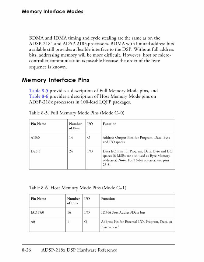
Memory Interface Modes
BDMA and IDMA timing and cycle stealing are the same as on the ADSP-2181 and ADSP-2183 processors. BDMA with limited address bits available still provides a flexible interface to the DSP. Without full address bits, addressing memory will be more difficult. However, host or micro-controller communication is possible because the order of the byte sequence is known.
Memory Interface PinsTable 8-5 provides a description of Full Memory Mode pins, and Table 8-6 provides a description of Host Memory Mode pins on ADSP-218x processors in 100-lead LQFP packages.
Table 8-5. Full Memory Mode Pins (Mode C=0)
Pin Name Number of Pins
I/O Function
A13:0 14 O Address Output Pins for Program, Data, Byte and I/O spaces
D23:0 24 I/O Data I/O Pins for Program, Data, Byte and I/O spaces (8 MSBs are also used as Byte Memory addresses) Note: For 16-bit accesses, use pins 23:8.
Table 8-6. Host Memory Mode Pins (Mode C=1)
Pin Name Number of Pins
I/O Function
IAD15:0 16 I/O IDMA Port Address/Data bus
A0 1 O Address Pin for External I/O, Program, Data, or
Byte access1
8-26 ADSP-218x DSP Hardware Reference

Memory Interface
D23:8 16 I/O Data I/O Pins for Program, Data Byte and I/O spaces
IWR 1 I IDMA Write Enable
IRD 1 I IDMA Read Enable
IAL 1 I IDMA Address Latch Pin
IS 1 I IDMA Select
IACK 1 O IDMA Port Acknowledge Configurable in Mode D; Open Drain
1 In Host Memory Mode, external peripheral addresses can be decoded using the A0, CMS, PMS, DMS, and IOMS signals.
Table 8-6. Host Memory Mode Pins (Mode C=1) (Cont’d)
Pin Name Number of Pins
I/O Function
ADSP-218x DSP Hardware Reference 8-27
Memory Interface Modes
8-28 ADSP-218x DSP Hardware Reference

9 DMA PORTSFigure 9-0.
Table 9-0.
Listing 9-0.
OverviewThe ADSP-218x processors include the following DMA interfaces:
• Byte Memory Space and Byte Memory DMA (BDMA) — The byte memory space can address up to 4M bytes. The BDMA inter-face supports booting from and runtime access to inexpensive 8-bit memories. The BDMA feature lets you define the number of mem-ory locations the BDMA interface transfers to or from internal memory in the background while the ADSP-218x DSP core contin-ues processing in the foreground.
• Internal Direct Memory Access (IDMA) Port —This 16-bit wide parallel port supports booting from and runtime access to host sys-tems (for example, PC Bus Interface ASICs). The DMA feature of this port lets you transfer data to/from internal memory in the back-ground while continuing foreground processing.
These DMA transfers are accomplished internally by “cycle stealing,” in the same way as serial port autobuffering. This means that the ADSP-218x processor uses internal bus cycles to transfer the data to and from memory. The stolen cycles only occur at instruction cycle boundaries — not between cycles of a multiple-cycle instruction. See “DMA Cycle Stealing, Hold Offs, and IACK Acknowledge” on page 9-47 for additional details.
ADSP-218x DSP Hardware Reference 9-1

BDMA Port
BDMA PortByte memory provides access to an 8-bit wide memory space through the BDMA port. The byte memory space provides access to 4 Mbytes of memory by utilizing 8 data lines as additional address lines. This gives the BDMA port an effective 22-bit address range. Figure 9-1 shows the ADSP-218x processor interface to BDMA.
Byte memory space consists of 256 pages, each containing 16 K x 8-bit wide locations. This memory can be written and read in four different for-mats: 24-bit, 16-bit, 8-bit MSB alignment, and 8-bit LSB alignment.
ADSP-218X Byte Mem ory(4 M x8)
BMS
RD
8
22
14
8
WR
D[16:23]
A[0:13]
D[8:15]
CS
OE
WE
A[0:21]
D[0:7]
Figure 9-1. ADSP-218x Processor BDMA Port Interface
9-2 ADSP-218x DSP Hardware Reference

DMA Ports
On powerup, the ADSP-218x processor can automatically load bootstrap code from byte memory. To use byte memory for purposes other than boot loading, such as runtime access to bulk data storage, you must know the following:
• 22-bit address that the code/data starts (BMPAGE, BEAD)
• Number of words (BWCOUNT) to read or write
• Word format (BTYPE) of the data
A BDMA transfer (non-boot loading) begins when data is written to the BWCOUNT register and completes when the BWCOUNT register decrements to zero. When the register reaches zero, a BDMA interrupt is issued.
There are no restrictions to the byte address alignment for BDMA accesses. The upper 8 bits of the address are from BMPAGE and the lower 14 bits are from BEAD. As the BDMA controller accesses memory, it automat-ically increments BMPAGE at page boundaries. Data or code can cross BMPAGE boundaries without a problem.
The following restrictions apply to BDMA transfers:
• The BDMA Internal Address register (BIAD) lets you set the 14-bit internal starting address for the BDMA transfer.
!To access the internal Program Memory and Data Memory Overlay regions for the ADSP-2187L, ADSP-2188M, and ADSP-2189M processors via BDMA, the BIAD register should be set to 0x2000-0x3fff for Program Memory Overlay regions and 0x0000-0x1fff for Data Memory Overlay regions. The BDMA Overlay bit field (bits 7:4 of the BDMA Control register) and the BTYPE field (bits 1:0 of the BDMA Control register) should also be set for the appropriate overlay regions.
• The BEAD or BIAD registers should not be accessed during BDMA transfers.
ADSP-218x DSP Hardware Reference 9-3

BDMA Port
• Other external memory accesses (PM Overlay, DM Overlay, or I/O space) take precedence over BDMA port accesses. These accesses cannot occur at the same time because they also use the processor’s external bus. (See “Priority Chain” on page 9-49 for more informa-tion.)
• Powerdown mode should not be entered with the BDMA port active. (See “Powerdown” in Chapter 7, “System Interface” for more information on powerdown restrictions.)
BDMA Port Functional DescriptionThe BDMA port lets you load or store program instructions and data from or to byte memory with very low processor overhead. While the ADSP-218x processor is executing program instructions, the BDMA port reads or writes code or data from or to byte memory—stealing one ADSP-218x processor cycle per word when it needs to write to or read from internal memory. You can calculate BDMA transfer time from the following formula:
1Cycle for Internal RD/WR
Number of PM or DMWords
Number of Bytesper Word
Number of AddedWait States per Byte
HoldOffs
+ ++
1 Cycle forTransfer
9-4 ADSP-218x DSP Hardware Reference

DMA Ports
If, for example, you wanted to transfer one hundred 24-bit program mem-ory words through the BDMA port, assuming five wait states and no hold offs, the operation would take 1900 cycles. This is shown in the following equation:
Hold offs for DMA transfers are defined in the section, “DMA Cycle Stealing, Hold Offs, and IACK Acknowledge” on page 9-47.
BDMA Control RegistersMemory-mapped registers are used to set up and control transfers through the BDMA port. Figures 9-2 through 9-7 show these registers.
The BDMA Internal Address register (BIAD) lets you set the 14-bit inter-nal starting address for the BDMA transfer. To access the internal Program Memory and Data Memory Overlay regions for all the ADSP-2187, ADSP-2188, and ADSP-2189 processors via BDMA, the BIAD register should be set to 0x2000-0x3fff for Program Memory Overlay regions and 0x0000-0x1fff for Data Memory Overlay regions. The BDMA Overlay bit field (bits 7:4 of the BDMA Control register) and the BTYPE field (bits 1:0 of the BDMA Control register) should also be set for the appropriate overlay regions.
1Cycle for Internal RD/WR
100 PM Words
3 Bytesper Word
5 AddedWait States per Byte
0HoldOffs
+ ++
1 Cycle forTransfer
ADSP-218x DSP Hardware Reference 9-5

BDMA Port
The BDMA Internal Address register (BIAD) lets you set the 14-bit inter-nal starting address for the BDMA transfer (see Figure 9-2). To access the internal Program Memory and Data Memory Overlay regions for all the ADSP-2187, ADSP-2188, and ADSP-2189 processors via BDMA, the BIAD register should be set to 0x2000-0x3fff for Program Memory Overlay regions and 0x0000-0x1fff for Data Memory Overlay regions. The BDMA Overlay (BMOVLAY) field (bits 7:4 of the BDMA Control register) and the BTYPE field (bits 1:0 of the BDMA Control register) should also be set for the appropriate overlay regions.
15 14 13 12 11 10 9 8 7 6 5 4 3 2 1 0
0 0 00 0 0 0 0 0 0 0 0 0 0 0 0
BDM A Internal Address
DM (0x3FE1)
BIAD
Note: Bits 14 and 15 a re unusedand should be set to 0.
Figure 9-2. BDMA Internal Address Register
9-6 ADSP-218x DSP Hardware Reference

DMA Ports
The BDMA External Address register (BEAD) lets you set the 14-bit exter-nal memory starting address for a BDMA transfer (see Figure 9-3). This register value represents the value of the address bits A[13:0], which are driven on the external address bus to your byte-wide device.
The BDMA port can access up to 4M bytes of information by using 22 bits of external addressing. These 22 bits are comprised of the following:
• Address bits 13:0, which correspond to the value of the BEAD register
• Address bits 21:14, which constitute the BMPAGE field (bits 15:8 of the BDMA Control register)
Table 9-1 lists the values driven onto the external bus for BDMA addressing.
Table 9-1. BDMA External Addresses
BDMA address DSP Pins Used BDMA Register Field
A21:A14 D23:D16 BDMA Control register bits 15:8 (BMPAGE)
A13:A0 A13:A0 BDMA External Address (BEAD) bits 13:8
15 14 13 12 11 10 9 8 7 6 5 4 3 2 1 0
0 0 00 0 0 0 0 0 0 0 0 0 0 0 0
BDM A External Address
DM (0x3FE2)
BEAD
Note: Bits 14 and 15 are unusedand should be set to 0.
Figure 9-3. BDMA External Address Register
ADSP-218x DSP Hardware Reference 9-7

BDMA Port
! BDMA transfers that cross BDMA page boundaries update the BMPAGE field of the BDMA Control register automatically.
BDMA Overlay bits (bits 7:4 of the BDMA Control register, shown in Figure 9-4) apply only to the ADSP-2187, ADSP-2188, and ADSP-2189 processors. These bits must be set to zero for all other ADSP-218x proces-sors (see Figure 9-5).
15 1 4 13 12 11 10 9 7 5 3 1
BMPAG E
BDMA Control
DM(0x3FE3)
BDIR
0 = load from BM1 = store to BM
BCR
0 = run during BDM A 1 = halt during BDMA,
Context Reset when done
BTYPE (See table)
BTYPE 00 01 10 11
Internal M emory Space PM D M DM DM
Word Size 24 16 8 8
Alignment Full Full MSB LSB word word
8 6 4 2 0
BMOVLAY
(ADSP-2187 , ADSP-2188, and ADSP-2189)
0 0 000 00 0 0 00 0 0 0 0
Figure 9-4. BDMA Control Register (ADSP-2187, ADSP-2188, and ADSP-2189)
9-8 ADSP-218x DSP Hardware Reference

DMA Ports
The BDMA Control register lets you set:
• BDMA Transfer Type (BTYPE)
• BDMA Direction (BDIR)
• BDMA Context Reset (BCR)
• Internal Overlay pages to be accessed by the BDMA transfer (applies to the ADSP-2187, ADSP-2188, and ADSP-2189 processors only)
• BDMA Page (BMPAGE)
15 1 4 13 12 11 10 9 7 5 3 1
BMPAG E
BDMA Control
DM(0x3FE3)
BDIR
0 = load from BM1 = store to BM
BCR
0 = run during BDM A 1 = halt during BDMA,
Context Reset when done
BTYPE (See table)
BTYPE 00 01 10 11
Internal M emory Space PM D M DM DM
Word Size 24 16 8 8
Alignment Full Full MSB LSB word word
8 6 4 2 0
(All ADSP-218x Processors except ADSP-2187, ADSP-2188, and ADSP-2189 )
000000000000000
Figure 9-5. BDMA Control Register (All ADSP-218x Processors except the ADSP-2187, ADSP-2188, and ADSP-2189)
ADSP-218x DSP Hardware Reference 9-9
BDMA Port
BTYPE can be:
• 00 24-bit Program Memory Words
• 01 16-bit Data Memory
• 10 8-bit bytes for Data Memory, MSB alignment
• 10 8-bit bytes for Data Memory, LSB alignment
BDIR can be:
• 0 from Byte Memory
• 1 to Byte Memory
BCR can be set to:
• 0 Allows program execution during BDMA
• 1 Inhibits program execution during BDMA transfers andcauses a context reset after transfer is complete
BMPAGE lets you select the starting page for BDMA transfer.
! Rebooting with BDMA Context Reset (BCR=1) is similar to a Pow-erup Context Reset. For more details on processor states during reset and reboot, see Chapter 7, “System Interface” in this manual.
The BWCOUNT register (shown in Figure 9-6) lets you start a BDMA transfer by writing the number of words for the transfer to this register. The count automatically decrements as the transfer proceeds. When the count is zero (i.e. transfer complete), the processor issues a BDMA interrupt. When MMAP and BMODE (ADSP-2181 and ADSP-2183 processors) or Mode B (all other processors) are set to zero on boot, a value of 32 (decimal) is written to this register directing the ADSP-218x processor to load the first 32 locations of its internal program memory.
9-10 ADSP-218x DSP Hardware Reference
DMA Ports
0 0 0 0 0 0 0 0 0 0 00 0 0 00
1 5 1 4 1 3 1 2 1 1 1 0 9 8 7 6 5 4 3 2 1 0
D M (0 x 3 F E 4 )
B D M A W o rd C o u n t
M M A P = 0 a n d B M O D E = 0 (A D S P -2 1 8 1 a n d A D S P -2 1 8 3 o n ly )
B W C O U N T
B W C O U N T
o r
D M (0 x 3 F E 4 )
M O D E B = 0 (A ll o th e r A D S P -2 1 8 x p ro c e s s o rs )
M M A P = 1 o r B M O D E = 1 (A D S P -2 1 8 1 a n d A D S P -2 1 8 3 o n ly )
M O D E B = 1 (A ll o th e r A D S P -2 1 8 x p ro c e s s o rs )
N o te : B its 1 4 a n d 1 5 a re u n u s e da n d s h o u ld b e s e t to 0 .
1 5 1 4 1 3 1 2 1 1 1 0 9 8 7 6 5 4 3 2 1 0
0 0 0 0 0 0 0 0 0 0 00 0 1 00
Figure 9-6. BDMA Word Count Register
ADSP-218x DSP Hardware Reference 9-11

BDMA Port
Two useful control techniques using this register are:
• Poll the BWCOUNT register to determine when the DMA transfer is complete (BWCOUNT=0) instead of waiting for the BDMA interrupt. The following code example illustrates this technique:
Poll_BWCOUNT:
ax0 = dm(0x3fe4); /* read value of BDMA count register */
ar = pass ax0; /* pass count value through ALU */
if eq jump BDMA_done; /* if count value = 0 then BDMA iscomplete */
jump Poll_BWCOUNT; /* else continue polling the BDMAcount register */
• Abort the DMA operation by writing a 1 to the BWCOUNT register and poll to determine when the transfer is complete (BWCOUNT=0) instead of waiting for the BDMA interrupt. (Note that the DMA transfer is aborted and cannot be resumed later.)
!Writing a zero to the BWCOUNT register results in 16 K words transferred.
BMWAIT consists of bits 12, 13, and 14 of the Composite Select Control register for all ADSP-218x processors except the M and N series (see Figure 9-7). For the M and N series processors, this field consists of bits 12, 13, 14, and 15 of the Composite Select Control register (see Figure 9-8). BMWAIT lets you select 0-7 wait states (each equal to a single instruction cycle) to apply to each byte memory access. BMWAIT is set to 7 after a reboot.
9-12 ADSP-218x DSP Hardware Reference

DMA Ports
0 1 1 1
BMWAIT
Composite Select Control
DM(0x3FE6)
15 14 13 12 11 10 9 8 7 6 5 4 3 2 1 0
(All ADSP-218x Processors except the M and N Series)
Figure 9-7. BMWAIT Field in Composite Select Control Register (All ADSP-218x Processors except the M and N Series)
BMWAIT
Composite Select Control
DM(0x3FE6)
15 14 13 12 11 10 9 8 7 6 5 4 3 2 1 0
1 1 1 1
(ADSP-218x M and N Series Processors)
Figure 9-8. BMWAIT Field in Composite Select Control Register (ADSP-218x M and N Series)
ADSP-218x DSP Hardware Reference 9-13
BDMA Port
Byte Memory Word FormatsIn your byte memory ROM or RAM, data is stored by the ADSP-218x PROM Splitter according to the data format you select: 24-bit program memory words, 16-bit data memory words, 8-bit data memory bytes with MSB-alignment, or 8-bit data memory bytes with LSB-alignment. The byte order for 24-bit program memory words and 16-bit data memory words stored in byte memory is most-significant-byte in the lower address. Table 9-1 shows an example of byte memory storage for all four code/data formats.
! BDMA transfers to/from internal memory are written to/stored from 16-bit wide locations. When transferring either of the data memory byte formats, the unused byte of Data Memory is zero-filled.
Table 9-2. Byte Memory Storage Formats
BTYPE Internal Memory Address
Internal Memory Contents
Byte Memory Address (page 0x00)
Byte MemoryContents
00 PM(0x0000) 0xABCDEF BM(0x0000)
BM(0x0001)
BM(0x0002)
0xAB
0xCD
0xEF
00 PM(0x0001) 0x123456 BM(0x0003)
BM(0x0004)
BM(0x0005)
0x12
0x34
0x56
01 DM(0x0000) 0x9876 BM(0x0006)
BM(0x0007)
0x98
0x76
01 DM(0x0001) 0x3456 BM(0x0008)
BM(0x0009)
0x34
0x56
9-14 ADSP-218x DSP Hardware Reference

DMA Ports
BDMA BootingThe ADSP-218x processor offers two methods for automatic booting after reset: BDMA booting and IDMA booting. This section describes BDMA booting. For information about IDMA booting, see “Boot Loading through the IDMA Port” on page 9-46.
When using BDMA booting, the entire on-chip program memory of an ADSP-218x processor, or any portion of it, can be loaded from an external source using a byte memory booting sequence. Table 9-3 shows how to select the post-reset booting method using the MMAP and BMODE pins on the ADSP-2181 and ADSP-2183 processors. Table 9-4 on page 9-16 shows how to select the post-reset booting method using the Mode D, Mode C, Mode B, and Mode A pins on all other processors.
! The Mode D pin is not available on the ADSP-2184, ADSP-2184L, ADSP-2185, ADSP-2185L, ADSP-2186, and ADSP-2186L proces-sors.
10 DM(0x0002) 0x9800 BM(0x000A) 0x98
10 DM(0x0003) 0x7600 BM(0x000B) 0x76
11 DM(0x0004) 0x0034 BM(0x000C) 0x34
11 DM(0x0005) 0x0056 BM(0x000D) 0x56
Table 9-2. Byte Memory Storage Formats
BTYPE Internal Memory Address
Internal Memory Contents
Byte Memory Address (page 0x00)
Byte MemoryContents
ADSP-218x DSP Hardware Reference 9-15
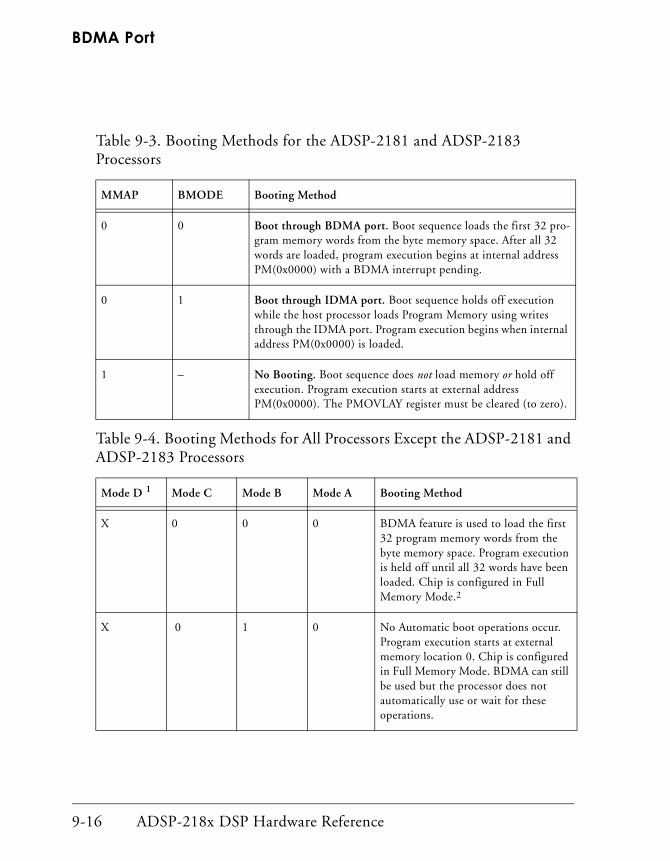
BDMA Port
Table 9-3. Booting Methods for the ADSP-2181 and ADSP-2183 Processors
MMAP BMODE Booting Method
0 0 Boot through BDMA port. Boot sequence loads the first 32 pro-gram memory words from the byte memory space. After all 32 words are loaded, program execution begins at internal address PM(0x0000) with a BDMA interrupt pending.
0 1 Boot through IDMA port. Boot sequence holds off execution while the host processor loads Program Memory using writes through the IDMA port. Program execution begins when internal address PM(0x0000) is loaded.
1 – No Booting. Boot sequence does not load memory or hold off execution. Program execution starts at external address PM(0x0000). The PMOVLAY register must be cleared (to zero).
Table 9-4. Booting Methods for All Processors Except the ADSP-2181 and ADSP-2183 Processors
Mode D 1 Mode C Mode B Mode A Booting Method
X 0 0 0 BDMA feature is used to load the first 32 program memory words from the byte memory space. Program execution is held off until all 32 words have been loaded. Chip is configured in Full Memory Mode.2
X 0 1 0 No Automatic boot operations occur. Program execution starts at external memory location 0. Chip is configured in Full Memory Mode. BDMA can still be used but the processor does not automatically use or wait for these operations.
9-16 ADSP-218x DSP Hardware Reference

DMA Ports
0 1 0 0 BDMA feature is used to load the first 32 program memory words from the byte memory space. Program execution is held off until all 32 words have been loaded. Chip is configured in Host Mode. IACK has active pulldown.
Note: Requires additional hardware.
0 1 0 1 IDMA feature is used to load any inter-nal memory as desired. Program execu-tion is held off until internal program memory location 0 is written to. Chip is configured in Host Mode. IACK has active pulldown.2
1 1 0 0 BDMA feature is used to load the first 32 program memory words from the byte memory space. Program execution is held off until all 32 words have been loaded. Chip is configured in Host Mode; IACK requires external pull-down.
Note: Requires additional hardware.
1 1 0 1 IDMA feature is used to load any inter-nal memory, as desired. Program execu-tion is held off until internal program memory location 0 is written to. Chip is configured in Host Mode. IACK requires external pulldown.
1 Mode D pin is not available on the ADSP-2184, ADSP-2184L, ADSP-2185, ADSP-2185L, AD-SP-2186, or ADSP-2186L processors.
2 Considered as standard operating settings. Using these configurations allows for easier design and better memory management.
Table 9-4. Booting Methods for All Processors Except the ADSP-2181 and ADSP-2183 Processors (Cont’d)
Mode D 1 Mode C Mode B Mode A Booting Method
ADSP-218x DSP Hardware Reference 9-17

BDMA Port
The ADSP-218x processors use a BDMA boot sequence after reset when the BMODE and MMAP pins equal 0 (ADSP-2181 and ADSP-2183 processors) or the Mode B pin equals 0 (all other ADSP-218x processors).
The BDMA port is initialized for booting as follows:
• BWCOUNT is set to 32
• BDIR, BMPAGE, BEAD, BIAD, and BTYPE are set to zero
• BCR is set to 1
• BMWAIT is set to 15 for the ADSP-218x M and N series processors and 7 for all other ADSP-218x processors
• BMOVLAY is set to 0 for the ADSP-2187, ADSP-2188, and ADSP-2189 processors
These initializations configure the BDMA port to load 32 Program Mem-ory words (96 bytes) (as specified by the BWCOUNT register) from Byte Memory Page zero (as specified in the BMPAGE field of the BDMA Control Register) and Byte Memory Address zero (as specified in the BEAD regis-ter) to internal Program Memory address zero (as specified in the BIAD register), using 24-bit Program Memory Word Format (as specified in the BTYPE field of the BDMA Control register).
When set to 1, the BDMA context reset bit (BCR) inhibits program execu-tion during BDMA transfer and causes execution to begin at address PM(0x0000) after the transfer is completed. For the ADSP-218x M and N series processors, the number of wait states (BMWAIT bits [15:12] of the Composite Select Control register) for BDMA accesses is set to the maxi-mum of 15. For all other ADSP-218x processors, the number of wait states (BMWAIT bits [14:12] of the Composite Select Control register) for BDMA accesses is set to the maximum value of 7. After the boot sequence is complete (32 words transferred), program execution begins at internal PM address 0x0000.
9-18 ADSP-218x DSP Hardware Reference

DMA Ports
The ADSP-218x PROM Splitter utility provides a boot loader option for ADSP-218x processor-based designs. See “Development Software Features for BDMA Booting” on page 9-20 for information.
If you are developing your own boot-loading software for ADSP-218x processors, however, you should note that the BDMA Context Reset bit (BCR) is set to 1 (inhibiting program execution during BDMA transfer) and a BDMA interrupt is pending (signalling the first 32 word were sent) after the boot sequence is complete. Your program will have to process the interrupt (if you unmask the BDMA interrupt with the IMASK register) or clear the interrupt (with the IFC register).
In an alternate method, using the BDMA interrupt without context clear, a loader program could suspend program execution with the IDLE instruc-tion while BDMA boot loading. If the loader sets the PM boot-load parameters, the loader enables only the BDMA interrupt in the IMASK reg-ister, and then executes an IDLE instruction. The IDLE instruction suspends program execution until the BDMA interrupt occurs. At that point all of program memory is loaded.
ADSP-218x DSP Hardware Reference 9-19

BDMA Port
Development Software Features for BDMA Booting
The ADSP-218x PROM Splitter utility lets you create BDMA boot-loader programs for ADSP-218x processor-based designs. This pro-vides a low overhead method for BDMA boot-loading your program. The boot loader program attaches memory loader code to the beginning of your executable program. The PROM Splitter generates loader code that initializes up to 6 pages of program memory and 4 pages of data memory, where each page is 16 K bytes in size. Typically, the code generated by the PROM Splitter is burned into an EPROM and used as the ADSP-218x’s Byte Memory space.
When the BMODE and MMAP pins equal 0 (ADSP-2181 and ADSP-2183 pro-cessors) or the Mode B pin equals 0 (all other ADSP-218x processors), the ADSP-218x processors loads the first 32 program memory words from the Byte memory space and then begins execution. The loader routine is in those first 32 words; it continues to load from the BDMA port until your whole program is loaded.
! For complete information on the PROM Splitter features, see the Linker & Utilities Manual for ADSP-218x & ADSP-219x Family DSPs and the software release notes.
9-20 ADSP-218x DSP Hardware Reference

DMA Ports
IDMA PortThe IDMA port is a separate port on the ADSP-2181 and ADSP-2183 processors and a configured port on all other ADSP-218x processors when they are in Host Mode (Mode C pin equals 1). It is a 16-bit parallel slave I/O port that allows the processor’s internal memory to be read or written by a host system. Figure 9-9 shows the ADSP-218x interface to the IDMA port.
The IDMA port is a gateway to all internal memory locations on the DSP (except for the processor’s memory-mapped control registers). The IDMA port is made up of 16 multiplexed data/address pins and 5 control pins. It provides transparent, direct access to the DSP’s on-chip program and data RAM. IDMA port read/write access is completely asynchronous and a host can access the DSP’s internal memory while the ADSP-218x proces-sor is operating at full speed.
ADSP-218x Host Processor
/
16
IS
IAL I/O FLAG PIN
MEMORY SELECT
IRD
IAD[0:15]
IWR
IACK
RD
WR
ACKNOWLED GE
D[0:15]
Figure 9-9. ADSP-218x Processor IDMA Port Interface
ADSP-218x DSP Hardware Reference 9-21

IDMA Port
The IDMA port does not require any ADSP-218x processor intervention to maintain data flow. The host system can access the ADSP-218x proces-sor’s internal memory directly, without going through a set of mailbox registers. Direct access to DSP memory increases throughput for block data transfers. Through the IDMA port, internal memory accesses can be performed with an overhead of one DSP processor cycle per word.
The ADSP-218x processor supports boot loading through the IDMA port, through the BDMA port, or from an external Program Memory Overlay. The MMAP and BMODE pins (ADSP-2181 and ADSP-2183 proces-sors) or Mode B pin (all other processors) select the DSP’s boot mode and memory map. Setting BMODE=1 and MMAP=0 (ADSP-2181 and ADSP-2183 processors) or Mode A=1 and Mode C=1 (all other ADSP-218x processors) directs the ADSP-218x to boot through the IDMA port. For information on IDMA booting, see “Boot Loading through the IDMA Port” on page 9-46.
! The IDMA port cannot be used to read or write the ADSP-218x’s memory-mapped control registers. For more information, see “Modifying Control Registers for IDMA” on page 9-31.
IDMA Port Pin SummaryTable 9-5 identifies and describes the IDMA port pins.
Table 9-5. IDMA Port Pins
Pin Name(s) Input/Output
Function
IRD I IDMA Port Read Strobe
IWR I IDMA Port Write Strobe
IS I IDMA Port Select
IAL I IDMA Port Address Latch Enable
9-22 ADSP-218x DSP Hardware Reference

DMA Ports
Four input signals control the IDMA port. Table 9-6 identifies and describes these signals.
An IDMA access ends when any one of the input signals goes inactive (high).
IAD0-15 I/O IDMA Port Address/Data Bus
IACK O IDMA Port Access Ready Acknowledge1
1 After reset, IACK is asserted (low). It stays low until an IDMA transfer is ini-tiated. After each IDMA operation is completed, IACK is again low.
Table 9-6. IDMA Port Input Signals
Input Signal Description
IDMA Port Select (IS) This signal acts as a chip select for all IDMA operations.
IDMA Read (IRD) When both the IS and IRD signals are active (low), an IDMA read cycle begins.
IDMA Write (IWR) When both the IS and IWR signals are active (low), an IDMA write cycle begins.
IDMA Address Latch (IAL) When the host wishes to initiate an Address Latch Sequence, this signal is asserted (active high). When the IS and IAL signals are both active, an IDMA Address Latch Sequence begins. At this point the host processor should drive the starting address of the IDMA transfer on the IAD bus.
Table 9-5. IDMA Port Pins (Cont’d)
Pin Name(s) Input/Output
Function
ADSP-218x DSP Hardware Reference 9-23

IDMA Port
Asserting the IDMA Port Select (IS) and address latch enable (IAL) directs the ADSP-218x processor to write the address on the IAD0-15 bus into the IDMA Control register. This register, shown in Figure 9-10, is mem-ory-mapped at address DM(0x3FE0). Note that the latched address (IDMAA) cannot be read back by the host.
Because the IDMA Control register is a memory mapped register, the address information can be written by either the host processor or the DSP itself. This allows more flexibility in your system design.
Because the ADSP-2187, ADSP-2188, and ADSP-2189 processors have additional on-chip overlay regions for Program Memory and Data Mem-ory, these processors contain an IDMA Overlay register that allows either the host or the DSP core to configure the specific overlay memory region to perform a DMA access. See Figure 9-13 on page 9-28. The ADSP-218x processors specified above can access this register at address 0x3FE7 in Data Memory. The host processor can access this register by performing an IDMA address latch cycle.
IDMA Control
DM(0x3FE0)
IDMAA
Starting address
IDMAD
Destination m emory type:
0=PM1=DM
15 14 13 12 11 10 9 8 7 6 5 4 3 2 1 0
U U U U U U U U U U UU U U U0
Figure 9-10. IDMA Control Register
9-24 ADSP-218x DSP Hardware Reference

DMA Ports
If bit 15 is set to 1 when performing an IDMA Address Latch Cycle, the data written on the IAD bus from the host will be written to the IDMA Overlay register. If bit 15 is set to zero when performing the Address Latch Cycle, the data written on the IAD bus from the host will be the IDMA starting address, which is written into the IDMAA bit field of the IDMA Control register.
Bits 3 through 0 of the IDMA Overlay register specify the PM Overlay page of the IDMA transfer. Program Memory Overlays are accessed via the IDMA port when the IDMA access is within the address range PM 0x2000 through PM 0x3fff. Bits 7 through 4 of the IDMA Overlay register specify the DM Overlay page of the IDMA transfer. Data Memory Overlays are accessed via the IDMA port when the IDMA access is within the address range DM 0x0000 through DM 0x1fff. These bit fields only apply to the ADSP-2187, ADSP-2188, and ADSP-2189 processors, due to their additional on-chip overlay memory regions. For all other ADSP-218x processors these bit fields do not apply and must be set to 0.
! When accessing the internal Program Memory and Data Memory Overlay regions of the ADSP-2187, ADSP-2188, and ADSP-2189 processors via the IDMA port, you must specify the target overlay region in the IDMA Overlay register prior to writing the target address to the 14-bit IDMAA starting address (bits [13:0]) of the IDMA Control register.
Please note the following:
• Core accesses to or from DM(0x3FE7) have bit 15 always cleared
• The IDMA port cannot access off-chip overlay pages directly
• There is no interaction between the IDMA OVLAY register and the core registers, PMOVLAY and DMOVLAY
ADSP-218x DSP Hardware Reference 9-25

IDMA Port
Through the IDMAA register, the DSP can also specify the starting address and data format for DMA operation. Asserting the IDMA port select (IS) and address latch enable (IAL) directs the DSP to write the address onto the IAD0-14 bus into the IDMA Control register. The address value is written on the bus by the host; then, the address information is written to or latched into the IDMA Address register (IDMAA). If bit 15 is set to 0, IDMA latches the address. If bit 15 is set to 1, IDMA latches into the OVLAY register.
The IDMA Address register, shown in Figure 9-11, is memory mapped at address DM (0x3FE0). Note that the latched address (IDMAA) cannot be read back by the host.
15 14 13 12 11 10 9 8 7 6 5 4 3 2 1 0
0 0 0 00 0 0 00 0 0
IDMA Overlay
DM(0x3FE7)
ID PMOV LAY
ID DMOV LAY
Note: The ID DMOVLAY and ID PMOVLAY bitfields app ly only to the ADSP-2187, ADSP-2188,and ADSP-2189 processors. For all otherADSP-218x processors, these bits are unusedand must be se t to 0.
Figure 9-11. IDMA Overlay Register
9-26 ADSP-218x DSP Hardware Reference
DMA Ports
Asserting the IDMA Port Select (IS) and Read strobe (IRD) inputs directs the ADSP-218x to output the contents of the memory location pointed to by the IDMA Control register onto the IDMA data bus.
Asserting the IDMA Port Select (IS) and Write strobe (IWR) inputs directs the ADSP-218x to write the input from the IDMA data bus to the address pointed to by the IDMA register.
When reading or writing to Data Memory, the IDMA data bus pins make up a 16-bit Data Memory word. When reading or writing to Program Memory, the upper 16 bits of the 24-bit Program Memory word are sent first on the IDMA data bus pins. On the next IDMA port read or write, the lowest 8 bits of the Program Memory word are sent on bits 0-7 of the IDMA data bus. For reads, the ADSP-218x processor sets data bus lines 8-15 to 0; for writes, the ADSP-218x processor ignores bits 8-15 from the host.
The IDMA Port Access Acknowledge (IACK) line identifies completion of data read/write operations. It also acts as a busy signal for the IDMA port. External devices must wait for this signal to go low before modifying the IDMA Control register or starting the next read or write operation.
ADSP-218x DSP Hardware Reference 9-27

IDMA Port
DMA Port Functional DescriptionThe IDMA port lets a host system directly access internal ADSP-218x memory locations (but not the memory-mapped control registers). Figure 9-11 shows a flow chart of the most general case for IDMA transfers.
H o s t s ta rts ID M A tra n s fe r .
H o s t c h e c k s IA C K c o n tro l lin eto s e e if th e D S P is " b u s y " .
H o s t u s e s IS a n d IA L c o n tro l lin e s tola tc h th e D M A s ta rtin g a d d re s s(ID M A A ) a n d P M /D M s e le c tio n in toth e D S P 's ID M A C o n tro l re g is te r .T h e D S P a ls o c a n s e t th e s ta rtin ga d d re s s a n d m e m o ry d e s tin a tio n .
H o s t u s e s IS a n d IR D (o r IW R ) t ore a d (o r w rite ) D S P in te rn a l m e m o ry(P M o r D M ).
H o s t e n d s ID M A tra n s fe r .
H o s t c h e c k s IA C K lin e t o s e e if t heD S P h a s c o m p le te d th e p re v io u sID M A o p e ra t io n .
C o n tin u e ?
Y e s
N o
Figure 9-13. General IDMA Transfer Flow Chart
9-28 ADSP-218x DSP Hardware Reference

DMA Ports
In the case shown in Figure 9-12, the host system starts an IDMA transfer by checking the state of the IACK line to determine port status (ready/busy). When the IDMA port is ready (when the IACK signal is low), the host directs the ADSP-218x (with the IS and IAL lines) to latch the IDMA internal memory address from the IDMA address/data bus to the IDMA Control register. Note that the latched address cannot be read back by the host.
Next, the host (using the IS and IRD or IS and IWR lines) begins reading (or writing) the DSP’s internal memory until done. With each IDMA read or write operation, the ADSP-218x automatically increments the IDMA internal memory address. Note that the ADSP-218x continues program execution throughout the IDMA transfer operation, except during the “stolen” cycle used to do the memory access.
! The IDMAA starting address field of the IDMA Control register wraps around when incrementing from addresses PM 0x3fff and DM 0x3fff. In other words, for the next IDMA access, the value for the IDMAA address field will point to address location PM 0x0000 or DM 0x0000.
The case shown in Figure 9-12 is not the only way to use the IDMA port. Some variations on this scheme include the following:
• After completing an IDMA port read/write operation, the host could change the IDMA internal memory address and start a new operation from a different starting address.
• After latching an IDMA internal memory address, the host could stop the operation and come back at a later time to proceed with the read/write operation. The IDMA starting memory address remains in the IDMA Control register until the host or DSP changes it.
• The ADSP-218x processor can also read and write the IDMA Con-trol register as part of your program. This means that the host could just control read/write operations and let the ADSP-218x processor control the IDMA starting memory address.
ADSP-218x DSP Hardware Reference 9-29
IDMA Port
• Using the IDMA short read cycle (which does not wait for the data-ready assertion of the IACK signal), you could set up a sin-gle-location data buffer for IDMA read transfers. For information on how this data buffer would work, see “Short Read Cycle” on page 9-37.
• For ADSP-218x applications with a host processor or host ASIC that does not use a data-ready or write-complete acknowledge, use the IDMA short read/write cycles.
There are some restrictions on IDMA operations. These hardware/soft-ware design restrictions include the following:
• If your design has both the host and ADSP-218x processors writing to the IDMA Control register, do not let both write to this register at the same time; the results of this are indeterminate.
• Host reads of internal Program Memory take two IDMA reads (for a 24-bit word through a 16-bit port). If an IDMA address latch cycle or an ADSP-218x processor write to the IDMA Control regis-ter occurs after the first Program Memory read cycle, the IDMA port “loses” the second half of the 24-bit Program Memory word. The next IDMA read or write uses the address selected by the new contents of the IDMA Control register. Note that writing to the IDMA Control register after the first half of a Program Memory IDMA read lets you read just 16-bit data from Program Memory.
• Host writes to internal Program Memory take two IDMA writes (for a 24-bit word through a 16-bit port). If an IDMA address latch cycle or a ADSP-218x write to the IDMA Control register occurs after a first Program Memory write cycle, the IDMA port “loses” the Program Memory word without changing the contents of memory. The next IDMA read or write accesses the address selected by the new contents of the IDMA Control register.
9-30 ADSP-218x DSP Hardware Reference

DMA Ports
• Host memory accesses through the IDMA port that occur while the ADSP-218x processor is in powerdown have some restrictions. See Chapter 7, “System Interface” for information on powerdown restrictions on IDMA port transfers.
Modifying Control Registers for IDMAThe ADSP-218x’s memory-mapped control registers are protected from DMA transfers to prevent accidental corruption. You may want the host processor to read and write these registers, however, in order to determine the ADSP-218x’s configuration and then change it.
To read the memory-mapped control registers, you must first transfer the contents of these locations to another area of internal RAM. Listing 9-1 shows a loop that performs this task:
Listing 9-1. Loop to Transfer Memory-Mapped Control Register Contents
#define NUM_REG 32
.section/dm Data_Memory;
.var temp_array[NUM_REG];
.section/pm Program_Code;i0 = temp_array; /* i0 points to 1st location of
buffer */l0 = 0; /* length of zero means
non-circular buffer */i1 = 0x3fe0; /* i1 points to 1st memory mapped
control register */l1 = 0; /* length of zero means
non-circular buffer */m1= 1; /* modify DAG registers by one
after each access */cntr = NUM_REG; /* counter equals number of
elements in buffer to beswapped */
ADSP-218x DSP Hardware Reference 9-31
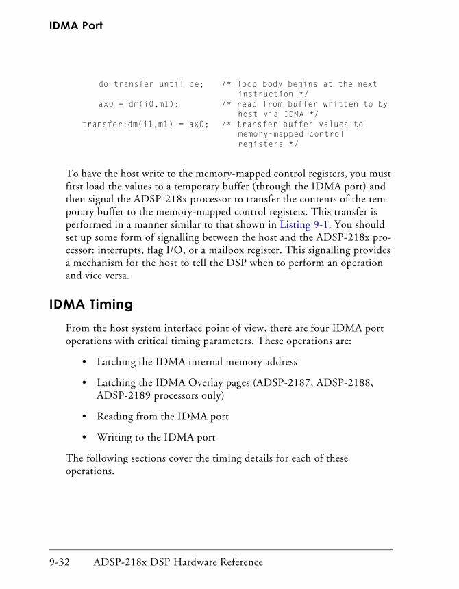
IDMA Port
do transfer until ce; /* loop body begins at the nextinstruction */
ax0 = dm(i0,m1); /* read from buffer written to byhost via IDMA */
transfer:dm(i1,m1) = ax0; /* transfer buffer values tomemory-mapped control registers */
To have the host write to the memory-mapped control registers, you must first load the values to a temporary buffer (through the IDMA port) and then signal the ADSP-218x processor to transfer the contents of the tem-porary buffer to the memory-mapped control registers. This transfer is performed in a manner similar to that shown in Listing 9-1. You should set up some form of signalling between the host and the ADSP-218x pro-cessor: interrupts, flag I/O, or a mailbox register. This signalling provides a mechanism for the host to tell the DSP when to perform an operation and vice versa.
IDMA TimingFrom the host system interface point of view, there are four IDMA port operations with critical timing parameters. These operations are:
• Latching the IDMA internal memory address
• Latching the IDMA Overlay pages (ADSP-2187, ADSP-2188, ADSP-2189 processors only)
• Reading from the IDMA port
• Writing to the IDMA port
The following sections cover the timing details for each of these operations.
9-32 ADSP-218x DSP Hardware Reference

DMA Ports
Address Latch Cycle
The host writes the DMA starting address and destination memory type (DM or PM) using the IDMA address latch cycle. The address latch cycle, shown in Figure 9-14, consists of the following steps:
1. Host ensures that IACK line is low.
2. Host asserts IAL and IS, directing the ADSP-218x processor to latch the IDMA starting address from the IAD15-0 address/data bus into the IDMA Control register.
3. Host drives the starting address (bits 13-0) and destination mem-ory type (bit 14) onto the IAD15-0 bus. Bit 15 must be a 0.
! The IRD and IWR remain high (inactive) throughout the latch oper-ation.
IACK
IAL
IS
IAD15-0 ADDRESS
The IDMA address valueis latched here on eitherthe rising edge of the ISsignal or the falling edgeof the IAL signal.
Figure 9-14. IDMA Address Latch or Overlay Latch Cycle
ADSP-218x DSP Hardware Reference 9-33

IDMA Port
! The IDMA starting address and destination memory type is avail-able to the host and to the ADSP-218x processor in the IDMA Con-trol register. For Data Memory accesses, the ADSP-218x processor increments the address automatically after each IDMA read or write transfer (16-bit word). For Program Memory accesses, the ADSP-218x processor increments the address automatically after each pair of IDMA read or write transfers (24-bit word).
" Both the ADSP-218x processor and the host can specify the starting address by writing to the IDMA Control register. Do not let the ADSP-218x processor access the IDMA Control register while it is being written by the host; this operation will have an indeterminate result.
Overlay Latch Cycle
The Overlay latch cycle applies only to the ADSP-2187L and all M and N series processors. The host writes the DMA starting address and destina-tion memory type (DM or PM) using the IDMA address latch cycle. The overlay latch cycle, shown in Figure 9-14 on page 9-33, consists of the fol-lowing steps:
1. Host ensures that IACK line is low.
2. Host asserts IAL and IS, directing the ADSP-218x processor to latch the IDMA Overlay pages from the IAD15-0 address/data bus into the IDMA Overlay register.
3. The host drives a 1 on bit 15, the DMOVLAY value on bits 7:4, and the PMOVLAY value on bits 3:0.
! The IRD and IWR remain high (inactive) throughout the latch oper-ation.
9-34 ADSP-218x DSP Hardware Reference

DMA Ports
Long Read Cycle
An IDMA long read cycle can be performed if your host processor uses a data-ready acknowledge signal to notify the host when to latch data on the IAD bus or if the host is configured to wait for the worst case data delay. A long read cycle could be used by a Motorola 68322 processor for example, where the IACK signal of the ADSP-218x processor would be connected to the DTACK signal of the Motorola 68322.
The host reads the contents of an ADSP-218x processor internal memory location using the IDMA port long read cycle. The read cycle, shown in Figure 9-15, consists of the following steps:
1. Host ensures that IACK line is low.
2. Host asserts IRD and IS (low), causing the ADSP-218x processor to put the contents of the location pointed to by the IDMA address on the IAD15-0 address/data bus.
3. ADSP-218x processor deasserts IACK line, indicating the requested data is being fetched. When the ADSP-218x processor asserts the IACK line, the requested data is driven on the IAD address/data bus.
4. Host detects the IACK line is now low and reads the data (Read Data) from the IAD15-0 address/data bus. (Alternately, the host can just wait a fixed worst case delay, which also guarantees the IACK signal is low again. After reading the data, the host deasserts IRD and IS.
! The IAL is low (inactive) and IWR is high (inactive) throughout the read operation.
ADSP-218x DSP Hardware Reference 9-35

IDMA Port
IDMA memory accesses “steal” one processor cycle, but they may only occur on instruction cycle boundaries. The best-case response for a 16-bit Data Memory read or the first 16 bits of a Program Memory read is 2.5 processor cycles; the worst case response is 3.5 cycles. One cycle is for syn-chronization, one is for reading the memory internally, and one-half cycle is for IACK setup time.
A second cycle of synchronization may be required. Thus the best-case and worst-case response times are determined as follows:
Best Case: 1 cycle (sync) + 1 cycle (internal memory read) + 0.5 cycle (IACK setup) = 2.5 cycles
Worst Case: 1 cycle (sync) + 1 cycle (sync) + 1 cycle (internal memory read) + 0.5 cycle (IACK setup) = 3.5 cycles
IACK
IS
IRD
IAD15-0 PREVIOUSDATA
READDATA
Host latches data here(at the falling edgeof the IACK signal).
Figure 9-15. IDMA Long Read Cycle
9-36 ADSP-218x DSP Hardware Reference

DMA Ports
In the case of a Program Memory operation, the second IDMA port read cycle for a given internal 24-bit word does not require an internal memory access, does not wait for an instruction cycle boundary, and takes 1.5 or 2.5 cycles.
The best- and worst-case response times given above assume no system hold offs. Hold offs for DMA transfers are defined in the section “DMA Cycle Stealing, Hold Offs, and IACK Acknowledge” on page 9-47.
" If an IDMA address latch cycle or an ADSP-218x processor write to the IDMA Control register occurs after a first Program Memory read cycle (16 bits), the IDMA port will lose the second half of the Program Memory word. The ADSP-218x processor treats the next IDMA access as the first operation for the new IDMA address and destination.
Short Read Cycle
Figure 9-16 on page 9-38 shows the host reading the contents of an ADSP-218x processor’s internal memory location using the IDMA short read cycle.The short read cycle can be used to allow the host to operate more quickly by not waiting for the internal access to complete. This method can be used if the host can do read accesses shorter than tIRDH1 and tIRDH2 and longer than tIRP1.
ADSP-218x DSP Hardware Reference 9-37

IDMA Port
The read cycle consists of the following steps:
1. Host ensures that IACK line is low.
2. Host asserts IRD and IS (low), directing the ADSP-218x processor to put the contents of the location pointed to by the target IDMA address on the IAD15-0 address/data bus.
3. ADSP-218x processor deasserts IACK line, indicating the requested data is being fetched.
4. The host asserts the IS and IRD signals for a minimum amount of time, adhering to the tIRP timing specification. The host then latches the Previous Data and deasserts the IS and IRD signals prior to tIRDH1or tIRDH2. (See the subsection entitled “IDMA Read, Short Read Cycle Timing” in the “Timing Parameters” section of the appropriate ADSP-218x processor data sheet.)
IA C K
IS
IR D
IA D 1 5 -0P R E V IO U SD A T A
D a ta is la tc h e d h e re .
t IR D H 1 o r t IR D H 2
If t h e I S o r IR D s ig n a ls a reh e ld a s s e rte d p a s t t hi s p oin t,th e d a ta c h a n g e s to th e n e x tR e a d D a ta .
t I IR P
Figure 9-16. IDMA Short Read Cycle
9-38 ADSP-218x DSP Hardware Reference
DMA Ports
! The host ignores the falling edge of the IACK signal, since the data is latched by the host on the rising edge of the IS or IRD signal not on the falling edge of the IACK signal.
The host must perform an initial “dummy read,” since the first short read access reads in the Read Data from the IAD bus. The next short read access reads in the first correct data word, Previous Data, on the IAD bus. The advantage of using short read accesses versus long read accesses is that short reads allow for shorter block transfer times.
! IAL is low (inactive) and IWR is high (inactive) throughout the read operation.
The IDMA short read and long read cycles provide different alternatives for implementing your DMA transfers. Short reads are useful for hosts that can handle the faster timing of these accesses, while long reads allow slower hosts more time.
The IDMA short read cycle also serves as a single-location data buffer. If you are using the ADSP-218x processor in a multiprocessing environ-ment, using this buffer is one way to avoid tying up the IAD bus (waiting for the IACK signal).
" If an IDMA address latch cycle or a ADSP-218x processor write to the IDMA Control register occurs after a first Program Memory read cycle, the IDMA port will lose the second half of the Program Memory word. The ADSP-218x processor treats the next host data on the IAD address/data bus as the new contents of the IDMA Con-trol register.
ADSP-218x DSP Hardware Reference 9-39

IDMA Port
IDMA Read—Short Read Only Mode
A new IDMA read mode cycle, Short Read Only Mode, has been added for the ADSP-218x M and N series processors. Because these processors are running at an increased clock rate (up to 75 MHz maximum for the M series processors and up to 80 MHz maximum for the N series processors), this increase in clock speeds has made the timing window for a host pro-cessor more critical when performing IDMA short read accesses.
To alleviate this timing constraint, the ADSP-218x M and N series pro-cessors provide support for an enhancement to the IDMA read cycle. The Short Read Cycle in Short Read Only Mode allows a host processor to read in only the Previous Data. This allows for longer timing duration on the IRD and IS signals by removing the maximum tIRDH1and tIRDH2 timing constraints. This increase in timing duration relieves the processor from complying with the tighter timing restrictions of the DSP. As shown in Figure 9-17, the IRD and IS signals can be held active indefinitely, allow-ing for the host processor to always latch in the Previous Data.
IACK
IS
IRD
IAD15-0 PREVIOUSDATA
Figure 9-17. IDMA Short Read Cycle in Short Read Only Mode Timing
9-40 ADSP-218x DSP Hardware Reference

DMA Ports
The Short Read Only mode can be enabled or disabled by setting or clear-ing bit 14 in the IDMA Overlay register. The default value for this bit (as well as the remaining bits in this control register) are shown in Figure 9-18.
! This bit applies to the ADSP-218x M and N series processors only. For all other ADSP-218x processors, this bit is unused and should be set to 0. Also, all bits shown in grey are reserved and must be set to 0.
Long Write Cycle
As with IDMA long read cycles, an IDMA long write cycle can be per-formed if your host processor uses a data-ready acknowledge signal to notify the host when to stop driving data on the IAD bus. A long write cycle could be used by a Motorola 68322 processor for example, where the IACK signal of the ADSP-218x processor would be connected to the DTACK signal of the Motorola 68322.
IDMA Overlay
DM(0x3FE7)
ID PMOVLAY
ID DMOVLAY
Short Read Only0=Disable1=Enable
15 14 13 12 11 10 9 8 7 6 5 4 3 2 1 0
0 0 0 00 0 0 00 0 0 0 0 00 0 0
ReservedSet to 0
ReservedSet to 0
Figure 9-18. IDMA Overlay Register (Short Read Only Mode)
ADSP-218x DSP Hardware Reference 9-41

IDMA Port
The host writes the contents of an internal memory location using the IDMA long write cycle. The write cycle, shown in Figure 9-19, consists of the following steps:
1. Host ensures that IACK line is low.
2. Host asserts IWR and IS (low), directing the ADSP-218x processor to write the data on the IAD15-0 address/data bus to the location pointed to by the target IDMA address.
3. ADSP-218x processor deasserts the IACK line, indicating it recog-nizes the IDMA write operation.
4. Host drives the data on the IAD address/data bus.
5. ADSP-218x processor asserts IACK line, indicating it latched the data on the IAD15-0 address/data bus.
6. Host recognizes the IACK line is now low, stops driving the data on the IDMA address/data bus and deasserts IWR and IS (ending the IDMA long write cycle).
Note that IAL is low (inactive) and IRD is high (inactive) throughout the write operation.
9-42 ADSP-218x DSP Hardware Reference

DMA Ports
! IDMA port writes to Program Memory require two IDMA port write cycles to write a word to ADSP-218x processor internal Pro-gram Memory. The ADSP-218x processor acknowledges the IDMA port write of the first 16 bits (MSBs of PM word) as they are written to a temporary holding latch, not waiting for an instruction cycle boundary. The ADSP-218x processor does not assert the IACK line after the second Program Memory write (or all Data Memory writes) until the internal memory write is complete and the IDMA port is ready for another transaction.
IACK
IS
IRD
IAD15-0DATA
Host stops drivingdata here.
Figure 9-19. IDMA Long Write Cycle
ADSP-218x DSP Hardware Reference 9-43

IDMA Port
" Host IDMA write accesses to internal Program Memory take two IDMA port writes (24-bit word through a 16-bit port). If an IDMA address latch cycle or a ADSP-218x processor write to the IDMA Control register occurs after a first program memory write cycle, the IDMA port “loses” the Program Memory word without changing the contents of ADSP-218x processor internal memory. The next IDMA read or write uses the address selected by the new contents of the IDMA Control register.
Short Write Cycle
An IDMA short write cycle should be performed if your host processor does not use a data-ready acknowledge signal to signify the completion of a write access.
The host writes the contents of a ADSP-218x processor internal memory location using the IDMA short write cycle. The write cycle, shown in Figure 9-20, consists of the following steps:
1. Host ensures that IACK line is low.
2. Host asserts IWR and IS (low), directing the ADSP-218x processor to write the data on the IAD15-0 address/data bus to the location pointed to by the target IDMA address.
3. ADSP-218x processor deasserts IACK line (high), indicating it rec-ognizes the IDMA write operation.
4. Host drives the data on the IAD address/data bus.
5. Host deasserts IWR and IS after meeting the short write timing requirements (ending the short write cycle).
6. ADSP-218x processor detects IWR and IS have gone high, then latches the data on the IAD address/data bus.
9-44 ADSP-218x DSP Hardware Reference

DMA Ports
7. Host stops driving the data on the IAD15-0 address/data bus after meeting the short write timing requirements. (See the tIRP timing specification in the subsection entitled “IDMA Read, Short Write Cycle” in the “Timing Parameters” section of the appropriate data sheet.)
! IAL is low (inactive) and IRD is high (inactive) throughout the write operation.
IDMA port writes to Program Memory require two IDMA port write cycles to write a word to ADSP-218x processor internal Program Memory. The ADSP-218x processor acknowledges the IDMA port write of the first 16 bits (MSBs of PM word) as they are written to a temporary holding latch.Writes to this holding latch are not done on an instruction cycle boundary. The ADSP-218x processor does not assert the IACK line (low) after the second Program Memory write (or all Data Memory writes) until the internal memory write is complete (performed on an instruction cycle boundary) and the IDMA port is ready for another transaction.
IACK
IS
IRD
IAD15-0DATA
Host stops drivingdata here.
Figure 9-20. IDMA Short Write Cycle
ADSP-218x DSP Hardware Reference 9-45

IDMA Port
" If an IDMA address latch cycle or a ADSP-218x processor write to the IDMA Control register occur after a first Program Memory write cycle, the IDMA port will lose the first half of the Program Memory word. The next Program Memory write will be considered the first half of a Program Memory write pair.
There are two features that differentiate the IDMA port long write from the IDMA short write. The long write supports hosts (processors or ASICs) that allow a data-written acknowledge. If your host needs the ADSP-218x processor to signal that it has written the data, use the IDMA long read cycle.
The short write lets your host hold data on the bus just until it is latched and then releases the bus. If you are using the ADSP-218x processor in a multiprocessing environment, using the short write is one way to avoid tying up the IAD15-0 data bus (waiting for the IACK signal). Short writes are also useful for hosts that can handle the short write timing but cannot extend the accesses with the IACK signal (when hold offs occur).
Boot Loading through the IDMA PortThe ADSP-218x processor supports boot loading through the IDMA port. To boot through the IDMA port, use the following steps:
• Reset the processor (assert RESET).
• Set MMAP=0 and BMODE=1 (ADSP-2181 and ADSP-2183 processors) or Mode A=1 and Mode C=1 (all other ADSP-218x processors). These pin settings select IDMA booting.
• Deassert RESET.
9-46 ADSP-218x DSP Hardware Reference

DMA Ports
• Load ADSP-218x processor internal memory through the IDMA port. Program execution is held off until you write to Program Memory address zero, PM(0x0000). The ADSP-218x processor responds to IDMA control signals (IAL, IS, IWR, and IRD) and pro-vides acknowledge (IACK) in the same manner as during non-boot-ing IDMA transfers.
• Write to PM(0x0000) to begin program execution.
"Make certain to load all of the necessary memory locations with the proper data before writing to PM 0x0000. When configured for an IDMA boot, the DSP core executes an IDLE instruction until PM 0x0000 is written to by the host via the IDMA port. Writing to this PM location forces the DSP to begin program execution from PM 0x0000.
DMA Cycle Stealing, Hold Offs, and IACK Acknowledge
ADSP-218x processors generate the IACK signal to notify the system that it is safe to read or write through the IDMA port. After reset, IACK is asserted (low). It stays low until an IDMA transfer is initiated. After each IDMA operation is completed, the IACK signal will again be low.
In order for IACK to be asserted (low) during the IDMA operation, the IDMA port must have completed the internal memory access by either writing data to memory or reading data from memory. The IDMA port must “steal” a processor cycle to do this. In order to steal a processor cycle, the IDMA port must wait for an instruction completion boundary. Thus if IACK is not asserted, it is not safe for the host to access the IDMA port.
ADSP-218x DSP Hardware Reference 9-47

IDMA Port
In most cases, there is an instruction boundary on every clock cycle (CLKOUT period) and the IDMA port can complete its transfer in a given period of time. There are, however, some situations where either the ADSP-218x processor does not complete an instruction in one clock cycle or the IDMA port cannot access memory. These situations are called DMA hold offs. The following describes DMA hold-off situations:
• Bus Request — If the ADSP-218x processor is being held in Bus Request when it attempts an external access (DM Overlay, PM Overlay, or I/O memory space), or if it is not in Go mode, processor execution stops in the middle of the cycle and no instruction bound-ary is encountered. Therefore, the IDMA port cannot complete its internal memory access and IACK will be held off.
• External Access with Wait State(s) — If the ADSP-218x processor is performing a wait-stated external access (DM Overlay, PM Over-lay, or I/O memory space), then the instruction cycle will not com-plete until the access has completed; the IDMA port cannot steal a cycle, and IACK will be held off.
• Multiple External Accesses — If the ADSP-218x processor is exe-cuting a multifunction instruction where more than one of the required elements (PM instruction fetch, PM data access, or DM data access) resides externally, it will require more than one cycle to complete the instruction and IACK will be held off. Likewise, if the ADSP-218x processor is executing an instruction from external PM that initiates an I/O memory space access, IACK will be held off until the cycle completes.
• IDLE n (clock-reducing IDLE instruction) — Because this instruc-tion slows down the effective cycle time of the ADSP-218x proces-sor, IACK may be delayed.
9-48 ADSP-218x DSP Hardware Reference

DMA Ports
• SPORT Autobuffering to External Memory with Wait Stated Access — When one of the processor’s serial ports needs to access external memory for autobuffering and the external access takes more than one cycle, the IDMA transfer will be held off.
• EZ-ICE Emulation — When the EZ-ICE emulator is controlling your ADSP-218x processor target system, IDMA transfers may be held off for periods of time.
Priority Chain
The ADSP-218x processor priority chain for concurrent requests occur-ring at instruction cycle boundaries is as follows:
1. Completion of an external memory access
2. IDMA internal memory transfers
3. BDMA internal memory transfers
4. SPORT autobuffer operations
5. Emulator interrupt
6. Emulator instruction
7. Powerdown interrupt
8. Unmasked interrupt
9. Normal instruction execution
Using the IACK signal simplifies your system design by allowing you to ignore hold-off conditions. If you always wait for IACK to assert before accessing the IDMA port, the DMA transfers will always operate properly.
ADSP-218x DSP Hardware Reference 9-49

IDMA Port
You can ignore IACK, however, if you are sure that no hold-offs occur in your system or if your IDMA accesses are longer than any hold-offs. To be sure of this, you must carefully analyze all possible hold-off conditions of your system.
9-50 ADSP-218x DSP Hardware Reference

10 HARDWARE INTERFACING AND EXAMPLES
Figure 10-0.
Table 10-0.
Listing 10-0.
OverviewThis chapter contains two major sections: Interfacing to DSP Processors and Interfacing Examples. The Interfacing to DSP Processors section provides detailed information about interfacing ADSP-218x family processors to analog-to digital converters (ADCs), digital-to-analog converters (DACs) and coder/decoders (codecs). The Interfacing Examples section provides some simple examples of interfacing ADSP-218x family processors to ADCs, DACs, and codecs.
Interfacing to DSP ProcessorsCurrent technology offers highly integrated DSPs that contain on-chip ADCs and DACs, as well as the DSP itself. These integrated DSPs elimi-nate most of the interface problems of separate components. Additionally, stand-alone ADCs and DACs are now available with interfaces especially designed for DSP chips, thereby minimizing or eliminating external inter-face support or glue logic.
High performance sigma-delta ADCs and DACs are currently available separately or in the same package (called a codec). Some examples of codecs include the AD73311 and AD73322. These products are also designed to require minimum glue logic when interfacing to the most common DSP chips. This section discusses the various data transfer and timing issues associated with ADCs, DACs, and codecs.
ADSP-218x DSP Hardware Reference 10-1

Interfacing to DSP Processors
Parallel Interfacing to DSP ProcessorsInterfacing an ADC or a DAC to a fast DSP via a parallel interface requires an understanding of how the DSP processor reads data from a memory-mapped peripheral (the ADC) and how the DSP processor writes data to a memory-mapped peripheral (the DAC). We will first consider some general timing requirements for reading and writing data. It should be noted that the same concepts presented here regarding ADCs and DACs apply equally when reading and writing from/to external memory.
Reading Data from Memory-Mapped ADCs
Figure 10-1 provides a block diagram for a typical parallel DSP interface to an external ADC. This diagram has been greatly simplified to show only those signals associated with reading data from an external mem-ory-mapped peripheral device.
RD
IRQ
IOMSADDRE SS
DECODE
SAMPLIN G
CLOCK
1
2
4 5
6
7
M EMOR YADDRES S BUS
INPUT/OUTPUT
PROCESSOR
INTERRU PT
REQUES T
M EMORY READ
M EMORY DATA
A0-A11
D8-D23
ADSP-218X DAC
CONVERT START
CHIP S ELECT
CONVERSION
COMPLETE
OUTPUT ENABLE
OUTPUT DATA
3
M EMORY SELE CT
BUS
8
Figure 10-1. ADC to ADSP-218x DSP Parallel Interface
10-2 ADSP-218x DSP Hardware Reference

Hardware Interfacing and Examples
Figure 10-2 shows the timing diagram for the ADSP-218x read-cycle.
In this example, it is assumed that the ADC is sampling at a continuous rate which is controlled by the external sampling clock, not the internal DSP clock. Using a separate clock for the ADC is the preferred method, since the DSP clock may be noisy and introduce jitter in the ADC sam-pling process, thereby increasing the noise level.
Assertion of the sampling clock at the ADC convert start input initiates the conversion process (step 1). The leading (or trailing) edge of this pulse causes the internal ADC sample-and-hold to switch from the sampling mode to the hold mode so that the conversion process can take place.
DSP
CLKOUT
A0-A11
IOMS
RD
D8-D23
t AS R
t CRD t R P
t RDA
t RW R
t RDH t AA
t RDD
Figure 10-2. ADSP-218x DSP Memory Read Timing
ADSP-218x DSP Hardware Reference 10-3

Interfacing to DSP Processors
When the conversion is complete, the conversion complete output of the ADC is asserted (step 2). The read process thus begins when this signal is applied to the processor interrupt request line (IRQ) of the DSP. The pro-cessor then places the address of the peripheral initiating the interrupt request (the ADC) on the memory address bus (A13- A0) (step 3). At the same time, the processor asserts a memory select line (IOMS is shown here) (step 4).
The two internal address buses of the ADSP-218x (Program Memory address bus and Data Memory address bus) share a single external address bus, and the two internal data buses (program memory data bus and data memory data bus) share a single external data bus. The boot memory select (BMS), data memory select (DMS), program memory select (PMS), and input/output memory select (IOMS) signals indicate which memory space the external buses are being used for. These signals are typically used to enable an external address decoder as shown in Figure 10-1. The output of the address decoder drives the chip select input of the peripheral device (step 5).
The memory read (RD) is asserted tASR ns after the IOMS line is asserted (step 6). The sum of the address decode delay plus the peripheral chip select setup time should be less than tASR in order to take full advantage of the RD low-time. The RD line remains low for tRP ns. The memory read signal is used to enable the three-state parallel data outputs of the peripheral device (step 7). The RD line is connected to the appropriate pin on the peripheral device usually called output enable or read. The rising edge of the RD sig-nal is used to clock the data on the data bus into the DSP processor (step 8). After the rising edge of the RD signal, the data on the data bus must remain valid for tRDH ns, the data hold time. In the case of most members of the ADSP-218x family, this specification value is 0 ns.
10-4 ADSP-218x DSP Hardware Reference

Hardware Interfacing and Examples
The following list provides the key requirements for a parallel peripheral device read interface. Values are given for the ADSP-2189M DSP operat-ing at 75 MHz.
• Peripheral device data outputs must be three-state compatible.
• Address decode delay plus peripheral chip select setup time must be less than address and memory select setup time tASR (0.325 ns min-imum for an ADSP-2189M DSP).
• For zero wait-state access, the time from a negative-going edge of read signal (RD) to output data valid must be less than tRDD (1.65 ns maximum for an ADSP-2189M DSP operating at 75 MHz). Oth-erwise, software wait states must be added or processor clock fre-quency reduced.
• Output data from the peripheral must remain valid for tRDH from the rising edge of read signal (RD) (0 ns for the ADSP-2189M).
• The peripheral device must accept minimum output enable pulse width of tRP (3.65 ns for ADSP-2189M operating at 75 MHz). Otherwise, software wait states must be added or processor clock frequency reduced.
The DSP tRDD specification determines the peripheral device data access time requirement. In the case of the ADSP-2189M, tRDD = 1.65 ns mini-mum at 75 MHz. If the access time of the peripheral is greater than this, wait states must be added or the processor speed reduced. This is a rela-tively common situation when interfacing external memory or ADCs to fast DSPs.
ADSP-218x DSP Hardware Reference 10-5
Interfacing to DSP Processors
The following equations provide the relationship between these timing parameters for the ADSP-2189M (these specifications are dependent on the DSP clock frequency):
• tCK = Processor Clock Period (13.3 ns)
• tASR = Address and Memory Select Setup before Read Low = 0.25tCK – 3 ns minimum
• tRDD = Read Low to Data Valid = 0.5 tCK – 5 ns + # wait states x tCK maximum
• tRDH = Data Hold from Read High = 0 ns minimum
• tRP= Read Pulse Width = 0.5 tCK – 3ns + # wait states x tCK minimum
The ADSP-2189M processor can be interfaced easily to slow peripheral devices, using its programmable wait state generation capability. Three registers control wait state generation for boot, program, data and I/O memory spaces. You can specify 0 to 15 wait states for each parallel mem-ory interface. Each added wait state increases the allowable external data memory access time by an amount equal to the processor clock period (13.3 ns for the ADSP-2189M operating at 75 MHz). In this example, the I/O memory address, IOMS, and RD lines are all held stable for an additional amount of time equal to the duration of the wait states.
The AD7854/AD7854L is an example of ADCs that operated in parallel mode. It is a 12 bit, 200/100 KSPS ADC. It operates on a single +3 V to +5.5 V supply and dissipates only 5.5 mW (+3 V supply, AD7854L). An automatic powerdown after conversion feature reduces this to 650 µW.
10-6 ADSP-218x DSP Hardware Reference
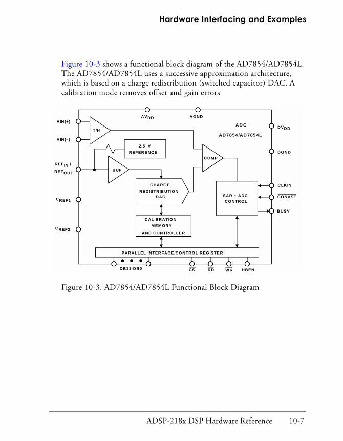
Hardware Interfacing and Examples
Figure 10-3 shows a functional block diagram of the AD7854/AD7854L. The AD7854/AD7854L uses a successive approximation architecture, which is based on a charge redistribution (switched capacitor) DAC. A calibration mode removes offset and gain errors.
T/H
COMP
2.5 V
REFER ENCE
CHARGE
REDISTRIB UTIONDAC SAR + ADC
CONTROL
PARALLEL INTERFAC E/CONTROL REGISTER
CALIBRATIO N
MEMORY
AND CONTRO LLER
AVDD AGNDAIN(+)
AIN(–)
REFIN /
REFOUT
CREF1
DB11-DB0 CS RD WR HBEN
DVDD
DGND
CLKIN
CONVST
BUSY
AD7854 /AD7854L
BUF
CREF2
ADC
Figure 10-3. AD7854/AD7854L Functional Block Diagram
ADSP-218x DSP Hardware Reference 10-7

Interfacing to DSP Processors
The key interface timing specifications for the AD7854/AD7854L and the ADSP-2189M are compared in Table 10-1. Specifications for the ADSP-2189M are given for a clock frequency of 75 MHz.
Examining the timing specifications shown in Table 10-1reveals that for the timing between the devices to be compatible, 5 software wait states must be programmed into the ADSP-2189M. This increases tRDD to 68.15 ns, which is greater than the data access time of the AD7854/AD7854L (t8 = 50 ns maximum). The read pulse, tRP, is likewise increased to 70.15 ns, which meets the ADC’s read pulse width require-ment (t7 = 70 ns minimum). Unless the memory-mapped peripheral has an extremely short access time, wait states are generally required, whether interfacing to ADCs, DACs, or external memory.
Table 10-1. Parallel Read Interface Timing Specification Comparison between the ADSP-2189M and AD7854/AD7854L
ADSP-2189M Processor (75 MHz) AD7854/AD7854L ADC
tASR (Data Address Memory Select Setup Time
before RD Low) = 0.325 ns minimum
t5 (CS to RD Setup Time) = 0 ns minimum
(Must add Address Decode Time to this value)
1tRP (RD Pulse Width) = 3.65 ns + # wait
states x 13.3 ns minimum = 70.15 ns mini-mum
1 Adding 5 wait states to the ADSP-2189M DSP increases tRP to 70.15 ns, which is greater than t7 (70 ns) and meets the t8 (50 ns) requirement.
t7 (RD Pulse Width) = 70 ns minimum
tRDD (RD Low to Data Valid) = 1.65 ns + #
wait states x 13.3 ns minimum = 68.15 ns minimum
t8 (Data Access Time after RD) = 50 ns maxi-
mum
tRDH (Data Hold from RD High) = 0 ns mini-
mum
2t9 (Bus Relinquish Time after RD) = 5 ns
minimum/40 ns maximum
2 t9 maximum (40 ns) may cause bus contention if a write cycle immediately follows the read cycle.
10-8 ADSP-218x DSP Hardware Reference

Hardware Interfacing and Examples
A simplified interface diagram for the two devices is shown in Figure 10-4. The conversion complete signal from the AD7854/AD7854L corresponds to the BUSY output pin. Notice that the configuration allows the DSP to write data to the AD7854/AD7854L parallel interface control register. This is needed in order to set various options in the AD7854/AD7854L and perform the calibration routines. In normal operation, however, data is read from the AD7854/AD7854L as described above. Writing to exter-nal parallel memory-mapped peripherals is discussed in the next section, “Writing Data to Memory-Mapped DACs”,
R D
IR Q
D M S
D 23-D 8
AD S P-2 18 9M
75 M Hz
A 0
W R
S A M P LIN G
C LO C K
AD 7 854 /A D 785 4L
A D C
C O N V ST
C S
B U S Y
R D
D B 1 1-D B 0
H B E N
W R
5 so ftw a re w a it s tates
H B E N a nd W R req uired for w riting to A D C
S am pling c loc k m ay com e fro m D S P
(LO W = R E A D D B 11-D B 0)
D A T A
N otes:
D S P
Figure 10-4. AD7854/AD7854L ADC Parallel Interface to ADSP-2189M
ADSP-218x DSP Hardware Reference 10-9

Interfacing to DSP Processors
Parallel interfaces between other DSP processors and external peripherals can be designed in a similar manner by carefully examining the timing specifications for all appropriate signals for each device. The data sheets for most ADCs contain sufficient information in the application section to interface them to the DSPs.
Writing Data to Memory-Mapped DACs
Figure 10-5 shows a simplified block diagram of a typical DSP interface to a parallel peripheral device (such as the DAC shown in this figure).
RD
IRQ
IOMSADDRE SS
DECODE
SAMPLING
CLOCK
1
3 5
4
6
MEMORYADDRESS BUS
INPUT/OUTPUT
PROCESSOR
INTERRUPT
REQUEST
MEMORY READ
MEMORY DATA
A0-A11
D8-D23
ADSP-218X DAC
DAC LATCHSTROBE
CHIP SELECT
INPUT LATCHSTROBE
PARALLEL DATAINPUT
2
MEMORY SELE CT
BUS
7
1
Figure 10-5. DAC to ADSP-218x DSP Parallel Interface
10-10 ADSP-218x DSP Hardware Reference

Hardware Interfacing and Examples
Figure 10-6 shows the memory-write cycle timing diagram for the ADSP-21xx-family.
In most real-time applications, the DAC is operated continuously from a stable sampling clock. Most DACs for these applications have double buffering: an input latch to handle the asynchronous DSP interface, fol-lowed by a second latch (called the DAC latch), which drives the DAC current switches. The DAC latch strobe is derived from an external stable sampling clock. In addition to clocking the DAC latch, the DAC latch strobe is also used to generate a processor interrupt to the DSP, which indicates that the DAC is ready for a new input data word.
DSP
CLKO UT
A0-A11
IO M S
W R
D8-D23
tW P
tD WtW D E
tC W R
tA S W
tA W
tD H tD D R
tW W R
tW R A
Figure 10-6. ADSP-218x DSP Memory Write Timing
ADSP-218x DSP Hardware Reference 10-11

Interfacing to DSP Processors
The write process is thus initiated by the peripheral device asserting the DSP interrupt request line. This indicates that the peripheral device is ready to accept a new parallel data word (step 1). The DSP then places the address of the peripheral device on the address bus (step 2) and asserts a memory select line (DMS is shown here) (step 3). This causes the output of the address decoder to assert the chip select input to the peripheral (step 5). The write (WR) output of the DSP is asserted tASW ns after the negative-going edge of the DMS signal (step 4). The width of the WR pulse is tWP ns. Data is placed on the data bus (D) and is valid tDW ns before the WR line goes high (step 6). The positive-going transition of the WR line is used to clock the data on the data bus (D) into the external parallel mem-ory (step 7). The data on the data bus remains valid for tDH ns after the positive-going edge of the WR signal.
The following is a list of key requirements for a parallel peripheral device write interface. The key specification is tWP, the write pulse width.
• Address decode delay plus peripheral chip select setup time must be less than the address and memory select setup time tASW (0.325 ns for the ADSP-2189M processor operating at 75 MHz).
• For zero wait-state access, input data setup time must be less than tDW (2.65 ns for the ADSP-2189M processor operating at 75 MHz). Otherwise, software wait states must be added or processor clock frequency reduced.
• Input data hold time must be less than tDH (2.325 ns for the ADSP-2189M processor operating at 75 MHz).
• The peripheral device must accept input write clock pulse width tWP (3.65 ns minimum for the ADSP-2189M processor operating at 75 MHz). Otherwise, software wait states must be added or proces-sor clock frequency reduced.
10-12 ADSP-218x DSP Hardware Reference

Hardware Interfacing and Examples
! All but the fastest peripheral devices require wait states to be added due to their longer data access times.
The following equations show the key timing specifications for the ADSP-2189M. Note that they are all related to the processor clock frequency.
• tCK = Processor Clock Period (13.3 ns)
• tASW = Address and Memory Select Setup before WR Low = 0.25tCK – 3 ns minimum
• tDW = Data Setup before WR High = 0.5 tCK – 4 ns + # wait states x tCK
• tDH = Data Hold after WR High = 0.25 tCK – 1 ns
• tWP= WR Pulse Width = 0.5 tCK – 3ns + # wait states x tCK minimum
Another parallel device is the AD5340. It is a 12-bit 100 KSPS DAC with a parallel data interface. It operates on a single +2.5 V to +5.5 V supply and dissipates only 345 µW (+ 3V supply). A powerdown mode further reduces the power to 0.24 µW.
ADSP-218x DSP Hardware Reference 10-13

Interfacing to DSP Processors
The AD5340 incorporates an on-chip output buffer that can drive the output to both supply rails. The AD5340 allows the choice of a buffered or unbuffered reference input. The device has a poweron reset circuit that ensures that the DAC output powers on at 0 V and remains there until valid data is written to the device. Figure 10-7 shows a block diagram of the AD5340.The input is double buffered.
INPUTREGISTER
DACREGISTER
12-BIT
DAC
POWERDOWNLOGIC
INT
ER
FA
CE
LO
GIC
DB11
DB0
BUF
GAIN
CS
WR
CLR
LDAC
VREF
VOUT
PD GND
RESET
BUF
POWERONRESET
Figure 10-7. AD5340 Parallel Input DAC
10-14 ADSP-218x DSP Hardware Reference

Hardware Interfacing and Examples
Table 10-2 compares the key interface timing specifications for the ADSP-2189M DSP and the AD5340 DAC. Specifications for the ADSP-2189M are given for a clock frequency of 75 MHz.
Note: Adding 2 wait states to the ADSP-2189M DSP increases tWP to 30.25 ns and tDW to 29.25 ns,
which is greater than t3 (20 ns) and t4 (5 ns), respectively.
Examining the timing specifications shown in Table 10-2 reveals that for the timing between the devices to be compatible, two software wait states must be programmed into the ADSP-2189M processor. This increases the width of WR to 30.25 ns, which is greater than the minimum required by the AD5340 write pulse width (20 ns). The data setup time of 5 ns for the AD5340 is also met by adding two wait states. A simplified interface dia-gram for the two devices is shown in Figure 10-8.
Table 10-2. Parallel Write Interface Timing Specification Comparison between the ADSP-2189M DSP and AD5340 DAC
ADSP-2189M Processor (75 MHz) AD5340 DAC
tASW (Address and Data Memory Select Setup
Time before WR Low) = 0.325 ns minimum
t1 (CS to RD Setup Time) = 0 ns minimum
tWP (WR Pulse Width) = 3.65 ns + # wait states
x 13.3 ns minimum =30.25 ns minimum
t3 (WR Pulse Width) = 20 ns minimum
tDW (Data Setup before WR High) = 2.65 ns +
# wait states x 13.3 ns minimum = 29.25 ns minimum
t4 (DataValid to WR Setup Time) = 5 ns maxi-
mum
tDH (Data Hold after WR High) = 2.325 ns
minimum
t5 (DataValid to WR Hold Time) = 4.5 ns
minimum
ADSP-218x DSP Hardware Reference 10-15

Interfacing to DSP Processors
Parallel interfaces with other DSP processors can be designed in a similar manner by carefully examining the timing specifications for all appropri-ate signals for each device.
Serial Interfacing to DSP ProcessorsDSP processors that have serial ports, such as the ADSP-218x family, pro-vide a simple interface to peripheral ADCs and DACs. Use of the serial port eliminates the need for using large parallel buses to connect the ADCs and DACs to the DSP.
IRQ
DMS
SAMPLIN G
CLOCK
D8-D19
ADSP-2189M
75 MHZ
LDAC
CS
DB0-DB11
WR
AD5340
DAC
Notes:2 software wait statesSampling c lock m ay come from the DSP
DSP
WR
Figure 10-8. AD5340 DAC Parallel Interface to ADSP-2189M
10-16 ADSP-218x DSP Hardware Reference

Hardware Interfacing and Examples
In order to understand serial data transfer better, we will first examine the serial port operation of the ADSP-218x series. A block diagram of one of the two serial ports (SPORTs) of the ADSP-218x is shown in Figure 10-9.
The transmit (TX) and receive (RX) registers are not memory mapped, but they are identified by name in the ADSP-218x assembly language. For SPORT0, the transmit and receive registers are named TX0 and RX0, respectively. For SPORT1, these registers are named TX1 and RX1, respectively.
TXn
TRANSMIT DATA
REGISTER
TRANSMIT SHIFT
REGISTER
COMPANDING
HARDWARE
(µ-LAW OR A-LAW)
RXn
RECEIVE DATA
REGISTER
SERIAL
CONTROL
INTERNAL
GENERATO R
RECEIVE SHIFT
REGIST ER
DT TFS SCLK RFS DR
DMD BUS
16
16
16
16
16
Polarity of TFS and RFS
is software programm able CLOCK
SERIAL
Figure 10-9. ADSP-218x Family Serial Port Block Diagram
ADSP-218x DSP Hardware Reference 10-17
Interfacing to DSP Processors
In the receiving portion of the serial port, the receive frame sync (RFS) sig-nal initiates reception. The serial receive data (DR) from the external device (ADC) is transferred into the receive shift register one bit at a time. The negative-going edge of the serial clock (SCLK) is used to clock the serial data from the external device into the receive shift register. When a com-plete word has been received, it is written to the receive data register (RX), and the receive interrupt for that serial port is generated. The receive data register is then read by the processor.
Writing to the transmit data register (TX) readies the serial port for trans-mission. The transmit frame sync (TFS) signal initiates transmission. The value in the TX register is then written to the internal transmit shift regis-ter. The data in the transmit shift register is sent to the peripheral device (DAC) one bit at a time, and the positive-going edge of the serial clock (SCLK) is used to clock the serial transmit data (DT) into the external device. When the first bit has been transferred, the serial port generates the transmit interrupt. The transmit data register can then be written with new data, even though the transmission of the previous data is not complete.
In the normal framing mode, the frame sync signal (RFS or TFS) is checked at the falling edge of SCLK. If the framing signal is asserted, data is avail-able (transmit mode) or latched (receive mode) on the next falling edge of SCLK. The framing signal is not checked again until the word has been transmitted or received.
In the alternate framing mode, the framing signal is asserted in the same SCLK cycle as the first bit of a word. The data bits are latched on the falling edge of SCLK, but the framing signal is checked only on the first bit. Inter-nally-generated framing signals remain asserted for the length of the serial word.
! The alternate framing mode of the serial port in the ADSP-218x is normally used to receive data from ADCs and transmit data to DACs.
10-18 ADSP-218x DSP Hardware Reference
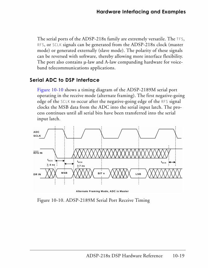
Hardware Interfacing and Examples
The serial ports of the ADSP-218x family are extremely versatile. The TFS, RFS, or SCLK signals can be generated from the ADSP-218x clock (master mode) or generated externally (slave mode). The polarity of these signals can be reversed with software, thereby allowing more interface flexibility. The port also contains µ-law and A-law companding hardware for voice-band telecommunications applications.
Serial ADC to DSP Interface
Figure 10-10 shows a timing diagram of the ADSP-2189M serial port operating in the receive mode (alternate framing). The first negative-going edge of the SCLK to occur after the negative-going edge of the RFS signal clocks the MSB data from the ADC into the serial input latch. The pro-cess continues until all serial bits have been transferred into the serial input latch.
MSB BIT n LSB
ADC
SCLK
RFS IN
DR IN
tSC S
4 ns 7 ns
Alternate Framing M ode, ADC is Master
> >
tSCH tS C S
Figure 10-10. ADSP-2189M Serial Port Receive Timing
ADSP-218x DSP Hardware Reference 10-19

Interfacing to DSP Processors
The key timing specifications of concern are the serial data setup (tSCS) and hold times (tSCH) with respect to the negative-going edge of the SCLK. In the case of the ADSP-2189M, these values are 4 ns and 7 ns, respec-tively. The latest generation ADCs with high speed serial clocks will have no trouble meeting these specifications, even at the maximum serial data transfer rate.
The AD7853/AD7853L is a 12 bit, 200/100 KSPS ADC which operates on a single +3 V to +5.5 V supply and dissipates only 4.5 mW (+3 V sup-ply, AD7853L). After each conversion, the device automatically powers down to 25 µW. The AD7853/AD7853L is based on a successive approxi-mation architecture and uses a charge redistribution (switched capacitor) DAC. A calibration feature removes gain and offset errors.
Figure 10-11 shows a block diagram of the AD7853/AD7853L.
COMP
2.5 V
REFERENCE
CHARGE
REDISTRIBUTIONDAC
SAR + ADC
CONTROL
SERIAL INTERFACE/CONTROL REGISTER
CALIBRATION
MEMORYAND CONTROLLER
AVDD AGNDAIN(+)
AIN(–)
REFIN/
REFOUT
CREF1
DVDD
DGND
CLKIN
CONVST
BUSY
AD7853L
BUF
CAL
AGND
SLEEP
SM1 SM2 SYNC DIN DOUT SCLK POLARITY
T/H
CREF2
Figure 10-11. AD7853/AD7853L ADC Serial Output
10-20 ADSP-218x DSP Hardware Reference

Hardware Interfacing and Examples
The AD7853 operates on a 4 MHz maximum external clock frequency. The AD7853L operates on a 1.8 MHz maximum external clock frequency. Figure 10-12 shows the timing diagram for AD7853L.
The AD7853/AD7853L ADCs have external mode pins, SM1 and SM2, which configure the SYNC and SCLK signals as inputs or outputs. In the examples shown in Figure 10-11 and Figure 10-12, the SYNC and SCLK sig-nals are generated internally by the AD7853L.
The AD7853L serial clock operates at a maximum frequency of 1.8 MHz (556 ns period). The data bits are valid 330 ns after the positive-going edges of SCLK. This allows a setup time of approximately 330 ns minimum before the negative-going edges of SCLK, which easily meets the ADSP-2189M 4 ns tSCS requirement.
The hold-time after the negative-going edge of SCLK is approximately 226 ns, which again easily meets the ADSP-2189M 7 ns tSCH timing require-ment. These simple calculations show that the data and RFS setup and hold requirements of the ADSP-2189M are met with considerable margin.
DB15 DB0
SCLK
(O/P)
SYNC (O/P)
DB11
1 5 6 16
556 ns
330 ns M IN
226 ns
THREE-STATE THREE-STATE
DOUT (O/P)
Figure 10-12. AD7853L ADC Serial Output Timing
ADSP-218x DSP Hardware Reference 10-21

Interfacing to DSP Processors
Figure 10-13 shows the AD7853L interfaced to the ADSP-2189M and connected in a mode to transmit data from the ADC to the DSP (alter-nate/master mode).
The AD7853/AD7853L contains internal registers that can be accessed by writing from the DSP to the ADC via the serial port. These registers are used to set various modes in the AD7853/AD7853L as well as to initiate the calibration routines. These connections are not shown in the diagram.
DR
RFS
SCLK
CLOCK
INPUT
4 MHz/1.8 MHz MAX
ADSP-2189M
75 M Hz
DSPCLKIN
SCLK
DOUT
AD7853 /AD7853L
ADC
SYNC
SERIAL
PORT
SAMPLING
CLOCK
(OPTIONAL)CONVST
Figure 10-13. AD7853/AD7853L ADC Serial Interface to ADSP-2189M
10-22 ADSP-218x DSP Hardware Reference

Hardware Interfacing and Examples
Serial DAC to DSP Interface
Interfacing serial input DACs to the serial ports of DSPs , such as the ADSP-218x family, is also relatively straightforward and similar to the pre-vious discussion regarding serial output ADCs. The details will not be repeated here, but a simple interface example will be shown.
The AD5322 is a 12-bit, 100 KSPS dual DAC with a serial input inter-face. It operates on a single +2.5 V to +5.5 V supply. Figure 10-14 shows a block diagram of the AD5322.
Power dissipation on a +3 V supply is 690 µW. A powerdown feature reduces this to 0.15 µW. Total harmonic distortion is greater than 70 dB below full scale for a 10 kHz output.
I
NT
ER
FA
CE
LO
GIC
INPUT
REGISTER A
DAC STRING
DAC A
RESISTOR
NETWORK
INPUT DAC STRING
DAC B
RESISTOR
NETWORK
POW ER-DO WN
LOGIC
SYNC
SCLK
DIN
VDD VREFAPOW ERON
RESET
LDAC VREFBGND
AD5322
VOUTAREGISTER A
VOUTBREGISTER B REGISTER B
Figure 10-14. AD5322 Dual DAC
ADSP-218x DSP Hardware Reference 10-23
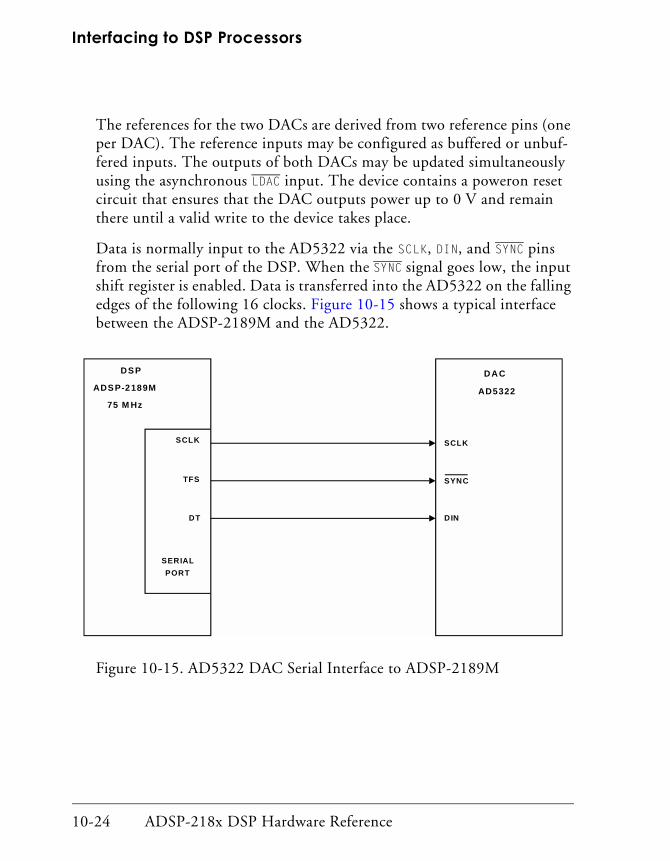
Interfacing to DSP Processors
The references for the two DACs are derived from two reference pins (one per DAC). The reference inputs may be configured as buffered or unbuf-fered inputs. The outputs of both DACs may be updated simultaneously using the asynchronous LDAC input. The device contains a poweron reset circuit that ensures that the DAC outputs power up to 0 V and remain there until a valid write to the device takes place.
Data is normally input to the AD5322 via the SCLK, DIN, and SYNC pins from the serial port of the DSP. When the SYNC signal goes low, the input shift register is enabled. Data is transferred into the AD5322 on the falling edges of the following 16 clocks. Figure 10-15 shows a typical interface between the ADSP-2189M and the AD5322.
DT
TFS
SCLK
ADSP-2189M
75 M Hz
SCLK
DIN
AD5322
DAC
SYNC
SERIAL
PORT
DSP
Figure 10-15. AD5322 DAC Serial Interface to ADSP-2189M
10-24 ADSP-218x DSP Hardware Reference

Hardware Interfacing and Examples
Notice that the clocks to the AD5322 are generated from the ADSP-2189M clock. It is also possible to generate the SCLK and SYNC sig-nals externally to the AD5322 and use them to drive the ADSP-2189M. The serial interface of the AD5322 is not fast enough to handle the ADSP-2189M maximum master clock frequency. However, the serial interface clocks are programmable and can be set to generate the proper timing for fast or slow DACs.
The input shift register in the AD5322 is 16 bits wide. This 16-bit word consists of four control bits followed by 12 bits of DAC data. The first bit loaded determines whether the data is for DAC A or DAC B. The second bit determines if the reference input will be buffered or unbuffered. The next two bits control the operating modes of the DAC (normal, power-down with 1 kΩ to ground, powerdown with 100 kΩ to ground, or powerdown with a high impedance output).
Interfacing I/O Ports, Analog Front Ends, and Codecs
Since most DSP applications require both an ADC and a DAC, I/O Ports and codecs have been developed that integrate the two functions on a sin-gle chip as well as provide easy-to-use interfaces to standard DSPs. These chips also go by the name of analog front ends (AFEs).
An example of an analog front end is the AD73322. This device is a dual analog front end with two 16-bit ADCs and two 16-bit DACs and is capa-ble of sampling at 64 KSPS. It is designed for general purpose applications, including speech and telephony using sigma-delta ADCs and sigma-delta DACs. Each channel provides 77 dB signal-to-noise ratio over a voiceband signal bandwidth.
ADSP-218x DSP Hardware Reference 10-25

Interfacing to DSP Processors
Figure 10-16 shows a functional block diagram of the AD73322.
The ADC and DAC channels feature programmable input/output gains with ranges of 38 dB and 21 dB, respectively. An on-chip voltage refer-ence is included to allow single supply operation on +2.7 V to +5.5 V. Power dissipation is 73 mW with a +3 V supply.
The sampling rate of the codecs is programmable with four separate set-tings of 64 kHz, 32 kHz, 16 kHz, and 8 kHz when operating from a master clock of 16.384 MHz.
ΣΣΣΣ ∆ ∆ ∆ ∆ ADC
CHANNEL 1
ΣΣΣΣ ∆ ∆ ∆ ∆ DAC
REFERENCESERIAL
PORT
VFBP1
VINP1
VINN1
VFBN1
VFBP2
VINP2
VINN2
VFBN2
REFOUT
REFCAP
VOUTP1
VOUTN1
VOUTP2
SDI
SDIFS
SCLK
SE
RESET
MCLK
SDOFS
SDO
AVDD1 AVDD2
AGND1 AGND2 DGND
CHANNEL 1
CHANNEL 2
CHANNEL 2
ΣΣΣΣ ∆ ∆ ∆ ∆ ADC
ΣΣΣΣ ∆ ∆ ∆ ∆ DAC
DVDD
VOUTN2
Figure 10-16. AD73322 Codec with Serial Interface
10-26 ADSP-218x DSP Hardware Reference

Hardware Interfacing and Examples
The serial port allows easy interfacing of single or cascaded devices to industry standard DSP engines, such as the ADSP-218x family. The SPORT transfer rate is programmable to allow interfacing to both fast and slow DSP engines. Figure 10-17 shows the AD73322 interface to the ADSP-218x family.
The SE pin (SPORT enable) may be controlled from a parallel output pin or a flag pin, such as FL1; or, where SPORT powerdown is not required, it can be permanently strapped high using a suitable pull-up resistor. The RESET pin may be connected to the system hardware reset, or it may be controlled with another flag bit.
SDIFS
SDI
SCLK
SDO
SDOFS
RESET
SE
TFS
DT
SCLK
DR
RFS
FL0
FL1
ADSP-218x
DSP
AD73322
CO DEC
SE
SCLK
SDOFS
SDO
SDIFS
SDI
ADC SAM PLE WORD, DEVICE 2
CLOCK
16.384 M Hz
ADC SAM PLE WORD, DEVICE 1
DAC DATA WORD, DEVICE 2 DAC DATA WORD, DEVICE 1
Figure 10-17. AD73322 Interface to ADSP-218x Family Processors
ADSP-218x DSP Hardware Reference 10-27

Interfacing to DSP Processors
In the program mode, data is transferred from the DSP to the AD73322 control registers to set up the device for desired operation. Once the device has been configured by programming the correct settings to the various control registers, the device may exit the program mode and enter the data mode. The dual ADC data is transmitted to the DSP in two blocks of 16-bit words. Similarly, the dual DAC data is transmitted from the DSP to the AD73322 in two blocks of 16-bit words. Simplified inter-face timing is also shown in Figure 10-17.
The AD73422 is the first product in the dspConverter™ family of prod-ucts that integrate a dual analog front end (AD73322) and a DSP (52 MIPS ADSP-2185L/ADSP-2186L). The entire functionality of the dual-channel codec and the DSP fits into a small, 119-ball 14 mm by 22 mm plastic ball grid array (PBGA) package. The obvious advantage of this size package is the saving of circuit board real estate. ADC and DAC sig-nal-to-noise ratios are approximately 77 dB over voiceband frequencies.
The AD74222-80 integrates 80 K bytes of on-chip memory configured as 16 K words (24-bit) of program RAM, and 16 K words (16-bit) of data RAM. The AD73422-40 integrates 40 K bytes of on-chip memory config-ured as 8 K words (24-bit) of program RAM, and 8 K words (16-bit) of data RAM. Powerdown circuitry is also provided to meet the low power needs of battery operated portable equipment. The AD73422 operates on a +3 V supply and dissipates approximately 120 mW with all functions operational.
The following summarizes the features of the ADSP73422 dspConverter™:
• Complete dual codec (AD73322) and DSP (ADSP-2185L/ADSP-2186L)
• 14 mm by 22 mm BGA package
• +3 V single-supply operations, 73 mW power dissipation
• Powerdown mode
10-28 ADSP-218x DSP Hardware Reference

Hardware Interfacing and Examples
• Codec
• Dual 16-bit sigma-delta ADCs and DACs
• Data rates: 8, 16, 32, 64 KSPS
• 77 dB SNR
• DSP
• 52 MIPS
• ADSP-218x code compatible
• 80 K byte and 40 K byte on-chip memory options
High-Speed InterfacingWith the advent of ever faster DSP clock rates and newer architectures it has become possible to acquire and process high speed signals. The pro-grammability of DSPs makes it possible to run different algorithms on the same hardware while providing different system functionality.
An example of high-speed ADC is the AD9201. It is a dual-channel, 10-bit, 20 MSPS ADC that operates on a single +2.7 V to +5.5 V supply and dissipates only 215 mW (+3 V supply). The AD9201 offers closely matched ADCs needed for many applications, such as I/Q communica-tions. Input buffers, an internal voltage reference and multiplexed, digital, output buffers make interfacing to the AD9201 very simple.
The companion part to the AD9201 ADC is the AD9761 DAC. The AD9761 is a dual, 10-bit, 20 MSPS per channel DAC operating on a sin-gle +2.7 V to +5.5 V supply and dissipating only 200 mW (+3 V supply). A voltage reference, digital latches and 2x interpolation make the AD9761 useful for I/Q transmitter applications.
ADSP-218x DSP Hardware Reference 10-29

Interfacing to DSP Processors
Figure 10-18 shows a simplified ADSP-218x system connected to the AD9201 ADC and the AD9761 DAC. The ADC and DAC both have parallel interfaces connected to the external port of the DSP.
Due to the simple interface between the DSP processor and the AD9201 and AD9761, shown in Figure 10-18, a memory select signal is not required. When performing reads from the ADC, only the RD signal is required to assert the chip select of the AD9201. Writes require only the use of the WR signal to the AD9761. If additional peripherals are to be interfaced to the DSP's external bus, some external decoding logic would be required.
AD9201
ADC
D0-D9
CLOCK
SELECT
CHIP-SELECT
ADSP-218X
SCLK
A0
RD
WR
AD9761
DAC
CLOCK
WRITE
SELECT
DUAL 10-BIT20 MSPS ADCs
DUAL 10-BIT20 MSPS DACs
D0-D9
D8-D17
DSP
Figure 10-18. AD9201 ADC and AD9761 DAC Interface to ADSP-218x
10-30 ADSP-218x DSP Hardware Reference

Hardware Interfacing and Examples
DSP System InterfaceFigure 10-19 shows a simplified ADSP-2189M system using the full memory mode configuration with two serial devices, a byte-wide EPROM, and optional external program and data overlay memories.
Programmable wait state generation allows the fast processor to connect easily to slower peripheral devices. The ADSP-2189M also provides four external interrupts, seven general-purpose input/output pins, and two serial ports.
ADDR
DATA
BMS
WR
RD
IOMS
PMS
DMS
CMS
14
24
2214
8 ADDR
DATA
CS
8
11
16ADDR
DATA
CS
14
24ADDR
DATA
BYTE
MEMORY
I/O SPACE
(PERIPHERALS)
2048 LOCATIONS
OVERLAY
MEMORY
TWO 8 K PM SEG MENTS
1/2 X CLOCKOR CRYSTAL
CLKIN
XTAL
SERIALDEVICE
5
SERIAL
DEVICE
5
SPORT1
SPORT0
ADSP-2189M
IRQ x 4
7 PFx/MODE x
BR
BG
BGH
PWD
PWDACK
INTERRUPTS
PROGRAM MABLE
IO PINS
BUS/REQ UEST/GRANT/HUNG
POWER DOW N INPUT
POWER DOWN OUTPUT
TWO 8 K DM SEGMENTS
Figure 10-19. ADSP-2189M System Interface (Full Memory Mode)
ADSP-218x DSP Hardware Reference 10-31
Interfacing Examples
SPORT1 can alternately be configured as two additional interrupts (IRQ0 and IRQ1), a general-purpose input pin (FI), a general purpose output pin (FO), and the serial clock (SCLK). This alternate configuration provides a total of six external interrupts (excluding the non-maskable powerdown interrupt signal, which can also be used as an external interrupt), eight programmable I/O pins, one dedicated input pin, one dedicated output pin, and one serial port.
The ADSP-2189M can also be operated in the Host Memory mode, which allows access to the full external data bus but limits addressing to a single address bit. Additional system peripherals can be added in the Host Memory mode through the use of external hardware to generate and latch address signals.
Interfacing ExamplesThis section provides some hardware examples of circuits that can be interfaced to the ADSP-218x DSP serial ports or DMA ports. As with any hardware design, it is important that timing information be carefully ana-lyzed. Therefore, the appropriate ADSP-218x processor data sheet should be used in addition to the information presented in this chapter.
Serial Port to Codec InterfaceThe ADSP-218x family processors may be interfaced, via the serial ports, to most common codec’s. An example is shown Figure 10-20, using the AD73311 codec. Up to eight, AD73311 codec’s, may be connected in a cascade configuration to obtain multiple channel operation.
When two or more codec’s are connected in a cascade configuration, it is necessary to synchronously enable the serial ports and bring all codecs out of reset simultaneously to ensure correct operation of the serial interface. Figure 10-20 illustrates this process.
10-32 ADSP-218x DSP Hardware Reference
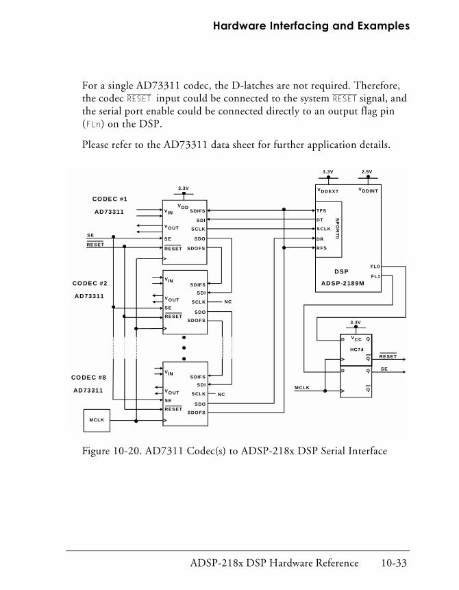
Hardware Interfacing and Examples
For a single AD73311 codec, the D-latches are not required. Therefore, the codec RESET input could be connected to the system RESET signal, and the serial port enable could be connected directly to an output flag pin (FLn) on the DSP.
Please refer to the AD73311 data sheet for further application details.
RESET
RESET
TFS
DSP
ADSP-2189M
FL0
NC
MCLK
D Q
Q
D Q
Q
HC74
VDD
VOUT
SE
VIN SDIFS
SDI
SCLK
SDO
SDOFS
VOUT
SE
VINSDIFS
SDI
SCLK
SDO
SDOFS
SDIFS
SDI
SCLK
SDO
SDOFSRESET
VOUT
SE
VIN
VDDEXT VDDINT
VCC
RESET
SE
3.3V
3.3V
3.3V
2.5V
CO DEC #1
AD73311
RESET
SE
CO DEC #2
AD73311
CO DEC #8
AD73311 M CLK
FL1
SCLK
DT
DR
RFS
SP
OR
T0
NC
Figure 10-20. AD7311 Codec(s) to ADSP-218x DSP Serial Interface
ADSP-218x DSP Hardware Reference 10-33

Interfacing Examples
Serial Port to ADC InterfaceThis section provides the following two examples of a serial port to ADC interface:
• ADSP-218x DSP SPORT to AD7475/95 ADC interface
• ADSP-218x DSP SPORT to AD7888 ADC interface
ADSP-218x DSP to AD7475/95 ADC Interface
The ADSP-218x DSP SPORT can be interfaced to the AD7475/95 ADC, as shown in Figure 10-21. Note that the RFS pin is configured as an out-put on the DSP and is used to initiate conversion in the ADC. It is also used to determine the sample rate.
SCLK
DR
DT
RFS
TFS
SCLK
SDATA
CS
DSP
ADSP-218MADC
AD7475/95
VINA
VDRIVE
3.3V
GND
VREF
GND
2.5V
VDD
5V
M AX 1MS/s
SP
OR
T0
VDDEXT VDDINT
Figure 10-21. ADSP-218x DSP to AD7475/95 ADC Serial Interface
10-34 ADSP-218x DSP Hardware Reference

Hardware Interfacing and Examples
Figure 10-22 shows the serial timing for the ADSP-218x DSP interface to the AD7475/95 ADC.
Using a DSP CLKIN frequency of 36 MHz, the CLKOUT frequency will be 72 MHz. For the correct serial interface timing, the DSP SPORT Control registers should be set up as follows:
Note that the DSP RFS frame sync output is used to initiate conversion and set the sample rate. For some applications, it may be desirable to use a more stable frequency source, such as an independent clock. In this case, the external clock would be an input to both the CS pin on the ADC and the DSP RFS frame sync pin.
SPORTn Control Register, DM (0x3FF6): 0x7DCF
SPORTn SCLKDIV Register, DM (0x3FF5): 0x0001
SPORTn RFSDIV Register, DM (0x3FF4): 0x0011
CS (RFS)
SDATA 0 0 0 0 M SB LSB
SCLK
0
1 2 3 4 5 16 17 18 1
ONE COM PLETE SERIAL FRAME – M AX SAM PLE RATE 1M S/s
– SCLK=18M Hz
Figure 10-22. ADSP-218x DSP to AD7475/95 ADC Serial Interface Timing
ADSP-218x DSP Hardware Reference 10-35

Interfacing Examples
ADSP-218x DSP to AD7888 ADC interface
Using the 8-channel AD7888 ADC, it is possible to sample eight indepen-dent analog inputs. Figure 10-23 shows the serial interface used. Note that there is also a data line from the DSP to the ADC. This data line is used to send channel select and power management information to configure internal ADC registers.
SCLK
DR
DT
RFS
TFS
SCLK
DOUT
DIN
CS
DSP
ADSP-2189M
ADC
AD7888
8Ch, 12-Bit, 125KS/s
AIN1
AIN8
3.3V
AGND AGND
VREF
GND
2.5V
3.3V
VDD
VDDEXT VDDINT
SP
OR
T0
Figure 10-23. ADSP-218x DSP to AD7888 ADC Serial Interface
10-36 ADSP-218x DSP Hardware Reference

Hardware Interfacing and Examples
Figure 10-24 shows the serial interface timing for the ADSP-218x DSP to AD7888 ADC Interface.
Using a DSP CLKIN frequency of 36 MHz, the CLKOUT frequency will be 72 MHz. For the correct serial interface timing, the DSP SPORT Control registers should be set up as follows:
Note that the DSP RFS frame sync output is used to initiate conversion and set the sample rate. For some applications, a more accurate clock may be needed to set the sample rate and minimize jitter. In this case, the external clock would be an input to both the CS pin on the ADC and the DSP RFS frame sync pin.
SPORTn Control Register, DM(0x3FF6): 0x7DCF
SPORTn SCLKDIV Register, DM (0x3FF5): 0x0011
SPORTn RFSDIV Register, DM (0x3FF4): 0x000F
SCLK
CS (RFS)
DIN
DOUT
DO N TC ZE RO AD D R 2 AD D R 1 AD D R 0 RE F PM 1 PM 0
0 0 0 0 MS B LS B
DO N TC
0
1 2 3 4 5 6 16 1
ONE COM PLETE SERIAL FRAME. M AX SAM PLE RATE, 135kS/s: SCLK=2MHz M AX
Figure 10-24. ADSP-218x DSP to AD7888 ADC Serial Interface Timing
ADSP-218x DSP Hardware Reference 10-37

Interfacing Examples
Parallel Port to ADC InterfaceThe ADSP-218x DSPs allow you to interface an ADC to a parallel port. Figure 10-25 shows an interface between the ADSP-218x DSP and the AD7899 ADC.
ADDRESS
DECODE R
A0
A10
IOMS
RD
IRQ2
FL0
D8
D9
D10
D23
CS
RD
BSY/EOC
CONVST
D0
D13
ADC
AD7899
VINA
VINB
SELECT 3
WAIT STATES ADDRESS BUS
3.3V
GND OPGND GND
5V
2.5V
400KS/s M AX
EXT CLOCK
14-BIT DA TA BUS
VDD
VDDEXT VDDINT
ADSP-2189M
VDRVE
VREF
Figure 10-25. ADSP-218x DSP to AD7899 ADC Parallel Interface
10-38 ADSP-218x DSP Hardware Reference

Hardware Interfacing and Examples
The CONVST signal can be generated by the ADSP-218x DSP or from an external clock source. Figure 10-25 shows the ADC CS being generated by a logical decode of the IOMS and the ADSP-218x DSP address bus. The AD7899 ADC is mapped into the 2K IO space of the ADSP-218x DSP.
The AD7899 BSY/EOC line provides an interrupt to the ADSP-218x DSP when the conversion is completed. The converted digital word can be read from the AD7899 using a read operation.
Please note that in this example the 14-bit data from the AD7899 is MSB aligned on the 16-bit external data bus to preserve the sign information of the input data. Therefore, data pins D8 and D9 are pulled to ground since they are unused.
! The DSP should be programmed to provide the minimum number of wait states required by the AD7899, three in this example.
The AD7899 is read using the following instruction:
MR0 = dm(ADC);
Where MR0 is the ADSP-218x MR0 register and ADC is the AD7899 IO address.
ADSP-218x DSP Hardware Reference 10-39

Interfacing Examples
Serial Port to DAC InterfaceFigure 10-26 shows an example of how to connect a three-wire serial interface between the ADSP-218x DSP SPORT and a typical DAC (AD5320).
The associated timing diagram, shown in Figure 10-27, is very similar to the Motorola SPI interface, except that it has been extended to a 16-bit word size to accommodate the AD5320 DAC. The maximum SCLK rate supported by the AD5320, when using a 3.3 V supply, is 20 MHz.
DT
TFS
SCLK
RFS
DR
DIN
SYNC
SCLK
3.3V
GND GND
2.5V
MAX SCLK 20MHz
DSP
ADSP-2189M
VDD
VDDEXTVDDINT
DAC
AD5320
VOUT
SP
OR
T0
3.3V
Figure 10-26. ADSP-218x DSP to AD5320 DAC Serial Interface
10-40 ADSP-218x DSP Hardware Reference

Hardware Interfacing and Examples
By adding the minimum inactive time for the SYNC pulse of 33 ns, a sam-ple rate over 1 MS/s can be supported.
The SPORT0 interface control registers in the ADSP-218x DSP should be programmed with the following data:
This data programs the SCLK to 18.75 MHz, assuming that the ADSP-218x DSP is operating with a CLKOUT frequency of 75 MHz. The data also sets the TFS to alternate inverted mode (active low TFS signal) and the word length to 16-bits. The sample rate is set by the frequency at which data is written to the transmit buffer, but in no case should the rate exceed –1.1 MHz.
SPORT0 Control Register, DM(0x3FF6): 0x4E8F
SPORT0 SCLKDIV Register, DM(0x3FF5): 0x0001
System Control Register, DM(0x3FFF): Set Bit-12 to enable SPORT0
DIN (DT) 0 0 0 0 DB 11 DB 0 0
SCLK
1 2 3 4 5 16 17 N 1
SYNC (TFS)
ONE COM PLETE SERIAL FRAME – M AX SAM PLE RATE 1M S/s
– SCLKM AX=20M Hz
Figure 10-27. ADSP-218x DSP to AD5320 DAC Serial Interface Timing
ADSP-218x DSP Hardware Reference 10-41

Interfacing Examples
IDMA Interface to a Host ProcessorThe ADSP-218x family processors are ideal candidates for use in co-processing systems.Their extensive DMA and peripheral interface features allow the ADSP-218x processors to function with minimal external sup-port circuitry. In order to realize the highest possible performance in a co-processor system, efficient host-DSP communication is vital.
This section shows an example hardware and software interface between the ADSP-218x processor’s Internal DMA (IDMA) port and a microcon-troller. As each specific system design has its own requirements and challenges, this section does not presume to provide the only possible solution. Rather, it is meant to provide the system designer a flexible framework of ideas that can be tailored to meet individual system requirements.
The devices selected for this example are the ADSP-2189 processor and the Motorola M68300 family of microcontrollers. The ADSP-2189 is ideal in such a system because of its 192 K bytes of on-chip RAM (config-ured as 32 K words of on-chip Program Memory RAM and 48 K words of on-chip Data Memory RAM) and its IDMA interface. For a lower cost system, an ADSP-218x family member with less internal memory could be used. The popular Motorola M68300 family of microcontrollers is a good choice as a host because it provides a powerful and flexible bus interface that is easily adaptable to a coprocessing system.
IDMA Operation
External devices can gain access to the internal memory of any of the ADSP-218x family members through the DSP’s IDMA port. Host proces-sors accessing the ADSP-218x through IDMA can treat the DSP as a memory-mapped slave peripheral. They have access to all of the DSP’s internal Data Memory (DM) and Program Memory (PM) except for the 32 memory-mapped control registers, which reside at addresses DM(0x3FE0) through DM(0x3FFF).
10-42 ADSP-218x DSP Hardware Reference

Hardware Interfacing and Examples
The IDMA port consists of a 16-bit multiplexed address /data bus (IAD16:0), a select line (IS), address latch (IAL), read (IRD), write (IWR), and acknowledge (IACK) signals. The host processor is responsible for initi-ating all data transfers. A typical transfer sequence is shown in Figure 10-28.
Host starts IDMA transfer.
Host checks IACK control lineto see if the DSP is "busy".
Host uses IS and IAL control lines tolatch either the DMA starting address(IDMAA) or the PM /DM OVLA Yselection into the DSP's IDMA controlregisters. If bit 15=1, the value of bits7:10 represent the IDMA overlay. Bits14:8 must be set to 0. If Bit 15=0, thevalue of bits 13:0 represent the start-ing address of internal memory to beaccessed and bit 14 reflects PM orDM for access.
Host uses IS and IRD (or IWR) toread (or w rite) DSP internal m em ory(PM or DM ).
Host ends IDMA transfer.
Host checks IACK line to see if theDSP has completed the previousIDMA operation.
Continue?
Yes
No
Figure 10-28. IDMA Transfer Sequence
ADSP-218x DSP Hardware Reference 10-43

Interfacing Examples
The DSP memory address and destination memory type bit field is loaded into the IDMA Control register, shown in Figure 10-29.
This register contains the 14-bit internal memory address, along with a bit to specify the type of transfer: 24-bit Program Memory opcodes or 16-bit Data Memory data. The IDMAA starting address can be initialized by either the DSP or by a host processor.
15 14 13 12 11 10
IDMA Overlay
DM(0x3FE7)
9 8 7 6 5 4 3 2 1 0
ID PMOVLAY
0 000 0 0 0 0
ID DMOVLAY
ReservedSet to 0
0 0 0 0 0 0
15 14 13 12 11 10 9 7 5 3 1
IDMA Control
DM(0x3FE0)
IDMAAStarting address
IDMAD
Destination m emory type:
0=PM
1=DM
8 6 4 2 0
0 U U U U U U U U U U U U U U U
0
Note: U=Undefined at reset.
0
Figure 10-29. IDMA Control Registers
10-44 ADSP-218x DSP Hardware Reference
Hardware Interfacing and Examples
The host can initialize the IDMAA starting address by performing an address latch cycle. An address latch cycle is defined by the host asserting the ALE signal and then transferring a 15-bit (14 address bits plus 1 desti-nation memory type bit) value on the IAD pins. If Bit 15 is set to 0, IDMA latches the address. If Bit 15 is set to 1, IDMA latches into the IDMA Overlay register. (Note that the host cannot read the latched address (IDMAA) back.)
The IDMA Overlay register, as shown in Figure 10-29 on page 10-44, is memory mapped at address DM (0x3FE0).
! The IDMA Overlay register does not apply to the ADSP-2181, ADSP-2183, ADSP-2184, ADSP-2185, and ADSP-2186 proces-sors due to their smaller amounts of on-chip memory.
To streamline the transfer of large segments of opcodes or data, an address latch cycle does not need to be performed for each IDMA access. Instead, once latched, the address is automatically incremented after every IDMA word transfer. Since the IDMA port has a 16-bit bus, 24-bit transfers require two host accesses. The first access transfers the most significant 16 bits; the second access transfers the least significant 8 bits, right justified, with a zero-filled upper byte. IDMA address increments occur after the entire 24-bit word has been transferred. (For more information about the IDMA port see the Data Sheet for the selected DSP.)
Host Interface Hardware Design
The IDMA port of the ADSP-218x processor is mapped into two loca-tions in the microcontroller’s external memory space: one location is used by the microcontroller to set the DSP memory address it wishes to access; the other location is used when transferring data and instruction information.
ADSP-218x DSP Hardware Reference 10-45
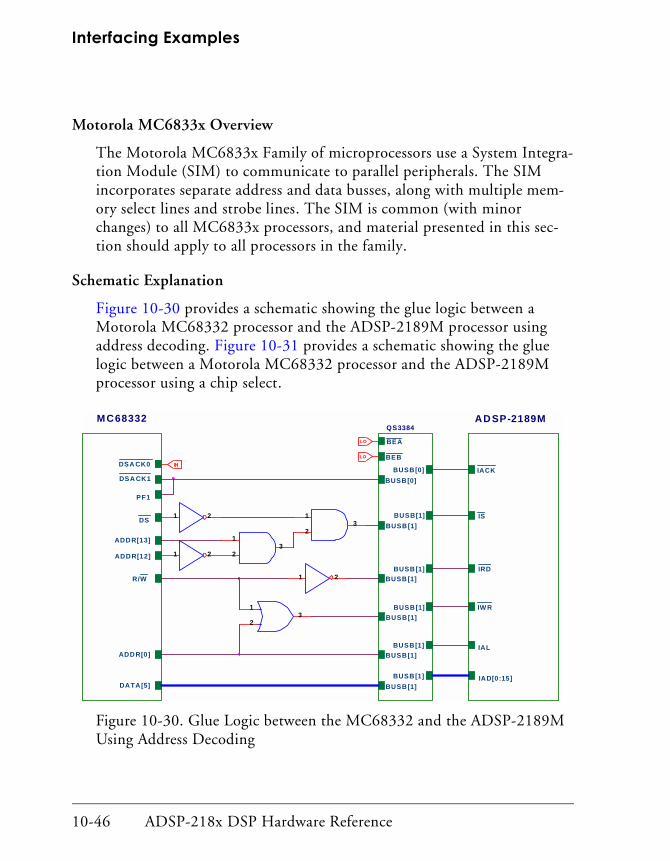
Interfacing Examples
Motorola MC6833x Overview
The Motorola MC6833x Family of microprocessors use a System Integra-tion Module (SIM) to communicate to parallel peripherals. The SIM incorporates separate address and data busses, along with multiple mem-ory select lines and strobe lines. The SIM is common (with minor changes) to all MC6833x processors, and material presented in this sec-tion should apply to all processors in the family.
Schematic Explanation
Figure 10-30 provides a schematic showing the glue logic between a Motorola MC68332 processor and the ADSP-2189M processor using address decoding. Figure 10-31 provides a schematic showing the glue logic between a Motorola MC68332 processor and the ADSP-2189M processor using a chip select.
QS3384
BEA
BEB
BUSB[0]
ADSP-2189M
IAD[0:15]
IACK
IS
IW R
IRD
IAL
MC68332
DS
DSA CK0
PF1
R/W
ADDR[13]
LO
LO
1 2
1 2
1
23
1
23
1 2
1
23
DSA CK1
ADDR[12]
ADDR[0]
DATA[5]
BUSB[0]
BUSB[1]
BUSB[1]
BUSB[1]BUSB[1]
BUSB[1]
BUSB[1]
BUSB[1]
BUSB[1]
BUSB[1]
BUSB[1]
Figure 10-30. Glue Logic between the MC68332 and the ADSP-2189M Using Address Decoding
10-46 ADSP-218x DSP Hardware Reference

Hardware Interfacing and Examples
Minimal logic is required to connect the external bus of the MC6833x to the IDMA port. All logic necessary for this interface is programmed into a single GAL20V8B programmable logic device. The 16 data lines from the MC6833x are connected via a logic level translator to the ADSP-2189’s IAD pins. The MC6833x uses this bus to transmit the DSP memory address, as well as, transfer data to and from the DSP processor.
The IACK signal from the DSP is routed to both the DSACK1 pin and a pro-grammable flag pin on the MC6833x. The DSACK1 pin signals the end of a memory transfer cycle for the MC6833x, while the programmable flag pin is used by the MC6833x to check IACK status prior to initiating a transfer.
LO
LO
U4A
74LS32
1
23
U7A
74LS04
1 2
U9A
74LS32
1
23
MC68332
DS
DSACK0
PF1
R/W
CS7
DSACK1
ADDR[1]
DATA[0:5]
QS3384
BEA
BEB
BUSB[0]
ADSP-2189M
IAD[0:15]
IACK
IS
IW R
IRD
IAL
BUSB[0]
BUSB[1]
BUSB[1]
BUSB[1]
BUSB[1]
BUSB[1]BUSB[1]
BUSB[1]
BUSB[1]
BUSB[1]
BUSB[1]
Figure 10-31. Glue Logic Between the MC68332 and the ADSP-2189M Using a Chip Select
ADSP-218x DSP Hardware Reference 10-47

Interfacing Examples
Listing 10-1 on page 10-55 shows the microcontroller downloader code, which checks for a low level of the flag prior to any transfer.
The microcontroller’s address pin A1 is connected directly to the ALE pin of the IDMA port. To begin a transfer, the microcontroller must first ini-tialize the DSP’s IDMAA register through an address latch cycle. This is accomplished by writing the DSP memory address that the microcontrol-ler wants to access to address 0xbbb2 in the microcontroller’s memory space.
Address pin A1 is used because it is the least significant address pin used by the microcontroller during 16-bit word transfers. You can assign the base address at which the ADSP-2189 IDMA port resides (in the MC6833x's external memory map) in two different ways:
• Using the MC6833x’s address lines A12 and A13 in conjunction with the microcontroller’s DS signal
• Using one of the MC6833x Chip Select pins
These signals (A12, A13, DS, CS7) are logically combined so that the IDMA port's IS signal is asserted (low) when the MC6833x's DS pin is asserted (low), A12 is low and A13 is high. With this combination, the IDMA port can be accessed in the microcontroller’s memory space at addresses 0x2xxx, 0x6xxx, 0xaxxx, and so on. In the example shown in Figure 10-30 on page 10-46, we use address 0x2000 for data transfers and 0x2002 for IDMA address transfers. Tighter assignment of addresses can be accom-plished through the use of additional address lines in the IS logic.
The final IDMA control lines that need to be driven by the MC68332 are IRD (IDMA Read) and IWR (IDMA Write). Since the microcontroller has only a single, multiplexed R/W (Read/Write) line, the R/W line is inverted and then routed to IRD to generate the IDMA read signal. The IDMA write signal, IWR, is the OR’ed combination of the microcontroller’s R/W line, and address line 2. This logic is necessary to insure that IWR stays high during an IDMA address latch cycle.
10-48 ADSP-218x DSP Hardware Reference

Hardware Interfacing and Examples
System Design Issues
The physical hardware interface between the microcontroller and DSP is just the enabling step in a DSP-based co-processing system. System start-up and host-DSP communication issues must be planned for ahead of time and adequate provisions for these issues should be included into both the microcontroller’s and the DSP’s firmware.
Booting the DSP
The IDMA port on the DSP can be used to boot load the DSP on pow-erup. This eliminates the need for a separate EPROM for the DSP. On the ADSP-2189, booting is controlled through the use of the Mode [A,B,C,D] pins. Booting through the IDMA port is enabled by holding the Mode B, D pin low, and the Mode A,C pin high. With this signal combination, upon deassertion of the RESET signal, the DSP does not activate its external address bus to access an EPROM. Instead, the DSP expects a host to begin IDMA transfers to fill its internal Data Memory and Program Memory. This process consists of the host performing standard IDMA instruction and data transfers.
Booting is terminated when the DSP restart vector at DSP Address PM(0x0000) is written. An efficient boot loading sequence would consist of the host filling the DSP’s internal Program Memory, starting at loca-tion PM(0x0001), and using the automatic address increment feature on the IDMA port to speed the transfer of code block in ascending address order. The host can then initialize Data Memory.
ADSP-218x DSP Hardware Reference 10-49

Interfacing Examples
When all initialization is complete, the host should then initialize the DSP’s restart vector. Then, the DSP program execution commences. This booting process is shown in Figure 10-32.
Latch Address(PM(0x0001)
Download FirstPM Segm ent
Download Additio nalPM Segm ents*
Download DMSegments**
Latch Address(PM(0x0000)
DownloadRestart Vector
Each segm ent download requiresits own address latch cycle.
DM segm ents can be downloaded first
or interm ixed between PM segm ents.
*
**
Figure 10-32. IDMA Booting Process
10-50 ADSP-218x DSP Hardware Reference

Hardware Interfacing and Examples
Generating Boot Code
The ADSP-218x processors operate on 24-bit instruction opcodes. The IDMA port can only accept 16-bit values. To transfer instruction opcodes through the IDMA port, the most significant 16 bits are transferred first.
The DSP's IDMA boot files are produced by the ADSP-218x family PROM Splitter, elfspl21.exe. The PROM Splitter command line switch, -idma, is used to generate an ASCII text output file that is suitable for booting an ADSP-2181, ADSP-2183, ADSP-2184, ADSP-2185, or ADSP-2186 processor. An additional command line switch, -218x, enables support for IDMA booting for the ADSP-2187, ADSP-2188, and ADSP-2189 processors, which have additional on-chip memory overlay regions for booting via the IDMA port.
The output file contains a series of IDMA transfer records, each starting with a count (of 16 bit words), an address (consisting of the 14 bit inter-nal address (IDMAA) and the 1 bit IDMAD), to be written to the IDMA Control register. When using the PROM Splitter's -218x command line switch, an additional address word, which represents the IDMA overlay page, is included in the IDMA image file, immediately after the IDMA control word. Each word is expressed as four characters, which represent a 16-bit value in hexadecimal format. The data is displayed as one word per line, as follows:
00A8 <—— count value0001 <—— IDMA control word8000 <—— IDMA OVERLAY control word (218x)0001 <—— First Opcode (16 bit MSB), (count -2)0002 <—— First Opcode (8 bit LSB), (count -3)0001 <—— Second Opcode (16 bit MSB), (count -4)0002 <—— Second Opcode (8 bit LSB), (count -5): :: :: :: :5678 <—— Last Opcode (16 bit MSB), (count =1)
ADSP-218x DSP Hardware Reference 10-51

Interfacing Examples
0090 <—— Last Opcode (8 bit LSB), (count =0): :: : <—— additional PM or DM Segments: :FFFF <—— End-of-module specifier
Host Code Generation Downloading Issues
In order to utilize the data file produced by the PROM Splitter program, the microcontroller needs to be programmed to understand the given for-mat. The PROM Splitter program produces a IDMA image file that can be initialized somewhere in the microcontroller’s memory space. Figure 10-33 shows the format of this image file.
IDMA Word Count
IDM A Starting Address(IDM A Contro l Register)
IDM A Overlay Control Word
IDM A data word 1
IDM A data word 2
.
.
.
IDM A data w ord n
Figure 10-33. IDMA Image File Format
10-52 ADSP-218x DSP Hardware Reference

Hardware Interfacing and Examples
The first element read from the image file is the number of 16-bit words (IDMA Word Count) to be transferred to the DSP (remember that each 24-bit PM opcode counts as two 16-bit words). This value is placed in a data register and can be used as a loop counter to control the download function.
The next value in the IDMA image file is the DSP starting address (IDMA Starting Address), which is the 15-bit value that represents the starting address of the code or data segment that will be transferred during the IDMA access. This starting address value should be written from the host processor into the DSP's IDMA Control register. The DSP's starting address is then followed by the IDMA Overlay Control word, which is used to assign the proper internal DSP overlay memory region that will be accessed during the IDMA transfer.
! Please keep in mind that the IDMA Overlay register applies only for the ADSP-2187, ADSP-2188, and ADSP-2189 processors.
The next values are the data or instruction values (IDMA data word 1…n) that need to be transferred. When the microcontroller has transferred the proper number of items (as determined by the count), it gets the next count value from the buffer, the next DSP address, and so on.
The download process stops when the microcontroller encounters a count value of 0xffff. This download process is shown in Figure 10-34. MC68332 assembly code to implement this download process is presented in Listing 10-1 on page 10-55.
ADSP-218x DSP Hardware Reference 10-53

Interfacing Examples
Done
CountExpired?
Yes
No
Read Count Value
Read DSP StartingAddress
Write DSP StartingAddress to 6833x
Address $4000
Read DSP OverlayControl Word
Write DSP OverlayControl Word to 6833x
Address $4002
Read Data Value fromBuffer and Write to 6833x
Address $4000
Read Next Count or Done
Yes
No Count=FFFF
?
Figure 10-34. MC6833x Download Flow Process
10-54 ADSP-218x DSP Hardware Reference

Hardware Interfacing and Examples
Listing 10-1. Downloading Code and Data to ADSP-2189 IDMA Port Interface Example (MC6833x Assembly Code)
; download.asm;; This code runs on an MC6833x processor and is used to ; download code and data segments to an ADSP-2189 IDMA port ; interface.; Note: The ADSP-2189 is a 3.3V device in order to avoid damage; use 5V to 3.3V logic level Voltage translator (e.g. QS 3384);SCDR EQU $fffc0e ;SCI Data RegisterSCCR0 EQU $fffc08 ;SCI Control Register 0SCCR1 EQU $fffc0a ;SCI Control Register 1QMCR EQU $fffc00 ;QSM Configuration RegisterSCSR EQU $fffc0c ;SCI Status RegisterSRAMBAH EQU $fffb44 ;SRAM Base Address Register High WordSRAMMCR EQU $fffb40 ;SRAM Module Configuration RegisterFYPCR EQU $fffa21 ;SCIM System Protection Control RegisterSIMMCR EQU $fffa00 ;SCIM Configuration RegisterCSPAR0 EQU$fffa44 ;Chip Select Pin Assignment Register 0CSPAR1 EQU $fffa46 ;Chip Select Pin Assignment Register 1CSBAR0 EQU $fffa4c ;Chip Select Base Register 0CSOR0 EQU $fffa4e ;Chip Select Option Register 0PORTF0 EQU $fffa18 ;Port F Data Register
; 6833x MEMORY MAP:
; $000000-$0003FF Interrupt Vector Table TRAM; $000400-$000DFF Code Space TRAM; $010000-$0101FF Variables (left blank) SRAM; $0101FF-Downward Stack Space SRAM; ***********************************************************; Variables; DSP Code and Data will be placed here; ***********************************************************
org $010000
; Opcode and data information for DSP download should be; included here
org $000400
ADSP-218x DSP Hardware Reference 10-55

Interfacing Examples
; ***********************************************************; Init: Beginning of the CODE segment; ***********************************************************
Init:move.b #$0,(FYPCR).L ; Turn off watchdog timermove.l #$101FE,a7 ; Stack at location $101FEmove.w #$0001,(SRAMBAH).L ; Move SRAM to $10000move.w #$0000,(SRAMMCR).L ; Turn on SRAM (Variables/Stack)move.w #$0040,(SIMMCR).L ; Enable User Modemove.w #$3FFF,(CSPAR0).L ; Enable Chip Selects 0-5move.w #$03FF,(CSPAR1).L ; Enable Chip Selects 6-10move.w #$0000,(CSBAR0).L ; Use Chip Select 0move.w #$3822,(CSOR0).L ; Assert Chip Select 0
top:move.w (PORTF0).l,d1 ; Check PF1 to see if IACK low and.w #$0002,d1 ; before proceedingbne topmove.l #$002002,a4 ; initialize a4 with Address
; Latch addressmove.l #$002000,a3 ; initialize a3 with data port
; addressmove.l #$010000,a2 ; initialize a2 to start of DSP
; code/datamove.w (a2)+,d2 ; load count value into d2
tx_rx_loop:
move.w (PORTF0).l,d1 ; check PF1 to see if IACK lowand.w #$0002,d1bne t x_rx_loopmove.w (a2)+,(a4) ; write starting address to IDMAAmove.w (a2)+,(a4) ; write IDMA OVERLAY register
; (218x)sub.w #$1,d2 ; decrement count
tx_dat a:
move.w (a2)+,(a3) ; transfer next instruction
10-56 ADSP-218x DSP Hardware Reference

Hardware Interfacing and Examples
wait_data:move.w (PORTF0).l,d1 ; check PF1 to see if /IACK lowand.w #$0002,d1bne wait_datadbf d2,tx_data ; decrement count to see if at end
; of modulemove (a2),d4 ; get next count valuesub.w #$ffff,d4 ; check if end of all modulesbeq done_data ; if at end, send Restart vector
; if booting, done otherwisemove (a2)+,d2 ; get next module countbra tx_rx_loop ; go back to transferring DSP
; information
done_data:bra done_data ; data file is completed.
Host-DSP Message Transfers
In addition to boot-loading the DSP, many systems require continuous interaction between a host microcontroller and the DSP computation engine. The IDMA port of the ADSP-2189 processor was designed so that there does not need to be any DSP core involvement with host microcon-troller transfers. The host processor is expected to manage the data flow to and from the DSP.
No DSP interrupts are generated during IDMA accesses, and IDMA transfers occur asynchronously to DSP operation. Therefore, the system designer must allocate DSP internal memory resources and arbitrate host accesses so that there is no conflict between host access and DSP access of DSP internal memory resources. For data transfers, one could allocate an area of internal memory for “messages” and constrain the host to access this area only. For code transfers other than booting, a software flag set in this “message” area could be used to signal the host that the DSP is avail-able for transfer.
ADSP-218x DSP Hardware Reference 10-57

Interfacing Examples
Advanced Topics
This section discusses some issues that the system designer may find help-ful when using the Motorola MC68332 for more complex systems.
Multiple Processors
In this hardware example, we focused on connecting a single ADSP-2189M DSP to a Motorola MC68332 microprocessor. This scheme can easily be expanded to support multiple DSP processors, with-out additional glue logic. In a multiple DSP system, multiple IS lines are needed to select each individual DSP processor. The multiple IACK signals from each DSP can be bussed together in a “wired-OR” configuration to create a single IACK signal to the host processor. The 100-pin ADSP-218x processors (all ADSP-218x processors except for the ADSP-2181 and ADSP-2183) support this “wired-OR” IACK logic configuration when their Mode C and Mode D pins are set to a logic high. In this configuration, an external pulldown resistor is needed, since the IACK signal is driven from an open-drain PMOS transistor.
For our system design, each DSP processor requires two of the Motorola 6833x’s memory locations: one memory location is used to perform an IDMA address latch sequence; the other is used for transmitting or receiv-ing IDMA data. Both memory location addresses are used to assert the appropriate IS signal of the specific DSP processor in the system that the host processor wishes to access. In this manner, each DSP processor can be accessed individually.
10-58 ADSP-218x DSP Hardware Reference

Hardware Interfacing and Examples
Hardware Signaling
In many instances, it may be desirable for the host and DSP processors to have additional avenues of communication. The host can use one of its programmable flags as an output attached to a hardware interrupt on the DSP. With this method, the host can alert the DSP before a transfer occurs or inform the DSP that a transfer has been completed. This method can be especially useful since there is no interrupt associated with IDMA operation on the ADSP-2189. The DSP can likewise use a pro-grammable flag as an output to signal the host if there is new data for the host to use or if new code is required for download.
ReferencesThe following is a list of references for materials used in developing this chapter and for materials that provide additional information. Please note that many of these materials can be found on Analog Devices’ Web pages at www.analog.com.
• Steven W. Smith, The Scientist and Engineer’s Guide to Digital Signal Processing, Second Edition, 1999, California Technical Publishing, P.O. Box 50240, San Diego, CA 92150.
• C. Britton Rorabaugh, DSP Primer, McGraw-Hill, 1999.
• Richard J. Higgins, Digital Signal Processing in VLSI, Pren-tice-Hall,1990.
• DSP Designer’s Reference (DSP Solutions) CDROM, Analog Devices,1999.
• DSP Navigators: Interactive Tutorials about Analog Devices’ DSP Architectures (ADSP-218x family):
• DSP Training and Workshops:
ADSP-218x DSP Hardware Reference 10-59

References
• ADSP-2100 Family EZ-KIT Lite Reference Manual.
• ADSP-2100 Family DSP Applications, Vol. 1 and Vol. 2.
• M68300 Family CPU32 Reference Manual, Motorola, Inc. (refer-ence number CPU32RM/AD)
• Modular Microcontroller Family SIM Reference Manual, Motorola, Inc. (reference number SIMRM/AD)
• MC68F333 User’s Manual, Motorola, Inc. (reference number MC68F333UM/AD)
• 68F333 Development Kit User’s Manual, Revision 1.00, P&E Micro-computer Systems, Inc.
10-60 ADSP-218x DSP Hardware Reference

A NUMERIC FORMATSFigure A-0.
Table A-0.
Listing A-0.
OverviewADSP-218x family processors support 16-bit fixed-point data in hard-ware. Special features in the computation units allow you to support other formats in software. This appendix describes various aspects of the 16-bit data format. It also describes how to implement a block floating-point for-mat in software.
Unsigned or Signed: Twos-Complement Format
Unsigned binary numbers may be thought of as positive, having nearly twice the magnitude of a signed number of the same length. The least sig-nificant words of multiple precision numbers are treated as unsigned numbers.
Signed numbers supported by the ADSP-218x family are in twos-comple-ment format. Signed-magnitude, ones-complement, BCD or excess-n formats are not supported.
ADSP-218x DSP Hardware Reference A-1

Integer or Fractional Format
Integer or Fractional FormatThe ADSP-218x family supports both fractional and integer data formats, with the exception that the ADSP-2100 processor does not perform inte-ger multiplication. In an integer, the radix point is assumed to lie to the right of the LSB, so that all magnitude bits have a weight of 1 or greater. This format is shown in Figure A-1, which can be found on the following page. Note that in twos-complement format, the sign bit has a negative weight.
In a fractional format, the assumed radix point lies within the number, so that some or all of the magnitude bits have a weight of less than 1. In the format shown in Figure A-2, the assumed radix point lies to the left of the 3 LSBs, and the bits have the weights indicated.
15 14 13
• • •
2 1 0
–(2 ) 2 2 2 2 215 14 13 2 1 0
SignBit
Weight
Bit
Signed Integer
15 14 13
• • •
2 1 0
2 2 2 2 2 215 14 13 2 1 0
Weight
Bit
Unsigned Integer
RadixPoint
RadixPoint
Figure A-1. Integer Format
A-2 ADSP-218x DSP Hardware Reference

Numeric Formats
The notation used to describe a format consists two numbers separated by a period (.); the first number is the number of bits to the left of radix point, the second is the number of bits to the right of the radix point. For example, 16.0 format is an integer format; all bits lie to the left of the radix point. The format shown in Figure A-2 is 13.3.
15 14 13
• • •
2 1 0
–(2 ) 2 2 2 2 212 11 10 –1 –2 –3
SignBit
Weight
Bit
Signed Fractional (13.3)
15 14 13
• • •
2 1 0
2 2 2 2 2 212 11 10 –1 –2 –3
Weight
Bit
Unsigned Fractional (13.3)
4 3
2 21 0
4 3
2 21 0
RadixPoint
RadixPoint
Figure A-2. Fractional Format
ADSP-218x DSP Hardware Reference A-3

Integer or Fractional Format
Table A-1 shows the ranges of numbers that can be represented in the fractional formats that are possible with 16 bits.
Table A-1. Fractional Formats and Their Ranges
Format # of Integer Bits
# of Fractional Bits
Max Positive Value (0x7FFF) In Decimal
Max Negative Value (0x8000) In Decimal
Value of 1 LSB (0x0001) In Decimal
1.15 1 15 0.999969482421875 –1.0 0.000030517578125
2.14 2 14 1.999938964843750 –2.0 0.000061035156250
3.13 3 13 3.999877929687500 –4.0 0.000122070312500
4.12 4 12 7.999755859375000 –8.0 0.000244140625000
5.11 5 11 15.999511718750000 –16.0 0.000488281250000
6.10 6 10 31.999023437500000 –32.0 0.000976562500000
7.9 7 9 63.998046875000000 –64.0 0.001953125000000
8.8 8 8 127.996093750000000 –128.0 0.003906250000000
9.7 9 7 255.992187500000000 –256.0 0.007812500000000
10.6 10 6 511.984375000000000 –512.0 0.015625000000000
11.5 11 5 1023.968750000000000 –1024.0 0.031250000000000
12.4 12 4 2047.937500000000000 –2048.0 0.062500000000000
13.3 13 3 4095.875000000000000 –4096.0 0.125000000000000
14.2 14 2 8191.750000000000000 –8192.0 0.250000000000000
15.1 15 1 16383.500000000000000 –16384.0 0.500000000000000
16.0 16 0 32767.000000000000000 –32768.0 1.000000000000000
A-4 ADSP-218x DSP Hardware Reference

Numeric Formats
Binary MultiplicationIn addition and subtraction, both operands must be in the same format (signed or unsigned, radix point in the same location) and the result for-mat is the same as the input format. Addition and subtraction are performed the same way whether the inputs are signed or unsigned.
In multiplication, however, the inputs can have different formats, and the result depends on their formats. The ADSP-218x family assembly lan-guage allows you to specify whether the inputs are both signed, both unsigned, or one of each (mixed-mode). The location of the radix point in the result can be derived from its location in each of the inputs. This is shown in Figure A-3. The product of two 16-bit numbers is a 32-bit num-ber. If the inputs’ formats are M.N and P.Q, the product has the format (M+P).(N+Q). For example, the product of two 13.3 numbers is a 26.6 number. The product of two 1.15 numbers is a 2.30 number.
16-Bit Examples:
5.35.3
10.6
1.15
1.15
2.30
1.111
11.11
1
1
1
1
1
1
1
1
1
1
1
1
1
1
1
1
0 1001
1.3 format
2.2 format
3.5 format = (1+2) . (2+3)
4-Bit Example:
M.N
P.Q
(M+P) . (N+Q)
General Rule:
011.
Figure A-3. Format of Multiplier Result
ADSP-218x DSP Hardware Reference A-5

Binary Multiplication
Fractional Mode and Integer ModeA product of 2 twos-complement numbers has two sign bits. Since one of these bits is redundant, you can shift the entire result left one bit. Addi-tionally, if one of the inputs was a 1.15 number, the left shift causes the result to have the same format as the other input (with 16 bits of addi-tional precision). For example, multiplying a 1.15 number by a 5.11 number yields a 6.26 number. When shifted left one bit, the result is a 5.27 number, or a 5.11 number plus 16 LSBs.
The ADSP-218x family provides a mode (called the fractional mode) in which the multiplier result is always shifted left one bit before being writ-ten to the result register. This left shift eliminates the extra sign bit when both operands are signed, yielding a correctly formatted result.
When both operands are in 1.15 format, the result is 2.30 (30 fractional bits). A left shift causes the multiplier result to be 1.31 which can be rounded to 1.15. Thus, if you use a fractional data format, it is most con-venient to use the 1.15 format.
In the integer mode, the left shift does not occur. This is the mode to use if both operands are integers (in the 16.0 format). The 32-bit multiplier result is in 32.0 format, also an integer.
In all ADSP-218x DSPs, fractional and integer modes are controlled by a bit in the MSTAT register. At reset, these processors default to the fractional mode.
A-6 ADSP-218x DSP Hardware Reference

Numeric Formats
Block Floating-Point FormatA block floating-point format enables a fixed-point processor to gain some of the increased dynamic range of a floating-point format without the overhead needed to do floating-point arithmetic. However, some addi-tional programming is required to maintain a block floating-point format.
A floating-point number has an exponent that indicates the position of the radix point in the actual value. In block floating-point format, a set (block) of data values share a common exponent. To convert a block of fixed-point values to block floating-point format, you would shift each value left by the same amount and store the shift value as the block exponent.
Typically, block floating-point format allows you to shift out non-signifi-cant MSBs, increasing the precision available in each value. You can also use block floating-point format to eliminate the possibility of a data value overflowing. Figure A-4 shows an example.
0x0FFF
0x1FFF
0x07FF
=
=
=
0000
0001
0000
1111
1111
0111
1111
1111
1111
1111
1111
1111
2 Guard Bits
Sign Bit
To detect bit growth into 2 guard bits, set SB=–2
Figure A-4. Data With Guard Bits
ADSP-218x DSP Hardware Reference A-7

Block Floating-Point Format
The three data samples each have at least 2 non-significant, redundant sign bits. Each data value can grow by these two bits (two orders of magni-tude) before overflowing; thus, these bits are called guard bits. If it is known that a process will not cause any value to grow by more than these two bits, then the process can be run without loss of data. Afterward, how-ever, the block must be adjusted to replace the guard bits before the next process.
Figure A-5 shows the data after processing but before adjustment.
0x1FFF
0x3FFF
0x07FF
=
=
=
0001
0011
0000
1111
1111
0111
1111
1111
1111
1111
1111
1111
1 Guard Bit
Sign Bit
EXPADJ instruction checks exponent, adjusts SB
Exponent = –2
Exponent = –1
Exponent = –4
SB = –2
SB = –1
SB = –1
0x0FFF
0x1FFF
0x03FF
=
=
=
0000
0001
0000
1111
1111
0011
1111
1111
1111
1111
1111
1111
2 Guard Bits
Sign Bit
1. Check for Bit Growth
2. Shift Right to Restore Guard Bits
Figure A-5. Block Floating-Point Adjustment
A-8 ADSP-218x DSP Hardware Reference

Numeric Formats
The block floating-point adjustment is performed as follows. Initially, the value of SB is –2, corresponding to the 2 guard bits. During processing, each resulting data value is inspected by the EXPADJ instruction, which counts the number of redundant sign bits and adjusts SB is if the number of redundant sign bits is less than 2. In this example, SB=–1 after process-ing, indicating that the block of data must be shifted right one bit to maintain the 2 guard bits. If SB were 0 after processing, the block would have to be shifted two bits right. In either case, the block exponent is updated to reflect the shift.
ADSP-218x DSP Hardware Reference A-9

Block Floating-Point Format
A-10 ADSP-218x DSP Hardware Reference

B CONTROL/STATUS REGISTERS
Figure B-0.
Table B-0.
Listing B-0.
OverviewThis appendix shows bit definitions for ADSP-218x memory-mapped control registers and non-memory-mapped control and status registers. The memory-mapped registers are listed in descending address order. Default bit values at reset are shown. If no value is shown, the bit is unde-fined at reset. Reserved bits are shown on a grey field. These reserved bits must be set to zero.
ADSP-218x DSP Hardware Reference B-1
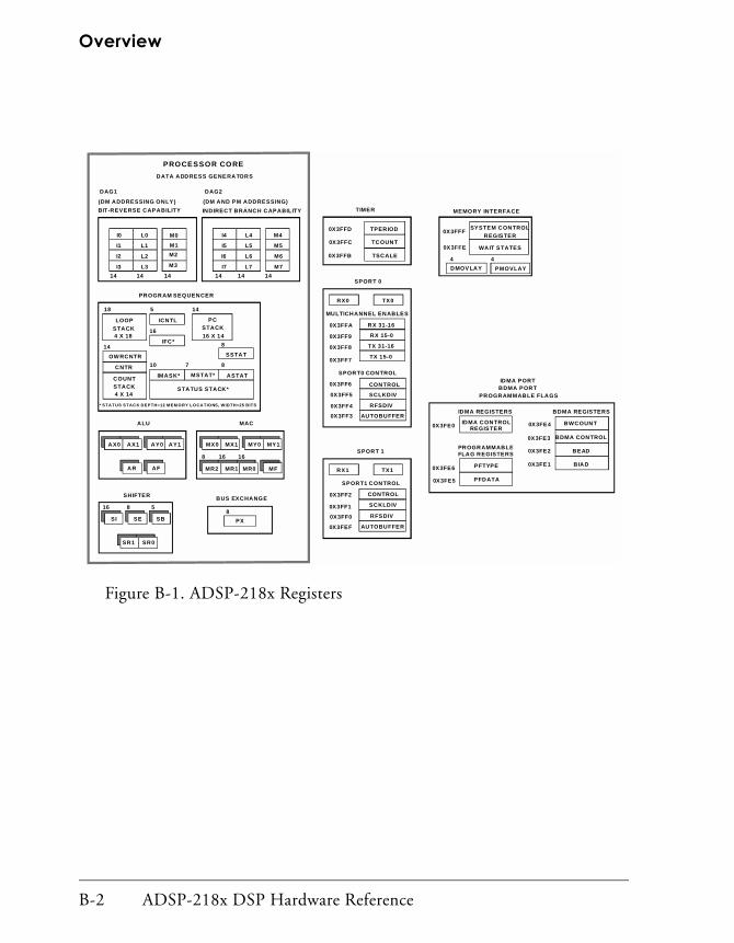
Overview
RFSDIV
SCLKDIV
ALU MAC
SHIFTER
PROGRAM SEQUENCER
I3
I0
I1
I2
L0
L1
L2
L3
CNTR
OW RCNTR
PX
COUNT STACK4 X 14
ASTAT
STATUS STACK*
MSTAT*IMASK*
PC STACK16 X 14
LOOP STACK4 X 18
IFC*
ICNTL
SSTAT
AX0 AX1 AY1AY0
AFAR
MX0 MX1 MY1MY0
MR0MR1MR2 MF
SR0SR1
SI SE SB
M0
M1
14 1414
M3
14 1414
M5
M6
M7I7
I4
I5
I6
L5
L6
L7
M4L4
14
18 14
58
8
8
8
BUS EXCHANGE
5
8 16 16
* STATUS STAC K DEPTH=12 MEM ORY LOCA TIONS, WIDTH=25 BITS
DATA ADDRESS GENE RATORS
(DM ADDRESSING ONLY) (DM AND PM ADDRESSING)
BIT-REVERSE CAPABILITY INDIRECT BRANCH CAPABILITY
DAG1 DAG2
SPORT 0
RX0 TX0
SPORT0 CONTROL
0X3FFA
0X3FF9
0X3FF8
0X3FF7
MULTICHANNEL ENABLES
RX 31-16
RX 15-0
TX 31-16
TX 15-0
AUTOBUFFER
0X3FF6
0X3FF5
0X3FF4
0X3FF3
CONTROL
RX1 TX1
SPORT 1
SPORT1 CONTROL
0X3FF2
0X3FF1
0X3FF0
0X3FEF
TIMER
TPERIOD
TCOUNT
0X3FFD
0X3FFC
0X3FFB
BDMA PORTPROGRAMMABLE FLAGS
0X3FE0 BWCOUNT
BDMA CONTROL
BEAD
0X3FE4
0X3FE3
0X3FE2
BIAD0X3FE1
IDMA CONTROL REGISTER
BDMA REGISTERS
0X3FE6 PFTYPE
0X3FE5 PFDATA
IDMA REGISTERS
PROGRAMMABLEFLAG REGISTERS
IDMA PORT
MEMORY INTERFACE
0X3FFF
0X3FFE WAIT S TATES
PMOVLAY
4
DMOV LAY
4
PROCESSOR CORE
M2 TSCALE
SYSTEM CONTROLREGISTER
AUTOBUFFER
CONTROL
SCKLDIV
RFSDIV
16
10 7
16
Figure B-1. ADSP-218x Registers
B-2 ADSP-218x DSP Hardware Reference

Control/Status Registers
Memory-Mapped Registers
PWAIT
BMS Disable *
SPORT0 Enable
1 = enabled, 0 = disabled
SPORT1 Enable
1 = enabled, 0 = d isabled
SPORT1 Configure
1 = Serial Port0 = FI, FO, IRQ0, IRQ1, SCLK
System Control
DM(0x3FFF)
Note: Reserved bits15-13 and 9-4must always be set to 0.
*
15 14 13 12 11 10 9 8 7 6 5 4 3 2 1 0
00 0 0 0 0 1 0 0 0 0 0 0
PR OG RA M MEM O RY
The BMS Disable bit applies toall L, M, and N series processors andthe ADSP-2184 and ADSP-2186processors. This bit is unused in allother ADSP-218x processors andshould be set to 0.
0 = enabled, 1= disabled
11 1
Figure B-2. System Control Register
Default bit va lues at reset are shown. If no va lue is shown, the bit is undefined at reset.Reserved bits are shown on a grey field . These reserved bits must be set to zero.
ADSP-218x DSP Hardware Reference B-3

Memory-Mapped Registers
IOWAIT0IOWAIT1IOWAIT2IOWAIT3DWAIT
DM(0x3FFE )
Wait State Mode Select0 = norm al mode (PWAIT, DWAIT, IOWAIT0-3 = N wait states, ranging from 0 to 7)1= 2N+1 mode (PW AIT, D WAIT, IOWAIT0-3 = 2N+1 wait states, ranging from 0 to 15)
W ait State Control
15 14 13 12 11 10 9 8 7 6 5 4 3 2 1 0
1
(ADSP-218x M and N Series Processors )
1 1 1 1 1 1 1 1 1 1 11 1 1 1
Figure B-3. Wait State Control Register (ADSP-218x M and N Series)
(All ADSP-218x P rocessors except ADSP-218x M an d N Series)
IOWAIT0IOWAIT1IOWAIT2IOWAIT3DWAIT
DM(0x3FFE )
Wait State Control
15 14 13 12 11 10 9 8 7 6 5 4 3 2 1 0
0 1 1 1 1 1 1 1 1 1 1 11 1 1 1
Figure B-4. Wait State Control Register (All ADSP-218x Processors exceptthe M and N Series)
Default bit va lues at reset are shown. If no va lue is shown, the bit is undefined at reset.Reserved bits are shown on a grey field . These reserved bits must be set to zero.
B-4 ADSP-218x DSP Hardware Reference

Control/Status Registers
1 5 1 4 1 3 1 2 1 1 1 0
TPERIOD Period Register
TCOUNT Counter Register
TSCALE S caling Register00000000
Tim er
DM(0x3FFC)
DM(0x3FFB)
DM(0x3FFD)
9 8 7 6 5 4 3 2 1 0
Figure B-5. Timer Registers
DM(0x3FF6)
15 14 13 12 11 10
M CEM ultichannel Enable
ISCLKInternal Serial Clock Generation
RFSRReceive Frame Sync Required
TFSRTransm it Frame Sync Required
TFSWTransm it Frame Sync Width
RFSWReceive Frame Sync Width
M FDM ultichannel Fram e Delay
IRFSInternal Receive Frame Sync Enable
INVTFSInvert Transm it Fram e Sync(or INVTDV Invert Transm it Data Valid)
INVRFSInvert Receive Fram e Sync
SLEN (Serial Word Length – 1)
DTYPE Data Form at00=right justify, zero-fill unused M SBs01=right justify, sign-extend into unused MSBs10=compand using µµµµ -law 11=compand using A-law
ITFSInternal Transmit Frame Sync Enable
(or M CL M ultichannel Length:1=32 words, 0=24 words)
(only If Multichannel M ode Enabled )
0000000000000000
(only If M ultichannel Mode Enabled)
(only If M ultichannel Mode Enabled)
SPORT0 Control
9 8 7 6 5 4 3 2 1 0
Figure B-6. SPORT0 Control Register
Default bit va lues at reset are shown. If no va lue is shown, the bit is undefined at reset.Reserved bits are shown on a grey field . These reserved bits must be set to zero.
ADSP-218x DSP Hardware Reference B-5

Memory-Mapped Registers
31 30 29 28 27 26 25 24 23 22 21 20 19 18 17 16
15 14 13 12 11 10 9
31 30 29 28 27 26 25 24 23 22 21 20 19 18 17 16
R eceiv e
W ordEnables
Transm it
W ord
Enables
D M (0x3FFA)
D M (0x3FF9)
D M (0x3FF8)
D M (0x3FF7)
1 = channe l enab led
0 = channe l ignored
S P O R T0 M ultic hanne l W ord E nable
8 7 6 5 4 3 2 1 0
9 8 7 6 5 4 3 2 1 015 14 13 12 11 10
Figure B-7. SPORT0 Multichannel Word Enable Registers
Default bit va lues at reset are shown. If no va lue is shown, the bit is undefined at reset.Reserved bits are shown on a grey field . These reserved bits must be set to zero.
B-6 ADSP-218x DSP Hardware Reference

Control/Status Registers
SPORT0 A utobuffer Control
DM(0x3FF3)
TBUFTransmit Autobuffering Enable
RBUFReceive Autobuffering Enable
TIREG TMREG RIREG RMREG
BIASRNDMAC Biased Ro unding Control Bit
CLKODISCLKOUT Disable Control Bit
0 0 0 0 00
15 14 13 12 11 10 9 8 7 6 5 4 3 2 1 0
0 0 0 0 0 00 0 0 0
Figure B-8. SPORT0 Autobuffer Control Register
SPORT0 SCLKDIV
Serial Clock Divide Modulus
1 5 1 4 1 3 1 2 1 1 10
1 5 1 4 1 3 1 2 1 1 1 0
SPORT0 RFSDIVReceive Frame Sync Divide Modulus
DM(0x3FF4)
DM(0x3FF5)
SCLKfrequ ency
RFS frequency RFSDIV = – 1SCLKDIV =
CLKOUT frequency
2 * (SCLK frequency)
9 8 7 6 5 4 3 2 1 0
9 8 7 6 5 4 3 2 1 0
– 1
Figure B-9. SPORT0 SCLKDIV and RFSDIV Registers
Default bit va lues at reset are shown. If no va lue is shown, the bit is undefined at reset.Reserved bits are shown on a grey field . These reserved bits must be set to zero.
ADSP-218x DSP Hardware Reference B-7

Memory-Mapped Registers
Flag Out (read-only)
15 14 13 12 11 10
ISCLKInternal Serial Clock Generation
RFSR
TFSRTransm it Fram e Sync Required
TFSWTransm it Fram e Sync Width
RFSWReceive Fram e Sync Width
IRFSInternal Receive Fram e Sync Enable
INVTFSInvert Transm it Fram e Sync
INVRFSInvert Receive Fram e Sync
SLEN (Serial Word Length – 1)
DTYPE Data Format
00=right justify, zero-fill unused MSBs
10=com pand using µµµµ -law 11=com pand using A-law
ITFSInternal Transm it Frame Sync Enable
000000000 DM(0x3FF2)
SPORT1 Control
9 8 7 6 5 4 3 2 1 0
00=right justify, sign-extend into unused M SBsReceive Fram e Sync Required
000000
Figure B-10. SPORT1 Control register
Default bit va lues at reset are shown. If no va lue is shown, the bit is undefined at reset.Reserved bits are shown on a grey field . These reserved bits must be set to zero.
B-8 ADSP-218x DSP Hardware Reference

Control/Status Registers
S P O R T1 S C LK D IVS eria l C lock D iv ide M odulus
1 5 1 4 1 3 1 2 1 1 10
1 5 1 4 1 3 1 2 1 1 1 0
S P O R T1 R FS D IVR eceive Fram e Sync D iv ide M odulus
D M (0x3FF0)
D M (0x3FF1)
SC LK freq uency
R FS frequ ency R FSD IV = – 1SC LK DIV =
C LKO U T freq uency
2 * (SC LK freq uency)
9 8 7 6 5 4 3 2 1 0
9 8 7 6 5 4 3 2 1 0
– 1
Figure B-11. SPORT1 SCLKDIV and RFSDIV Registers
Default bit va lues at reset are shown. If no va lue is shown, the bit is undefined at reset.Reserved bits are shown on a grey field . These reserved bits must be set to zero.
ADSP-218x DSP Hardware Reference B-9

Memory-Mapped Registers
SPORT1 Autobuffer Control
15 14 13 12 11 10
TBUFTransmit Autobuffer Enable
RBUFReceive Autobuffer Enable
RMREGReceive M Register
RIREGReceive I Register
TMREGTransmit M Register
TIREGTransmit I Register
XTALDISXTAL pin disable during powerdown
1=disabled, 0=enabled(XTAL pin should be disabled when
no external crystal is connected)
XTALDELAY1=delay, 0=no delay
(Use delay to allow internal phase
oscillator to stabilize)
PDFORCEPowerdown Force
1=force processor to vector to powerdown interrupt
PUCRPowerup Context Reset
1=soft reset (clear context) 0=resume execution
DM(0x3FEF)
9 8 7 6 5 4 3 2 1 0
000 0 00
locked loop or external
Figure B-12. SPORT1 Autobuffer Control Register
Default bit va lues at reset are shown. If no va lue is shown, the bit is undefined at reset.Reserved bits are shown on a grey field . These reserved bits must be set to zero.
B-10 ADSP-218x DSP Hardware Reference
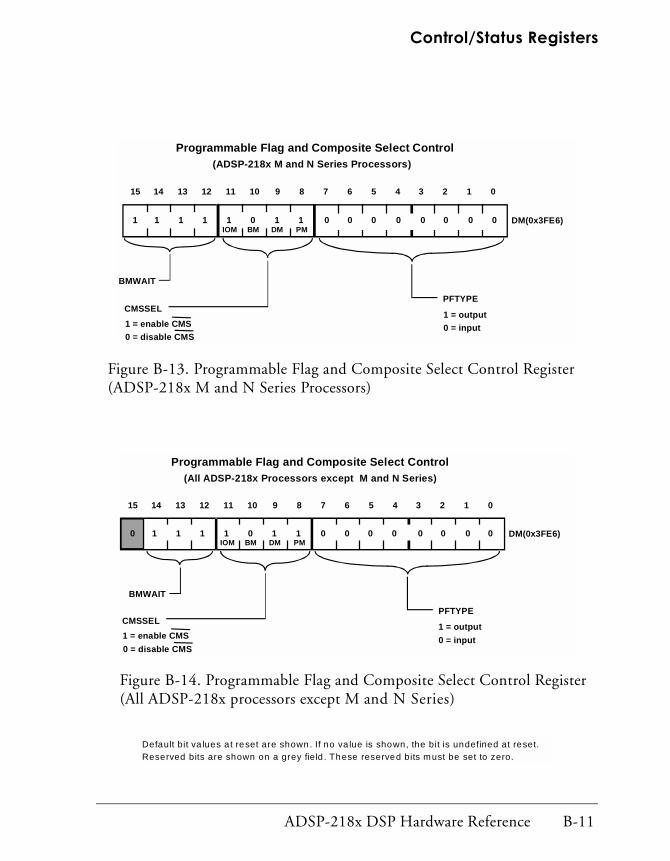
Control/Status Registers
1 = enable CMS
BMWAIT
Programmable Flag and Composite Select Control
CMSSEL
0 = disable CMS
DM(0x3FE6)
15 14 13 12 11 10 9 8 7 6 5 4 3 2 1 0
(ADSP-218x M and N Series Processors)
1 0 1 1DMBMIOM PM
1 1 1 1
PFTYPE
1 = output
0 = input
0 0 0 0 0 00 0
Figure B-13. Programmable Flag and Composite Select Control Register (ADSP-218x M and N Series Processors)
Default bit va lues at reset are shown. If no va lue is shown, the bit is undefined at reset.Reserved bits are shown on a grey field . These reserved bits must be set to zero.
1 = enable CMS
BMWAIT
Programmable Flag and Composite Select Control
CMSSEL
0 = disable CMS
DM(0x3FE6)
15 14 13 12 11 10 9 8 7 6 5 4 3 2 1 0
0
(All ADSP-218x Processors except M and N Series)
1 0 1 1DMBMIOM PM
1 1 1
PFTYPE
0 0 0 0 0 0 0 0
1 = output
0 = input
Figure B-14. Programmable Flag and Composite Select Control Register (All ADSP-218x processors except M and N Series)
ADSP-218x DSP Hardware Reference B-11

Memory-Mapped Registers
PFDATA
Programmable Flag Data
DM(0x3FE5)
15 14 13 12 11 10 9 8 7 6 5 4 3 2 1 0
0 0 0 0 0 0 0 0
Note: At reset the programmable flag pins PF7-PF0are inputs. Therefore, the value of the PFDATA bitfield is determined by the pin inputs (externallydriven) at reset.
Figure B-15. Programmable Flag Data Register
15 1 4 13 12 11 10 9 7 5 3 1
BMPAG E
BDMA Control
DM(0x3FE3)
BDIR
0 = load from BM1 = store to BM
BCR
0 = run during BDM A 1 = halt during BDMA,
Context Reset when done
BTYPE (See table)
BTYPE 00 01 10 11
Internal M emory Space PM D M DM DM
Word Size 24 16 8 8
Alignment Full Full MSB LSB word word
8 6 4 2 0
BMOVLAY
(ADSP-2187 , ADSP-2188, and ADSP-2189)
Figure B-16. BDMA Control Register (All ADSP-2187, ADSP-2188, ADSP-2189 Processors)
Default bit va lues at reset are shown. If no va lue is shown, the bit is undefined at reset.Reserved bits are shown on a grey field . These reserved bits must be set to zero.
B-12 ADSP-218x DSP Hardware Reference

Control/Status Registers
15 1 4 13 12 11 10 9 7 5 3 1
BMPAG E
BDMA Control
DM(0x3FE3)
BDIR
0 = load from BM1 = store to BM
BCR
0 = run during BDM A 1 = halt during BDMA,
Context Reset when done
BTYPE (See table)
BTYPE 00 01 10 11
Internal M emory Space PM D M DM DM
Word Size 24 16 8 8
Alignment Full Full MSB LSB word word
8 6 4 2 0
(All ADSP-218x Processors except ADSP-2187, ADSP-2188, and ADSP-2189 )
Figure B-17. BDMA Control Register (All ADSP-218x Processors except ADSP-2187, ADSP-2188, and ADSP-2189)
Default bit va lues at reset are shown. If no va lue is shown, the bit is undefined at reset.Reserved bits are shown on a grey field . These reserved bits must be set to zero.
ADSP-218x DSP Hardware Reference B-13

Memory-Mapped Registers
00
1 5 1 4 1 3 1 2 1 1 1 0 9 8 7 6 5 4 3 2 1 0
D M (0 x 3 F E 4 )
B D M A W o rd C o u n t
M M A P = 0 a n d B M O D E = 0 (A D S P -2 1 8 1 a n d A D S P -2 1 8 3 o n ly )
B W C O U N T
B W C O U N T
o r
D M (0 x 3 F E 4 )
M O D E B = 0 (A ll o th e r A D S P -2 1 8 x p ro c e s s o rs )
M M A P = 1 o r B M O D E = 1 (A D S P -2 1 8 1 a n d A D S P -2 1 8 3 o n ly )
M O D E B = 1 (A ll o th e r A D S P -2 1 8 x p ro c e s s o rs )
N o te : B its 1 4 a n d 1 5 a re u n u s e da n d s h o u ld b e s e t to 0 .
00
1 5 1 4 1 3 1 2 1 1 1 0 9 8 7 6 5 4 3 2 1 0
0 0 0 0 0 0 0 0 0 00 0 0 0
0 0 0 0 0 0 0 0 0 00 0 1 0
Figure B-18. BDMA Word Count Register
Default bit va lues at reset are shown. If no va lue is shown, the bit is undefined at reset.Reserved bits are shown on a grey field . These reserved bits must be set to zero.
B-14 ADSP-218x DSP Hardware Reference

Control/Status Registers
15 14 13 12 11 10 9 8 7 6 5 4 3 2 1 0
00
B D M A E x te rn a l A dd res s
D M (0x 3F E 2)
B E A D
N o te : B its 14 a n d 15 a re u n u s edan d s h o u ld b e se t to 0 .
0 00 0 0 0 0 0 0 0 0 0 0 0
Figure B-19. BDMA External Address Register
1 5 1 4 1 3 1 2 1 1 1 0 9 8 7 6 5 4 3 2 1 0
00
B D M A In te rn a l A d d re s s
D M (0x 3 F E 1 )
B IA D
N o te : B its 1 4 a n d 1 5 a re u n u s e da n d sh o u ld b e s e t to 0 .
0 00 0 0 0 0 0 0 0 0 0 0 0
Figure B-20. BDMA Internal Address Register
Default bit va lues at reset are shown. If no va lue is shown, the bit is undefined at reset.Reserved bits are shown on a grey field . These reserved bits must be set to zero.
ADSP-218x DSP Hardware Reference B-15

Memory-Mapped Registers
ID M A C ontro l
D M (0x3FE 0)
ID M A A
S tarting a ddress
ID M A D
D estination m em ory type:
0=P M1=D M
N ote: B it 1 5 is a rese rved b it a ndshould b e s et to 0 in a ll A D S P -218xprocesso rs except the A D S P -2187 ,A D S P -218 8 , and A D S P -21 89 .
15 14 13 12 11 10 9 8 7 6 5 4 3 2 1 0
0
Figure B-21. IDMA Control Register
1 5 1 4 1 3 1 2 1 1 1 0 9 8 7 6 5 4 3 2 1 0
ID M A O v e rla y
D M (0 x 3 F E 7 )
ID P M O V L A Y
ID D M O V L A Y
R e s e rv e d
S e t t o 0
N o te 1 : T h e ID D M O V L A Y a n d ID P M O V L A Y b it fiel d s a ppl y onl y t o t h e A D S P -2 1 8 7 , A D S P -
2 1 8 8 , a n d A D S P -2 1 8 9 p ro c e s s o rs . F o r a ll o th e r A D S P -2 1 8 x p ro c e s s o rs , th e s e b its a re
u n u s e d a n d m u s t b e s e t t o 0 .
N o te 2 : T h e s h o r t re a d o n ly b it ( bi t 1 4 ) a p p lie s to M a n d N s e r ie s o n ly .
F o r a ll o th e r A D S P -2 1 8 x p ro c e s s o rs , th is b it is u n u s e d a n d m u s t b e s e t t o z er o.
0 0 0 0 0 0 0 00 0 0 0 0 00 0
R e s e rv e d
S e t t o 0
S h o rt R e a d O n ly
0 = D is a b le , 1 = E n a b le
Figure B-22. IDMA Overlay Register
Default bit va lues at reset are shown. If no va lue is shown, the bit is undefined at reset.Reserved bits are shown on a grey field . These reserved bits must be set to zero.
B-16 ADSP-218x DSP Hardware Reference

Control/Status Registers
Non-Memory Mapped Registers
ASTAT
PC S tack E mpty
PC Stack O verflow
Cou nt S tack Empty
Cou nt Stack O verflow
Status S tack Empty
Statu s Stack O verflow
Loop S tack Empty
Loop Stack O verflow
01234567
10101010
ALU R esult Zero
ALU R esult Negative
ALU Overflow
ALU C arry
ALU X Input S ign
ALU Qu otient
MAC O verflow
Shifter Input Sign
01234567
0000000
SS M V AQ AS AC AV AN AZ
SSTAT (read-only)
0
Figure B-23. ASTAT and SSTAT Registers
Register B ank Select0=prim ary, 1=secon dary
B it-R evers e Addressing Enable (D AG1)
ALU O verflow Latch M od e Enable
AR Saturation M ode Enab le
MA C Resu lt P lacem ent0=fract iona l, 1=integ er
Timer En able
G o M ode Enable
0123456
0000000
Interrupt N estin g
1=edge
0=level
1=enab le0=disab le
IRQ 0 Sens itivity
IRQ 1 Sens itivity
IRQ 2 Sens itivity
MSTAT ICNTL
01234
Figure B-24. MSTAT and ICNTL Registers
Default bit va lues at reset are shown. If no va lue is shown, the bit is undefined at reset.Reserved bits are shown on a grey field . These reserved bits must be set to zero.
ADSP-218x DSP Hardware Reference B-17

Non-Memory Mapped Registers
IMASK
00000000
SP OR T0 R eceive
IRQ L0
IRQ L1
SPO RT0 Transm it
00
BDM A Interrupt
IRQ E
Timer
SPO RT1 Transmit or IRQ 1
INTER RUPT ENA BLES
1 = enable
0 = disable (mask)
9 8 7 6 5 4 3 2 1 0
IRQ 2
SPO RT1 Receive or IR Q0
Figure B-25. IMASK Register
IFC(write-only)
11 10 9
Timer
000000000000
IRQ 2
15 14 13 12
0000
Timer
SPO RT1 Transmit or IRQ 1
SPO RT1 Receive or IR Q0
SPO RT1 Receive or IR Q0
SPO RT1 Transmit or IRQ 1
IRQ 2
BDM A Interrupt
Interrupt Force Bits Interrupt C lear Bits
SPOR T0 R eceive
SPO RT0 Transm it
SP OR T0 R eceive
SPO RT0 Transm it
IRQEBDM A Interrupt
IRQ E
8 7 6 5 4 3 2 1 0
Figure B-26. IFC Register
Default bit va lues at reset are shown. If no va lue is shown, the bit is undefined at reset.Reserved bits are shown on a grey field . These reserved bits must be set to zero.
B-18 ADSP-218x DSP Hardware Reference

C ADVANCED PRODUCT FEATURES
Figure C-0.
Table C-0.
Listing C-0.
OverviewThis appendix provides a summary of advanced features that are included in the ADSP-218x family processors. Table C-1 lists each processor and identifies the features each contains. (For basic features, see Table 1-1 in Chapter 1, “Introduction.”)
Table C-1. ADSP_218x Processor Advanced Features
Processor BDMA Mode
Switching
BMS Disable
IDMA/BDMA Overlay Support
RAM
IDMA Short Read Only Mode
Enhanced Wait States
(2N+1, BMWAIT)
Mode D IACK
Wired-OR
ADSP-2181 No No No No No N/A
ADSP-2183 No No No No No N/A
ADSP-2184 Yes Yes No No No No
ADSP-2184L1 Yes Yes No No No No
ADSP-2184N3 Yes Yes No Yes Yes Yes
ADSP-2185 Yes No No No No No
ADSP-2185L1 Yes Yes No No No No
ADSP-2185M2 Yes Yes No Yes Yes Yes
ADSP-218x DSP Hardware Reference C-1

Overview
ADSP-2185N3 Yes Yes No Yes Yes Yes
ADSP-2186 Yes Yes No No No No
ADSP-2186L1 Yes Yes No No No No
ADSP-2186M2 Yes Yes No Yes Yes Yes
ADSP-2186N3 Yes Yes No Yes Yes Yes
ADSP-2187L1 Yes Yes Yes No No Yes
ADSP-2187N3 Yes Yes Yes Yes Yes Yes
ADSP-2188M2 Yes Yes Yes Yes Yes Yes
ADSP-2188N3 Yes Yes Yes Yes Yes Yes
ADSP-2189M2 Yes Yes Yes Yes Yes Yes
ADSP-2189N3 Yes Yes Yes Yes Yes Yes
1 L indicates that the processor operates at 3.3 V. These processors are not tolerant to 5 V inputs.2 M indicates that the processor core operates at 2.5 V and that the external I/O can op-
erate at 2.5 V or 3.3 V. The external I/O is tolerant to up to 3.6 V inputs with a supply voltage of 2.5 V or 3.3 V. However, it is not tolerant to 5 V inputs.
3 N indicates that the processor core operates at 1.8 V and that the external I/O can operate at 1.8 V or 3.3 V. The external I/O is tolerant to up to 3.6 V inputs with a supply voltage of 1.8 V or 3.3 V. However, it is not tolerant to 5 V inputs.
Table C-1. ADSP_218x Processor Advanced Features (Cont’d)
Processor BDMA Mode
Switching
BMS Disable
IDMA/BDMA Overlay Support
RAM
IDMA Short Read Only Mode
Enhanced Wait States
(2N+1, BMWAIT)
Mode D IACK
Wired-OR
C-2 ADSP-218x DSP Hardware Reference

I INDEX
Symbols Addressing
µ-law 5-28Numerics1.15 format 2-2
AAccessing Peripherals 8-24ADCs
interfaceparallel 10-2, 10-9, 10-10, 10-38–
10-39serial 10-34–10-37
memory-mapped, reading data from 10-2–10-10
Address generators 1-15Address latch cycle 9-33–9-34Addresses
base, calculating 4-6BDMA, external 9-7next, select logic for 3-3vector
ADSP-218x interrupt 3-16
direct 1-16indirect 1-16, 4-4linear indirect addressing 4-4modulo (circular buffers) 4-5
ADSP-2181 and ADSP-2183pins, descriptions 7-4–7-7
A-law 5-28ALU
arithmetic 2-3block diagram 2-8carry (AC) 2-38divide primitives 2-14–2-20division 2-14–2-20input/output registers 2-12multiprecision operations 2-13overflow latch mode 2-14overflows 2-13registers
ASTAT 2-9AX 2-9MSTAT 1-15, 2-10
saturation mode 2-13standard functions 2-11status 2-20structure 2-8
ADSP-218x DSP Hardware Reference I-1

INDEX
Analog front ends, interfacing 10-25–10-29
AR register 2-13Architecture
core 1-12–1-16Harvard, modified 8-1, 8-5
Arithmeticformats 2-5Shifter 2-4
Arithmetic Logic Unit, see ALUArithmetic Status register (ASTAT)
3-27–3-28see also ASTAT register
Arrays and variables 4-9ASTAT register 2-9, B-17Autobuffering 5-32–5-37
enabled 5-53example 5-36service, SPORTs 5-51SPORTs
circular buffer 5-32overlay registers 5-35
synchronization, to processor clock 5-49
AX registersAX0 2-9AX1 2-9
BBarrel Shifter, see ShifterBase address, calculating 4-6BDMA
accesses, Host Mode 8-25addresses, external 9-7
booting 9-15register values 7-30sequence 9-18software features 9-20
control registers 9-5–9-13controller 1-18port 1-9, 9-2–9-20
during powerdown 7-53functional description 9-4
transferscontrol registers 9-5formulas for 9-4
BDMA Control register B-12, B-13BDMA External Address register
9-7, B-15BDMA Internal Address register
9-3, 9-5, 9-6, B-15BDMA Word Count register 9-11,
B-14Biased rounding 2-31Binary
multiplication A-5–A-8string 2-1unsigned numbers 2-2
Bit-reverse addressing 4-8Block floating-point format A-7–
A-8BMODE pin 9-15BMS
disable control bit 8-21see also Byte Memory, space
BMWAIT field 9-12, 9-13Boot code, generating 10-51–10-57
I-2 ADSP-218x DSP Hardware Reference

INDEX
Boot loading 9-46–9-47, 10-49–10-57
BootingBDMA 7-30, 9-15
sequence 9-18IDMA 10-49–10-57methods 9-16
ADSP-2181 and ADSP-2183 9-16
Bufferscircular 4-10, 5-32
Bus Grant Hung (BGH)output 7-61
Bus request or grant 7-59Buses 1-16
DMA 1-16, 8-2, 8-12DMD 1-16, 2-9, 2-10, 2-14,
2-22, 2-23, 2-28, 2-33, 8-2memory 8-2PMA 1-16, 8-2, 8-9PMD 1-16, 2-9, 2-22, 8-2R 1-16, 2-9, 2-10, 2-22, 2-23,
2-28, 2-33Byte Direct Memory Access, see
BDMAByte Memory 9-2
interface 8-15–8-16space 1-18, 8-2storage formats 9-14word formats 9-14
CC Compiler and Assembler 1-20Calculating, base address 4-6CALL instruction 3-13Capacitors
decoupling 7-66Circular buffers 4-10Clock
1/2x considerations 7-22signals 7-19–7-22
CLKIN pin 7-19CLKOUT pin 7-19crystal connections 7-20processor states 7-21XTAL pin 7-19
synchronization delay 7-22CMS, see Composite Memory Select
8-3Code
boot 10-51–10-57host 10-52–10-57
Codecsinterface, serial 10-32interfacing 10-25–10-29
Common-mode pins 7-9–7-12Companding
delay, SPORTs 5-44operation example 5-29receive
example 5-52latencies 5-52
ADSP-218x DSP Hardware Reference I-3

INDEX
SPORTs 5-28–5-31A-law and µ-law 5-28hardware contention 5-30internal data 5-31operation sequence 5-29
Composite Memory Select (CMS) 8-18–8-22
Composite Memory Select register (CMS) 8-3
Composite Select Control register 9-12, 9-13, B-11
Computational units 1-14, 2-1–2-49
ALU 2-3, 2-7MAC 2-4overview 2-1Shifter 2-4
Conditional instructions 3-33Configuration
SPORTs, example 5-19Configuring interrupts 3-19–3-25Contention
companding hardware, SPORTs 5-30
Conventions, document 1-25Core architecture 1-12–1-16Customer support 1-24Cycle
address latch 9-25, 9-33–9-34long read 9-35–9-37long write 9-41–9-44overlay latch 9-34short read 9-37–9-39short read only mode 9-40–9-41
short write 9-44–9-46stealing 9-1, 9-47
DDACs
interface, serial 10-40memory-mapped, writing data to
10-10–10-16Data
accesses, programming 4-9format, SPORTs 5-28–5-31
Data address generators (DAGs) 4-1–4-13
block diagram 4-2overview 4-1registers 4-2using with hardware overlays 4-14
Data Memory 8-1interface 8-12–8-15overlays 8-12–8-15
Data Memory Address bus, see DMA bus
Data Memory Data bus, see DMD bus
Data Memory Overlay register (DMOVLAY) 8-12–8-15
using with autobuffering 4-14, 5-35
using with DAGs 4-14, 5-35Debugger 1-20Delay, clock synchronization 7-22Denormalize 2-44Derive block exponent instruction
2-41
I-4 ADSP-218x DSP Hardware Reference

INDEX
Development tools 1-19–1-23Diodes, protection 7-36Direct addressing 1-16Divide primitives, ALU 2-14–2-20
DIVQ 2-17–2-20DIVS 2-14–2-17
Division, ALU 2-14–2-20DIVQ 2-17–2-20DIVS 2-14–2-17DMA bus 1-16, 8-2, 8-12DMA ports 1-18DMD bus 1-16, 2-9, 2-10, 2-14,
2-22, 2-23, 2-28, 2-33, 8-2DO UNTIL instruction 3-6–3-10
termination condition logic 3-7DO UNTIL loops 3-13Document, conventions 1-25Documents, related 1-24DSPs
interfacing to 10-1–10-32multiple 10-58performance 1-11see also Processors
DTYPE field, SPORT Control register 5-28
Dual power supply, M series processors 7-39
EEmulation, EZ_ICE 7-68ERESET signal, with Mode pins
7-64ESD protection 7-36Examples, interfacing 10-32–10-59
Externalinterrupts 7-31–7-33memory spaces 8-3Overlay Memory 8-3Program Memory 8-9TTL/CMOS clock 7-48
EZ-ICE 1-22bus request signal 7-65circuit for ADSP-218x Mode pins
7-65connector 7-63emulation 7-68memory select signal with 7-66powerup procedure 7-68probe, target system board
connector 7-62EZ-KIT Lite 1-21
FFlag pins 7-33–7-35
during powerdown 7-51general purpose 7-34
Floating-point, block format A-7–A-8
Formatsarithmetic 2-5block floating-point A-7–A-8fractional A-2–A-4integer A-2–A-4twos-complement A-1
Fractionalformat A-2–A-4mode A-6representation: 1.15 2-2
ADSP-218x DSP Hardware Reference I-5

INDEX
Framesynchronization 5-2, 5-14
internally generated 5-45signal 5-2, 5-17, 5-18, 5-27signal source 5-15–5-16
Framing mode, normal and alternate 5-21–5-27
Full Memory Mode 1-9, 8-23pins 7-12, 8-26
Functional units 1-6–1-8Functions
ALU 2-11MAC 2-24
GGated serial clocks 5-55Generators, reset 7-40–7-42Global enable/disable for interrupts
3-23Go mode 3-32
bus request or grant 7-59
HHardware
development tools 1-21host interface design 10-45–10-48signaling 10-59target system 7-62–7-70
Harvard architecture, modified 8-1, 8-5
Hold offs 9-47Host
code, generating 10-52–10-57interface, hardware design 10-45–
10-48message transfers 10-57
Host Memory Mode 1-9, 8-24–8-26
pins 7-13, 8-26
II/O Memory
space 8-2, 8-16–8-18I/O ports
interfacing 10-25–10-29IACK acknowledge 9-47ICNTL register 3-20, B-17IDLE instruction 3-15IDMA
address latch cycle 9-25timing 9-33
booting 10-49–10-57control register,
modifying 9-31interface 10-42–10-59long read cycle 9-35–9-37
timing 9-36long write cycle 9-41–9-44
I-6 ADSP-218x DSP Hardware Reference

INDEX
port 1-9, 8-4, 9-21–9-50boot loading 9-46–9-47,
10-49–10-57during powerdown 7-53functional description 9-28–
9-31input signals 9-23interface 9-21pins 9-22
short read cycle 9-37–9-39short read only mode timing
9-40timing 9-38, 9-40
short read only mode cycle 9-40–9-41
short write cycle 9-44–9-46timing 9-45
system design issues 10-49–10-57timing 9-32–9-41transfers 9-28–9-31
sequence 10-43IDMA Control register 9-24–9-30,
10-44, B-16IDMA Overlay register 9-24–9-26,
B-16Overlay latch cycle 9-34Short Read Only mode 9-41short read only mode 9-41
IF conditions logic 3-33IFC register 3-23, B-18IMASK register 3-20, B-18
ISRs 3-21Immediate shifts 2-42
Indirect addressing 1-16, 4-4Input formats 2-27Instruction set 1-10Instructions
CALL 3-13completion latencies 5-50conditional 3-33DO UNTIL 3-6–3-10
termination condition logic 3-7IDLE 3-15JUMP 3-11Mode Control 3-30program control 3-11–3-16slow IDLE 3-15status conditions 3-33TOPPCSTACK 3-34
registers used 3-35restrictions 3-37
Integerformat A-2–A-4mode A-6
Integrated development environment (IDE) 1-19
InterfacesByte Memory 8-15–8-16Data Memory 8-12–8-15host 10-45–10-48IDMA 10-42–10-59memory 1-9memory mappings 8-5–8-9Program Memory 8-9–8-12system 1-9
ADSP-218x DSP Hardware Reference I-7

INDEX
Interfacinganalog front ends 10-25–10-29codecs 10-25–10-29examples 10-32–10-59high-speed 10-29–10-32I/O Ports 10-25–10-29parallel 10-2–10-16serial 10-16–10-25to DSPs 10-1–10-32
Internal Direct Memory Access, see IDMA
Interrupt Control register, see ICNTL register
Interrupt Force and Clear register, see IFC register
Interrupt Mask register, see IMASK register
Interruptsautobuffering enabled 5-53configuring 3-19–3-25external 7-31–7-33global enable/disable 3-23latency 3-24non-maskable
using powerdown as 7-59processor operation during
powerdown 7-51program sequencer 3-16–3-25receive timing 5-48sensitivity 7-32servicing sequence 3-18SPORTs 5-5
priorities 5-5
sychronization to processor clock 5-49
transmit timing 5-47vector addresses 3-16
INVRFS bit, SPORT Control register 5-19
INVTFS bit, SPORT Control register 5-19
IO pin, ESD protection 7-36IRFS bit, SPORT Control register
5-15ISCLK bit, SPORT Control register
5-11, 5-12ITFS bit, SPORT Control register
5-15
JJUMP instruction 3-11
direct 3-11register indirect
overlays 4-14
LLatch
IDMA address timing 9-33Latencies
instruction completion 5-50receive companding 5-52
Latency, interrupts 3-24Linear indirect addressing 4-4Linker 1-21Linker Description File 1-21Loader 1-21
I-8 ADSP-218x DSP Hardware Reference

INDEX
Loop comparator and stack 3-6–3-10
Loop counter register and stack 3-5Loops
DO UNTIL 3-13
MMAC 2-20–2-32
arithmetic 2-4input/output registers 2-28operations 2-24overflow and saturation 2-29standard functions 2-24structure 2-21
Memoryarchitecture
ADSP-2181, ADSP-2183, and ADSP-2185 8-6
ADSP-2184 8-6ADSP-2186 8-7ADSP-2187L 8-7ADSP-2188M 8-8ADSP-2189M 8-8
buses 8-2byte 9-2Data 8-1external 8-1, 8-2external overlay 8-3interface
modes 8-23–8-27pins 8-26
interfaces 8-1–8-27interfaces, mappings 8-5–8-9
mode pins 7-12–7-13modes 8-4Program 8-1select signals 7-66spaces
Byte 1-18, 8-2external 8-3I/O 8-2
Memory interface 1-9Memory select signals
PMS, DMS, BMS, and IOMS 8-19
Memory-Mapped registers B-3–B-16
MMAP pin 9-15Mode
active or passive pin configuration 7-13
framing, normal and alternate 5-21–5-27
multichannel 5-38pins 8-26
multiplexing 8-4with RESET and ERESET sig-
nals 7-64single-channel 5-38
Mode A pin 9-15Mode B pin 9-15Mode C pin 8-23, 8-24, 9-15Mode Control instructions 3-30Mode D pin 9-15Mode Status register (MSTAT), see
MSTAT
ADSP-218x DSP Hardware Reference I-9

INDEX
Modesfractional A-6Go 3-32integer A-6memory 8-4
Full Memory 1-9, 8-23Host Memory 1-9, 8-24–8-26interface 8-23–8-27
Modulo addressing (circular buffers) 4-5
Monitorspower supply 7-42
MR registeroperation 2-28
MSTAT register 1-15, 2-10, 2-13, 2-14, 3-30, B-17
secondary set 3-31Multichannel function
SPORTs 5-38–5-43setup 5-39
Multiple processors 10-58Multiplication
binary A-5–A-8Multiplier/Accumulator, see MACMultiprecision operation, ALU
2-13
NNext address select logic 3-3Non-Memory Mapped registers
B-17–B-18Normalize 2-45
Numbersbinary 2-1fractional format: 1.15 2-2signed 2-2, A-1unsigned A-1unsigned binary 2-2
OOn-chip peripherals 1-17–1-18Overflow latch mode, ALU 2-14Overflows, ALU 2-13Overlay latch cycle 9-34Overlays
Data Memory 8-12–8-15memory, external 8-3Program Memory 8-9, 8-10
internal and external 8-11using autobuffering with 5-35using DAGs with 4-14, 5-35
Overshoot and ringingSPORTs 5-57
PPackages
100-LQFP 7-7–7-14common-mode pins 7-9–7-12memory mode pins 7-12–7-14
128-LQFP 7-3–7-7processor configurations 7-1
Parallelinterface 10-2, 10-9, 10-10interfacing to DSPs 10-2–10-16port, ADC interface 10-38–10-39
I-10 ADSP-218x DSP Hardware Reference

INDEX
PC stackpopping top value 3-34pushing top value 3-34
PCB boardtarget systems 7-67
Performance, DSP 1-11Peripherals, on-chip 1-17–1-18Pins
100-LQFP packagescommon-mode 7-9–7-12memory mode 7-12–7-14
active or passive mode configuration 7-13
BMODE 9-15Bus Grant Hung (BGH) 7-61CLKIN 7-19CLKOUT 7-19common-mode 7-9–7-12descriptions 7-1–7-19
100-LQFP packages 7-7–7-14128-LQFP packages 7-3–7-7ADSP-2181 and ADSP-2183
7-4–7-7flag 7-33–7-35
general purpose 7-34Full Memory Mode 7-12, 8-26Host Memory Mode 7-13, 8-26IDMA port 9-22memory interface 8-26memory mode 7-12–7-13MMAP 9-15
ModeEZ-ICE circuit for 7-65with RESET and ERESET sig-
nals 7-64Mode A 9-15Mode B 9-15Mode C 9-15Mode D 9-15powerdown and acknowledge
(PWDACK) 7-57states during powerdown 7-54–
7-57unused
recommendations 7-18terminating 7-14
XTAL 7-19PMA bus 1-16, 8-2, 8-9PMD bus 1-16, 2-9, 2-22, 8-2PMD-DMD bus exchange 1-16,
2-9, 2-22, 4-11block diagram 4-12structure 4-11–4-13
PortsBDMA 1-9, 9-2–9-20, 9-21IDMA 8-4, 9-21–9-50
functional description 9-28–9-31
parallelADC interface 10-38–10-39
serial 1-17ADC interface 10-34–10-37codec interface 10-32DAC interface 10-40
ADSP-218x DSP Hardware Reference I-11

INDEX
Powerconsumption, lowest 7-54–7-57supplies
dual, for M series processors 7-39
dual-voltage processors 7-37monitor for 7-42
Powerdown 7-43–7-58BDMA port during 7-53control 7-44entering 7-45exiting 7-46
with the Powerdown pin 7-46with the RESET pin 7-47
IDMA port during 7-53pin states during 7-54–7-57powerdown and acknowledge pin
(PWDACK) 7-57processor operation during 7-51
interrupts and flags 7-51SPORTs 7-51
sequence 7-45startup time after 7-48timing examples 7-58using as a non-maskable interrupt
7-59Powerdown pin (PWD)
exiting with 7-46Powerup
dual-voltage processors 7-35–7-39
EZ-ICE 7-68sequence
dual voltage processors 7-36
Priority chain 9-49Processors
ADSP-218x family 1-4–1-6, C-1after reset or software reboot
7-25–7-29package configurations 7-1resetting 7-23–7-29
Products, third party 1-22Program control instructions 3-11–
3-16Program Memory 8-1
external 8-9interface 8-9–8-12Overlay regions 8-11Overlay segments 8-9, 8-10
Program Memory Address bus, see PMA bus
Program Memory Data bus, see PMD bus
Program Memory Overlay register (PMOVLAY) 8-9, 8-10
using with autobuffering 4-14, 5-35
using with DAGs 4-14, 5-35Program sequencer 1-15, 3-1–3-38
interrupts 3-16–3-25overview 3-1structure 3-2
Programmable Flag and Composite Select Control register 7-34, 8-15, B-11
Programmable Flag Data register 7-35, B-12
Programming data accesses 4-9PX register 4-12
I-12 ADSP-218x DSP Hardware Reference

INDEX
RR bus 1-16, 2-9, 2-10, 2-22, 2-23,
2-28, 2-33Rebooting
software-forced 7-24Rebooting, timer during 7-25Receive
companding example 5-52interrupt timing 5-48
Referenceshardware interface design 10-59
RegistersADSP-218x B-2ALU 2-9
input⁄ output 2-12AR 2-13Arithmetic Status register
(ASTAT) 2-9, 3-27–3-28, B-17BDMA Control 9-5–9-13, B-12,
B-13BDMA External Address 9-7,
B-15BDMA Internal Address 9-3, 9-5,
9-6, B-15BDMA Word Count B-14Composite Memory Select (CMS)
8-3Composite Select Control B-11data address generators 4-2Data Memory Overlay
(DMOVLAY) 8-12–8-15ICNTL 3-20
IDMA Control 9-24–9-30, 10-44, B-16modifying 9-31
IDMA Overlay 9-24–9-26, B-16IFC 3-23IMASK 3-20
ISRs 3-21Interrupt Control (ICNTL) B-17Interrupt Force and Clear (IFC)
B-18Interrupt Mask (IMASK) B-18loop counter 3-5MAC input/output 2-28Memory-Mapped B-3–B-16Mode Status (MSTAT) 1-15,
2-10, 2-13, 2-14, 3-30, B-17secondary set 3-31
Non-Memory Mapped B-17–B-18
Program Memory Overlay (PMOVLAY) 8-9, 8-10
Programmable Flag and Composite Select Control 7-34, 8-15, B-11
Programmable Flag Data 7-35, B-12
PX 4-12secondary set 3-31SPORT Autobuffer Control 5-34SPORT Control
DTYPE field 5-28SLEN field 5-13
SPORT0 Autobuffer Control B-7
ADSP-218x DSP Hardware Reference I-13

INDEX
SPORT0 Control B-5SPORT0 Multichannel Word
Enable B-6SPORT0 RFSDIV B-7SPORT0 SCLKDIV B-7SPORT1 Autobuffer Control
B-10SPORT1 Autobuffer/Powerdown
Control 7-44SPORT1 Control B-8SPORT1 RFSDIV B-9SPORT1 SCLKDIV B-9SPORTs
configuration 5-6receive (RX0 and RX1) 5-9transmit (TX0 and TX1) 5-9
Stack Status (SSTAT) 3-28, B-17status 3-26
ASTAT 3-27MSTAT 3-30SSTAT 3-28
System Control 5-10, B-3timer B-5
period 6-1TCOUNT 6-2–6-6TPERIOD 6-2–6-6TSCALE 6-2–6-6
valuesBDMA booting 7-30
Wait State Control 8-16–8-17, B-4
Related documents 1-24Requests
priority chain for concurrent 9-49
RESETpin, exiting with 7-47signal
target systems 7-67with Mode pins 7-64
Resetgenerators 7-40–7-42
for M series processors 7-41processor 7-23–7-29
Result bus, see R busRFSR bit, SPORT Control register
5-14RFSW bit, SPORT Control register
5-18Rounding mode 2-30
SSaturation mode
ALU 2-13Serial
ADCto DSP Interface 10-19–10-22
DACto DSP Interface 10-23–10-25
interfacing to DSPs 10-16–10-25port
ADC interface 10-34–10-37codec Interface 10-32DAC interface 10-40
Serial clocks 5-11–5-57frequencies 5-12gated 5-55signal 5-11
Serial Ports, see SPORTs
I-14 ADSP-218x DSP Hardware Reference

INDEX
Shifter 2-4, 2-32–2-49arithmetic 2-4input/output registers 2-41operations 2-40structure 2-32
SignalComposite Memory Select (CMS)
8-18–8-22Signaling
hardware 10-59Signals
bus request (BR), with EZ-ICE 7-65
clock 7-19–7-22frame synchronization 5-2IDMA port, input 9-23memory select 7-66, 8-19RESET
target systems 7-67SCLK 5-11
Signed numbers A-1twos- complement 2-2
SLEN field 5-13Slow IDLE instruction 3-15Software
development tools 1-20–1-21forced rebooting 7-24
SpaceI/O Memory 8-16–8-18
SPORT Control registerISCLK bit 5-11, 5-12SLEN field 5-13
SPORT0 Autobuffer Control register B-7
SPORT0 Control register B-5SPORT0 Multichannel Word
Enable registers B-6SPORT0 RFSDIV register B-7SPORT0 SCLKDIV register B-7SPORT1
configuration 5-10Flag In (F1) and Flag Out (FO)
pins 7-33SPORT1 Autobuffer Control
register B-10SPORT1 Autobuffer/Powerdown
Control register 7-44SPORT1 Control register B-8SPORT1 RFSDIV registers B-9SPORT1 SCLKDIV register B-9SPORTs 1-17, 5-1–5-55
Autobuffer Control register 5-34autobuffering 5-32–5-37
circular 5-32enabled 5-53overlay registers 5-35service 5-51sychronization 5-49
basic description 5-1–5-6block diagram 5-2companding 5-28–5-31
A-law and µ-law 5-28hardware contention 5-30internal data 5-31operation sequence 5-29
configuration 5-6–5-8example 5-19registers 5-6
ADSP-218x DSP Hardware Reference I-15

INDEX
data format 5-28–5-31enable 5-10external enable circuit 5-58interrupts 5-5
autobuffering enabled 5-53priorities 5-5service 5-51sychronization to processor
clock 5-49ISCLK bit 5-11, 5-12latencies
instruction completion 5-50receive companding 5-52
multichannelfunction 5-38–5-43setup 5-39
operation 5-5overshoot and ringing 5-57processor operation during
powerdown 7-51programming 5-6–5-9receiving and transmitting data
5-9registers
receive (RX0 and RX1) 5-9transmit (TX0 and TX1) 5-9
serial clocks 5-11–5-57gated 5-55signal 5-11
SPORT Control registerINVTFS and INVRFS bits 5-19ITFS and IRFS bits 5-15RFSR and TFSR bits 5-14TFSW and RFSW bits 5-18
System Control register 5-10timing 5-44–5-55
companding delay 5-44example 5-21–5-27internally generated frame syn-
chronization 5-45startup 5-45synchronization delay 5-44
wordframing 5-14length 5-13
Stack Status register (SSTAT) 3-28, B-17
Stackscounter 3-5status 3-26
StartupSPORTs, timing 5-45time after powerdown 7-48
crystal and internal oscillator 7-49
external TTL/CMOS clock 7-48
Statusregisters 3-26
ASTAT 3-27MSTAT 3-30SSTAT 3-28
stack 3-26Status conditions
IF condition logic 3-33Sychronization delay
SPORTs timing 5-44
I-16 ADSP-218x DSP Hardware Reference

INDEX
Synchronizationframe 5-2, 5-14
internally generated 5-45signal 5-17, 5-18, 5-27signal source 5-15–5-16
System Control register 5-10, B-3System interface 1-9, 7-1–7-70,
10-31
TTarget systems
board connector for EZ-ICE probe 7-62
decoupling capacitors 7-66hardware 7-62–7-70PCB board 7-67
Terminating, unused pins 7-14TFSR bit, SPORT Control register
5-14TFSW bit, SPORT Control register
5-18Third party products 1-22Timer 1-17, 6-1–6-7
architecture 6-2block diagram 6-3enabling 6-6operation 6-4period register 6-1rebooting 7-25
registers B-5TCOUNT 6-2–6-6TPERIOD 6-2–6-6TSCALE 6-2–6-6
resolution 6-4Timing
IDMA 9-32–9-41long read cycle 9-36long write cycle 9-43short read cycle 9-38short read cycle, short read only
mode 9-40short write cycle 9-45
receive interrupts 5-48SPORTs 5-44–5-55
example 5-21–5-27internally generated frame syn-
chronization 5-45transmit interrupts 5-47
Toolsdevelopment 1-19–1-23hardware development 1-21software development 1-20–1-21
TOPPCSTACK instruction 3-34registers used 3-35restrictions 3-37
TransfersBDMA
control registers 9-5formulas for 9-4
host messages 10-57IDMA 9-28–9-31, 10-43
Transmit interrupt timing 5-47Twos-complement format A-1
ADSP-218x DSP Hardware Reference I-17

INDEX
UUnderflows, ALU 2-13Unsigned binary numbers 2-2, A-1
VVariables and arrays 4-9
WWait State Control register 8-16–
8-17, B-4Word
framing, SPORTs 5-14length, SPORTs 5-13
I-18 ADSP-218x DSP Hardware Reference