LP8557 High-Efficiency LED Backlight Driver for Tablets (Rev. B)

ADP8860 Parallel Backlight Driver with ALSEvaluation Board Manual
EVAL-ADP8860
Rev. 0 Evaluation boards are only intended for device evaluation and not for production purposes. Evaluation boards are supplied “as is” and without warranties of any kind, express, implied, or statutory including, but not limited to, any implied warranty of merchantability or fitness for a particular purpose. No license is granted by implication or otherwise under any patents or other intellectual property by application or use of evaluation boards. Information furnished by Analog Devices is believed to be accurate and reliable. However, no responsibility is assumed by Analog Devices for its use, nor for any infringements of patents or other rights of third parties that may result from its use. Analog Devices reserves the right to change devices or specifications at any time without notice. Trademarks and registered trademarks are the property of their respective owners. Evaluation boards are not authorized to be used in life support devices or systems.
One Technology Way, P.O. Box 9106, Norwood, MA 02062-9106, U.S.A.Tel: 781.329.4700 www.analog.com Fax: 781.461.3113 ©2009 Analog Devices, Inc. All rights reserved.
FEATURES Input voltage: 2.3 V to 5.5 V Evaluates backlight, individual sinks, and dual light sensing Translates USB to I2C interface Jumpers for measurement of the LEDs and input supply current On-board reset push-button and interrupt indicator Connector to interface external target hardware On-board regulators Individually selectable on-board LEDs for backlight and
keypad light
GENERAL DESCRIPTION
The evaluation system is composed of a motherboard and a daughterboard. The motherboard provides the I2C® signals from the computer USB port and generates the I/O voltages and digital high and low signals for the daughterboard.
The motherboard features a 3.3 V regulator (VBOARD), a 3.7 V regulator (VBATT), and a 2.7 V regulator (VDDIO). VBOARD
is the motherboard logic supply whereas VBATT provides power to the daughterboard. VDDIO is the digital I/O voltage supplying the I2C interface and the control pins. Jumper LK1 to Jumper LK3 on the motherboard define whether the internal regulators input voltage is supplied from the USB port or from external supplies connected to J29. The motherboard regulators are powered from the USB-VBUS line when Jumper LK1 to Jumper LK3 are in the USB position. External voltages can be applied to J29 to supply the motherboard and daughterboard, Jumpers LK1 to LK2 must be set to EXT position to use the external supply option.
The daughterboard contains numerous jumpers, LEDs, and test points for easy evaluation and monitoring of the board.
EVALUATION KIT CONTENTS ADP8860 evaluation board ADP8860 daughterboard USB cable Evaluation software
MOTHERBOARD AND DAUGHTERBOARD LAYOUT
0798
8-00
1
Figure 1.

EVAL-ADP8860
Rev. 0 | Page 2 of 24
TABLE OF CONTENTS Features .............................................................................................. 1
General Description ......................................................................... 1
Evaluation Kit Contents ................................................................... 1
Motherboard and Daughterboard Layout ..................................... 1
Revision History ............................................................................... 2
Installing the Software ..................................................................... 3
Installing the USB Driver ............................................................ 5
Quick Start ......................................................................................... 6
Warning ......................................................................................... 6
Using the Software ............................................................................ 8
View/Modify Options and Interrupts ........................................ 9
View/Modify Backlight Parameters ........................................... 9
View/Modify Individual Sinks Parameters ............................. 10
View/Modify Comparator Parameters .................................... 11
View/Modify Activations .......................................................... 11
View/Modify Registers (Bit/Byte Level) .................................. 12
GUI Commands and Controls ................................................. 12
Load/Save Registers Configuration ......................................... 13
Additional Commands .............................................................. 13
History ......................................................................................... 13
Evaluation Board Overview .......................................................... 14
Motherboard ............................................................................... 14
Daughterboard ............................................................................ 16
Evaluation Board Schematics and Artwork ................................ 18
PCB Layout ................................................................................. 21
Ordering Information .................................................................... 23
Bill of Materials ........................................................................... 23
Ordering Guide .......................................................................... 24
ESD Caution................................................................................ 24
REVISION HISTORY
7/09—Revision 0: Initial Version

EVAL-ADP8860
Rev. 0 | Page 3 of 24
INSTALLING THE SOFTWARE Before starting the software installation, make sure that the ADP8860 adapter board is not connected to the USB port of the PC.
Note: If the PC has LabVIEW™ already installed, this following step is not needed.
The application software is a compiled LabVIEW program requir-ing that the LabVIEW 8.5, or later version, run-time engine be installed on the PC. You can download the LabVIEW run-time engine on National Instrument’s website. A LabVIEW 8.5 run-time installation is available in the ADP8860 installation CD.
After installation, it may be necessary to reboot the PC to complete the operation.
1. Launch the Setup.exe file. When the dialog box shown in Figure 2 appears, click Next> to continue.
0798
8-00
2
Figure 2. ADP8860 Evaluation Software Setup
2. Click Yes to accept the license agreement (see Figure 3).
0798
8-00
3
Figure 3. License Agreement
3. Click Next> to install the files to the default destination folder or click Browse… to choose a different file (see Figure 4).
0798
8-00
4
Figure 4. Choose Destination Location
4. Select the Typical set up type and click Next> to continue with the installation (see Figure 5).
0798
8-00
5
Figure 5. Setup Type

EVAL-ADP8860
Rev. 0 | Page 4 of 24
5. Click Next> to install the program to the default program folder (see Figure 6).
0798
8-00
6
Figure 6. Select Program Folder
6. Click Finish to complete the installation (see Figure 7).
0798
8-00
8
Figure 7. InstallShield Wizard Complete

EVAL-ADP8860
Rev. 0 | Page 5 of 24
4. Click Finish to complete the driver installation (see Figure 10).
INSTALLING THE USB DRIVER To install the USB driver, use the following steps:
0798
8-01
1
1. Plug the ADP8860 board into the computer using the USB cable provided with the evaluation kit. When the system recognizes the board, the dialog box shown in Figure 8 appears.
2. Click Next> to install the driver.
0798
8-00
9
Figure 10. Driver Installation Complete
5. To check that the USB driver is installed properly, press Start. Then select Control Panel > System and open the Device Manager (see Figure 11).
0798
8-01
2
Figure 8. Found New Hardware Wizard
3. When the dialog box in Figure 9 appears, click Continue Anyway.
0798
8-01
0
Figure 11. Check Driver Installation
When the USB cable is connected to a PC port different from the one used to install the driver, the PC device driver may ask you to install the driver again for that specific port. If this happens, repeat the first four steps listed in this section.
Figure 9. Hardware Installation

EVAL-ADP8860
Rev. 0 | Page 6 of 24
QUICK START WARNING Upon starting the ADP8860 application, a firmware is loaded into the adapter board processor (Cypress IC). This firmware is needed for the operation of the USB adapter and communi-cation with the ADP8860 daughterboard. If the board is not connected through the USB cable, an error message appears on the screen (see Figure 12). This indicates that the firmware was not loaded into the adapter board. If this happens, check the USB connection, and ensure that Jumper LK10 is in the USB position. When the firmware is loaded, it resides in a volatile memory inside the Cypress processor. Therefore, if power is removed or the USB cable disconnected, the firmware is lost. If this happens, close the application, connect the adapter board, and then launch the ADP8860 application again to reload the firmware.
0798
8-04
3
Figure 12. Board Detection Failure
It is recommended to always stop the program execution (press the EXIT button) before removing the USB cable.
Make sure that the software and USB driver are installed as described in the Installing the Software section. Connect the USB to a Mini-B cable (see Figure 13). Upon connecting the USB cable, the D19, D20, and D21 indicators light up, acknowledging that the supplies are ok.
CONNECT USBMINI-B CABLE
USB
BACKLIGHT LEDS KEYPAD LIGHT
RESET SWITCH 0798
8-01
3
ADP8860DAUGHTERBOARD
TARGETCONNECTOR
VBATT OKAY
INTR.
VDDIO OKAY VBOARD OKAY
Figure 13. ADP8860 Board Connections

EVAL-ADP8860
Rev. 0 | Page 7 of 24
To run the ADP8860 GUI, click Start > All Programs > Analog Devices > ADP8860 Evaluation Software 0_x > ADP8860 Evaluation SW. If the program starts correctly and the board is detected, the ADP8860 GUI appears as shown in Figure 14. The program default settings are as follows:
• All registers are initialized to zero. • Comparators unit is in lux. • Enable History Log is unchecked (data exchanged with
the ADP8860 is not logged).
• Read Refresh option is unchecked (status registers are not read periodically).
• Refresh delay is 1000 ms. • Smart Update option is checked (any change to the
registers control triggers a write operation to the device). • Verify after Write option is unchecked (a write operation
is not verified).
READ/WRITERREGISTERS
(GUIDED VIEW)READ/WRITEREGISTERS
CLOSEAPPLICATION
STOPAPPLICATION
WRITE DEVICEREGISTERS
READ DEVICEREGISTERS
LOAD/SAVEREGISTER
CONFIGURATION
0798
8-01
4
Figure 14. ADP8860 GUI

EVAL-ADP8860
Rev. 0 | Page 8 of 24
USING THE SOFTWARE
1
2
3
4
5
6
7
1 – VIEW/MODIFY OPTIONS AND INTERRUPTS2 – VIEW/MODIFY BACKLIGHT PARAMETERS3 – VIEW/MODIFY INDIVIDUAL SINKS PARAMETERS
4 – VIEW/MODIFY COMPARATORS PARAMETERS5 – VIEW/MODIFY ACTIVATIONS6 – VIEW/MODIFY REGISTERS (BIT/BYTE LEVEL)7 – GUI COMMANDS AND CONTROLS 07
988-
015
Figure 15. Evaluation Board Software
Before running the software, ensure that the board is connected to the computer USB port. You can verify this if the Vxxx-OKAY LEDs light up.
To run the ADP8860 GUI, click Start > All Programs > Analog Devices > ADP8860 Evaluation Software 0_x > ADP8860 Evaluation SW. Failure to detect the adapter board prompts an error message as indicated in Figure 16. If this happens, check the connection and restart the program.
0798
8-01
6
Figure 16. Board Detection Failure

EVAL-ADP8860
Rev. 0 | Page 9 of 24
VIEW/MODIFY OPTIONS AND INTERRUPTS
0798
8-01
7
Figure 17. View/Modify Options and Interrupts
The view/modify options and interrupts block displays the ADP8860 general options and interrupts section (following a Read Registers operation) and allows modification of their current values (see Figure 17). The user just needs to select the desired value and then write to the device by clicking the Write Registers button (see Figure 25). If the option Smart Update is checked (default condition) as soon as a register value is changed, the application sends a programming command for that specific register without the need to press the Write Registers button. If Smart Update is unchecked, then data is programmed in the device registers when the Write Registers button is depressed.
The Backlight/Sink Enable (BLEN) control selects the current sinks used for the backlight (if the respective control is unchecked) or those treated as individual sinks (if the respective control is checked). This control corresponds to Register BLSEN (Address 0x05).
Interrupts are enabled (if checked) or disabled (if unchecked) by the Interrupts Enable options. This control corresponds to Register INTR_EN (Address 0x03). The interrupt pending flags are displayed in the Interrupts Pending section. This indicator corresponds to Register MDCR2 (Address 0x02). Interrupts Pending can be cleared by depressing the Clear Interrupts button (see Figure 25).
MFG ID is the manufacturer ID, Register MFDVID, Bit[7:4] (Address 0x00). DEV ID is the ADP8860 device revision, Register MFDVID, Bit[3:0]. This register is read-only.
The D6 Config checkbox selects D6 pin function. If unchecked, D6 is the sixth current sink. If checked, D6 is the input for the second phototransistor. This corresponds to Bit CMP2_SEL in the CFGR register (Bit 5, Address 0x04). When D6 is selected as input for the second phototransistor, Jumper J16 must be removed.
The BL Fade Override checkbox enables fade override mode. If unchecked, fade override is disabled. If checked, fade override is enabled. This corresponds to Bit FOVR in the CFGR register (Bit 0, Address 0x04).
The INT_CFG checkbox selects the interrupt reassertion mode. If unchecked, the interrupt is reasserted immediately, after clearing a pending interrupt, when the condition persists. If checked, the interrupt is deasserted at least 50 μs after clearing the pending interrupt. This corresponds to Bit INT_CFG in the MDCR register (Bit 6, Address 0x01).
VIEW/MODIFY BACKLIGHT PARAMETERS
0798
8-01
8
Figure 18. View/Modify Backlight Parameters
The controls in the view/modify backlight parameters block show the current parameters programmed for the backlight and allow modifications using the selections and drop-down controls.
The backlight brightness level is shown/changed for three levels: daylight, office, and dark. Each level has two operating states: maximum and dim. The first row shows/changes the maximum backlight brightness level, whereas the second row is for the dim level. The first column from the left shows/changes the DAYLIGHT levels, the second column shows/changes the OFFICE levels, and the third column shows/changes the DARK levels. The controls correspond to the following ADP8860 registers:
• Maximum daylight = Register BLMX1 (Address 0x09) • Dim daylight = Register BLDM1 (Address 0x0A) • Maximum office = Register BLMX2 (Address 0x0B) • Dim office = Register BLDM2 (Address 0x0C) • Maximum dark = Register BLMX3 (Address 0x0D) • Dim dark = Register BLDM3 (Address 0x0E)
The control's values are automatically scaled according to the fading law programmed in the BL Fading Law drop-down control.
The backlight activation time at the maximum brightness level is shown/changed using the BL DIM Timeout drop-down control. This corresponds to Register BLDIM (Address 0x07). The backlight activation time at the dim brightness level is shown/changed using the BL OFF Timeout. This corresponds to Register BLOFF (Address 0x06).
The backlight fade-in time is shown/changed using the drop-down control BL Fade-In Time. This corresponds to Bit[3:0] in Register BLFR (Address 0x08). The backlight fade-out time is shown/changed using the drop-down control BL Fade-Out Time. This corresponds to Bit[7:4] in Register BLFR (Address 0x08).

EVAL-ADP8860
Rev. 0 | Page 10 of 24
The backlight fading law is shown/changed using the drop-down control BL Fading Law. This corresponds to Bit[2:1] in Register CFGR (Address 0x04).
The backlight brightness state, when not automatically controlled by the ambient light sensing comparator, is shown/changed using the Brightness Level drop-down control. This corres-ponds to Bit[4:3] in Register CFGR (Address 0x04).
VIEW/MODIFY INDIVIDUAL SINKS PARAMETERS
0798
8-01
9
Figure 19. View/Modify Individual Sinks Parameters
The controls in the view/modify individual sinks parameters block show the current parameters programmed for the individual sinks and allow modifications using selections and drop-down controls.
Each individual sink has dedicated registers to program the brightness intensity, off time, and activation state. These controls are distributed in seven rows, one per individual sink. The brightness level controls for Sink 1 to Sink 7 correspond to Register ISC7 to Register ISC1 (Address 0x14 to Address 0x1A). The MAX current checkbox for Sink 7 shows/changes the full-scale range of the seventh individual sink (ISC7). If unchecked, the maximum current is 30 mA. If checked, the maximum current is 60 mA.
The ON/OFF activation selections correspond to Register ISCC, Bit[6:0] (Address 0x10). In the software, this button is off by default, and the respective individual sink is in the off state. If selected, the respective individual sink is in the on state (if the backlight is activated). The off times are shown/changed using the drop-down control in the OFF Time column for each individual sink. The controls correspond to the following ADP8860 registers:
• Sink 1 off time = Bit[1:0] in Register ISCT2 (Address 0x012) • Sink 2 off time = Bit[3:2] in Register ISCT2 (Address 0x012) • Sink 3 off time = Bit[5:3] in Register ISCT2 (Address 0x012) • Sink 4 off time = Bit[7:6] in Register ISCT2 (Address 0x012) • Sink 5 off time = Bit[1:0] in Register ISCT1 (Address 0x011) • Sink 6 off time = Bit[3:2] in Register ISCT1 (Address 0x011) • Sink 7 off time = Bit[5:3] in Register ISCT1 (Address 0x011)
Controls acting on parameters common to all the individual sinks are grouped on the left side of the block. These parameters are as follows:
• The ON Time drop-down control corresponds to Bit[7:6] in Register ISCT1 (Address 0x11).
• The Fading Law drop-down control corresponds to Bit[1:0] in Register ISCFR (Address 0x0F).
• The Fade In drop-down control corresponds to Bit[3:0] in Register ISCF (Address 0x13).
• The Fade Out drop-down control corresponds to Bit[7:4] in Register ISCF (Address 0x13).
• The Synchronous Enable selection corresponds to Bit[2] in Register MDCR (Address 0x01).

EVAL-ADP8860
Rev. 0 | Page 11 of 24
VIEW/MODIFY COMPARATOR PARAMETERS
0798
8-02
0
Figure 20. View/Modify Comparator Parameters
The controls in the view/modify comparator parameters block show the current parameters programmed for the light sensing comparators and allow modifications using selections and drop-down controls.
The COMP1 column selections control the Comparator 1 operation. This corresponds to Bit[4:0] in Register CCFG (Address 0x1B).
The COMP2 column selections control the Comparator 2 operation. This corresponds to Bit[4:0] in Register CCFG2 (Address 0x1C).
The pull-down controls ALS1 Filter and ALS2 Filter show/change the Comparator 1 and Comparator 2 filtering time constants. This corresponds to Bit[7:5] in Register CCFG (Address 0x1B) for Comparator 1 and Bit[7:5] in Register CCFG2 (Address 0x1C) for Comparator 2.
The L2 Trp slider shows/changes the Comparator 1 and Comparator 2 office/daylight tripping level and corresponds to Register L2_TRP (Address 0x1D).
The L2 Hys slider shows/changes the Comparator 1 and Comparator 2 office/daylight hysteresis level and corresponds to Register L2_HYS (Address 0x1E).
The L3 Trp slider shows/changes the Comparator 1 and Comparator 2 office/dark tripping level and corresponds to Register L3_TRP (Address 0x1F).
The L3 Hys slider shows/changes the Comparator 1 and Comparator 2 office/dark hysteresis level and corresponds to Register L3_HYS (Address 0x20).
The value shown for the comparator levels can be represented in lux or microamperes the selection is controlled by the Comparator Unit checkbox. One LSB is equivalent to 10 lux (or 4 μA) for the L2 levels and 1.25 lux (or 0.5 μA) for the L3 levels.
The BL Automatic Control selection corresponds to Bit 1 in Register MDCR (Address 0x01). When unchecked, the backlight brightness state is controlled by Bit[4:3] in Register CFGR (Address 0x04). When checked, the backlight brightness is automatically controlled by the ambient light sensors.
The Phototrans. Selection checkbox corresponds to Bit[6] in Register CFGR (Address 0x04). When the checkbox is not checked (as shown in Figure 20), Phototrans. 1 is used to control the backlight brightness. When the checkbox is checked, Phototrans. 2 is used.
The Phototr1 and Phototr2 indicators show the ambient light conversion level in raw format (as it comes out from the ADC). The value is aligned as a 13-bit number. Enable a comparator to display a value. The 13-bit value is calculated as follows:
Phototr1 = PH1LEVH × 0x100 + PH1LEVL
Phototr2 = PH2LEVH × 0x100 + PH2LEVL
Register PH1LEVL and Register PH1LEVH are mapped at Address 0x21 and Address 0x22.
Register PH2LEVL and Register PH2LEVH are mapped at Address 0x23 and Address 0x24.
VIEW/MODIFY ACTIVATIONS
0798
8-02
1
Figure 21. View/Modify Activations
The buttons in this block are used to control the backlight/ individual activation. There are three buttons: BACKLIGHT DISABLED, NOT IN DIM STATE, and IN STANDBY.
• The BACKLIGHT DISABLED button corresponds to Bit[0] (BL_EN) in Register MDCR (Address 0x01). When this button is depressed the backlight is activated according with the programmed parameters. If released, the backlight is turned off. This button can be reset automatically by the ADP8860.
• The NOT IN DIM STATE button corresponds to Bit[4] (DIM_EN) in Register MDCR (Address 0x01). When this button is depressed and the backlight is enabled the backlight brightness is set at the dim level. This button can be set/reset automatically by the ADP8860.
• The IN STANDBY button corresponds to Bit[5] (nSTBY) in Register MDCR (Address 0x01). When this button is depressed, the device is not in standby mode. When released, the device is in standby mode.
EVAL-ADP8860
Rev. 0 | Page 12 of 24
The smart update option is not active for this block Therefore, a new value is written into the ADP8860 only following a write operation by depressing W or the Write Registers button.
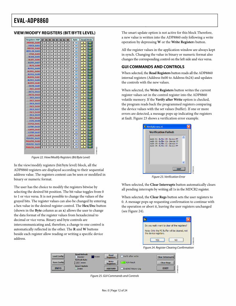
VIEW/MODIFY REGISTERS (BIT/BYTE LEVEL)
0798
8-02
2
All the register values in the application window are always kept in synch. Changing the value in binary or numeric format also changes the corresponding control on the left side and vice versa.
GUI COMMANDS AND CONTROLS When selected, the Read Registers button reads all the ADP8860 internal registers (Address 0x00 to Address 0x24) and updates the controls with the new values.
When selected, the Write Registers button writes the current register values set in the control register into the ADP8860 volatile memory. If the Verify after Write option is checked, the program reads back the programmed registers comparing the device values with the set values (buffer). If one or more errors are detected, a message pops up indicating the registers at fault. Figure 23 shows a verification error example.
0798
8-02
4
Figure 22. View/Modify Registers (Bit/Byte Level)
In the view/modify registers (bit/byte level) block, all the ADP8860 registers are displayed according to their sequential address value. The registers content can be seen or modified in binary or numeric format.
Figure 23. Verification Error
When selected, the Clear Interrupts button automatically clears all pending interrupts by writing all 1s in the MDCR2 register. The user has the choice to modify the registers bitwise by
selecting the desired bit position. The bit value toggles from 0 to 1 or vice versa. It is not possible to change the values of the grayed bits. The register values can also be changed by entering a hex value in the desired register control. The Hex/Dec button (shown in the Byte column as an x) allows the user to change the data format of the register values from hexadecimal to decimal or vice versa. Binary and byte controls are intercommunicating and, therefore, a change to one control is automatically reflected in the other. The R and W buttons beside each register allow reading or writing a specific device address.
When selected, the Clear Regs button sets the user registers to 0. A message pops up requesting confirmation to continue with the operation or abort it, leaving the user registers unchanged (see Figure 24).
0798
8-02
5
Figure 24. Register Clearing Confirmation
0798
8-02
3
Figure 25. GUI Commands and Controls

EVAL-ADP8860
Rev. 0 | Page 13 of 24
The Read Refresh option enables the program to read the device status periodically. The refresh time is programmable in the Refresh Rate window from 100 ms to 5 sec. The registers read during the refresh are MFDVID (Address 0x00), MDCR (Address 0x01), CCFG (Address 0x1B), CCFG2 (Address 0x1C), PH1LEVL (Address 0x21), PH1LEVH (Address 0x22), PH2LEVL (Address 0x23), and PH2LEVH (Address 0x24), providing a real-time indication of the device functionality. When the blue Access indicator lights up, it indicates that the refresh operation is taking place.
The Smart Update option enables the program to automatically write an ADP8860 register when a value has been changed, which avoids selecting the Write Registers button every time a value is changed. The Smart Update option must be unchecked if the user wants to control the writing operations.
LOAD/SAVE REGISTERS CONFIGURATION The software program allows saving a specific registers confi-guration and loading it back in the Register Controls and Registers MAP window (see Figure 14). The Save Config button opens the file utility. Here, it is possible to specify a directory and filename to save. The default extension is *.dat and it is suggested to maintain this convention. If the file does not exist, it is created. If the file already exists, it is overwritten.
0798
8-02
6
Figure 26. Save Configuration
The Load Config button opens the file utility where it is possible to specify a directory and filename to load. The default exten-sion is *.dat. Opting to cancel the operation prompts an error message. Press Continue to abort the operation (see Figure 27).
0798
8-02
7
Figure 27. Load/Save Error Message
ADDITIONAL COMMANDS The INFO button provides information regarding the software revision number and other release notes (see Figure 25).
The EXIT button stops the program but leaves the window active (see Figure 25). To terminate the program completely, select the X button on the top right of the application window.
Online help is available by clicking CTRL + H. Hovering the mouse over a control or indicator displays information related to it in the context help window.
HISTORY Whenever issuing a command (both read and write), it is recorded in the History dialog box shown in Figure 28.
To display the History dialog box, click the HISTORY menu in the main software dialog box (see Figure 15) or the Windows® History tab on the bottom. To clear the history, click Clear History.
The window content can be copied and pasted into a text editor and then saved for future evaluation purposes.
0798
8-02
8
Figure 28. History

EVAL-ADP8860
Rev. 0 | Page 14 of 24
EVALUATION BOARD OVERVIEW MOTHERBOARD
INT/EXT SUPPLIESJUMPER SELECTION
VBATT LEDINDICATOR
VDDIO LEDINDICATOR
VBOARD LEDINDICATOR
RESET (nRST)PUSHBUTTON
EXTERNALTARGET
CONNECTOR
BACKLIGHT LEDS (7 MAXIMUM) ANDINDIVIDUAL JUMPERS SELECTION
BACKLIGHT/KEYPADLED SELECTION JUMPER
KEYPAD LEDS (10 MAXIMUM) ANDINDIVIDUAL JUMPERS SELECTION(UP TO THREE CURRENT LEVELS)
PHOTOTRANSISTORSBIAS VOLTAGE JUMPERSELECTION
0798
8-02
9
EXTERNAL SUPPLIES USB CONNECTOR
DAUGHTER BOARDCONNECTORS
Figure 29. Motherboard
The EVAL-ADP8860 motherboard provides the interface signals to the ADP8860 parallel backlight IC. These include the SDA and SCL lines for I2C or the control line voltages for the hardware interface modes (nRST and nINT).
The CY68013A from Cypress Semiconductor Corporation provides the USB interface and I2C signals. The selected I2C frequency is 100 kHz. The M24C64R serial EEPROM provides the USB address of the board. The interface voltage is selected with the VBOARD header on the board and is set to 3.3 V by default.
Typically, the daughterboard is inserted directly into the 2 × 20 pin header of the motherboard. The 8-pin header, J29, on the top of the motherboard can be used to connect external supplies.
The VBATT OKAY, VDDIO OKAY, and VBOARD OKAY LEDs located at the top left of the board light up when the board is powered from the USB cable or external supplies are connected to J29 and the LK1 to LK3 jumpers are set in the EXT position. It is possible to choose several supply combi-nations. For example VBOARD, which supplies the motherboard ICs, can be provided from the USB while VDDIO and VBATT are provided externally. The motherboard contains three LDOs, generating the default supply voltage as indicated in Table 1.
Table 1. Power Supply Options
Supply Line LK8 to LK10 in USB Position
LK8 to LK10 in EXT Position
VBATT Internal: 3.7 V External: 2.3 V to 5.5 V VDDIO Internal: 2.7 V External: 1.7 V to 5.5 V VBOARD Internal: 3.3 V External: 2.7 V to 3.6 V
Jumper LK4 selects the supply voltage for the daughterboard phototransistors. With the jumper in EXT_VS position, the supply voltage +VS comes from the external target. With the jumper in VBOARD position, +VS is supplied by the VBOARD rail.

EVAL-ADP8860
Rev. 0 | Page 15 of 24
The VDDIO supply line determines the logic levels for nRST, nINT, SDA, and SCL.
When shunted, Jumper J31 and Jumper J32 connect the Cypress I2C interface to the daughterboard, which is the default setting for PC-to-adapter board communication. J31 and J32 must be removed if the I2C interface (master) is provided from the target (J30) to avoid bus contention.
JP1 selects the Sink 7 usage mode. If JP1 is in the LED position, Sink 7 is connected to the D15 LED and can be used as individ-ual sink or as part of the backlight. If JP1 is in the KEYPD BL position, Sink 7 is connected to the keyboard light LED block.
For demonstration purposes the adapter board contains two LED lighting sections: the display backlight and the keypad backlight. The former can be configured, through jumper selection, to drive up to seven LEDs with up to 30 mA per LED. The second LED section contains up to 10 LEDs with a jumper-programmable current range. For example, D2 has two jumpers associated with it: J6 and J7. D2 is disabled by removing both jumpers. If only J6 is installed, D2 has a 100 Ω limiting (ballast) resistor. If only J7 is installed, D2 has a 50 Ω limiting resistor. If both jumpers are installed, the limiting resistor is the parallel of two resistors or 33.3 Ω. The lower is the limiting resistor; the higher is the driving capability per LED. The same applies for all the other LEDs used for the keypad backlight.
It is possible to measure the total LEDs current by removing the J1 and J2 jumpers and inserting a current meter across one of the jumpers. Each LED current can be measured by removing the individual LED selection (that is, J5 for D5, Sink 1 LED) and inserting an ammeter. The ADP8860 input current can be measured by removing Jumper LK6 in the daughterboard and inserting a current meter across the jumper.
An external target hardware can be connected to the adapter and daughterboard using a J30 connector. The signals available are indicated in Figure 30.
GROUND (GND)
PHOTOTRANSISTOR SUPPLY VOLTAGE (+VS)
GROUND (GND)
EXTERNAL PHOTOTRANSISTOR 2 (I_PHS2)
GROUND (GND)
EXTERNAL PHOTOTRANSISTOR 1 (I_PHS1)
GROUND (GND)
LOGIC VOLTAGE LEVEL (VDDIO)
RESET INPUT (nRST)
INTERRUPT OUTPUT (nINT)
I2C SERIAL CLOCK LINE (SCL)
I2C SERIAL DATA LINE (SDA)
BATTERY VOLTAGE SUPPLY (VBATT)
CHARGE-PUMP OUTPUT VOLTAGE (VOUT)
SINK 7 – LED7 ANODE
SINK 7 – LED7 CATHODE
SINK 6 – LED6 ANODE
SINK 6 – LED6 CATHODE
SINK 5 – LED5 ANODE
SINK 5 – LED5 CATHODE
SINK 4 – LED4 ANODE
SINK 4 – LED4 CATHODE
SINK 3 – LED3 ANODE
SINK 3 – LED3 CATHODE
SINK 2 – LED2 ANODE
SINK 2 – LED2 CATHODE
SINK 1 – LED1 ANODE
SINK 1 – LED1 CATHODE
28
26
24
22
20
18
16
14
12
10
8
6
4
2
27
25
23
21
19
17
15
13
11
9
7
5
3
1
J30
0798
8-03
0
Figure 30. Target Connector J30
The target can either control the circuit in the adapter board or be driven by the daughterboard, such as when the LEDs reside on the target board. Also, I2C commands can be sent in either direction. When the target provides the I2C interface, however, the J31 and J32 jumpers must be removed.

EVAL-ADP8860
Rev. 0 | Page 16 of 24
DAUGHTERBOARD
0798
8-03
3
Figure 31. Daughterboard
The ADP8860 evaluation daughterboard is designed to quickly evaluate key parameters of the ADP8860 IC. The board layout footprint is extended so that parts can be exchanged easily, and headers are available to measure currents using a current probe or ammeter.
Connect a power supply or Li-Ion battery with 1 A maximum current capability to VBATT (see Figure 29). Short thick cables are recommended to minimize the IR drops. A high current can cause a big IR drop, and VBATT can be low enough to put the part into UVLO.
LK2, LK3, LK4, and LK5 enable 10 kΩ pull-ups on nRST, nINT, SDA, and SCL, respectively. The pull-ups are referred to as the VDDIO supply.
Jumper JP6 must be installed in the PHS2 position if both phototransistors are used. In addition, Jumper J16 in the motherboard must be removed to disconnect LED6 from the second comparator input. In this configuration, the ADP8860 supports only six LEDs. Make sure to set the D6 Config checkbox in the GUI to enable the second comparator (see Figure 15 and Figure 16).
Quiescent Current Measurement
The ADP8860 has only one supply line (VIN) coming from the external supply. The input current can be measured by removing Jumper LK6 and inserting a current meter across the jumper.
EVAL-ADP8860
Rev. 0 | Page 17 of 24
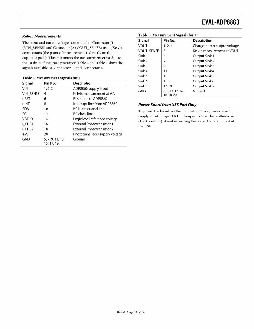
Kelvin Measurements
The input and output voltages are routed to Connector J1 (VIN_SENSE) and Connector J2 (VOUT_SENSE) using Kelvin connections (the point of measurement is directly on the capacitor pads). This minimizes the measurement error due to the IR drop of the trace resistance. Table 2 and Table 3 show the signals available on Connector J1 and Connector J2.
Table 2. Measurement Signals for J1 Signal Pin No. Description VIN 1, 2, 3 ADP8860 supply input VIN_SENSE 4 Kelvin measurement at VIN nRST 6 Reset line to ADP8860 nINT 8 Interrupt line from ADP8860 SDA 10 I2C bidirectional line SCL 12 I2C clock line VDDIO 14 Logic level reference voltage I_PHS1 16 External Phototransistor 1 I_PHS2 18 External Phototransistor 2 +VS 20 Phototransistors supply voltage GND 5, 7, 9, 11, 13,
15, 17, 19 Ground
Table 3. Measurement Signals for J2 Signal Pin No. Description VOUT 1, 2, 4 Charge-pump output voltage VOUT_SENSE 3 Kelvin measurement at VOUT Sink 1 5 Output Sink 1 Sink 2 7 Output Sink 2 Sink 3 9 Output Sink 3 Sink 4 11 Output Sink 4 Sink 5 13 Output Sink 5 Sink 6 15 Output Sink 6 Sink 7 17, 19 Output Sink 7 GND 6, 8, 10, 12, 14,
16, 18, 20 Ground
Power Board from USB Port Only
To power the board via the USB without using an external supply, short Jumper LK1 to Jumper LK3 on the motherboard (USB position). Avoid exceeding the 500 mA current limit of the USB.

EVAL-ADP8860
Rev. 0 | Page 18 of 24
EVALUATION BOARD SCHEMATICS AND ARTWORK
USB_VBATT
USB_VDDIO
EX
T_V
DD
IO
EX
T_V
BA
TT
D+D-
EX
T_V
BO
AR
D
USB_VBOARD
SD
A
SC
L
I_P
HS
2
nRS
TnI
NT
I_P
HS
1
SD
AS
CL
VD
DIO
VO
UT
VO
UT_
Sen
seS
ink1
Sin
k2S
ink3
Sin
k4
Sin
k6S
ink7
Sin
k5
SD
AS
CL
nIN
TnR
ST
VD
DIO I_
PH
S1
VB
ATT I_
PH
S2
VIN
_SE
NS
E
VB
ATT
VD
DIO
VB
OA
RD
VB
OA
RD
VB
OA
RD
VB
OA
RDVB
OA
RD
VB
OA
RD
VB
OA
RD
VB
OA
RD
VB
OA
RD
VB
OA
RD
VB
OA
RD
VD
DIO
VD
DIO
VB
OA
RD
VB
OA
RD
Sin
k2
Sin
k3
Sin
k4
Sin
k5
Sin
k6
Sin
k7
VO
UT
Sin
k1
nIN
TnR
ST
VD
DIO
VB
ATT
3.6V
2.7V
3.3V 1208
SDA
SCL
VIN
VOUT
EXT_VS
+VS
GND
GND
GND
GND
Mous
er
p/n
Mou
ser
p/
n
C15
2.2
uF
U3
AD
P17
15/1
6
U3
EN
1
IN2
OU
T3
AD
J/S
S/T
RK
4G
ND
45
GN
D3
6G
ND
27
GN
D1
8
D21
LED
LK3
2 W
ay L
ink
13
2
C13
2.2u
F
C11
2.2u
F
C25
0.1u
F
TP6 1
Y1
CR
YS
TA
L14
Y1
13
42
C4
0.1u
F
R36
10k
C24
47 u
F
TP11 1
J33
1 3 5 7 9 11 13 15 17 19
2 4 6 8 10 12 14 16 18 20
C10
100n
F
C18
2.2
uF
C19
2.2
uF
C21
0.1u
F
U4
AD
P17
15/1
6
EN
1
IN2
OU
T3
AD
J/S
S/T
RK
4G
ND
45
GN
D3
6G
ND
27
GN
D1
8
TP7
1
R29
100k
R35
31.6
k
TP12
1
C14
2.2
uF
U2
AD
P17
15/1
6
EN
1
IN2
OU
T3
AD
J/S
S/T
RK
4G
ND
45
GN
D3
6G
ND
27
GN
D1
8
TP4
1
LK4
2 W
ay L
ink
1 3
2
R33
24.3
K
C8
0.1u
F
C22
2.2
uF
R27
100k
C20
2.2
uF
R25
680
TP8
1
TP9
TP9
1
D23
CG
0603
MLC
-05E
652-
CG
0603
MLC
-05E
652-
CG
0603
MLC
-05E
U5
M24
AA
64-R
A0
A1
A2
VSSSDA
SCL
WP
VCC
TP5
1
J34
J34
1 3 5 7 9 11 13 15 17 19
2 4 6 8 10 12 14 16 18 20
D19
LED
C6
6.2p
F
R37
2.2k
R30
36.5
k
R24
100k
TP10 1
J31
J31
12
JP2
US
B-m
iniB
VD
D(V
BU
S)
1
D-
2
D+
3
ID4
GN
D5
MS
16
MS
27
MS
38
MS
49
X7
10
X8
11
D24
CG
0603
MLC
-05E
652-
CG
0603
MLC
-05E
652-
CG
0603
MLC
-05E
R38
2.2k
C16
0.1u
F
C26
0.1u
F
C9
6.2p
F
D22
MB
R05
30
LK1
2 W
ay L
ink
13
2C
710
uF
J32
J32
12
R31
10k
R40 4.7
C17
0.1u
F
J29
CO
N4J29
CO
N4
1 2 3 4
C5
0.1u
F
LK2
2 W
ay L
ink
13
2
R32
10k
TP3
1
C12
100n
F
U1
CY
7C68
013A
U1
CY
7C68
013A
RD
Y0/
SLR
D1
RD
Y1/
SLW
R2
AV
CC
13
XTA
LOU
T4
XTA
LIN
5
AG
ND
16
AV
CC
27
D+
8
D-
9
AG
ND
210
VC
C1
11
GN
D1
12
IFC
LK13
RE
S14
SCL 15
SDA 16
VCC2 17
PB0/FD0 18
PB1/FD1 19
PB2/FD2 20
PB3/FD3 21
PB4/FD4 22
PB5/FD5 23
PB6/FD6 24
PB7/FD7 25
GND2 26
VCC3 27
GND3 28
CTL
029
CTL
130
CTL
231
VC
C4
32P
A0/
INT1
33P
A1/
INT1
34
PA
3/*W
U2
36P
A4/
FIFO
AD
R0
37P
A5/
FIFO
AD
R1
38P
A6/
*PK
TEN
D39
PA
7/*F
LAG
40G
ND
441
RE
SE
T42
PA
2/*S
LOE
35
VCC543*WAKEUP44
PD0/FD845PD1/FD946PD2/FD947
PD3/FD1048PD4/FD1149PD5/FD1250PD6/FD1351PD7/FD1452
GND553CLKOUT54
VCC655GND656
PD
PA
D
R39 4.7
R26
680
R28 680
C23
0.1u
F
J30 con2
8
2 4 6 8 10 12 14 16 18 20 22 24 26 28
1 3 5 7 9 11 13 15 17 19 21 23 25 27
R34
10k
D20
LED
07988-031
Figure 32. Motherboard Schematic—Main Section

EVAL-ADP8860
Rev. 0 | Page 19 of 24
nRST
VDD
IO
nIN
T
VBO
ARD
VDD
IO
Sink
1
Sink
2
Sink
3
Sink
4
Sink
5
Sink
6
Sink
7
VOU
T
12
3
45
6
78
9
*0
#
INT
nRST
nINT
Single LED
Keypad BL
Keypad Backlight
Display Backlight
ISNK1
ISNK2
ISNK3
ISNK4
ISNK5
ISNK6
ISNK7
IOUT
Make
sur
e to
use
the
cor
rect
foo
tpri
nt f
or Q
1
Q1
FDN
335N
SOT2
3
Q1
FDN
335N
SOT2
3
D10
BLU
ED
10BL
UE
R8
49
.9
R8
49
.9
R13
49
.9
R13
49
.9
R2
49
.9R
24
9.9
D8
D8
J28
J28
1 2
J13
J13
12
R6
49
.9
R6
49
.9
R12
100
R12
100
J8J8
1 2
R15
49
.9
R15
49
.9
D9
BLU
ED
9BL
UE
C1 0.1u
FD
NI
C1 0.1u
FD
NI
J16
J16
12
J9J9
1 2
J18
J18
1 2
D7
D7
R3
220
R3
220
J20
J20
1 2
TP2
TP2
1
J17
J17
1 2
J27
J27
1 2
R1
10
0R
11
00
D5
LED
D5
LED
R7
100
R7
100
D6
D6
J3J31
2
JP1
INTF
INTF1
12
23
3
D3
BLU
ED
3BL
UE
J15
J15
12
R17
49
.9
R17
49
.9D
14D
14
D15
D15
J19
J19
1 2
R22
100
R22
100
J23
J23
1 2
R4
10k
R4
10k
D2
BLU
ED
2BL
UED
1BL
UE
D1
BLU
E
D18
BLU
ED
18BL
UE
J22
J22
1 2
J1J11
2
R20
100
R20
100
D13
D13
R19
49
.9
R19
49
.9
R10
49
.9
R10
49
.9
J4J41
2
TP1
TP1
1
J12
J12
12
J14
J14
12
D17
BLU
ED
17BL
UE
R21
49
.9
R21
49
.9
J6J6
1 2
R18
100
R18
100
R16
100
R16
100
S1S13
4
21
J10
J10
1 2
R11
10k
R11
10k
R9
100
R9
100
J5J51
2
R5
100
R5
100
J21
J21
1 2
J7J7
1 2
D12
D12
J24
J24
1 2
D11
BLU
ED
11BL
UE
R23
49
.9
R23
49
.9
D4
BLU
ED
4BL
UE
J11
J11
1 2
D16
BLU
ED
16BL
UE
R14
100
R14
100
J26
J26
1 2
J2J21
2
J25
J25
1 2
07988-032
Figure 33. Motherboard Schematic—Interface Section

EVAL-ADP8860
Rev. 0 | Page 20 of 24
nRST
nIN
TSD
ASC
L
Sink
1Si
nk2
Sink
3Si
nk4
VDD
IO
VIN
VOU
T
+VS
Sink
5
VIN
_SEN
SE
Sink
6
VOU
T_Se
nse
nINT nR
STSD
A
SCL
VIN
C1+
C1-C2+
C2-
VOUT
CMP1CMP2
IVIN
PHS2
VPHS
_SEL
VOUT
+VS
PUP-
nRST
PUP-
nINT
PUP-
SCL
PUP-
SDA
GND
AGND
GND
GND
VDDIO
VPHS
Make
sur
e th
at D
1/GN
D2 i
s th
e AG
ND
Sink
6
D6_S
ELU
1AD
P886
0U
1AD
P886
0
D1
D3
D2
E3
D3
E4
D4
D4
D5
C4
D6/
CM
P_I
N2
B4
D7
B3
C1+A1
C1-C1
C2+B1
C2-B2
VOUTA2
VIN
A3
RS
TE
1
INT
D2
SD
AC
2
SC
LE
2
GND1A4
GND2D1
CM
P_I
NC
3
C1
1UF/
16V
J11 3 5 7 9 11 13 15 17 19
2 4 6 8 10 12 14 16 18 20
TP91
TP15
1
TP1
1
C5
1UF/
16V
TP13
1
TP14
1
TP7
TP7 1
TP20
1
C4
0.1U
FC
70.
1UF
DN
I
TP8
1
TP16
1
TP4 1
TP2 1
TP6
1
TP101
C6
0.1U
F
R2
10
K
R3
10
K
TP17
1J2
1 3 5 7 9 11 13 15 17 19
2 4 6 8 10 12 14 16 18 20
R4
10
KLK
5 12
TP21
1
TP121
D2
APD
S-90
05
LK4 1
2
LK3 1
2
R1
10
KLK
2 12
D3
APD
S-90
05
TP5
1
TP111
TP3 1
LK6
12
TP19
1
JP6
INTF
11
22
3
3
C3
10U
F
TP18 1
JP5
INTF
11
22
3
3
C2
1UF/
16V
07988-034
Figure 34. Daughterboard Schematic

EVAL-ADP8860
Rev. 0 | Page 21 of 24
PCB LAYOUT
0798
8-03
9
Figure 35. Motherboard, Top Layer
0798
8-04
0
Figure 36. Motherboard, Inner Layer 1
0798
8-04
1
Figure 37. Motherboard, Inner Layer 2
0798
8-04
2
Figure 38. Motherboard, Bottom Layer

EVAL-ADP8860
Rev. 0 | Page 22 of 24
0798
8-03
5Figure 39. Daughterboard, Top Layer
0798
8-03
6
Figure 40. Daughterboard, Inner Layer 1
0798
8-03
7
Figure 41. Daughterboard, Inner Layer 2
0798
8-03
8
Figure 42. Daughterboard, Bottom Layer

EVAL-ADP8860
Rev. 0 | Page 23 of 24
ORDERING INFORMATION BILL OF MATERIALS
Table 5. Motherboard Qty Reference Designator Description Manufacturer/Vendor Part Number 12 C1, C4, C5, C8, C10, C12, C16,
C17, C21, C23, C25, C26 100 nF, 10 V, 0402, X5R, MLCC capacitor Murata Manufacturing Co., Ltd. GRM155R61A104KA01B
2 C6, C9 6.0 pF, 0402, NP0, MLCC capacitor Vishay/Panasonic ECJ0EC1H060D 1 C7 10 μF, 6.3 V, 0603, X5R, MLCC capacitor Murata Manufacturing Co., Ltd. GRM188R60J106ME 8 C11, C13, C14, C15, C18, C19,
C20, C22 2.2 μF, 10 V, 0603, X5R, MLCC capacitor Murata Manufacturing Co., Ltd. GRM188R61A225K
1 C24 47 μF, 16 V, 1210 X5R, MLCC capacitor Murata Manufacturing Co., Ltd. GRM32ER61C476K 10 D1, D2, D3, D4, D9, D10, D11,
D16, D17, D18 Blue 0805, SMD, LED Lumex Inc. SML-LX0805USBC-TR
1 D5 Red, 0805, SMD LED Lumex Inc. SML-LXT0805IW-TR 7 D6, D7, D8, D12, D13,
D14, D15 White, 0805, SMD LED Osram LW M67C-S1T2-5K8L-Z
3 D19, D20, D21 Green, 0805, SMD LED Lumex Inc. SML-LXT0805GW-TR 1 D22 Schottky diode, SC70 ON Semiconductor MBR0530T1G 2 D23, D24 USB ESD protector Bourns CG0603MLC-05E 10 R1, R5, R7, R9, R12, R14, R16,
R18, R20, R22 100 Ω, 1%, 0603, SMD, resistor Vishay Dale or equivalent CRCW0603100RFKE
10 R2, R6, R8, R10, R13, R15, R17, R19, R21, R23
49.9 Ω, 1%, 0402, SMD resistor Panasonic or equivalent ERJ-2RKF49R9X
1 R3 220 Ω, 1%, 0603, SMD resistor Vishay Dale or equivalent CRCW0603220RFKE 6 R4, R11, R31, R32, R34, R36 10 kΩ, 1%, 0603, SMD resistor Vishay Dale or equivalent CRCW040210022F 3 R24, R27, R29 100 kΩ, 1%, 0402, SMD resistor Vishay Dale or equivalent CRCW04021003F 3 R25, R26, R28 680 Ω, 1%, 0603, SMD resistor Vishay Dale or equivalent CRCW04026810F 1 R35 31.6 kΩ, 1%, 0402, SMD resistor Vishay Dale or equivalent CRCW04023162F 2 R39, R40 4.75 Ω, 1%, 0603, SMD resistor Vishay Dale or equivalent CRCW06034R75FKTA 1 R30 36.5 kΩ, 1%, 0603, SMD resistor Vishay Dale or equivalent CRCW060336K5FKE 1 R33 24.3 Ω, 1%, 0402, SMD resistor Vishay Dale or equivalent CRCW040224K3FKE 2 R37, R38 2.21 kΩ, 1%, 0402, SMD resistor Vishay Dale or equivalent CRCW04022211FRT1 1 U1 IC MCU USB peripheral high SPD-56QFN Cypress Semiconductor Corp CY7C68013A 3 U2, U3, U4 IC LDO regulator, 500 mA, 8-Lead MSOP Analog Devices, Inc. ADP1715/ADP1716 1 U5 Microchip Serial EEPROM-64K, MSOP8 Microchip M24LC64 or 24AA64 1 Y1 Crystal 24 MHz CTS Corporation CTX651CT 1 Q1 MOSFET N-channel, SOT23 Fairchild FDN335N 1 JP2 USB Connector USB Mini-B, 5-pin Delphi Corporation/Molex 15430262-110 30 J1 to J28, J31, J32 0.100, single, STR, 2-pin header Sullins Connector Solutions S1012-36-ND 1 J29 0.100, single, STR, 4-pin header Sullins Electronics, Inc. PEC36SAAN1 J30 0.100, dual, STR, 28-pin header Sullins Electronics, Inc. PEC14DAAN 2 J33, J34 Male 0.100, dual, STR, 2 × 10 pin header Sullins Connector Solutions PTC10SAAN 5 LK1, LK2, LK3, LK4, JP1 0.100, single, STR, 3-pin header Sullins Connector Solutions PEC03SAAN 1 S1 Push-button switch, SMD C & K Components KSC321JLFS

EVAL-ADP8860
Rev. 0 | Page 24 of 24
Table 4. Daughterboard Qty Reference Designator Description Manufacturer/Vendor Part Number 3 C1, C2, C5 1 μF, 10 V, 0603, X5R, MLCC capacitor Taiyo Yuden LMK107BJ105KK-T 1 C3 10 μF, 6.3 V, 0603, X5R, MLCC capacitor Taiyo Yuden JMK107BJ106MA 3 C4, C6, C7 100 nF, 10 V, 0402, X5R, MLCC capacitor Murata Manufacturing Co., Ltd. GRM155R61A104KA01B 4 R1, R2, R3, R4 10 kΩ, 1%, 0402 resistor Vishay Dale CRCW04021002F 2 D2, D3 6-pin chiplead phototransistor Avago APDS-9005-020 1 U1 20-ball, WLCSP ADP8860 Analog Devices ADP8860ACBZ-R7 2 J1, J2 0.100, double-row 10-pin header SAMTEC SSW-110-03-G-D 5 LK2, LK3, LK4, LK5, LK6 0.100, single, STR, 2-pin header Sullins Electronics, Inc./3M S1012-36-ND 2 JP5, JP6 0.100, single, STR, 3-pin header Sullins Electronics, Inc./3M S1012-36-ND
ORDERING GUIDE ESD CAUTION Model Description ADP886XADAPT-EVALZ1 Motherboard ADP8860DBCP-EVALZ1 Daughterboard—LFCSP Version ADP8860DBCB-EVALZ1 Daughterboard—WLCSP Version
1 Z = RoHS Compliant Part.
©2009 Analog Devices, Inc. All rights reserved. Trademarks and registered trademarks are the property of their respective owners. EB07988-0-7/09(0)