Adiabatic Technique for Energy Efficient Logic Circuits...
5
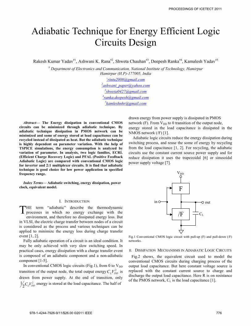
Abstract— The Energy dissipation in conventional CMOS circuits can be minimized through adiabatic technique. By adiabatic technique dissipation in PMOS network can be minimized and some of energy stored at load capacitance can be recycled instead of dissipated as heat. But the adiabatic technique is highly dependent on parameter variation. With the help of TSPICE simulations, the energy consumption is analyzed by variation of parameter. In analysis, two logic families, ECRL (Efficient Charge Recovery Logic) and PFAL (Positive Feedback Adiabatic Logic) are compared with conventional CMOS logic for inverter and 2:1 multiplexer circuits. It is find that adiabatic technique is good choice for low power application in specified frequency range. Index Terms— Adiabatic switching, energy dissipation, power clock, equivalent model. I. INTRODUCTION HE term “adiabatic” describe the thermodynamic processes in which no energy exchange with the environment, and therefore no dissipated energy loss. But in VLSI, the electric charge transfer between nodes of a circuit is considered as the process and various techniques can be applied to minimize the energy loss during charge transfer event [1, 2]. Fully adiabatic operation of a circuit is an ideal condition. It may be only achieved with very slow switching speed. In practical cases, energy dissipation with a charge transfer event is composed of an adiabatic component and a non-adiabatic component [1-5]. In conventional CMOS logic circuits (Fig.1), from 0 to V DD transition of the output node, the total output energy 2 DD L V C is drawn from power supply. At the end of transition, only 2 2 1 DD L V C energy is stored at the load capacitance. The half of drawn energy from power supply is dissipated in PMOS network (F). From V DD to 0 transition of the output node, energy stored in the load capacitance is dissipated in the NMOS network (/F) [1]. Adiabatic logic circuits reduce the energy dissipation during switching process, and reuse the some of energy by recycling from the load capacitance [1, 2]. For recycling, the adiabatic circuits use the constant current source power supply and for reduce dissipation it uses the trapezoidal [6] or sinusoidal power supply voltage [7]. Fig.1 Conventional CMOS logic circuit with pull-up (F) and pull-down (/F) networks. II. DISSIPATION MECHANISMS IN ADIABATIC LOGIC CIRCUITS Fig.2 shows, the equivalent circuit used to model the conventional CMOS circuits during charging process of the output load capacitance. But here constant voltage source is replaced with the constant current source to charge and discharge the output load capacitance. Here R is on resistance of the PMOS network, C L is the load capacitance [1]. Adiabatic Technique for Energy Efficient Logic Circuits Design Rakesh Kumar Yadav #1 , Ashwani K. Rana #2 , Shweta Chauhan #3 , Deepesh Ranka #4 , Kamalesh Yadav #5 # Department of Electronics and Communication, National Institute of Technology, Hamirpur Hamirpur (H.P)-177005, India 1 [email protected] 2 [email protected] 3 [email protected] 4 [email protected] 5 [email protected] T F /F V DD C L out in PROCEEDINGS OF ICETECT 2011 978-1-4244-7926-9/11/$26.00 ©2011 IEEE 776
Transcript of Adiabatic Technique for Energy Efficient Logic Circuits...
Abstract— The Energy dissipation in conventional CMOS
circuits can be minimized through adiabatic technique. By adiabatic technique dissipation in PMOS network can be minimized and some of energy stored at load capacitance can be recycled instead of dissipated as heat. But the adiabatic technique is highly dependent on parameter variation. With the help of TSPICE simulations, the energy consumption is analyzed by variation of parameter. In analysis, two logic families, ECRL (Efficient Charge Recovery Logic) and PFAL (Positive Feedback Adiabatic Logic) are compared with conventional CMOS logic for inverter and 2:1 multiplexer circuits. It is find that adiabatic technique is good choice for low power application in specified frequency range.
Index Terms— Adiabatic switching, energy dissipation, power clock, equivalent model.
I. INTRODUCTION HE term “adiabatic” describe the thermodynamic processes in which no energy exchange with the environment, and therefore no dissipated energy loss. But
in VLSI, the electric charge transfer between nodes of a circuit is considered as the process and various techniques can be applied to minimize the energy loss during charge transfer event [1, 2].
Fully adiabatic operation of a circuit is an ideal condition. It may be only achieved with very slow switching speed. In practical cases, energy dissipation with a charge transfer event is composed of an adiabatic component and a non-adiabatic component [1-5].
In conventional CMOS logic circuits (Fig.1), from 0 to VDD transition of the output node, the total output energy 2
DDLVC is drawn from power supply. At the end of transition, only
2
21
DDLVC energy is stored at the load capacitance. The half of
drawn energy from power supply is dissipated in PMOS network (F). From VDD to 0 transition of the output node, energy stored in the load capacitance is dissipated in the NMOS network (/F) [1].
Adiabatic logic circuits reduce the energy dissipation during switching process, and reuse the some of energy by recycling from the load capacitance [1, 2]. For recycling, the adiabatic circuits use the constant current source power supply and for reduce dissipation it uses the trapezoidal [6] or sinusoidal power supply voltage [7]. Fig.1 Conventional CMOS logic circuit with pull-up (F) and pull-down (/F) networks.
II. DISSIPATION MECHANISMS IN ADIABATIC LOGIC CIRCUITS
Fig.2 shows, the equivalent circuit used to model the conventional CMOS circuits during charging process of the output load capacitance. But here constant voltage source is replaced with the constant current source to charge and discharge the output load capacitance. Here R is on resistance of the PMOS network, CL is the load capacitance [1].
Adiabatic Technique for Energy Efficient Logic Circuits Design
Rakesh Kumar Yadav#1, Ashwani K. Rana#2, Shweta Chauhan#3, Deepesh Ranka#4, Kamalesh Yadav#5 # Department of Electronics and Communication, National Institute of Technology, Hamirpur
Hamirpur (H.P)-177005, India [email protected]
[email protected] [email protected]
[email protected] [email protected]
T
F
/F
VDD
CL
out in
PROCEEDINGS OF ICETECT 2011
978-1-4244-7926-9/11/$26.00 ©2011 IEEE 776
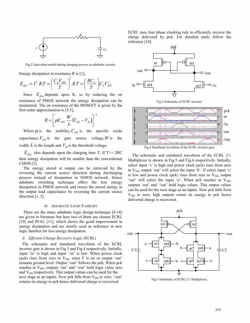
Fig.2 Equivalent model during charging process in adiabatic circuits.
Energy dissipation in resistance R is [1],
22
2 ..... DDLLDDL
diss VCT
RCTRTVCTRIE ⎟
⎠⎞
⎜⎝⎛=⎟
⎠⎞
⎜⎝⎛==
Since dissE depends upon R, so by reducing the on resistance of PMOS network the energy dissipation can be minimized. The on resistance of the MOSFET is given by the first order approximation is [3-5],
( )1−
⎥⎦⎤
⎢⎣⎡ −= thGSOX VV
LWCR μ
Where μ is the mobility, OXC is the specific oxide
capacitance, GSV is the gate source voltage,W is the
width, L is the length and thV is the threshold voltage.
dissE also depends upon the charging time T, If T>> 2RC then energy dissipation will be smaller than the conventional CMOS [1].
The energy stored at output can be retrieved by the reversing the current source direction during discharging process instead of dissipation in NMOS network. Hence adiabatic switching technique offers the less energy dissipation in PMOS network and reuses the stored energy in the output load capacitance by reversing the current source direction [1, 2].
III. ADIABATIC LOGIC FAMILIES
There are the many adiabatic logic design technique [8-18] are given in literature but here two of them are chosen ECRL [10] and PFAL [11], which shows the good improvement in energy dissipation and are mostly used as reference in new logic families for less energy dissipation.
A. Efficient Charge Recovery Logic (ECRL) The schematic and simulated waveform of the ECRL
inverter gate is shown in Fig.3 and Fig.4 respectively. Initially, input ‘in’ is high and input ‘/in’ is low. When power clock (pck) rises from zero to VDD, since F is on so output ‘out’ remains ground level. Output ‘/out’ follows the pck. When pck reaches at VDD, outputs ‘out’ and ‘/out’ hold logic value zero and VDD respectively. This output values can be used for the next stage as an inputs. Now pck falls from VDD to zero, ‘/out’ returns its energy to pck hence delivered charge is recovered.
ECRL uses four phase clocking rule to efficiently recover the charge delivered by pck. For detailed study follow the reference [10].
Fig.3 Schematic of ECRL inverter.
Fig.4 Simulated waveform of the ECRL inverter gate.
The schematic and simulated waveform of the ECRL 2:1
Multiplexer is shown in Fig.5 and Fig.6 respectively. Initially, select input ‘s’ is high and power clock (pck) rises from zero to VDD, output ‘out’ will select the input ‘b’. If select input ‘s’ is low and power clock (pck) rises from zero to VDD, output ‘out’ will select the input ‘a’. When pck reaches at VDD, outputs ‘out’ and ‘/out’ hold logic values. This output values can be used for the next stage as an inputs. Now pck falls from VDD to zero, high outputs return its energy to pck hence delivered charge is recovered.
Fig.5 Schematic of ECRL 2:1 Multiplexer.
m9
/b
out /out
s
/s
/a s
b
/s
aC1 C2
pck
m1 m2
m3 m4
m5 m6
m7 m8
m10
pck in
/in
out
/out
pck
/out out
m1 m
in /inm3 m4
CL
R
I
777
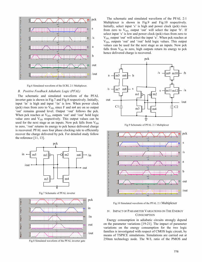
Fig.6 Simulated waveform of the ECRL 2:1 Multiplexer.
B. Positive Feedback Adiabatic Logic (PFAL) The schematic and simulated waveform of the PFAL
inverter gate is shown in Fig.7 and Fig.8 respectively. Initially, input ‘in’ is high and input ‘/in’ is low. When power clock (pck) rises from zero to VDD, since F and m4 are on so output ‘out’ remains ground level. Output ‘/out’ follows the pck. When pck reaches at VDD, outputs ‘out’ and ‘/out’ hold logic value zero and VDD respectively. This output values can be used for the next stage as an inputs. Now pck falls from VDD to zero, ‘/out’ returns its energy to pck hence delivered charge is recovered. PFAL uses four phase clocking rule to efficiently recover the charge delivered by pck. For detailed study follow the reference [11, 13].
Fig.7 Schematic of PFAL inverter
Fig.8 Simulated waveform of the PFAL inverter gate
The schematic and simulated waveform of the PFAL 2:1 Multiplexer is shown in Fig.9 and Fig.10 respectively. Initially, select input ‘s’ is high and power clock (pck) rises from zero to VDD, output ‘out’ will select the input ‘b’. If select input ‘s’ is low and power clock (pck) rises from zero to VDD, output ‘out’ will select the input ‘a’. When pck reaches at VDD, outputs ‘out’ and ‘/out’ hold logic values. This output values can be used for the next stage as an inputs. Now pck falls from VDD to zero, high outputs return its energy to pck hence delivered charge is recovered.
Fig.9 Schematic of PFAL 2:1 Multiplexer
Fig.10 Simulated waveform of the PFAL 2:1 Multiplexer
IV. IMPACT OF PARAMETER VARIATIONS ON THE ENERGY
CONSUMPTION
Energy consumption in adiabatic circuits strongly depend on the parameter variations [19-21]. The impact of parameter variations on the energy consumption for the two logic families is investigated with respect of CMOS logic circuit, by means of TSPICE simulations. Simulations are carried out at 250nm technology node. The W/L ratio of the PMOS and
/s
a b
s /a
/b /s
s
/out out
pck
C1 C2
m1 m2
m3 m4
m5 m6
m7 m8
m9 m10
m11 m12
m1 m2
m3 m4
m5 m6
pck
in
/out
/in
out
pck
s
/s
a
b
out
/out
pck
s
/s
a
b
out
/out
pck
in
/in
out
/out
778
NMOS are taken as λλ
29
and λ
λ2
3 respectively,
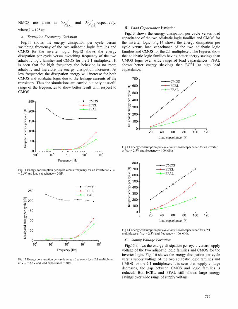
where nm125=λ . A. Transition Frequency Variation Fig.11 shows the energy dissipation per cycle versus
switching frequency of the two adiabatic logic families and CMOS for the inverter logic. Fig.12 shows the energy dissipation per cycle versus switching frequency of the two adiabatic logic families and CMOS for the 2:1 multiplexer. It is seen that for high frequency the behavior is no more adiabatic and therefore the energy dissipation increases. At low frequencies the dissipation energy will increase for both CMOS and adiabatic logic due to the leakage currents of the transistors. Thus the simulations are carried out only at useful range of the frequencies to show better result with respect to CMOS.
105 106 107 108 1090
50
100
150
200
250
Diss
ipat
ed e
nerg
y pe
r cyc
le [f
J]
Frequency [Hz]
CMOS ECRL PFAL
Fig.11 Energy consumption per cycle versus frequency for an inverter at VDD
= 2.5V and load capacitance = 20fF.
105 106 107 108 1090
50
100
150
200
250
Diss
ipat
ed e
nerg
y pe
r cyc
le [f
J]
Frequency [Hz]
CMOS ECRL PFAL
Fig.12 Energy consumption per cycle versus frequency for a 2:1 multiplexer at VDD = 2.5V and load capacitance = 20fF.
B. Load Capacitance Variation Fig.13 shows the energy dissipation per cycle versus load
capacitance of the two adiabatic logic families and CMOS for the inverter logic. Fig.14 shows the energy dissipation per cycle versus load capacitance of the two adiabatic logic families and CMOS for the 2:1 multiplexer. The Figures show that adiabatic logic families having better energy savings than CMOS logic over wide range of load capacitances. PFAL shows better energy shavings than ECRL at high load capacitance.
0 20 40 60 80 100 1200
100
200
300
400
500
600
700
Dis
sipat
ed e
nerg
y pe
r cyc
le [f
J]
Load capacitance [fF]
CMOS ECRL PFAL
Fig.13 Energy consumption per cycle versus load capacitance for an inverter at VDD = 2.5V and frequency = 100 MHz.
0 20 40 60 80 100 1200
100
200
300
400
500
600
700
800
Diss
ipat
ed e
nerg
y pe
r cyc
le [f
J]
Load capacitance [fF]
CMOS ECRL PFAL
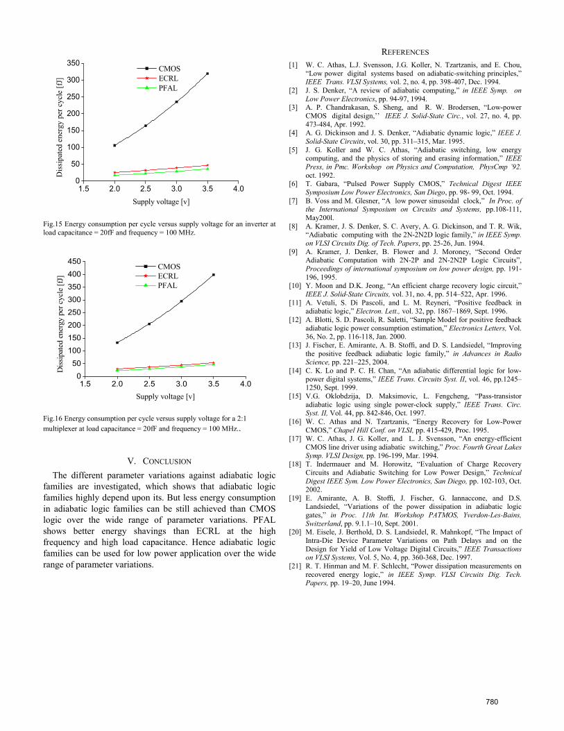
Fig.14 Energy consumption per cycle versus load capacitance for a 2:1 multiplexer at VDD = 2.5V and frequency = 100 MHz.
C. Supply Voltage Variation Fig.15 shows the energy dissipation per cycle versus supply
voltage of the two adiabatic logic families and CMOS for the inverter logic. Fig. 16 shows the energy dissipation per cycle versus supply voltage of the two adiabatic logic families and CMOS for the 2:1 multiplexer. It is seen that supply voltage decreases, the gap between CMOS and logic families is reduced. But ECRL and PFAL still shows large energy savings over wide range of supply voltage.
779
1.5 2.0 2.5 3.0 3.5 4.00
50
100
150
200
250
300
350D
issip
ated
ene
rgy
per c
ycle
[fJ]
Supply voltage [v]
CMOS ECRL PFAL
Fig.15 Energy consumption per cycle versus supply voltage for an inverter at load capacitance = 20fF and frequency = 100 MHz.
1.5 2.0 2.5 3.0 3.5 4.00
50
100150200250300350400450
Diss
ipat
ed e
nerg
y pe
r cyc
le [f
J]
Supply voltage [v]
CMOS ECRL PFAL
Fig.16 Energy consumption per cycle versus supply voltage for a 2:1 multiplexer at load capacitance = 20fF and frequency = 100 MHz..
V. CONCLUSION The different parameter variations against adiabatic logic
families are investigated, which shows that adiabatic logic families highly depend upon its. But less energy consumption in adiabatic logic families can be still achieved than CMOS logic over the wide range of parameter variations. PFAL shows better energy shavings than ECRL at the high frequency and high load capacitance. Hence adiabatic logic families can be used for low power application over the wide range of parameter variations.
REFERENCES [1] W. C. Athas, L.J. Svensson, J.G. Koller, N. Tzartzanis, and E. Chou,
“Low power digital systems based on adiabatic-switching principles,” IEEE Trans. VLSI Systems, vol. 2, no. 4, pp. 398-407, Dec. 1994.
[2] J. S. Denker, “A review of adiabatic computing,” in IEEE Symp. on Low Power Electronics, pp. 94-97, 1994.
[3] A. P. Chandrakasan, S. Sheng, and R. W. Brodersen, “Low-power CMOS digital design,’’ IEEE J. Solid-State Circ., vol. 27, no. 4, pp. 473-484, Apr. 1992.
[4] A. G. Dickinson and J. S. Denker, “Adiabatic dynamic logic,” IEEE J. Solid-State Circuits, vol. 30, pp. 311–315, Mar. 1995.
[5] J. G. Koller and W. C. Athas, “Adiabatic switching, low energy computing, and the physics of storing and erasing information,” IEEE Press, in Pmc. Workshop on Physics and Computation, PhysCmp ’92. oct. 1992.
[6] T. Gabara, “Pulsed Power Supply CMOS,” Technical Digest IEEE Symposium Low Power Electronics, San Diego, pp. 98- 99, Oct. 1994.
[7] B. Voss and M. Glesner, “A low power sinusoidal clock,” In Proc. of the International Symposium on Circuits and Systems, pp.108-111, May200l.
[8] A. Kramer, J. S. Denker, S. C. Avery, A. G. Dickinson, and T. R. Wik, “Adiabatic computing with the 2N-2N2D logic family,” in IEEE Symp. on VLSI Circuits Dig. of Tech. Papers, pp. 25-26, Jun. 1994.
[9] A. Kramer, J. Denker, B. Flower and J. Moroney, “Second Order Adiabatic Computation with 2N-2P and 2N-2N2P Logic Circuits”, Proceedings of international symposium on low power design, pp. 191-196, 1995.
[10] Y. Moon and D.K. Jeong, “An efficient charge recovery logic circuit,” IEEE J. Solid-State Circuits, vol. 31, no. 4, pp. 514–522, Apr. 1996.
[11] A. Vetuli, S. Di Pascoli, and L. M. Reyneri, “Positive feedback in adiabatic logic,” Electron. Lett., vol. 32, pp. 1867–1869, Sept. 1996.
[12] A. Blotti, S. D. Pascoli, R. Saletti, “Sample Model for positive feedback adiabatic logic power consumption estimation,” Electronics Letters, Vol. 36, No. 2, pp. 116-118, Jan. 2000.
[13] J. Fischer, E. Amirante, A. B. Stoffi, and D. S. Landsiedel, “Improving the positive feedback adiabatic logic family,” in Advances in Radio Science, pp. 221–225, 2004.
[14] C. K. Lo and P. C. H. Chan, “An adiabatic differential logic for low-power digital systems,” IEEE Trans. Circuits Syst. II, vol. 46, pp.1245–1250, Sept. 1999.
[15] V.G. Oklobdzija, D. Maksimovic, L. Fengcheng, “Pass-transistor adiabatic logic using single power-clock supply,” IEEE Trans. Circ. Syst. II, Vol. 44, pp. 842-846, Oct. 1997.
[16] W. C. Athas and N. Tzartzanis, “Energy Recovery for Low-Power CMOS,” Chapel Hill Conf. on VLSI, pp. 415-429, Proc. 1995.
[17] W. C. Athas, J. G. Koller, and L. J. Svensson, “An energy-efficient CMOS line driver using adiabatic switching,” Proc. Fourth Great Lakes Symp. VLSI Design, pp. 196-199, Mar. 1994.
[18] T. Indermauer and M. Horowitz, “Evaluation of Charge Recovery Circuits and Adiabatic Switching for Low Power Design,” Technical Digest IEEE Sym. Low Power Electronics, San Diego, pp. 102-103, Oct. 2002.
[19] E. Amirante, A. B. Stoffi, J. Fischer, G. Iannaccone, and D.S. Landsiedel, “Variations of the power dissipation in adiabatic logic gates,” in Proc. 11th Int. Workshop PATMOS, Yverdon-Les-Bains, Switzerland, pp. 9.1.1–10, Sept. 2001.
[20] M. Eisele, J. Berthold, D. S. Landsiedel, R. Mahnkopf, “The Impact of Intra-Die Device Parameter Variations on Path Delays and on the Design for Yield of Low Voltage Digital Circuits,” IEEE Transactions on VLSI Systems, Vol. 5, No. 4, pp. 360-368, Dec. 1997.
[21] R. T. Hinman and M. F. Schlecht, “Power dissipation measurements on recovered energy logic,” in IEEE Symp. VLSI Circuits Dig. Tech. Papers, pp. 19–20, June 1994.
780