Adiabatic Logic Circuit for Biomedical Applications Prepared by: Muhammad Arsalan Presented to: Dr....
47
Adiabatic Logic Circuit for Biomedical Applications Prepared by: Prepared by: Muhammad Arsalan Muhammad Arsalan Presented to: Presented to: Dr. Maitham Shams Dr. Maitham Shams
-
Upload
myles-price -
Category
Documents
-
view
225 -
download
0
Transcript of Adiabatic Logic Circuit for Biomedical Applications Prepared by: Muhammad Arsalan Presented to: Dr....
Adiabatic Logic Circuit for Biomedical Applications
Adiabatic Logic Circuit for Biomedical Applications
Prepared by:Prepared by:
Muhammad ArsalanMuhammad ArsalanPresented to:Presented to:
Dr. Maitham ShamsDr. Maitham Shams
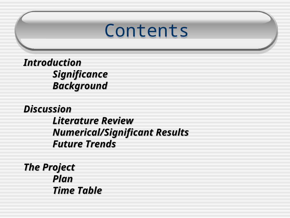
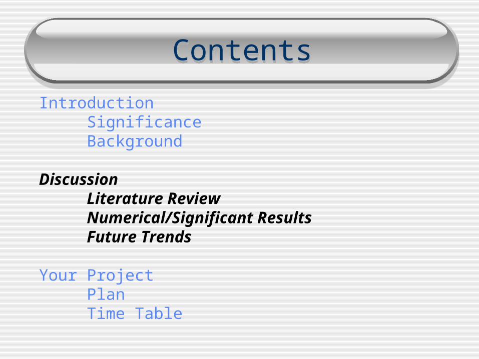
ContentsContents
IntroductionIntroductionSignificanceSignificanceBackgroundBackground
DiscussionDiscussionLiterature ReviewLiterature ReviewNumerical/Significant ResultsNumerical/Significant ResultsFuture TrendsFuture Trends
The ProjectThe ProjectPlanPlanTime TableTime Table
Low PowerLow Power
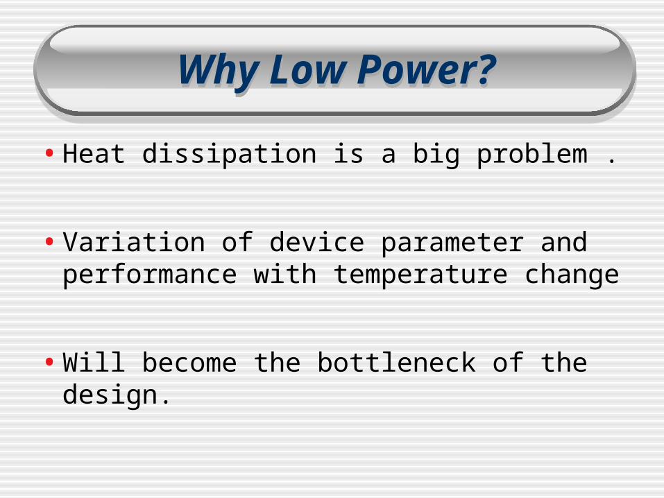
Why Low Power?Why Low Power?
• Heat dissipation is a big problem .
• Variation of device parameter and performance with temperature change
• Will become the bottleneck of the design.
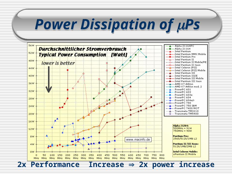
Power Dissipation of PsPower Dissipation of Ps
2x Performance Increase 2x power increase
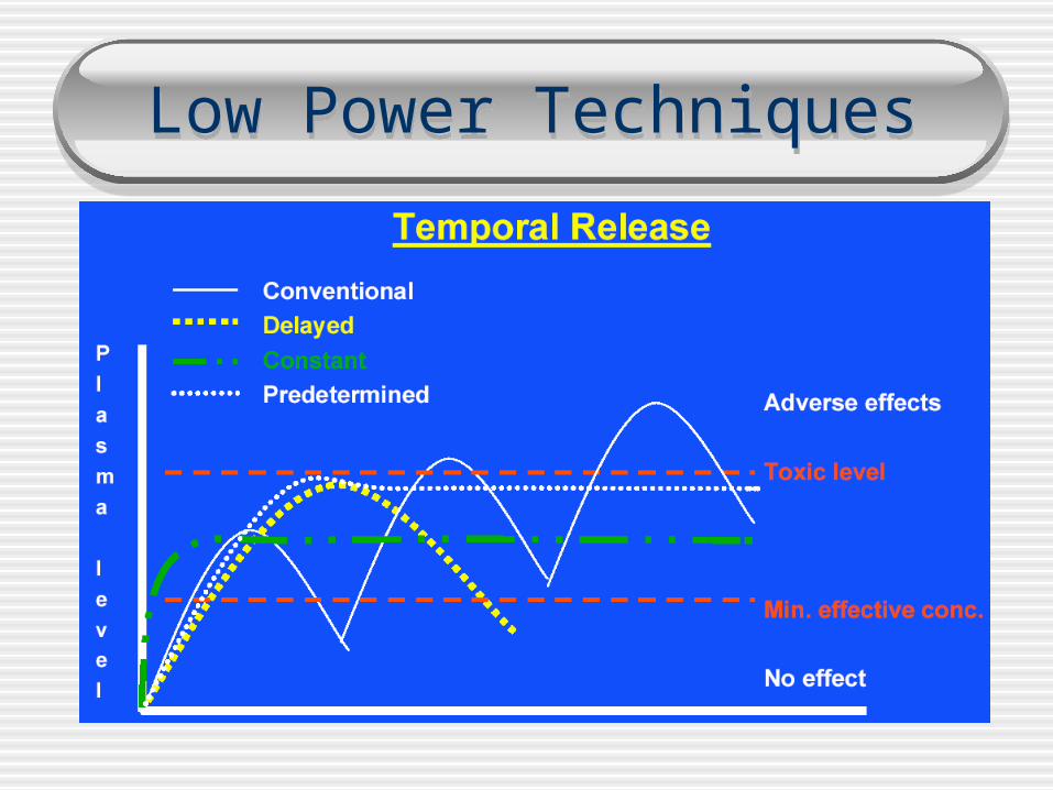
Low Power TechniquesLow Power Techniques
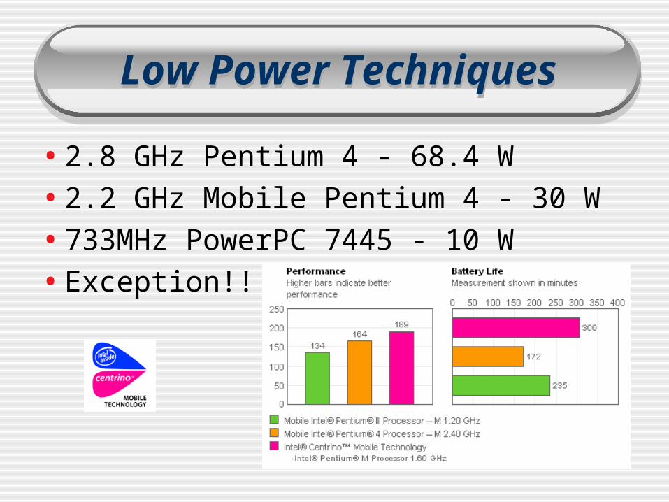
• 2.8 GHz Pentium 4 - 68.4 W
• 2.2 GHz Mobile Pentium 4 - 30 W
• 733MHz PowerPC 7445 - 10 W
• Exception!!
Low Power TechniquesLow Power Techniques
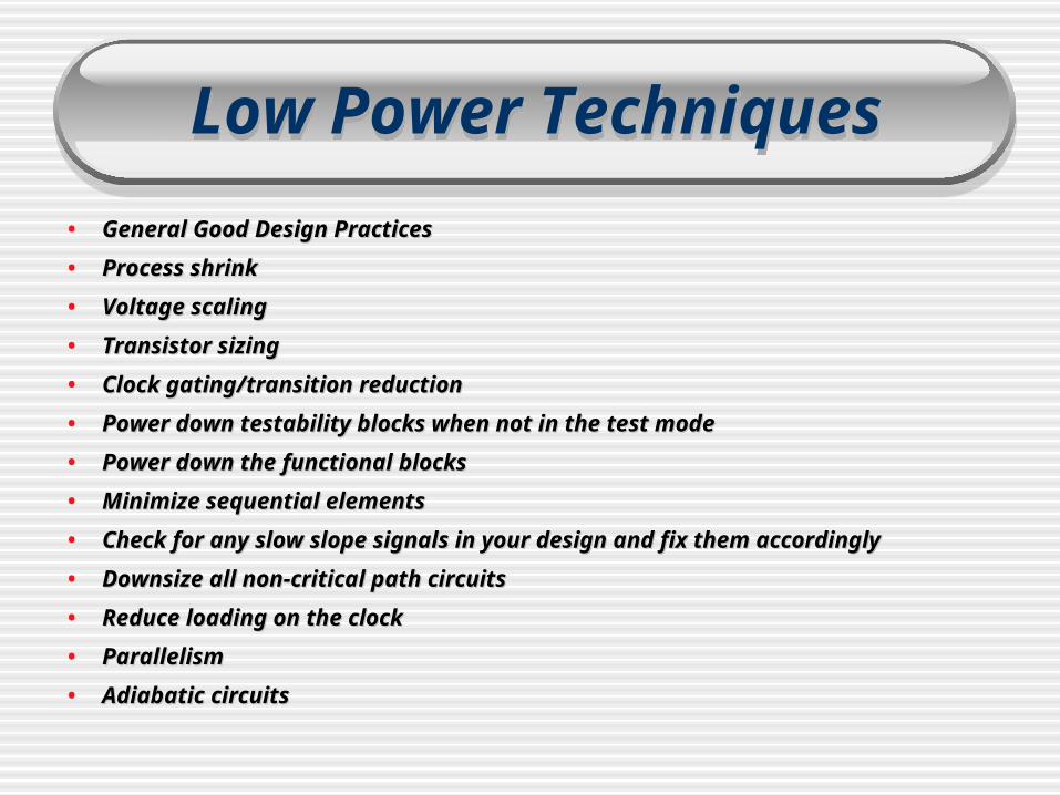
• General Good Design PracticesGeneral Good Design Practices
• Process shrinkProcess shrink
• Voltage scalingVoltage scaling
• Transistor sizingTransistor sizing
• Clock gating/transition reductionClock gating/transition reduction
• Power down testability blocks when not in the test modePower down testability blocks when not in the test mode
• Power down the functional blocksPower down the functional blocks
• Minimize sequential elementsMinimize sequential elements
• Check for any slow slope signals in your design and fix them accordinglyCheck for any slow slope signals in your design and fix them accordingly
• Downsize all non-critical path circuitsDownsize all non-critical path circuits
• Reduce loading on the clockReduce loading on the clock
• ParallelismParallelism
• Adiabatic circuitsAdiabatic circuits
Why Adiabatic Logic?Why Adiabatic Logic?
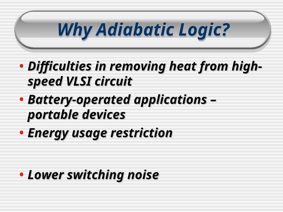
• Difficulties in removing heat from high-Difficulties in removing heat from high-speed VLSI circuitspeed VLSI circuit
• Battery-operated applications – Battery-operated applications – portable devicesportable devices
• Energy usage restrictionEnergy usage restriction
• Lower switching noiseLower switching noise
Power Dissipation in Conventional CMOS Inverter
Power Dissipation in Conventional CMOS Inverter
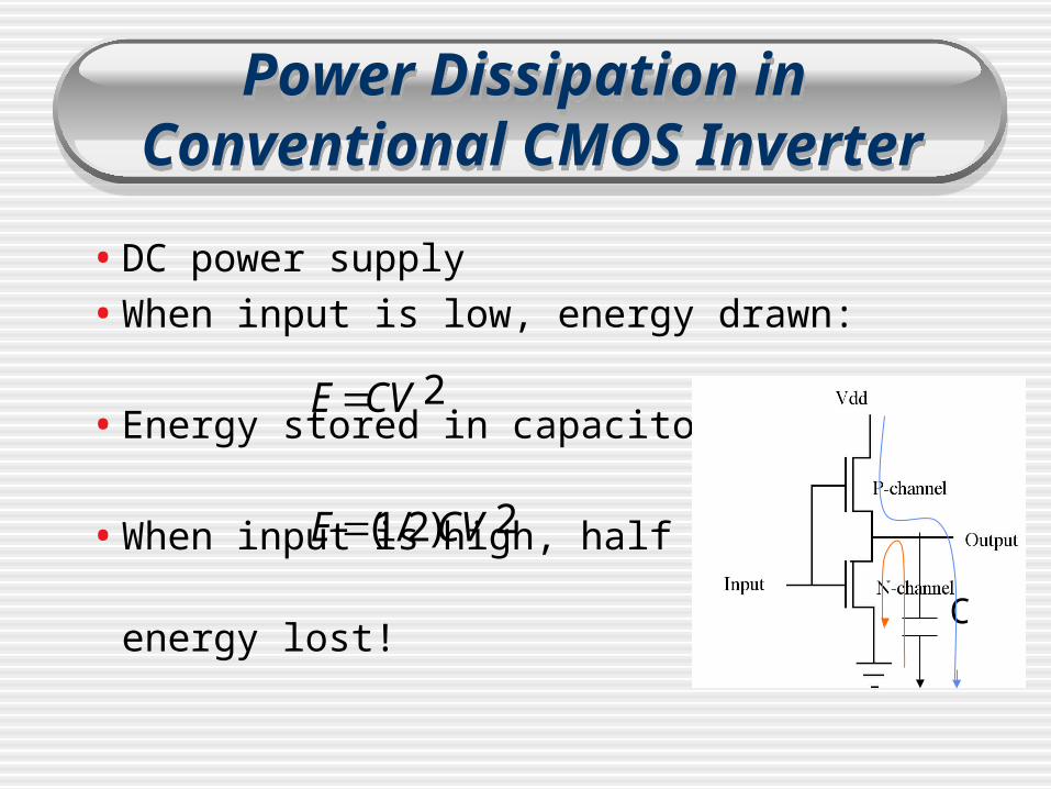
• DC power supply
• When input is low, energy drawn:
• Energy stored in capacitor:
• When input is high, half of
energy lost!
2CVE
2)2/1( CVE
C
Power Dissipation in AdiabaticPower Dissipation in Adiabatic
• Depends on configuration, will see in soon in this presentation
ContentsContents
IntroductionSignificanceBackground
DiscussionLiterature ReviewNumerical/Significant ResultsFuture Trends
Your ProjectPlanTime Table
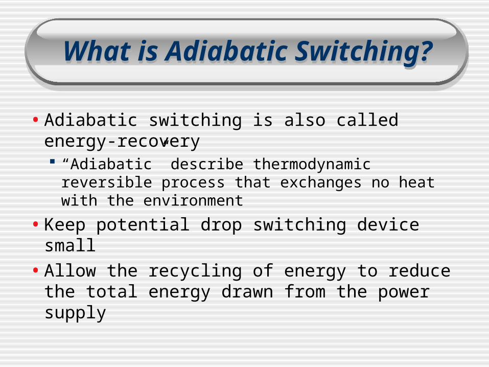
What is Adiabatic Switching?What is Adiabatic Switching?
• Adiabatic switching is also called energy-recovery “Adiabatic” describe thermodynamic reversible
process that exchanges no heat with the environment
• Keep potential drop switching device small
• Allow the recycling of energy to reduce the total energy drawn from the power supply
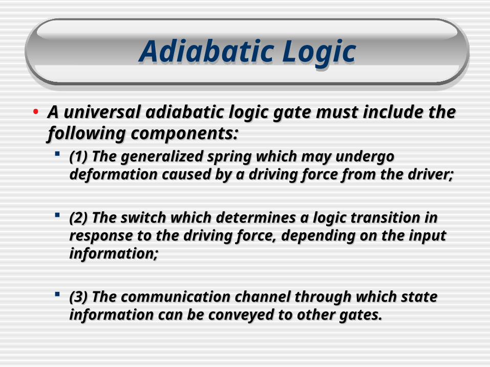
Adiabatic LogicAdiabatic Logic
• A universal adiabatic logic gate must include the A universal adiabatic logic gate must include the following components:following components: (1) The generalized spring which may undergo (1) The generalized spring which may undergo
deformation caused by a driving force from the driver;deformation caused by a driving force from the driver;
(2) The switch which determines a logic transition in (2) The switch which determines a logic transition in response to the driving force, depending on the input response to the driving force, depending on the input information;information;
(3) The communication channel through which state (3) The communication channel through which state information can be conveyed to other gates.information can be conveyed to other gates.
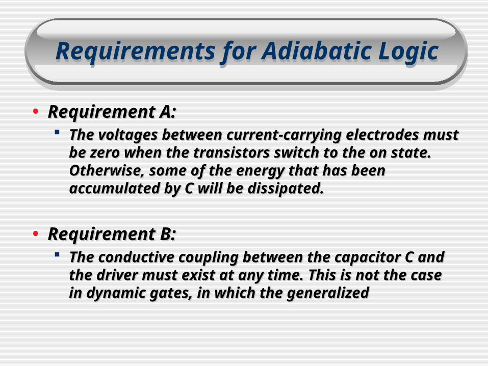
Requirements for Adiabatic LogicRequirements for Adiabatic Logic
• Requirement A:Requirement A: The voltages between current-carrying electrodes The voltages between current-carrying electrodes
must be zero when the transistors switch to the on must be zero when the transistors switch to the on state. Otherwise, some of the energy that has been state. Otherwise, some of the energy that has been accumulated by C will be dissipated.accumulated by C will be dissipated.
• Requirement B:Requirement B: The conductive coupling between the capacitor C and The conductive coupling between the capacitor C and
the driver must exist at any time. This is not the case the driver must exist at any time. This is not the case in dynamic gates, in which the generalizedin dynamic gates, in which the generalized
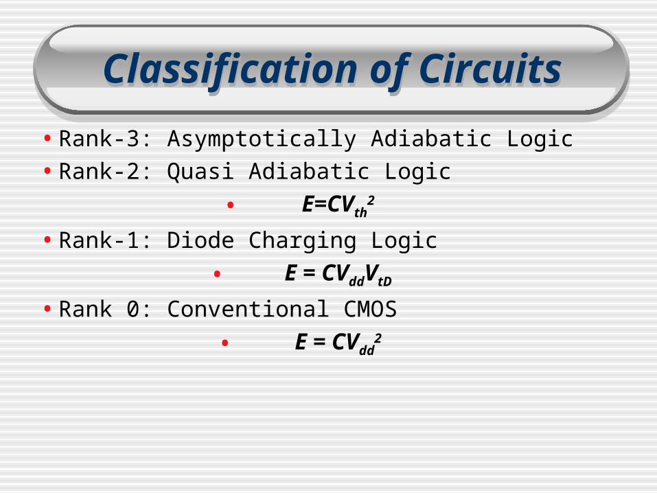
Classification of CircuitsClassification of Circuits
• Rank-3: Asymptotically Adiabatic Logic
• Rank-2: Quasi Adiabatic Logic
• E=CVth2
• Rank-1: Diode Charging Logic
• E = CVddVtD
• Rank 0: Conventional CMOS
• E = CVdd2
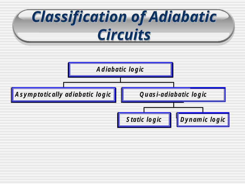
Classification of Adiabatic Circuits
Classification of Adiabatic Circuits
A sym p totically ad iaba tic lo g ic
S ta tic lo g ic D yn am ic lo g ic
Q u as i-adiaba tic lo g ic
A d iaba tic lo g ic
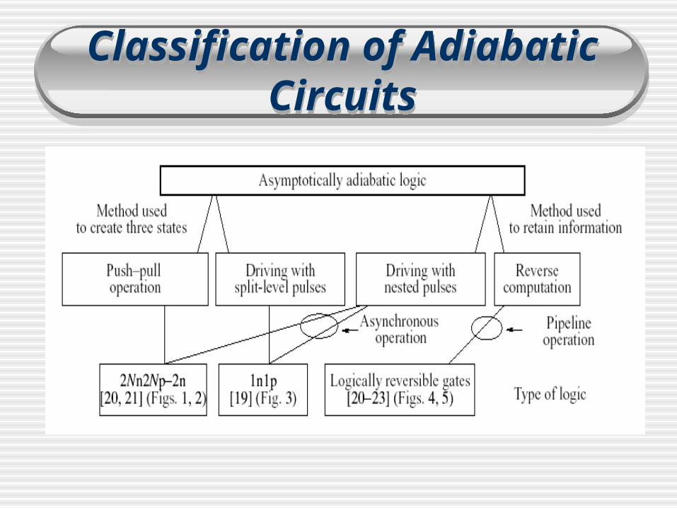
Classification of Adiabatic Circuits
Classification of Adiabatic Circuits
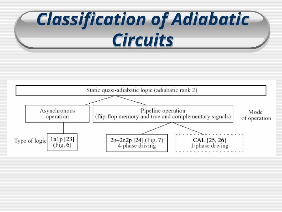
Classification of Adiabatic Circuits
Classification of Adiabatic Circuits
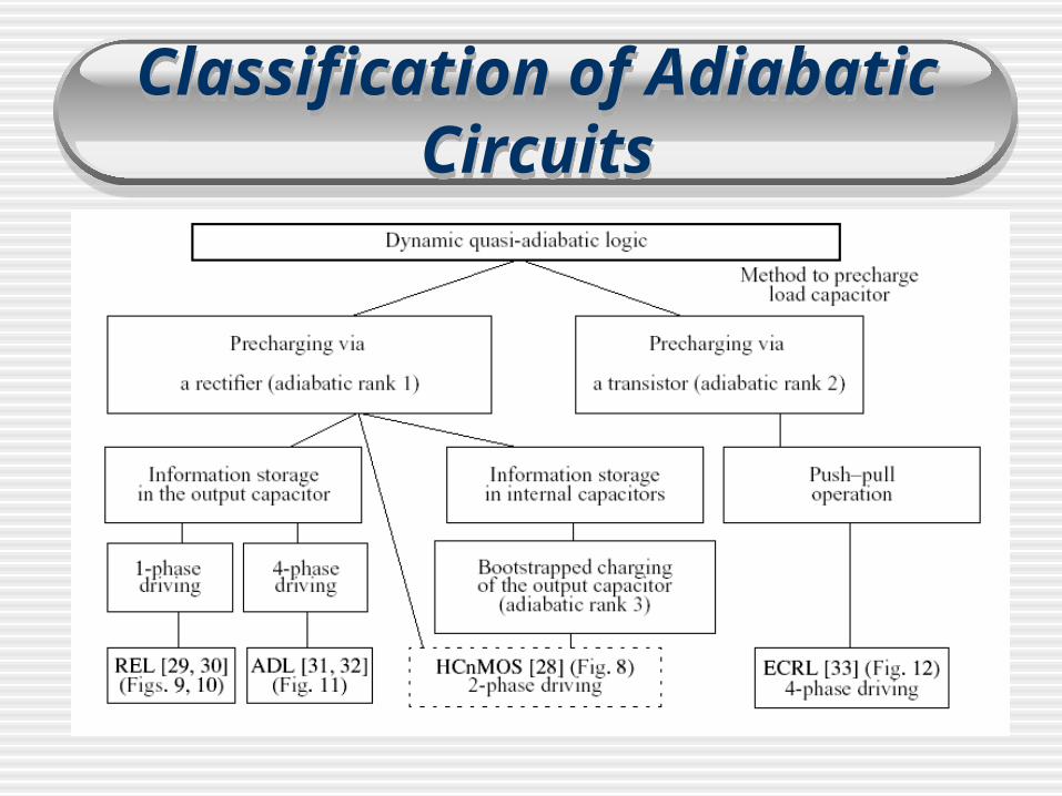
Classification of Adiabatic Circuits
Classification of Adiabatic Circuits
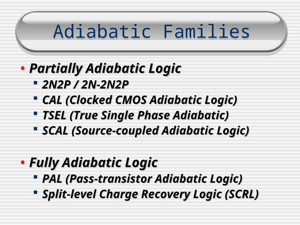
Adiabatic FamiliesAdiabatic Families
• Partially Adiabatic LogicPartially Adiabatic Logic 2N2P / 2N-2N2P 2N2P / 2N-2N2P CAL (Clocked CMOS Adiabatic Logic)CAL (Clocked CMOS Adiabatic Logic) TSEL (True Single Phase Adiabatic)TSEL (True Single Phase Adiabatic) SCAL (Source-coupled Adiabatic Logic)SCAL (Source-coupled Adiabatic Logic)
• Fully Adiabatic LogicFully Adiabatic Logic PAL (Pass-transistor Adiabatic Logic)PAL (Pass-transistor Adiabatic Logic) Split-level Charge Recovery Logic (SCRL)Split-level Charge Recovery Logic (SCRL)
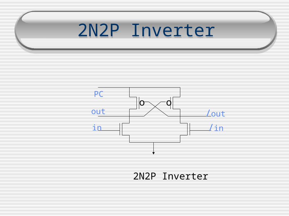
2N2P Inverter2N2P Inverter
2N2P Inverter
o oPC
out
in /in
/out
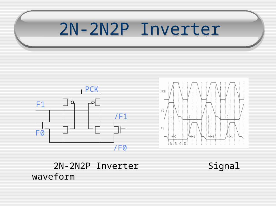
2N-2N2P Inverter2N-2N2P Inverter
2N-2N2P Inverter Signal waveform
o o
F1
F0 /F0
/F1
PCK
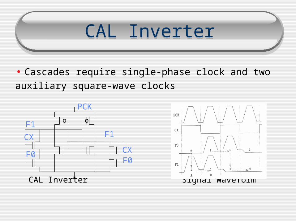
CAL InverterCAL Inverter
• Cascades require single-phase clock and two
auxiliary square-wave clocks
CAL Inverter Signal Waveform
o o
PCK
F1
CX
F0F0
F1
CX
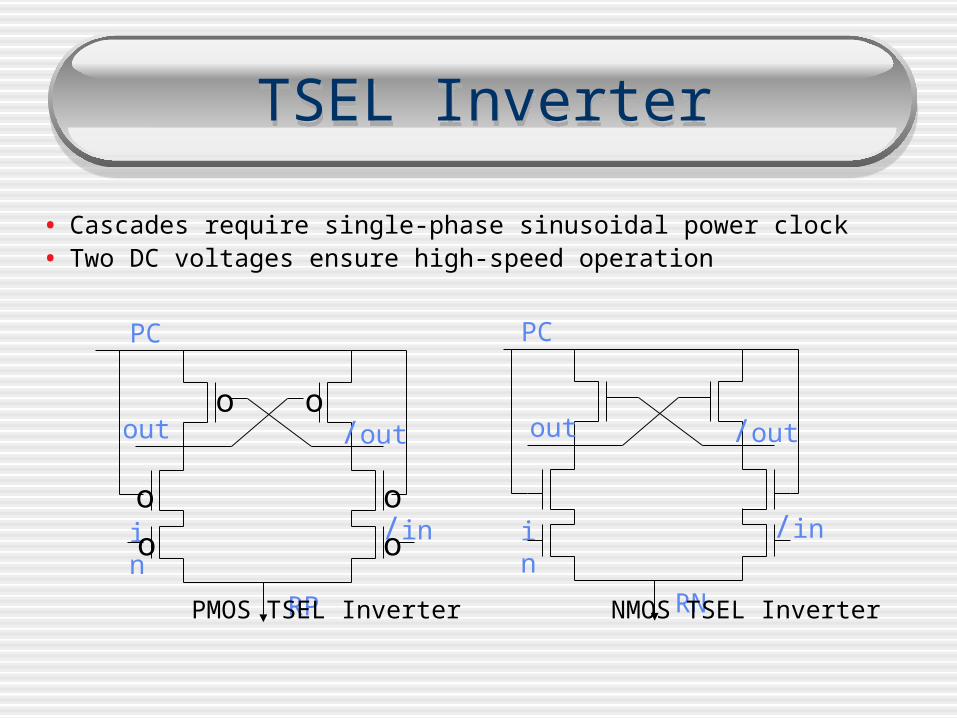
TSEL InverterTSEL Inverter
out
in /in
/out
PC
o oout
in /in
/out
PC
o o
o o
RP RN
• Cascades require single-phase sinusoidal power clock• Two DC voltages ensure high-speed operation
PMOS TSEL Inverter NMOS TSEL Inverter
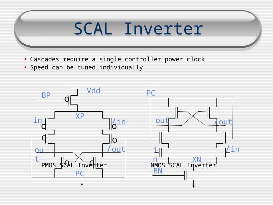
SCAL InverterSCAL Inverter
• Cascades require a single controller power clock• Speed can be tuned individually
PMOS SCAL Inverter NMOS SCAL Inverter
out
in /in
/out
PC BN
Vdd
o o
in /in
PC
out /out
o oo o
XP
XN
BP o
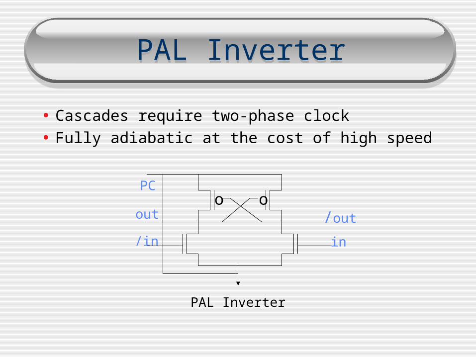
PAL InverterPAL Inverter
• Cascades require two-phase clock
• Fully adiabatic at the cost of high speed
PAL Inverter
o oPC
out
/in in
/out
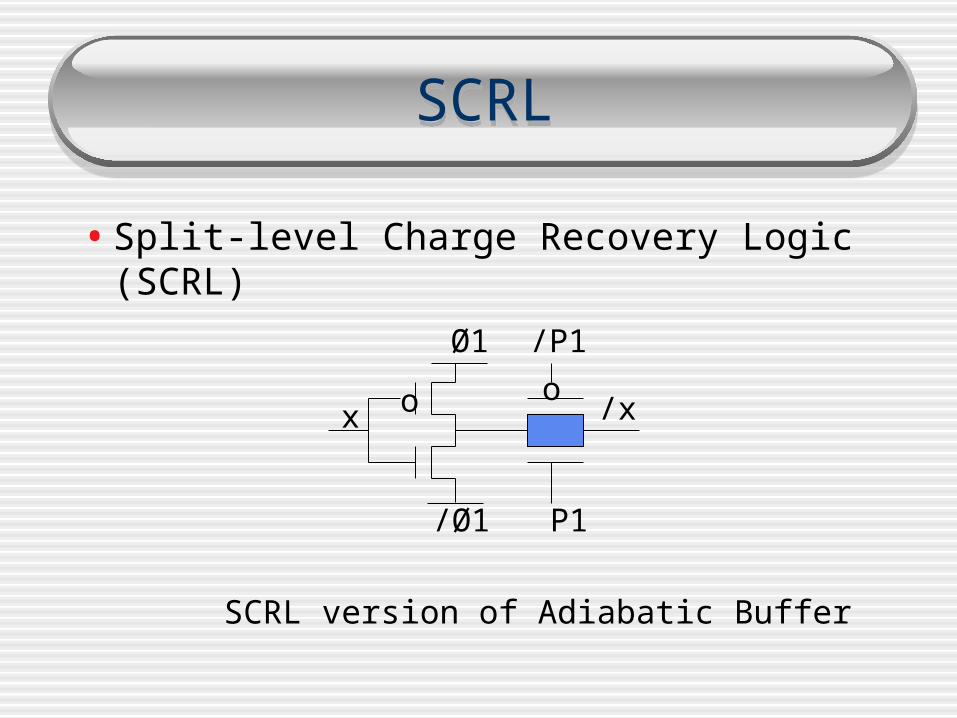
SCRLSCRL
• Split-level Charge Recovery Logic (SCRL)
SCRL version of Adiabatic Buffer
o o
/Ø1 P1
x /x
Ø1 /P1
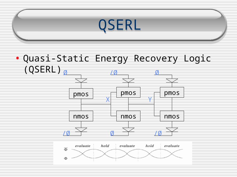
QSERLQSERL
• Quasi-Static Energy Recovery Logic (QSERL)
pmos
nmos nmos nmos
pmos pmos
Ø /Ø Ø
/Ø Ø /Ø
YX
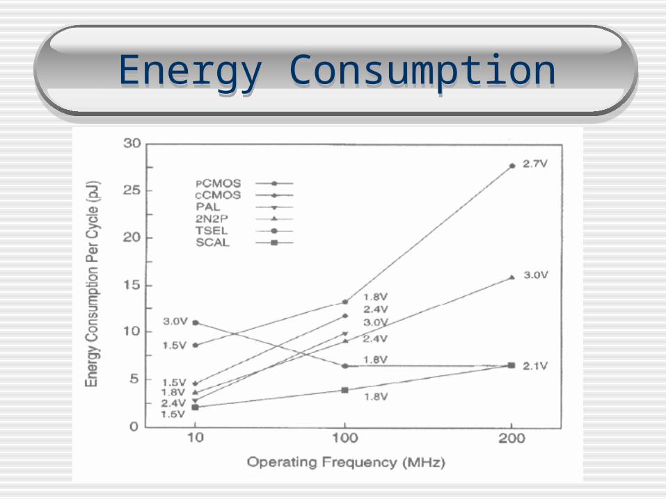
Energy ConsumptionEnergy Consumption
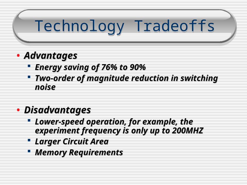
Technology TradeoffsTechnology Tradeoffs
• Advantages Advantages Energy saving of 76% to 90%Energy saving of 76% to 90% Two-order of magnitude reduction in switching Two-order of magnitude reduction in switching
noisenoise
• DisadvantagesDisadvantages Lower-speed operation, for example, the Lower-speed operation, for example, the
experiment frequency is only up to 200MHZexperiment frequency is only up to 200MHZ Larger Circuit AreaLarger Circuit Area Memory RequirementsMemory Requirements

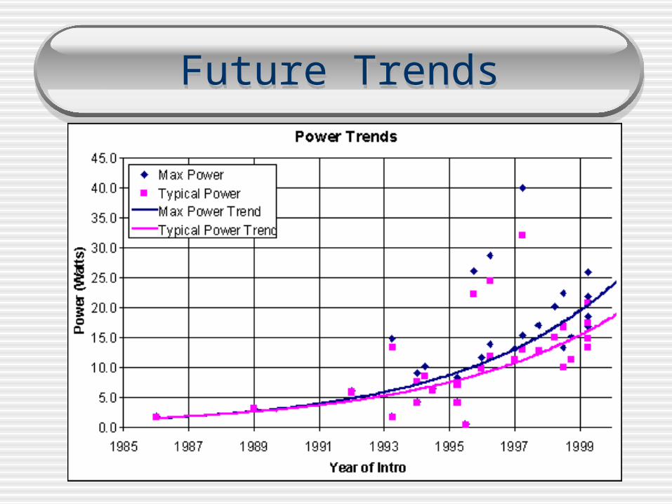
Future TrendsFuture Trends
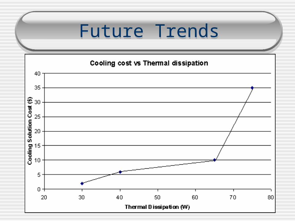
Future TrendsFuture Trends
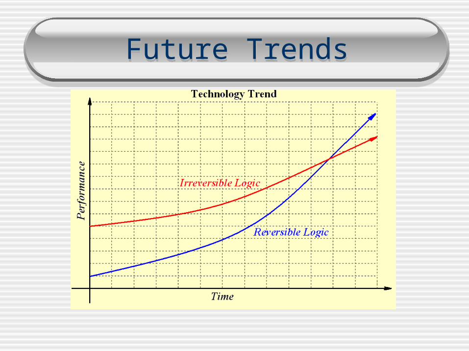
Future TrendsFuture Trends
Future TrendsFuture Trends
ContentsContents
IntroductionSignificanceBackground
DiscussionLiterature ReviewNumerical/Significant ResultsFuture Trends
Customized ProjectPlanTime Table
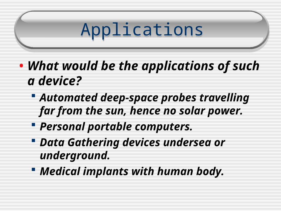
ApplicationsApplications
• What would be the applications of such a device? Automated deep-space probes travelling
far from the sun, hence no solar power. Personal portable computers. Data Gathering devices undersea or
underground. Medical implants with human body.
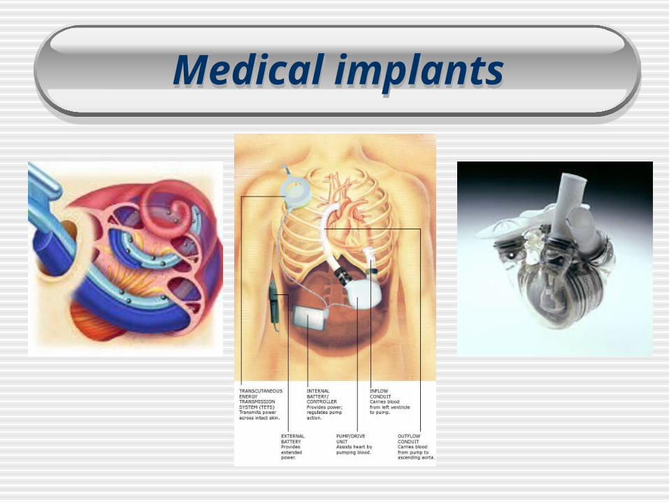
Medical implantsMedical implants
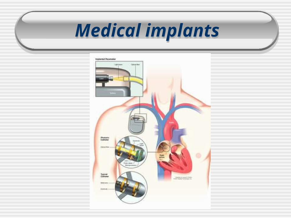
Medical implantsMedical implants
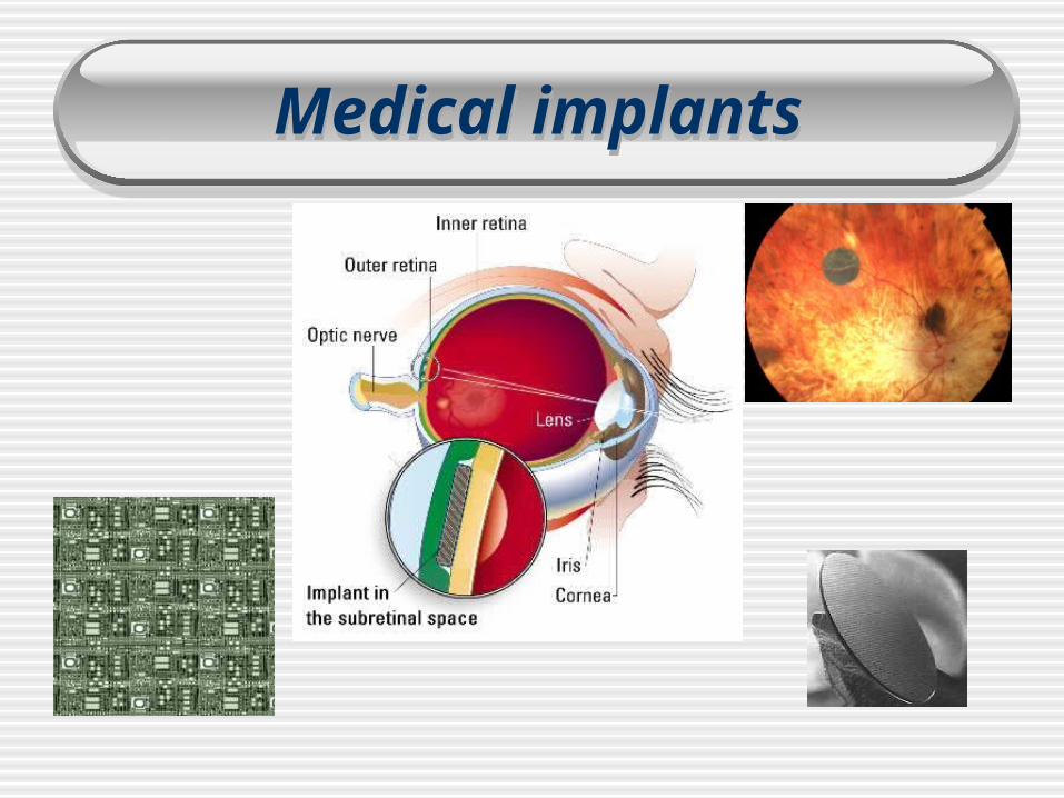
Medical implantsMedical implants
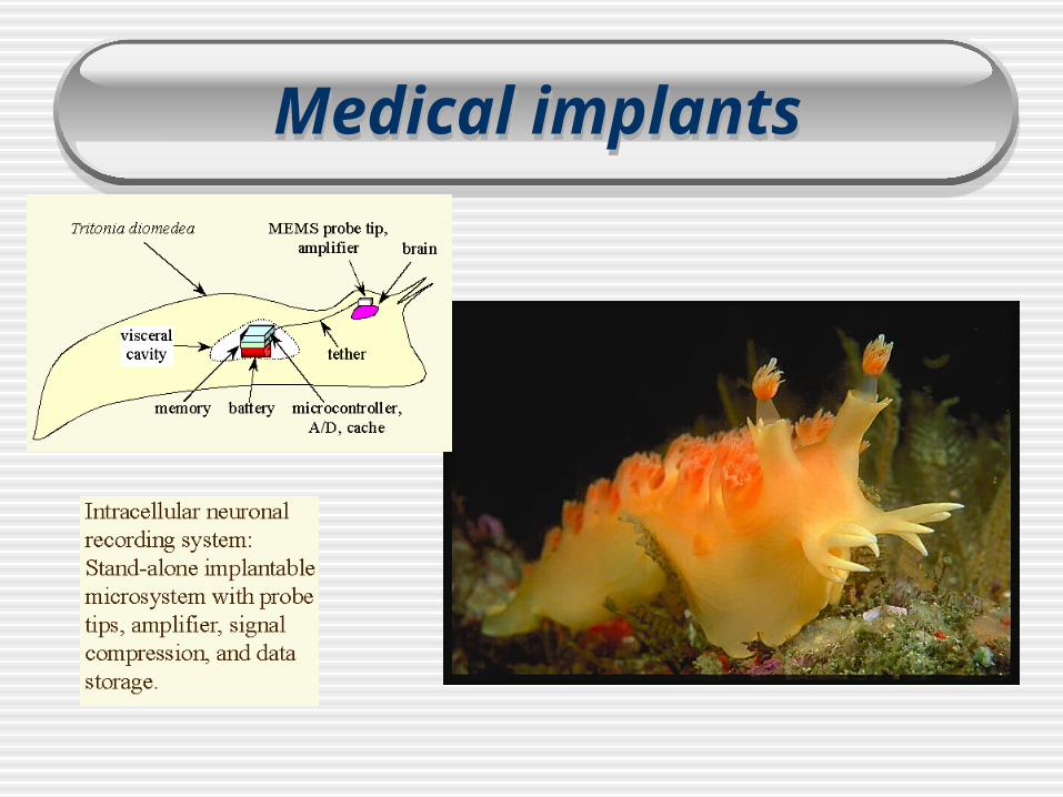
Medical implantsMedical implants
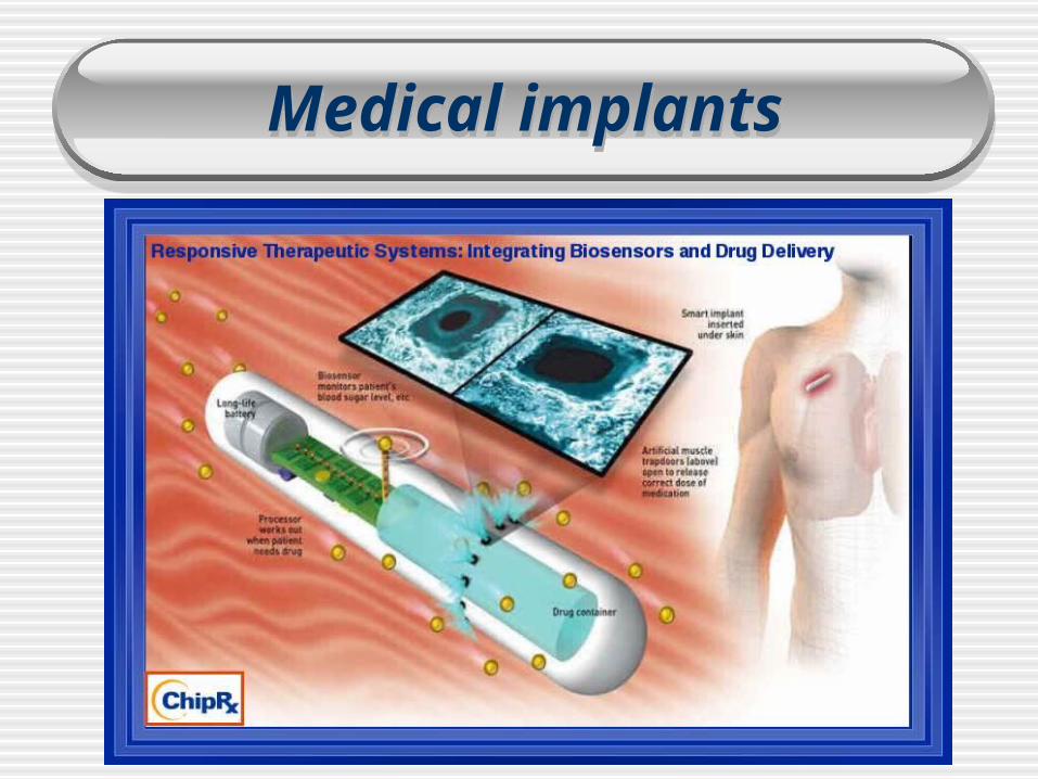
Medical implantsMedical implants
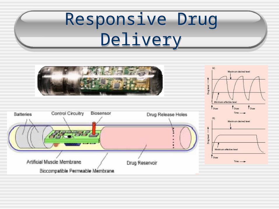
Responsive Drug DeliveryResponsive Drug Delivery
Low Power TechniquesLow Power Techniques
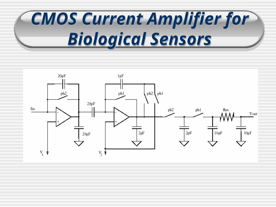
CMOS Current Amplifier for Biological Sensors
CMOS Current Amplifier for Biological Sensors
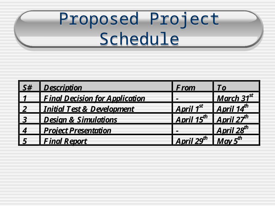
Proposed Project ScheduleProposed Project Schedule
S# Description From To1 Final Decision for Application - March 31st
2 Initial Test & Development April 1st April 14th
3 Design & Simulations April 15th April 27th
4 Project Presentation - April 28th
5 Final Report April 29th May 5th
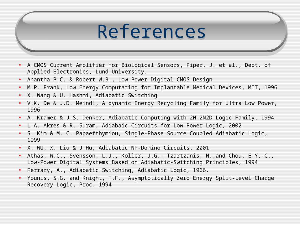
ReferencesReferences
• A CMOS Current Amplifier for Biological Sensors, Piper, J. et al., Dept. of Applied Electronics, Lund University.
• Anantha P.C. & Robert W.B., Low Power Digital CMOS Design
• M.P. Frank, Low Energy Computating for Implantable Medical Devices, MIT, 1996
• X. Wang & U. Hashmi, Adiabatic Switching
• V.K. De & J.D. Meindl, A dynamic Energy Recycling Family for Ultra Low Power, 1996
• A. Kramer & J.S. Denker, Adiabatic Computing with 2N-2N2D Logic Family, 1994
• L.A. Akres & R. Suram, Adiabaic Circuits for Low Power Logic, 2002
• S. Kim & M. C. Papaefthymiou, Single-Phase Source Coupled Adiabatic Logic, 1999
• X. WU, X. Liu & J Hu, Adiabatic NP-Domino Circuits, 2001
• Athas, W.C., Svensson, L.J., Koller, J.G., Tzartzanis, N.,and Chou, E.Y.-C., Low-Power Digital Systems Based on Adiabatic-Switching Principles, 1994
• Ferrary, A., Adiabatic Switching, Adiabatic Logic, 1966.
• Younis, S.G. and Knight, T.F., Asymptotically Zero Energy Split-Level Charge Recovery Logic, Proc. 1994

Thank You!Thank You!Thank You!Thank You!