
adc08d500 datasheet
48
ADC08D500 www.ti.com SNAS274F – MAY 2005 – REVISED APRIL 2013 ADC08D500 High Performance, Low Power, Dual 8-Bit, 500 MSPS A/D Converter Check for Samples: ADC08D500 1FEATURES DESCRIPTION The ADC08D500 is a dual, low power, high 2• Internal Sample-and-Hold performance CMOS analog-to-digital converter that • Single +1.9V ±0.1V Operation digitizes signals to 8 bits resolution at sampling rates • Choice of SDR or DDR Output Clocking up to 500 MSPS. Consuming a typical 1.4 Watts at 500 MSPS from a single 1.9 Volt supply, this device • Interleave Mode for 2x Sampling Rate is ensured to have no missing codes over the full • Multiple ADC Synchronization Capability operating temperature range. The unique folding and • Ensured No Missing Codes interpolating architecture, the fully differential comparator design, the innovative design of the • Serial Interface for Extended Control internal sample-and-hold amplifier and the self- • Fine Adjustment of Input Full-Scale Range and calibration scheme enable a very flat response of all Offset dynamic parameters beyond Nyquist, producing a • Duty Cycle Corrected Sample Clock high 7.5 ENOB with a 250 MHz input signal and a 500 MHz sample rate while providing a 10 -18 B.E.R. APPLICATIONS Output formatting is offset binary and the LVDS digital outputs are compatible with IEEE 1596.3-1996, • Direct RF Down Conversion with the exception of an adjustable common mode • Digital Oscilloscopes voltage between 0.8V and 1.2V. • Satellite Set-Top Boxes Each converter has a 1:2 demultiplexer that feeds • Communications Systems two LVDS buses and reduces the output data rate on each bus to half the sampling rate. The two • Test Instrumentation converters can be interleaved and used as a single 1 GSPS ADC. KEY SPECIFICATIONS The converter typically consumes less than 3.5 mW • Resolution 8 Bits in the Power Down Mode and is available in a 128- • Max Conversion Rate 500 MSPS (min) lead, thermally enhanced exposed pad HLQFP and • Bit Error Rate 10 -18 (typ) operates over the Industrial (-40°C ≤ T A ≤ +85°C) temperature range. • ENOB @ 250 MHz Input 7.5 Bits (typ) • DNL ±0.15 LSB (typ) • Power Consumption – Operating 1.4 W (typ) – Power Down Mode 3.5 mW (typ) 1 Please be aware that an important notice concerning availability, standard warranty, and use in critical applications of Texas Instruments semiconductor products and disclaimers thereto appears at the end of this data sheet. 2All trademarks are the property of their respective owners. PRODUCTION DATA information is current as of publication date. Copyright © 2005–2013, Texas Instruments Incorporated Products conform to specifications per the terms of the Texas Instruments standard warranty. Production processing does not necessarily include testing of all parameters.
description
adc08d500 datasheet
Transcript of adc08d500 datasheet
ADC08D500
www.ti.com SNAS274F –MAY 2005–REVISED APRIL 2013
ADC08D500 High Performance, Low Power, Dual 8-Bit, 500 MSPS A/D ConverterCheck for Samples: ADC08D500
1FEATURES DESCRIPTIONThe ADC08D500 is a dual, low power, high
2• Internal Sample-and-Holdperformance CMOS analog-to-digital converter that
• Single +1.9V ±0.1V Operation digitizes signals to 8 bits resolution at sampling rates• Choice of SDR or DDR Output Clocking up to 500 MSPS. Consuming a typical 1.4 Watts at
500 MSPS from a single 1.9 Volt supply, this device• Interleave Mode for 2x Sampling Rateis ensured to have no missing codes over the full• Multiple ADC Synchronization Capability operating temperature range. The unique folding and
• Ensured No Missing Codes interpolating architecture, the fully differentialcomparator design, the innovative design of the• Serial Interface for Extended Controlinternal sample-and-hold amplifier and the self-• Fine Adjustment of Input Full-Scale Range andcalibration scheme enable a very flat response of allOffset dynamic parameters beyond Nyquist, producing a
• Duty Cycle Corrected Sample Clock high 7.5 ENOB with a 250 MHz input signal and a500 MHz sample rate while providing a 10-18 B.E.R.
APPLICATIONS Output formatting is offset binary and the LVDSdigital outputs are compatible with IEEE 1596.3-1996,• Direct RF Down Conversionwith the exception of an adjustable common mode
• Digital Oscilloscopes voltage between 0.8V and 1.2V.• Satellite Set-Top Boxes Each converter has a 1:2 demultiplexer that feeds• Communications Systems two LVDS buses and reduces the output data rate on
each bus to half the sampling rate. The two• Test Instrumentationconverters can be interleaved and used as a single 1GSPS ADC.KEY SPECIFICATIONSThe converter typically consumes less than 3.5 mW• Resolution 8 Bitsin the Power Down Mode and is available in a 128-
• Max Conversion Rate 500 MSPS (min) lead, thermally enhanced exposed pad HLQFP and• Bit Error Rate 10-18 (typ) operates over the Industrial (-40°C ≤ TA ≤ +85°C)
temperature range.• ENOB @ 250 MHz Input 7.5 Bits (typ)• DNL ±0.15 LSB (typ)• Power Consumption
– Operating 1.4 W (typ)– Power Down Mode 3.5 mW (typ)
1
Please be aware that an important notice concerning availability, standard warranty, and use in critical applications ofTexas Instruments semiconductor products and disclaimers thereto appears at the end of this data sheet.
2All trademarks are the property of their respective owners.
PRODUCTION DATA information is current as of publication date. Copyright © 2005–2013, Texas Instruments IncorporatedProducts conform to specifications per the terms of the TexasInstruments standard warranty. Production processing does notnecessarily include testing of all parameters.
2
VREF
CLK/2
8-BITADC
VINI+
VINI-
DCLK+OutputClock
Generator DCLK-
Data Bus Output16 LVDS Pairs
DIOUT
DIOUTD
1:2 DEMUX& LATCH
ORControlLogic
I CHANNEL
8-BITADC
VINQ+
VINQ- Data Bus Output16 LVDS Pairs
DQOUT
DQOUTD
Q CHANNEL
3
CalRun
INPUTMUX
+
-
+
-
S/H
S/H
VBG
CLK+
CLK-
ControlInputs
SerialInterface
1:2 DEMUX& LATCH
ADC08D500
SNAS274F –MAY 2005–REVISED APRIL 2013 www.ti.com
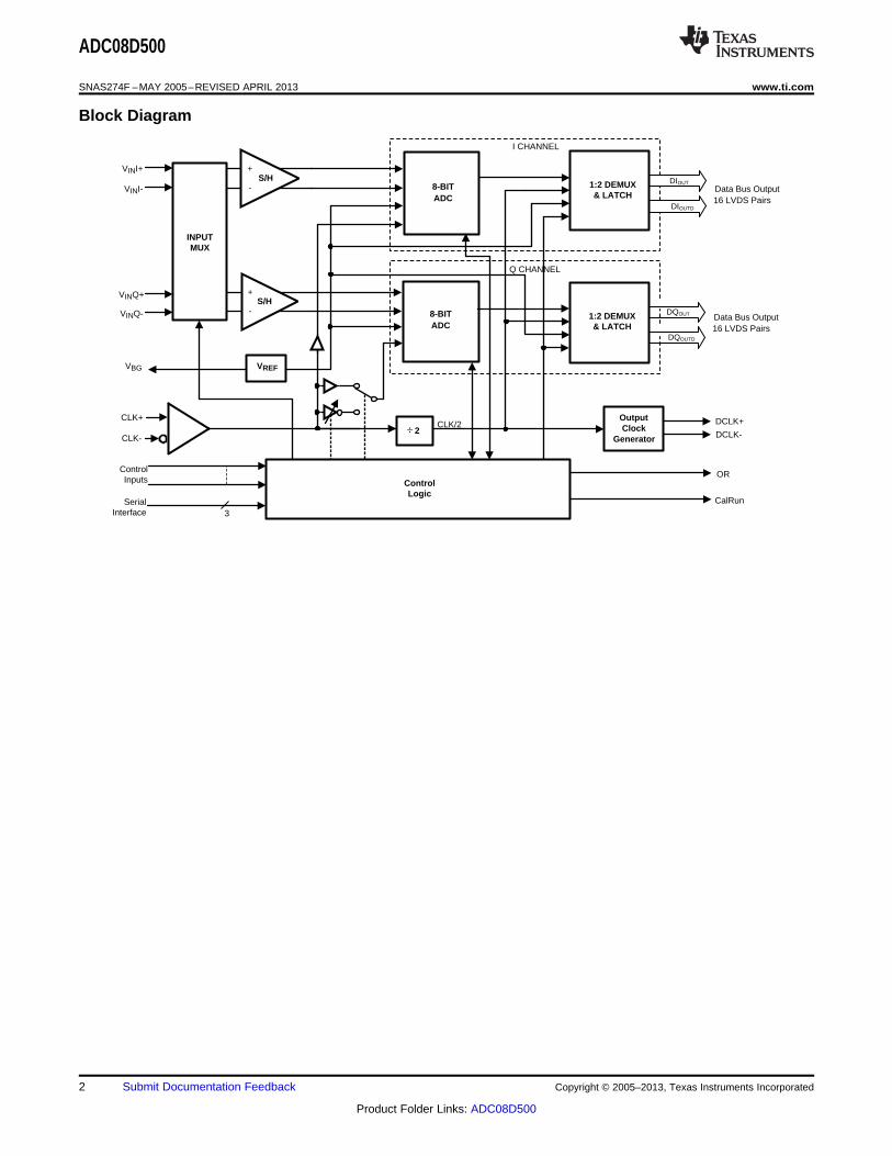
Block Diagram
2 Submit Documentation Feedback Copyright © 2005–2013, Texas Instruments Incorporated
Product Folder Links: ADC08D500
OutEdge/DDR/SDATAC
alD
ly/D
ES
/SC
S
GNDVA
OUTV/SCLK
VA
GNDVCMO
GNDVINI-VINI+
GNDD
R G
ND
12
16
DR
GN
D
FSR/ECE
CLK+CLK-
GNDVINQ+VINQ-GND
PDGND
ADC08D500
20
24
28
CALVBG
REXT
DR
GN
D
32313029
272625
232221
191817
151413
1110
1
4
89
765
32
Tdi
ode_
pT
diod
e_n
DQ
d0+
DQ
d0-
DQ
d1+
DQ
d1-
GN
DD
R G
ND
DQ
d2+
DQ
d2-
DQ
d3+
DQ
d3-
DQ
d4+
DQ
d4-
DQ
d5+
DQ
d5-
NC
37 41
DR
GN
DD
Qd6
+D
Qd6
-D
Qd7
+D
Qd7
-D
Q0+
DQ
0-D
Q1+
DQ
1-
NC
33 34 35 36 38 39 40 42 43 44 46 47 48 50 51 52 54 55 56 58 59 60 62 63 6445 49 53 57 61
DQ7+DQ7-OR+OR-DCLK-DCLK+DI7-DI7+DI6-DI6+DR GND
DI5-DI5+DI4-DI4+DI3-DI3+DI2-DI2+
71
81
86
91
96
DQ4+DQ4-DQ5+DQ5-
DR GNDDQ6+DQ6-
DQ2+DQ2-DQ3+DQ3-
76
6665
67686970
7372
7475
7877
7980
8382
8485
8887
8990
9392
9495
128
123
118
108
113
124
127
126
125
119
122
121
120
114
117
116
115
109
112
111
110
104
107
106
105 99
102
101
100
103 98 97
VA
VA
VA
PDQ
VA
VA
VA
VADCLK_RST
VA
VD
R
VD
R
VD
R
VDR
VDR
Cal
Run
DId
0+D
Id0-
DId
1+D
Id1-
VD
R
NC
DId
2+D
Id2-
DId
3+D
Id3-
DId
4+D
Id4-
DId
5+D
Id5-
NC
DId
6+D
Id6-
DId
7+D
Id7-
DI0
+D
I0-
DI1
+D
I1-
VD
R
NC
VD
R
VA
DR
GN
D
*
ADC08D500
www.ti.com SNAS274F –MAY 2005–REVISED APRIL 2013
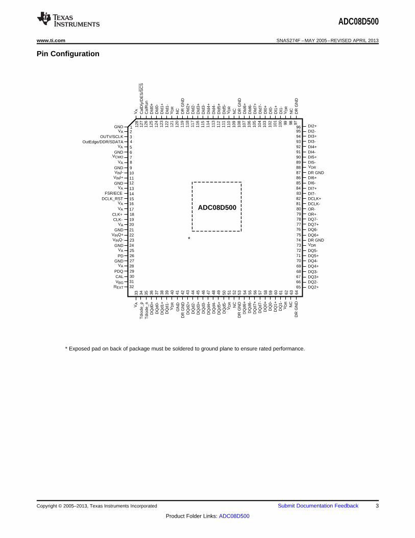
Pin Configuration
* Exposed pad on back of package must be soldered to ground plane to ensure rated performance.
Copyright © 2005–2013, Texas Instruments Incorporated Submit Documentation Feedback 3
Product Folder Links: ADC08D500
GND
VA
50k
50k
200k
8 pF
GND
VA
50 k:
GND
VA
GND
VA
50k
50k
200k
8 pF
VA
SDATA
DDR
GND
VA
50k
ADC08D500
SNAS274F –MAY 2005–REVISED APRIL 2013 www.ti.com
Pin Descriptions and Equivalent Circuits
Pin Functions
Pin No. Symbol Equivalent Circuit Description
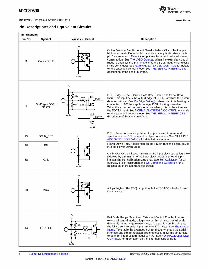
Output Voltage Amplitude and Serial Interface Clock. Tie this pinhigh for normal differential DCLK and data amplitude. Ground thispin for a reduced differential output amplitude and reduced powerconsumption. See The LVDS Outputs. When the extended control3 OutV / SCLK mode is enabled, this pin functions as the SCLK input which clocksin the serial data. See NORMAL/EXTENDED CONTROL for detailson the extended control mode. See THE SERIAL INTERFACE fordescription of the serial interface.
DCLK Edge Select, Double Data Rate Enable and Serial DataInput. This input sets the output edge of DCLK+ at which the outputdata transitions. (See OutEdge Setting). When this pin is floating or
OutEdge / DDR / connected to 1/2 the supply voltage, DDR clocking is enabled.4 SDATA When the extended control mode is enabled, this pin functions asthe SDATA input. See NORMAL/EXTENDED CONTROL for detailson the extended control mode. See THE SERIAL INTERFACE fordescription of the serial interface.
DCLK Reset. A positive pulse on this pin is used to reset and15 DCLK_RST synchronize the DCLK outs of multiple converters. See MULTIPLE
ADC SYNCHRONIZATION for detailed description.
Power Down Pins. A logic high on the PD pin puts the entire device26 PD into the Power Down Mode.
Calibration Cycle Initiate. A minimum 80 input clock cycles logic lowfollowed by a minimum of 80 input clock cycles high on this pin
30 CAL initiates the self calibration sequence. See Self Calibration for anoverview of self-calibration and On-Command Calibration for adescription of on-command calibration.
A logic high on the PDQ pin puts only the "Q" ADC into the Power29 PDQ Down mode.
Full Scale Range Select and Extended Control Enable. In non-extended control mode, a logic low on this pin sets the full-scaledifferential input range to 650 mVP-P. A logic high on this pin setsthe full-scale differential input range to 870 mVP-P. See The Analog14 FSR/ECE Inputs. To enable the extended control mode, whereby the serialinterface and control registers are employed, allow this pin to floator connect it to a voltage equal to VA/2. See NORMAL/EXTENDEDCONTROL for information on the extended control mode.
4 Submit Documentation Feedback Copyright © 2005–2013, Texas Instruments Incorporated
Product Folder Links: ADC08D500
VD
DGND
GND
VA
200k
8 pF
VCM
Enable AC Coupling
50k
VA
AGND
VA
AGND
50k
Control from VCMO
VCMO
100
VA
AGND
VA
AGND
100 VBIAS
50k
50k
GND
VA
50k
50k
ADC08D500
www.ti.com SNAS274F –MAY 2005–REVISED APRIL 2013
Pin Functions
Pin No. Symbol Equivalent Circuit Description
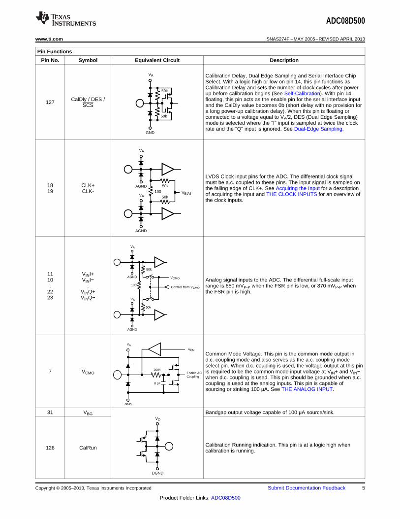
Calibration Delay, Dual Edge Sampling and Serial Interface ChipSelect. With a logic high or low on pin 14, this pin functions asCalibration Delay and sets the number of clock cycles after powerup before calibration begins (See Self-Calibration). With pin 14
CalDly / DES / floating, this pin acts as the enable pin for the serial interface input127 SCS and the CalDly value becomes 0b (short delay with no provision fora long power-up calibration delay). When this pin is floating orconnected to a voltage equal to VA/2, DES (Dual Edge Sampling)mode is selected where the "I" input is sampled at twice the clockrate and the "Q" input is ignored. See Dual-Edge Sampling.
LVDS Clock input pins for the ADC. The differential clock signalmust be a.c. coupled to these pins. The input signal is sampled on18 CLK+ the falling edge of CLK+. See Acquiring the Input for a description19 CLK- of acquiring the input and THE CLOCK INPUTS for an overview ofthe clock inputs.
11 VINI+10 VINI− Analog signal inputs to the ADC. The differential full-scale input. . range is 650 mVP-P when the FSR pin is low, or 870 mVP-P when
22 VINQ+ the FSR pin is high.23 VINQ−
Common Mode Voltage. This pin is the common mode output ind.c. coupling mode and also serves as the a.c. coupling modeselect pin. When d.c. coupling is used, the voltage output at this pin
7 VCMO is required to be the common mode input voltage at VIN+ and VIN−when d.c. coupling is used. This pin should be grounded when a.c.coupling is used at the analog inputs. This pin is capable ofsourcing or sinking 100 μA. See THE ANALOG INPUT.
31 VBG Bandgap output voltage capable of 100 μA source/sink.
Calibration Running indication. This pin is at a logic high when126 CalRun calibration is running.
Copyright © 2005–2013, Texas Instruments Incorporated Submit Documentation Feedback 5
Product Folder Links: ADC08D500

VDR
DR GND
+
-+
-
Tdiode_P
Tdiode_N
V
VA
GND
ADC08D500
SNAS274F –MAY 2005–REVISED APRIL 2013 www.ti.com
Pin Functions
Pin No. Symbol Equivalent Circuit Description
External bias resistor connection. Nominal value is 3.3k-Ohms32 REXT (±0.1%) to ground. See Self-Calibration.
Temperature Diode Positive (Anode) and Negative (Cathode).These pins may be used for die temperature measurements,
34 Tdiode_P however no specified accuracy is implied or ensured. Noise35 Tdiode_N coupling from adjacent output data signals has been shown to
affect temperature measurements using this feature. See ThermalManagement.
83 / 78 DI7− / DQ7−84 / 77 DI7+ / DQ7+85 / 76 DI6− / DQ6−86 / 75 DI6+ / DQ6+89 / 72 DI5− / DQ5−90 / 71 DI5+ / DQ5+91 / 70 DI4− / DQ4− I and Q channel LVDS Data Outputs that are not delayed in the92 / 69 DI4+ / DQ4+ output demultiplexer. Compared with the DId and DQd outputs,93 / 68 DI3− / DQ3− these outputs represent the later time samples. These outputs94 / 67 DI3+ / DQ3+ should always be terminated with a 100Ω differential resistor.95 / 66 DI2− / DQ2−96 / 65 DI2+ / DQ2+100 / 61 DI1− / DQ1−101 / 60 DI1+ / DQ1+102 / 59 DI0− / DQ0−103 / 58 DI0+ / DQ0+
104 / 57 DId7− / DQd7−105 / 56 DId7+ / DQd7+106 / 55 DId6− / DQd6−107 / 54 DId6+ / DQd6+111 / 50 DId5− / DQd5−112 / 49 DId5+ / DQd5+ I and Q channel LVDS Data Outputs that are delayed by one CLK113 / 48 DId4− / DQd4− cycle in the output demultiplexer. Compared with the DI/DQ114 / 47 DId4+ / DQd4+ outputs, these outputs represent the earlier time sample. These115 / 46 DId3− / DQd3− outputs should always be terminated with a 100Ω differential116 / 45 DId3+ / DQd3+ resistor.117 / 44 DId2− / DQd2−118 / 43 DId2+ / DQd2+122 / 39 DId1− / DQd1−123 / 38 DId1+ / DQd1+124 / 37 DId0− / DQd0−125 / 36 DId0+ / DQd0+
Out Of Range output. A differential high at these pins indicates that79 OR+ the differential input is out of range (outside the range ±325 mV or80 OR- ±435 mV as defined by the FSR pin).
Differential Clock outputs used to latch the output data. Delayedand non-delayed data outputs are supplied synchronous to this
82 DCLK+ signal. This signal is at 1/2 the input clock rate in SDR mode and at81 DCLK- 1/4 the input clock rate in the DDR mode. The DCLK outputs are
not active during a calibration cycle, therefore this is notrecommended as a system clock.
2, 5, 8, 13,16, 17, 20, VA Analog power supply pins. Bypass these pins to ground.25, 28, 33,
128
6 Submit Documentation Feedback Copyright © 2005–2013, Texas Instruments Incorporated
Product Folder Links: ADC08D500
ADC08D500
www.ti.com SNAS274F –MAY 2005–REVISED APRIL 2013
Pin Functions
Pin No. Symbol Equivalent Circuit Description
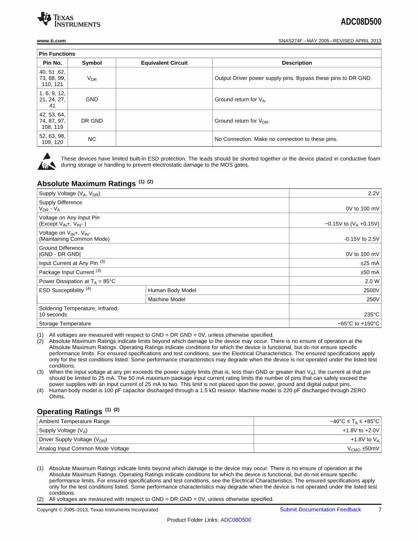
40, 51 ,62,73, 88, 99, VDR Output Driver power supply pins. Bypass these pins to DR GND.110, 121
1, 6, 9, 12,21, 24, 27, GND Ground return for VA.
41
42, 53, 64,74, 87, 97, DR GND Ground return for VDR.108, 119
52, 63, 98, NC No Connection. Make no connection to these pins.109, 120
These devices have limited built-in ESD protection. The leads should be shorted together or the device placed in conductive foamduring storage or handling to prevent electrostatic damage to the MOS gates.
Absolute Maximum Ratings (1) (2)
Supply Voltage (VA, VDR) 2.2V
Supply DifferenceVDR - VA 0V to 100 mV
Voltage on Any Input Pin(Except VIN+, VIN- ) −0.15V to (VA +0.15V)
Voltage on VIN+, VIN-(Maintaining Common Mode) -0.15V to 2.5V
Ground Difference|GND - DR GND| 0V to 100 mV
Input Current at Any Pin (3) ±25 mA
Package Input Current (3) ±50 mA
Power Dissipation at TA = 85°C 2.0 W
ESD Susceptibility (4) Human Body Model 2500V
Machine Model 250V
Soldering Temperature, Infrared,10 seconds 235°C
Storage Temperature −65°C to +150°C
(1) All voltages are measured with respect to GND = DR GND = 0V, unless otherwise specified.(2) Absolute Maximum Ratings indicate limits beyond which damage to the device may occur. There is no ensure of operation at the
Absolute Maximum Ratings. Operating Ratings indicate conditions for which the device is functional, but do not ensure specificperformance limits. For ensured specifications and test conditions, see the Electrical Characteristics. The ensured specifications applyonly for the test conditions listed. Some performance characteristics may degrade when the device is not operated under the listed testconditions.
(3) When the input voltage at any pin exceeds the power supply limits (that is, less than GND or greater than VA), the current at that pinshould be limited to 25 mA. The 50 mA maximum package input current rating limits the number of pins that can safely exceed thepower supplies with an input current of 25 mA to two. This limit is not placed upon the power, ground and digital output pins.
(4) Human body model is 100 pF capacitor discharged through a 1.5 kΩ resistor. Machine model is 220 pF discharged through ZEROOhms.
Operating Ratings (1) (2)
Ambient Temperature Range −40°C ≤ TA ≤ +85°C
Supply Voltage (VA) +1.8V to +2.0V
Driver Supply Voltage (VDR) +1.8V to VA
Analog Input Common Mode Voltage VCMO ±50mV
(1) Absolute Maximum Ratings indicate limits beyond which damage to the device may occur. There is no ensure of operation at theAbsolute Maximum Ratings. Operating Ratings indicate conditions for which the device is functional, but do not ensure specificperformance limits. For ensured specifications and test conditions, see the Electrical Characteristics. The ensured specifications applyonly for the test conditions listed. Some performance characteristics may degrade when the device is not operated under the listed testconditions.
(2) All voltages are measured with respect to GND = DR GND = 0V, unless otherwise specified.
Copyright © 2005–2013, Texas Instruments Incorporated Submit Documentation Feedback 7
Product Folder Links: ADC08D500

I / O
GND
VA
TO INTERNALCIRCUITRY
ADC08D500
SNAS274F –MAY 2005–REVISED APRIL 2013 www.ti.com
Operating Ratings (1) (2) (continued)VIN+, VIN- Voltage Range (Maintaining Common Mode) 0V to 2.15V
(100% duty cycle)0V to 2.5V
(10% duty cycle)
Ground Difference 0V(|GND - DR GND|)
CLK Pins Voltage Range 0V to VA
Differential CLK Amplitude 0.4VP-P to 2.0VP-P
Package Thermal Resistance (1)
Package θJA θJC (Top of Package) θJ-PAD (Thermal Pad)
128-Lead Exposed Pad 25°C / W 10°C / W 2.8°C / WHLQFP
(1) Soldering process must comply with TI’s Reflow Temperature Profile specifications. Refer to www.ti.com/packaging.
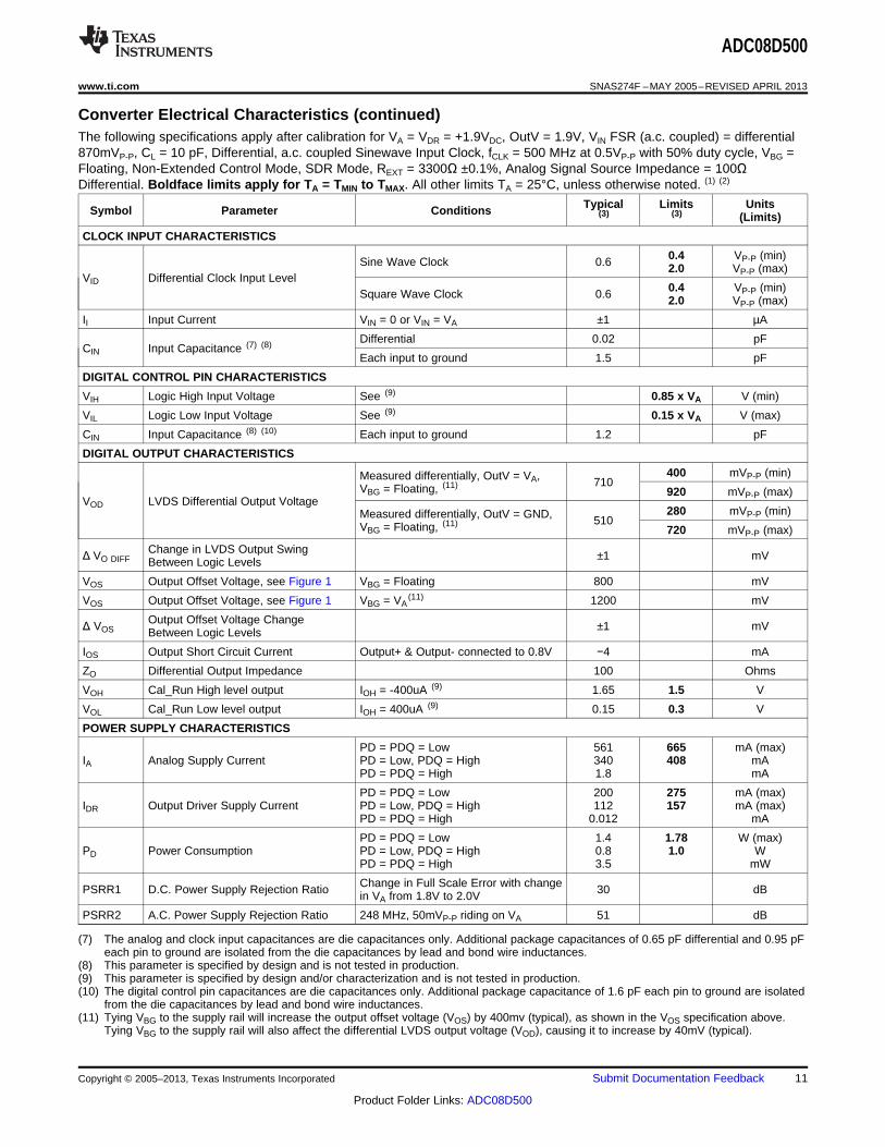
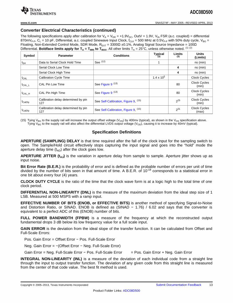
Converter Electrical CharacteristicsThe following specifications apply after calibration for VA = VDR = +1.9VDC, OutV = 1.9V, VIN FSR (a.c. coupled) = differential870mVP-P, CL = 10 pF, Differential, a.c. coupled Sinewave Input Clock, fCLK = 500 MHz at 0.5VP-P with 50% duty cycle, VBG =Floating, Non-Extended Control Mode, SDR Mode, REXT = 3300Ω ±0.1%, Analog Signal Source Impedance = 100ΩDifferential. Boldface limits apply for TA = TMIN to TMAX. All other limits TA = 25°C, unless otherwise noted. (1) (2)
Typical Limits UnitsSymbol Parameter Conditions (3) (3) (Limits)
STATIC CONVERTER CHARACTERISTICS
DC Coupled, 1MHz Sine Wave OverINL Integral Non-Linearity ±0.3 ±0.9 LSB (max)ranged
DC Coupled, 1MHz Sine Wave OverDNL Differential Non-Linearity ±0.15 ±0.6 LSB (max)ranged
Resolution with No Missing Codes 8 Bits
−1.5 LSB (min)VOFF Offset Error -0.45 0.5 LSB (max)
VOFF_ADJ Input Offset Adjustment Range Extended Control Mode ±45 mV
PFSE Positive Full-Scale Error (4) −0.6 ±25 mV (max)
NFSE Negative Full-Scale Error (4) −1.31 ±25 mV (max)
FS_ADJ Full-Scale Adjustment Range Extended Control Mode ±20 ±15 %FS
NORMAL MODE (non DES) DYNAMIC CONVERTER CHARACTERISTICS
FPBW Full Power Bandwidth Normal (non DES) Mode 1.7 GHz
(1) The analog inputs are protected as shown below. Input voltage magnitudes beyond the Absolute Maximum Ratings may damage thisdevice.
(2) To ensure accuracy, it is required that VA and VDR be well bypassed. Each supply pin must be decoupled with separate bypasscapacitors. Additionally, achieving rated performance requires that the backside exposed pad be well grounded.
(3) Typical figures are at TA = 25°C, and represent most likely parametric norms. Test limits are specified to TI's AOQL (Average OutgoingQuality Level).
(4) Calculation of Full-Scale Error for this device assumes that the actual reference voltage is exactly its nominal value. Full-Scale Error forthis device, therefore, is a combination of Full-Scale Error and Reference Voltage Error. See Figure 2. For relationship between GainError and Full-Scale Error, see Specification Definitions for Gain Error.
8 Submit Documentation Feedback Copyright © 2005–2013, Texas Instruments Incorporated
Product Folder Links: ADC08D500

ADC08D500
www.ti.com SNAS274F –MAY 2005–REVISED APRIL 2013
Converter Electrical Characteristics (continued)The following specifications apply after calibration for VA = VDR = +1.9VDC, OutV = 1.9V, VIN FSR (a.c. coupled) = differential870mVP-P, CL = 10 pF, Differential, a.c. coupled Sinewave Input Clock, fCLK = 500 MHz at 0.5VP-P with 50% duty cycle, VBG =Floating, Non-Extended Control Mode, SDR Mode, REXT = 3300Ω ±0.1%, Analog Signal Source Impedance = 100ΩDifferential. Boldface limits apply for TA = TMIN to TMAX. All other limits TA = 25°C, unless otherwise noted. (1) (2)
Typical Limits UnitsSymbol Parameter Conditions (3) (3) (Limits)
B.E.R. Bit Error Rate 10-18 Error/Sample
Gain Flatness d.c. to 500 MHz ±0.5 dBFS
fIN = 50 MHz, VIN = FSR − 0.5 dB 7.5 Bits
ENOB Effective Number of Bits fIN = 100 MHz, VIN = FSR − 0.5 dB 7.5 7.1 Bits (min)
fIN = 248 MHz, VIN = FSR − 0.5 dB 7.5 7.1 Bits (min)
fIN = 50 MHz, VIN = FSR − 0.5 dB 47 dB
SINAD Signal-to-Noise Plus Distortion Ratio fIN = 100 MHz, VIN = FSR − 0.5 dB 47 44.5 dB (min)
fIN = 248 MHz, VIN = FSR − 0.5 dB 47 44.5 dB (min)
fIN = 50 MHz, VIN = FSR − 0.5 dB 48 dB
SNR Signal-to-Noise Ratio fIN = 100 MHz, VIN = FSR − 0.5 dB 48 45.3 dB (min)
fIN = 248 MHz, VIN = FSR − 0.5 dB 47.5 45.3 dB (min)
fIN = 50 MHz, VIN = FSR − 0.5 dB -55 dB
THD Total Harmonic Distortion fIN = 100 MHz, VIN = FSR − 0.5 dB -55 −47.5 dB (max)
fIN = 248 MHz, VIN = FSR − 0.5 dB -55 −47.5 dB (max)
fIN = 50 MHz, VIN = FSR − 0.5 dB −60 dB
2nd Harm Second Harmonic Distortion fIN = 100 MHz, VIN = FSR − 0.5 dB −60 dB
fIN = 248 MHz, VIN = FSR − 0.5 dB −60 dB
fIN = 50 MHz, VIN = FSR − 0.5 dB −65 dB
3rd Harm Third Harmonic Distortion fIN = 100 MHz, VIN = FSR − 0.5 dB −65 dB
fIN = 248 MHz, VIN = FSR − 0.5 dB −65 dB
fIN = 50 MHz, VIN = FSR − 0.5 dB 55 dB
SFDR Spurious-Free dynamic Range fIN = 100 MHz, VIN = FSR − 0.5 dB 55 47.5 dB (min)
fIN = 248 MHz, VIN = FSR − 0.5 dB 55 47.5 dB (min)
fIN1 = 121 MHz, VIN = FSR − 7 dBIMD Intermodulation Distortion -50 dBfIN2 = 126 MHz, VIN = FSR − 7 dB
(VIN+) − (VIN−) > + Full Scale 255Out of Range Output Code(In addition to OR Output high) (VIN+) − (VIN−) < − Full Scale 0
INTERLEAVE MODE (DES Pin 127=Float) - DYNAMIC CONVERTER CHARACTERISTICS
FPBW Full Power Bandwidth Dual Edge Sampling Mode 900 MHz(DES)
fIN = 100 MHz, VIN = FSR − 0.5 dB 7.4 7.0 Bits (min)ENOB Effective Number of Bits
fIN = 248 MHz, VIN = FSR − 0.5 dB 7.4 7.0 Bits (min)
fIN = 100 MHz, VIN = FSR − 0.5 dB 46.3 43.9 dB (min)SINAD Signal to Noise Plus Distortion Ratio
fIN = 248 MHz, VIN = FSR − 0.5 dB 46.3 43.9 dB (min)
fIN = 100 MHz, VIN = FSR − 0.5 dB 46.7 44.1 dB (min)SNR Signal to Noise Ratio
fIN = 248 MHz, VIN = FSR − 0.5 dB 46.7 44.1 dB (min)
fIN = 100 MHz, VIN = FSR − 0.5 dB -58 -49 dB (min)THD Total Harmonic Distortion
fIN = 248 MHz, VIN = FSR − 0.5 dB -58 -49 dB (min)
fIN = 100 MHz, VIN = FSR − 0.5 dB -60 dB2nd Harm Second Harmonic Distortion
fIN = 248 MHz, VIN = FSR − 0.5 dB -60 dB
fIN = 100 MHz, VIN = FSR − 0.5 dB -64 dB3rd Harm Third Harmonic Distortion
fIN = 248 MHz, VIN = FSR − 0.5 dB -64 dB
fIN = 248 MHz, VIN = FSR − 0.5 dB 57 47 dB(min)SFDR Spurious Free Dynamic Range
fIN = 248 MHz, VIN = FSR − 0.5 dB 57 47 dB dB (min(min)
Copyright © 2005–2013, Texas Instruments Incorporated Submit Documentation Feedback 9
Product Folder Links: ADC08D500

ADC08D500
SNAS274F –MAY 2005–REVISED APRIL 2013 www.ti.com
Converter Electrical Characteristics (continued)The following specifications apply after calibration for VA = VDR = +1.9VDC, OutV = 1.9V, VIN FSR (a.c. coupled) = differential870mVP-P, CL = 10 pF, Differential, a.c. coupled Sinewave Input Clock, fCLK = 500 MHz at 0.5VP-P with 50% duty cycle, VBG =Floating, Non-Extended Control Mode, SDR Mode, REXT = 3300Ω ±0.1%, Analog Signal Source Impedance = 100ΩDifferential. Boldface limits apply for TA = TMIN to TMAX. All other limits TA = 25°C, unless otherwise noted. (1) (2)
Typical Limits UnitsSymbol Parameter Conditions (3) (3) (Limits)
ANALOG INPUT AND REFERENCE CHARACTERISTICS
570 mVP-P (min)FSR pin 14 Low 650
730 mVP-P (max)Full Scale Analog Differential InputVIN Range 790 mVP-P (min)FSR pin 14 High 870
950 mVP-P (max)
VCMO − 50 mV (min)VCMI Analog Input Common Mode Voltage VCMO VCMO + 50 mV (max)
Differential 0.02 pFAnalog Input Capacitance, Normaloperation (5) (6)
Each input pin to ground 1.6 pFCIN
Differential 0.08 pFAnalog Input Capacitance, DES Mode(5) (6)
Each input pin to ground 2.2 pF
94 Ω (min)RIN Differential Input Resistance 100
106 Ω (max)
ANALOG OUTPUT CHARACTERISTICS
0.95 V (min)VCMO Common Mode Output Voltage 1.26 1.45 V (max)
VA = 1.8V 0.60 VVCMO input threshold to set DCVCMO_LVL Coupling mode VA = 2.0V 0.66 V
Common Mode Output VoltageTC VCMO TA = −40°C to +85°C 118 ppm/°CTemperature Coefficient
CLOAD Maximum VCMO load Capacitance 80 pFVCMO
1.20 V (min)VBG Bandgap Reference Output Voltage IBG = ±100 µA 1.26 1.33 V (max)
Bandgap Reference VoltageTC VBG TA = −40°C to +85°C, IBG = ±100 µA 28 ppm/°CTemperature Coefficient
Maximum Bandgap Reference LoadCLOAD VBG 80 pFCapacitance
TEMPERATURE DIODE CHARACTERISTICS
192 µA vs. 12 µA, 71.23 mVTJ = 25°CΔVBE Temperature Diode Voltage
192 µA vs. 12 µA, 85.54 mVTJ = 85°C
CHANNEL-TO-CHANNEL CHARACTERISTICS
Offset Error Match 1 LSB
Positive Full-Scale Error Match Zero offset selected in Control Register 1 LSB
Negative Full-Scale Error Match Zero offset selected in Control Register 1 LSB
Phase Matching (I, Q) FIN = 1.0 GHz < 1 Degree
Crosstalk from I (Aggressor) to Q Aggressor = 867 MHz F.S.X-TALK −71 dB(Victim) Channel Victim = 100 MHz F.S.
Crosstalk from Q (Aggressor) to I Aggressor = 867 MHz F.S.X-TALK -71 dB(Victim) Channel Victim = 100 MHz F.S.
(5) The analog and clock input capacitances are die capacitances only. Additional package capacitances of 0.65 pF differential and 0.95 pFeach pin to ground are isolated from the die capacitances by lead and bond wire inductances.
(6) This parameter is specified by design and is not tested in production.
10 Submit Documentation Feedback Copyright © 2005–2013, Texas Instruments Incorporated
Product Folder Links: ADC08D500
ADC08D500
www.ti.com SNAS274F –MAY 2005–REVISED APRIL 2013
Converter Electrical Characteristics (continued)The following specifications apply after calibration for VA = VDR = +1.9VDC, OutV = 1.9V, VIN FSR (a.c. coupled) = differential870mVP-P, CL = 10 pF, Differential, a.c. coupled Sinewave Input Clock, fCLK = 500 MHz at 0.5VP-P with 50% duty cycle, VBG =Floating, Non-Extended Control Mode, SDR Mode, REXT = 3300Ω ±0.1%, Analog Signal Source Impedance = 100ΩDifferential. Boldface limits apply for TA = TMIN to TMAX. All other limits TA = 25°C, unless otherwise noted. (1) (2)
Typical Limits UnitsSymbol Parameter Conditions (3) (3) (Limits)
CLOCK INPUT CHARACTERISTICS
0.4 VP-P (min)Sine Wave Clock 0.6 2.0 VP-P (max)VID Differential Clock Input Level
0.4 VP-P (min)Square Wave Clock 0.6 2.0 VP-P (max)
II Input Current VIN = 0 or VIN = VA ±1 µA
Differential 0.02 pFCIN Input Capacitance (7) (8)
Each input to ground 1.5 pF
DIGITAL CONTROL PIN CHARACTERISTICS
VIH Logic High Input Voltage See (9) 0.85 x VA V (min)
VIL Logic Low Input Voltage See (9) 0.15 x VA V (max)
CIN Input Capacitance (8) (10) Each input to ground 1.2 pF
DIGITAL OUTPUT CHARACTERISTICS
400 mVP-P (min)Measured differentially, OutV = VA, 710VBG = Floating, (11)920 mVP-P (max)
VOD LVDS Differential Output Voltage280 mVP-P (min)Measured differentially, OutV = GND, 510VBG = Floating, (11)720 mVP-P (max)
Change in LVDS Output SwingΔ VO DIFF ±1 mVBetween Logic Levels
VOS Output Offset Voltage, see Figure 1 VBG = Floating 800 mV
VOS Output Offset Voltage, see Figure 1 VBG = VA(11) 1200 mV
Output Offset Voltage ChangeΔ VOS ±1 mVBetween Logic Levels
IOS Output Short Circuit Current Output+ & Output- connected to 0.8V −4 mA
ZO Differential Output Impedance 100 Ohms
VOH Cal_Run High level output IOH = -400uA (9) 1.65 1.5 V
VOL Cal_Run Low level output IOH = 400uA (9) 0.15 0.3 V
POWER SUPPLY CHARACTERISTICS
PD = PDQ = Low 561 665 mA (max)IA Analog Supply Current PD = Low, PDQ = High 340 408 mA
PD = PDQ = High 1.8 mA
PD = PDQ = Low 200 275 mA (max)IDR Output Driver Supply Current PD = Low, PDQ = High 112 157 mA (max)
PD = PDQ = High 0.012 mA
PD = PDQ = Low 1.4 1.78 W (max)PD Power Consumption PD = Low, PDQ = High 0.8 1.0 W
PD = PDQ = High 3.5 mW
Change in Full Scale Error with changePSRR1 D.C. Power Supply Rejection Ratio 30 dBin VA from 1.8V to 2.0V
PSRR2 A.C. Power Supply Rejection Ratio 248 MHz, 50mVP-P riding on VA 51 dB
(7) The analog and clock input capacitances are die capacitances only. Additional package capacitances of 0.65 pF differential and 0.95 pFeach pin to ground are isolated from the die capacitances by lead and bond wire inductances.
(8) This parameter is specified by design and is not tested in production.(9) This parameter is specified by design and/or characterization and is not tested in production.(10) The digital control pin capacitances are die capacitances only. Additional package capacitance of 1.6 pF each pin to ground are isolated
from the die capacitances by lead and bond wire inductances.(11) Tying VBG to the supply rail will increase the output offset voltage (VOS) by 400mv (typical), as shown in the VOS specification above.
Tying VBG to the supply rail will also affect the differential LVDS output voltage (VOD), causing it to increase by 40mV (typical).
Copyright © 2005–2013, Texas Instruments Incorporated Submit Documentation Feedback 11
Product Folder Links: ADC08D500

ADC08D500
SNAS274F –MAY 2005–REVISED APRIL 2013 www.ti.com
Converter Electrical Characteristics (continued)The following specifications apply after calibration for VA = VDR = +1.9VDC, OutV = 1.9V, VIN FSR (a.c. coupled) = differential870mVP-P, CL = 10 pF, Differential, a.c. coupled Sinewave Input Clock, fCLK = 500 MHz at 0.5VP-P with 50% duty cycle, VBG =Floating, Non-Extended Control Mode, SDR Mode, REXT = 3300Ω ±0.1%, Analog Signal Source Impedance = 100ΩDifferential. Boldface limits apply for TA = TMIN to TMAX. All other limits TA = 25°C, unless otherwise noted. (1) (2)
Typical Limits UnitsSymbol Parameter Conditions (3) (3) (Limits)
AC ELECTRICAL CHARACTERISTICS
fCLK1 Maximum Input Clock Frequency Normal Mode (non DES) or DES Mode 500 MHz (min)
fCLK2 Minimum Input Clock Frequency Normal Mode (non DES) 200 MHz
fCLK2 Minimum Input Clock Frequency DES Mode 450 MHz
200 MHz ≤ Input clock frequency ≤ 500 20 % (min)Input Clock Duty Cycle 50MHz (Normal Mode) (12) 80 % (max)
450 MHz ≤ Input clock frequency ≤ 500 20 % (min)Input Clock Duty Cycle 50MHz (DES Mode) (12) 80 % (max)
tCL Input Clock Low Time See (12) 500 400 ps (min)
tCH Input Clock High Time See (12) 500 400 ps (min)
45 % (min)DCLK Duty Cycle See (12) 50 55 % (max)
tRS Reset Setup Time See (12) 150 ps
tRH Reset Hold Time See (12) 250 ps
Synchronizing Edge to DCLK Output fCLKIN = 500 MHz 3.53tSD nsDelay fCLKIN = 200 MHz 3.85
Clock CyclestRPW Reset Pulse Width See (13) 4 (min)
Differential Low to High TransitiontLHT 10% to 90%, CL = 2.5 pF 250 psTime
Differential High to Low TransitiontHLT 10% to 90%, CL = 2.5 pF 250 psTime
50% of DCLK transition to 50% of DatatOSK DCLK to Data Output Skew transition, SDR Mode ±50 ps (max)
and DDR Mode, 0° DCLK (12)
tSU Data to DCLK Set-Up Time DDR Mode, 90° DCLK (12) 2 ns
tH DCLK to Data Hold Time DDR Mode, 90° DCLK (12) 2 ns
tAD Sampling (Aperture) Delay Input CLK+ Fall to Acquisition of Data 1.3 ns
tAJ Aperture Jitter 0.4 ps rms
Input Clock to Data Output Delay (in 50% of Input Clock transition to 50% oftOD 3.1 nsaddition to Pipeline Delay) Data transition
DI Outputs 13
DId Outputs 14
Normal Mode 13Pipeline Delay (Latency) (13) (14) DQ Outputs Clock Cycles
DES Mode 13.5
Normal Mode 14DQd Outputs
DES Mode 14.5
Differential VIN step from ±1.2V to 0V Input ClockOver Range Recovery Time 1to get accurate conversion Cycle
PD low to Rated Accuracy ConversiontWU 500 ns(Wake-Up Time)
fSCLK Serial Clock Frequency See (12) 100 MHz
tSSU Data to Serial Clock Setup Time See (12) 2.5 ns (min)
(12) This parameter is specified by design and/or characterization and is not tested in production.(13) This parameter is specified by design and is not tested in production.(14) Each of the two converters of the ADC08D500 has two LVDS output buses, which each clock data out at one half the sample rate. The
data at each bus is clocked out at one half the sample rate. The second bus (D0 through D7) has a pipeline latency that is one clockcycle less than the latency of the first bus (Dd0 through Dd7)
12 Submit Documentation Feedback Copyright © 2005–2013, Texas Instruments Incorporated
Product Folder Links: ADC08D500
ADC08D500
www.ti.com SNAS274F –MAY 2005–REVISED APRIL 2013
Converter Electrical Characteristics (continued)The following specifications apply after calibration for VA = VDR = +1.9VDC, OutV = 1.9V, VIN FSR (a.c. coupled) = differential870mVP-P, CL = 10 pF, Differential, a.c. coupled Sinewave Input Clock, fCLK = 500 MHz at 0.5VP-P with 50% duty cycle, VBG =Floating, Non-Extended Control Mode, SDR Mode, REXT = 3300Ω ±0.1%, Analog Signal Source Impedance = 100ΩDifferential. Boldface limits apply for TA = TMIN to TMAX. All other limits TA = 25°C, unless otherwise noted. (1) (2)
Typical Limits UnitsSymbol Parameter Conditions (3) (3) (Limits)
tSH Data to Serial Clock Hold Time See (12) 1 ns (min)
Serial Clock Low Time 4 ns (min)
Serial Clock High Time 4 ns (min)
tCAL Calibration Cycle Time 1.4 x 10⁵ Clock Cycles
Clock CyclestCAL_L CAL Pin Low Time See Figure 9 (13) 80 (min)
Clock CyclestCAL_H CAL Pin High Time See Figure 9 (13) 80 (min)
Calibration delay determined by pin Clock CyclestCalDly See Self-Calibration, Figure 9, (15) 225127 (min)
Calibration delay determined by pin Clock CyclestCalDly See Self-Calibration, Figure 9, (15) 231127 (max)
(15) Tying VBG to the supply rail will increase the output offset voltage (VOS) by 400mv (typical), as shown in the VOS specification above.Tying VBG to the supply rail will also affect the differential LVDS output voltage (VOD), causing it to increase by 40mV (typical).
Specification Definitions
APERTURE (SAMPLING) DELAY is that time required after the fall of the clock input for the sampling switch toopen. The Sample/Hold circuit effectively stops capturing the input signal and goes into the “hold” mode theaperture delay time (tAD) after the clock goes low.
APERTURE JITTER (tAJ) is the variation in aperture delay from sample to sample. Aperture jitter shows up asinput noise.
Bit Error Rate (B.E.R.) is the probability of error and is defined as the probable number of errors per unit of timedivided by the number of bits seen in that amount of time. A B.E.R. of 10-18 corresponds to a statistical error inone bit about every four (4) years.
CLOCK DUTY CYCLE is the ratio of the time that the clock wave form is at a logic high to the total time of oneclock period.
DIFFERENTIAL NON-LINEARITY (DNL) is the measure of the maximum deviation from the ideal step size of 1LSB. Measured at 500 MSPS with a ramp input.
EFFECTIVE NUMBER OF BITS (ENOB, or EFFECTIVE BITS) is another method of specifying Signal-to-Noiseand Distortion Ratio, or SINAD. ENOB is defined as (SINAD − 1.76) / 6.02 and says that the converter isequivalent to a perfect ADC of this (ENOB) number of bits.
FULL POWER BANDWIDTH (FPBW) is a measure of the frequency at which the reconstructed outputfundamental drops 3 dB below its low frequency value for a full scale input.
GAIN ERROR is the deviation from the ideal slope of the transfer function. It can be calculated from Offset andFull-Scale Errors:
Pos. Gain Error = Offset Error − Pos. Full-Scale Error
Neg. Gain Error = −(Offset Error − Neg. Full-Scale Error)
Gain Error = Neg. Full-Scale Error − Pos. Full-Scale Error = Pos. Gain Error + Neg. Gain Error
INTEGRAL NON-LINEARITY (INL) is a measure of the deviation of each individual code from a straight linethrough the input to output transfer function. The deviation of any given code from this straight line is measuredfrom the center of that code value. The best fit method is used.
Copyright © 2005–2013, Texas Instruments Incorporated Submit Documentation Feedback 13
Product Folder Links: ADC08D500
VD+
VD-
VOS
GND
VOD = | VD+ - VD- |
VOD
VD-
VD+
ADC08D500
SNAS274F –MAY 2005–REVISED APRIL 2013 www.ti.com
INTERMODULATION DISTORTION (IMD) is the creation of additional spectral components as a result of twosinusoidal frequencies being applied to the ADC input at the same time. It is defined as the ratio of the power inthe second and third order intermodulation products to the power in one of the original frequencies. IMD isusually expressed in dBFS.
LSB (LEAST SIGNIFICANT BIT) is the bit that has the smallest value or weight of all bits. This value is
VFS / 2n
where VFS is the differential full-scale amplitude of 650 mV or 870 mV as set by the FSR input and "n" is theADC resolution in bits, which is 8 for the ADC08D500.
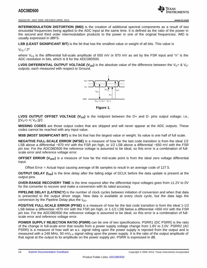
LVDS DIFFERENTIAL OUTPUT VOLTAGE (VOD) is the absolute value of the difference between the VD+ & VD-outputs; each measured with respect to Ground.
Figure 1.
LVDS OUTPUT OFFSET VOLTAGE (VOS) is the midpoint between the D+ and D- pins output voltage; i.e.,[(VD+) +( VD-)]/2.
MISSING CODES are those output codes that are skipped and will never appear at the ADC outputs. Thesecodes cannot be reached with any input value.
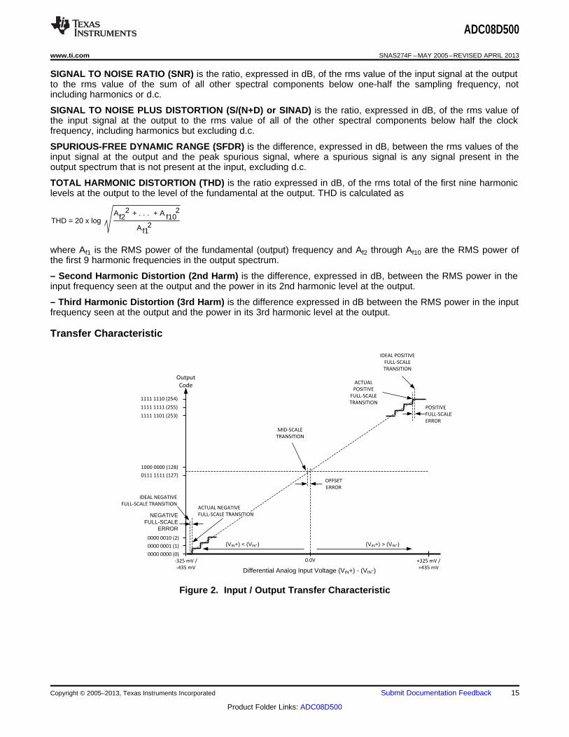
MSB (MOST SIGNIFICANT BIT) is the bit that has the largest value or weight. Its value is one half of full scale.
NEGATIVE FULL-SCALE ERROR (NFSE) is a measure of how far the last code transition is from the ideal 1/2LSB above a differential −870 mV with the FSR pin high, or 1/2 LSB above a differential −650 mV with the FSRpin low. For the ADC08D500 the reference voltage is assumed to be ideal, so this error is a combination of full-scale error and reference voltage error.
OFFSET ERROR (VOFF) is a measure of how far the mid-scale point is from the ideal zero voltage differentialinput.
Offset Error = Actual Input causing average of 8k samples to result in an average code of 127.5.
OUTPUT DELAY (tOD) is the time delay after the falling edge of DCLK before the data update is present at theoutput pins.
OVER-RANGE RECOVERY TIME is the time required after the differential input voltages goes from ±1.2V to 0Vfor the converter to recover and make a conversion with its rated accuracy.
PIPELINE DELAY (LATENCY) is the number of clock cycles between initiation of conversion and when that datais presented to the output driver stage. New data is available at every clock cycle, but the data lags theconversion by the Pipeline Delay plus the tOD.
POSITIVE FULL-SCALE ERROR (PFSE) is a measure of how far the last code transition is from the ideal 1-1/2LSB below a differential +870 mV with the FSR pin high, or 1-1/2 LSB below a differential +650 mV with the FSRpin low. For the ADC08D500 the reference voltage is assumed to be ideal, so this error is a combination of full-scale error and reference voltage error.
POWER SUPPLY REJECTION RATIO (PSRR) can be one of two specifications. PSRR1 (DC PSRR) is the ratioof the change in full-scale error that results from a power supply voltage change from 1.8V to 2.0V. PSRR2 (ACPSRR) is a measure of how well an a.c. signal riding upon the power supply is rejected from the output and ismeasured with a 248 MHz, 50 mVP-P signal riding upon the power supply. It is the ratio of the output amplitude ofthat signal at the output to its amplitude on the power supply pin. PSRR is expressed in dB.
14 Submit Documentation Feedback Copyright © 2005–2013, Texas Instruments Incorporated
Product Folder Links: ADC08D500
ACTUAL
POSITIVE
FULL-SCALE
TRANSITION
-325 mV /
-435 mV
+325 mV /
+435 mV
ACTUAL NEGATIVE
FULL-SCALE TRANSITION
1111 1111 (255)
1111 1110 (254)
1111 1101 (253)
MID-SCALE
TRANSITION
(VIN+) < (VIN-) (VIN+) > (VIN-)
0.0V
Differential Analog Input Voltage (VIN+) - (VIN-)
Output
Code
OFFSET
ERROR
1000 0000 (128)
0111 1111 (127)
0000 0000 (0)
0000 0001 (1)
0000 0010 (2)
IDEAL POSITIVE
FULL-SCALE
TRANSITION
POSITIVE
FULL-SCALE
ERROR
NEGATIVEFULL-SCALE
ERROR
IDEAL NEGATIVE
FULL-SCALE TRANSITION
THD = 20 x log + . . . + AAf2
2 f10
2
Af12
ADC08D500
www.ti.com SNAS274F –MAY 2005–REVISED APRIL 2013
SIGNAL TO NOISE RATIO (SNR) is the ratio, expressed in dB, of the rms value of the input signal at the outputto the rms value of the sum of all other spectral components below one-half the sampling frequency, notincluding harmonics or d.c.
SIGNAL TO NOISE PLUS DISTORTION (S/(N+D) or SINAD) is the ratio, expressed in dB, of the rms value ofthe input signal at the output to the rms value of all of the other spectral components below half the clockfrequency, including harmonics but excluding d.c.
SPURIOUS-FREE DYNAMIC RANGE (SFDR) is the difference, expressed in dB, between the rms values of theinput signal at the output and the peak spurious signal, where a spurious signal is any signal present in theoutput spectrum that is not present at the input, excluding d.c.
TOTAL HARMONIC DISTORTION (THD) is the ratio expressed in dB, of the rms total of the first nine harmoniclevels at the output to the level of the fundamental at the output. THD is calculated as
where Af1 is the RMS power of the fundamental (output) frequency and Af2 through Af10 are the RMS power ofthe first 9 harmonic frequencies in the output spectrum.
– Second Harmonic Distortion (2nd Harm) is the difference, expressed in dB, between the RMS power in theinput frequency seen at the output and the power in its 2nd harmonic level at the output.
– Third Harmonic Distortion (3rd Harm) is the difference expressed in dB between the RMS power in the inputfrequency seen at the output and the power in its 3rd harmonic level at the output.
Transfer Characteristic
Figure 2. Input / Output Transfer Characteristic
Copyright © 2005–2013, Texas Instruments Incorporated Submit Documentation Feedback 15
Product Folder Links: ADC08D500
SCLK
1 12 13 16 17 32
Single Register Access
SCS
SDATA Fixed Header Pattern Register Address
MSB LSB
Register Write Data
tSSU
tSH
tOD
tAD
Sample N
D
Sample N+1
DdSample N-1
VIN
CLK, CLK
DCLK+, DCLK-(0° Phase)
DId, DIDQd, DQ Sample N-14 and Sample N-13Sample N-16 and Sample N-15
Sample N-18 and
Sample N-17
tOSK
DCLK+, DCLK-(90° Phase)
tSU tH
tOD
tAD
Sample N
D
Sample N+1
DdSample N-1
VIN
CLK, CLK
DCLK+, DCLK-(OutEdge = 0)
DId, DIDQd, DQ
Sample N-16 and Sample N-15Sample N-18 and
Sample N-17Sample N-14 and Sample N-13
DCLK+, DCLK-(OutEdge = 1)
tOSK
ADC08D500
SNAS274F –MAY 2005–REVISED APRIL 2013 www.ti.com
Timing Diagrams
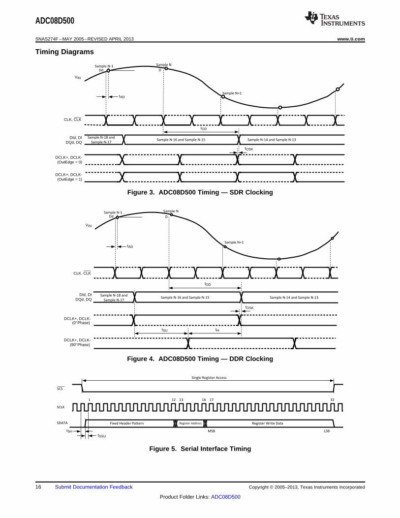
Figure 3. ADC08D500 Timing — SDR Clocking
Figure 4. ADC08D500 Timing — DDR Clocking
Figure 5. Serial Interface Timing
16 Submit Documentation Feedback Copyright © 2005–2013, Texas Instruments Incorporated
Product Folder Links: ADC08D500
tRH
Synchronizing Edge
tRPW
tRStSD
CLK
DCLK_RST
DCLK+
OUTEDGE
tRH
Synchronizing Edge
tRPW
tRStSD
CLK
DCLK_RST
DCLK+
OUTEDGE
CLK
DCLK_RST
tRH
Synchronizing Edge
tRPW
tRS
DCLK+
tAD
ADC08D500
www.ti.com SNAS274F –MAY 2005–REVISED APRIL 2013
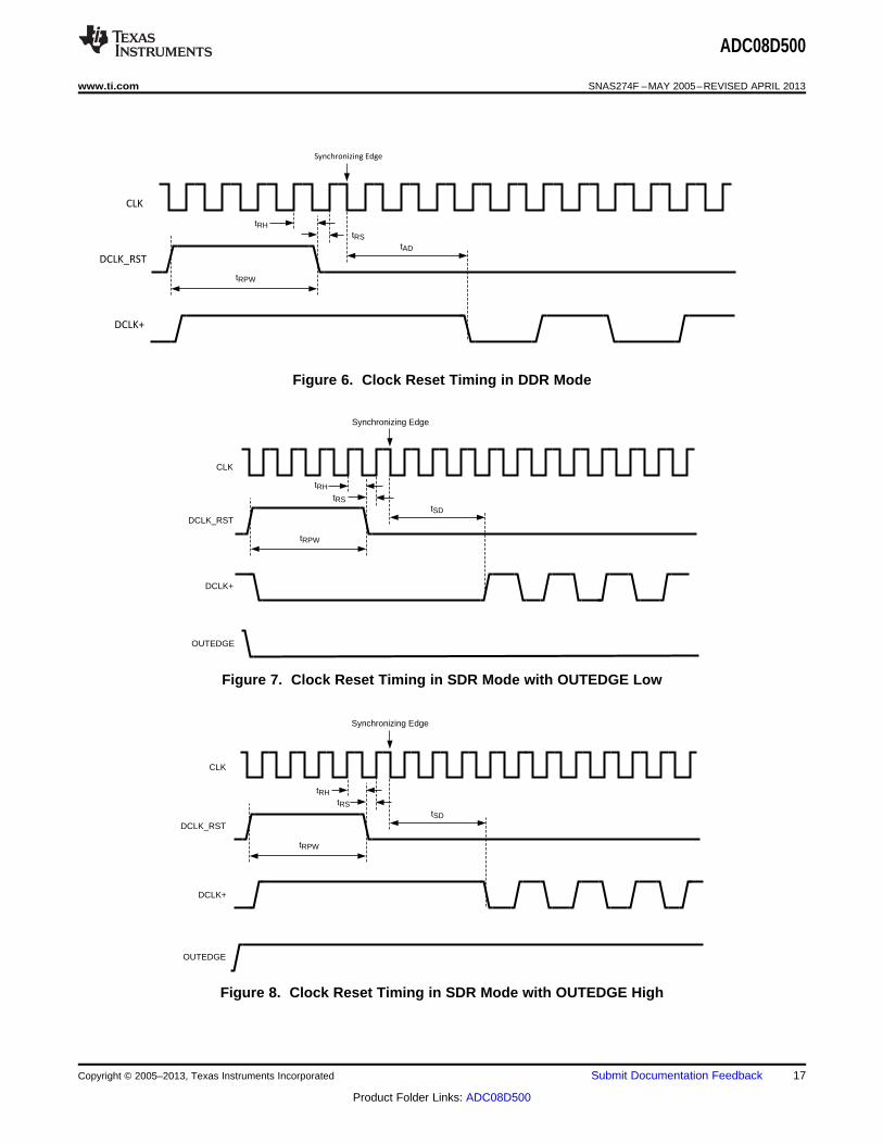
Figure 6. Clock Reset Timing in DDR Mode
Figure 7. Clock Reset Timing in SDR Mode with OUTEDGE Low
Figure 8. Clock Reset Timing in SDR Mode with OUTEDGE High
Copyright © 2005–2013, Texas Instruments Incorporated Submit Documentation Feedback 17
Product Folder Links: ADC08D500

CalRun
POWER
SUPPLY
CAL
tCALtCAL
Calibration Delay
determined by
CalDly Pin (127)
tCalDly
tCAL_L
tCAL_H
ADC08D500
SNAS274F –MAY 2005–REVISED APRIL 2013 www.ti.com
Figure 9. Self Calibration and On-Command Calibration Timing
18 Submit Documentation Feedback Copyright © 2005–2013, Texas Instruments Incorporated
Product Folder Links: ADC08D500
ADC08D500
www.ti.com SNAS274F –MAY 2005–REVISED APRIL 2013
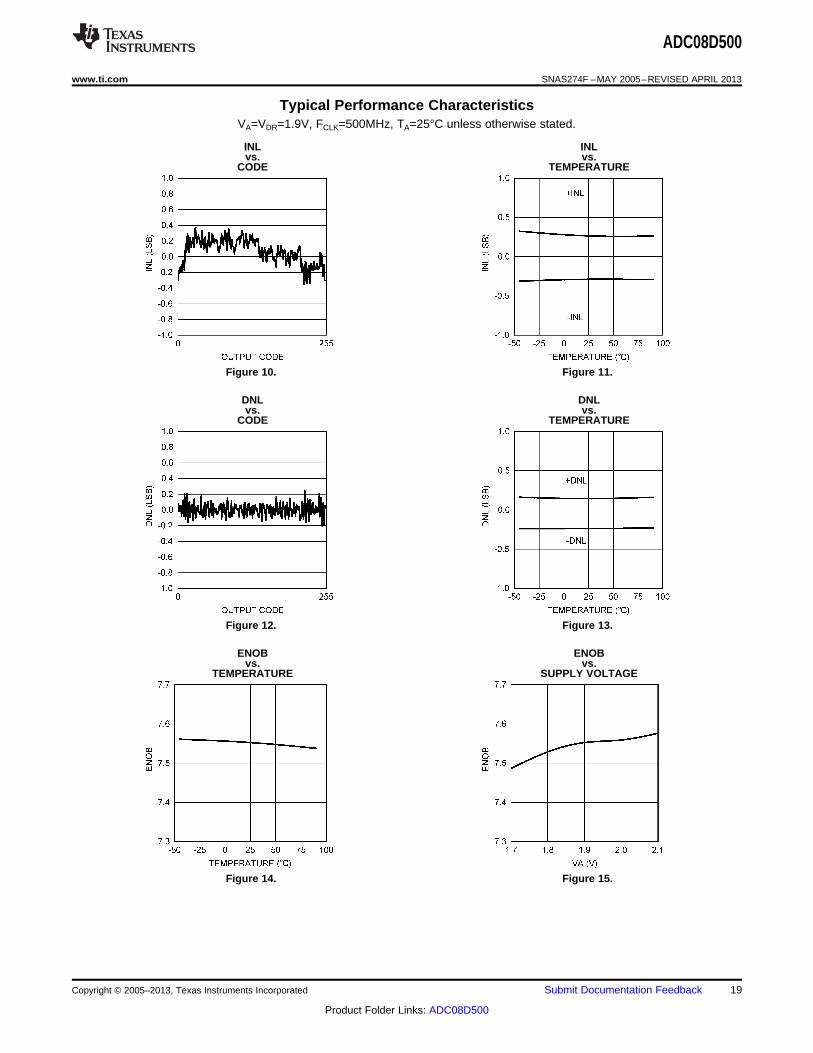
Typical Performance CharacteristicsVA=VDR=1.9V, FCLK=500MHz, TA=25°C unless otherwise stated.
INL INLvs. vs.
CODE TEMPERATURE
Figure 10. Figure 11.
DNL DNLvs. vs.
CODE TEMPERATURE
Figure 12. Figure 13.
ENOB ENOBvs. vs.
TEMPERATURE SUPPLY VOLTAGE
Figure 14. Figure 15.
Copyright © 2005–2013, Texas Instruments Incorporated Submit Documentation Feedback 19
Product Folder Links: ADC08D500
ADC08D500
SNAS274F –MAY 2005–REVISED APRIL 2013 www.ti.com
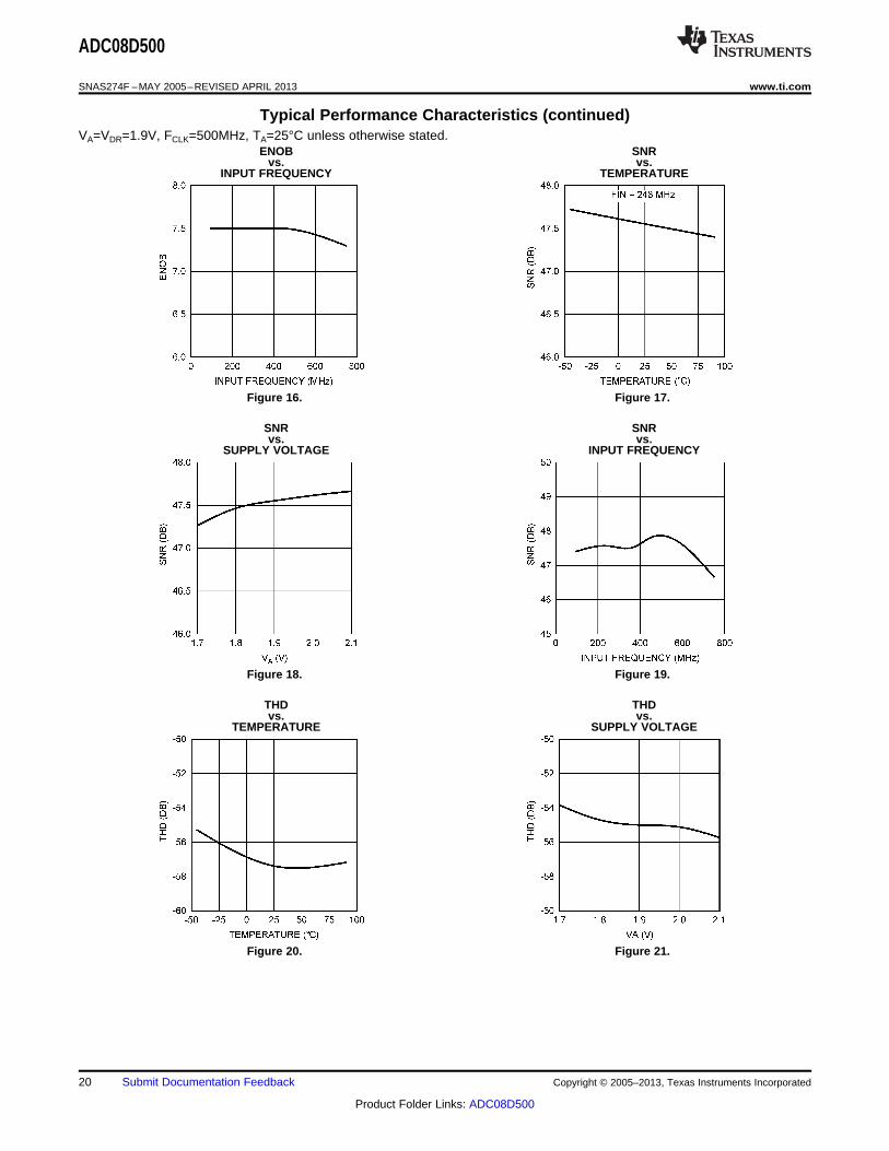
Typical Performance Characteristics (continued)VA=VDR=1.9V, FCLK=500MHz, TA=25°C unless otherwise stated.
ENOB SNRvs. vs.
INPUT FREQUENCY TEMPERATURE
Figure 16. Figure 17.
SNR SNRvs. vs.
SUPPLY VOLTAGE INPUT FREQUENCY
Figure 18. Figure 19.
THD THDvs. vs.
TEMPERATURE SUPPLY VOLTAGE
Figure 20. Figure 21.
20 Submit Documentation Feedback Copyright © 2005–2013, Texas Instruments Incorporated
Product Folder Links: ADC08D500
ADC08D500
www.ti.com SNAS274F –MAY 2005–REVISED APRIL 2013
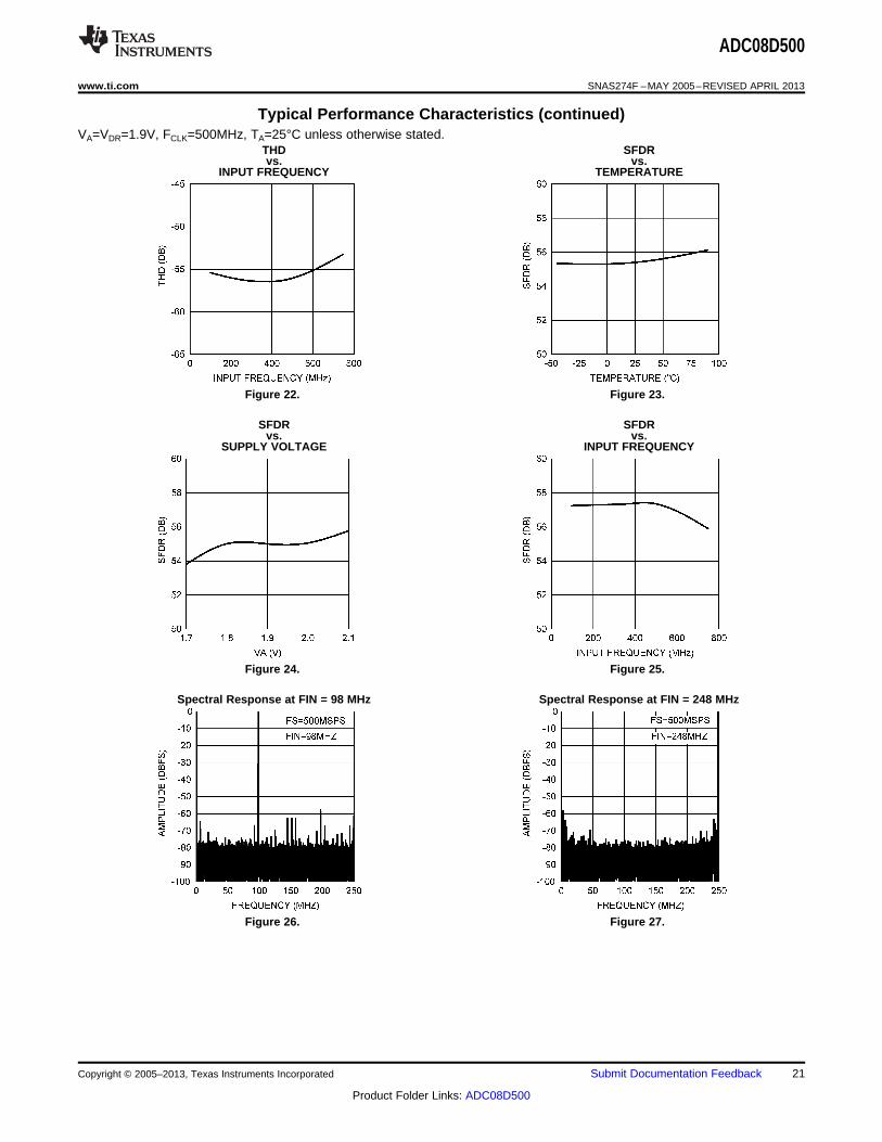
Typical Performance Characteristics (continued)VA=VDR=1.9V, FCLK=500MHz, TA=25°C unless otherwise stated.
THD SFDRvs. vs.
INPUT FREQUENCY TEMPERATURE
Figure 22. Figure 23.
SFDR SFDRvs. vs.
SUPPLY VOLTAGE INPUT FREQUENCY
Figure 24. Figure 25.
Spectral Response at FIN = 98 MHz Spectral Response at FIN = 248 MHz
Figure 26. Figure 27.
Copyright © 2005–2013, Texas Instruments Incorporated Submit Documentation Feedback 21
Product Folder Links: ADC08D500
ADC08D500
SNAS274F –MAY 2005–REVISED APRIL 2013 www.ti.com
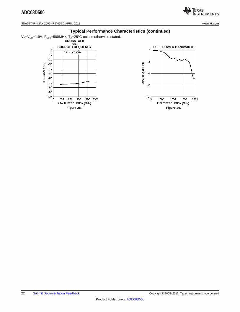
Typical Performance Characteristics (continued)VA=VDR=1.9V, FCLK=500MHz, TA=25°C unless otherwise stated.
CROSSTALKvs.
SOURCE FREQUENCY FULL POWER BANDWIDTH
Figure 28. Figure 29.
22 Submit Documentation Feedback Copyright © 2005–2013, Texas Instruments Incorporated
Product Folder Links: ADC08D500
ADC08D500
www.ti.com SNAS274F –MAY 2005–REVISED APRIL 2013
FUNCTIONAL DESCRIPTION
The ADC08D500 is a versatile A/D Converter with an innovative architecture permitting very high speedoperation. The controls available ease the application of the device to circuit solutions. Optimum performancerequires adherence to the provisions discussed here and in the Applications Information Section.
While it is generally poor practice to allow an active pin to float, pins 4, 14 and 127 of the ADC08D500 aredesigned to be left floating without jeopardy. In all discussions throughout this data sheet, whenever a function iscalled by allowing a pin to float, connecting that pin to a potential of one half the VA supply voltage will have thesame effect as allowing it to float.
OVERVIEW
The ADC08D500 uses a calibrated folding and interpolating architecture that achieves over 7.5 effective bits. Theuse of folding amplifiers greatly reduces the number of comparators and power consumption. Interpolationreduces the number of front-end amplifiers required, minimizing the load on the input signal and further reducingpower requirements. In addition to other things, on-chip calibration reduces the INL bow often seen with foldingarchitectures. The result is an extremely fast, high performance, low power converter.
The analog input signal that is within the converter's input voltage range is digitized to eight bits at speeds of 200MSPS to 500 MSPS, typical. Differential input voltages below negative full-scale will cause the output word toconsist of all zeroes. Differential input voltages above positive full-scale will cause the output word to consist ofall ones. Either of these conditions at either the "I" or "Q" input will cause the OR (Out of Range) output to beactivated. This single OR output indicates when the output code from one or both of the channels is belownegative full scale or above positive full scale.
Each of the two converters has a 1:2 demultiplexer that feeds two LVDS output buses. The data on these busesprovide an output word rate on each bus at half the ADC sampling rate and must be interleaved by the user toprovide output words at the full conversion rate.
The output levels may be selected to be normal or reduced. Using reduced levels saves power but could result inerroneous data capture of some or all of the bits, especially at higher sample rates and in marginally designedsystems.
Self-Calibration
A self-calibration is performed upon power-up and can also be invoked by the user upon command. Calibrationtrims the 100Ω analog input differential termination resistor and minimizes full-scale error, offset error, DNL andINL, resulting in maximizing SNR, THD, SINAD (SNDR) and ENOB. Internal bias currents are also set with thecalibration process. All of this is true whether the calibration is performed upon power up or is performed uponcommand. Running the self calibration is an important part of this chip's functionality and is required in order toobtain adequate performance. In addition to the requirement to be run at power-up, self calibration must be re-run whenever the sense of the FSR pin is changed. For best performance, we recommend that self calibration berun 20 seconds or more after application of power and whenever the operating temperature changessignificantly, according to the particular system design requirements. See On-Command Calibration for moreinformation. Calibration can not be initiated or run while the device is in the power-down mode. See Power Downfor information on the interaction between Power Down and Calibration.
During the calibration process, the input termination resistor is trimmed to a value that is equal to REXT / 33. Thisexternal resistor is located between pin 32 and ground. REXT must be 3300 Ω ±0.1%. With this value, the inputtermination resistor is trimmed to be 100 Ω. Because REXT is also used to set the proper current for the Trackand Hold amplifier, for the preamplifiers and for the comparators, other values of REXT should not be used. Innormal operation, calibration is performed just after application of power and whenever a valid calibrationcommand is given, which is holding the CAL pin low for at least 80 clock cycles, then hold it high for at leastanother 80 clock cycles. The time taken by the calibration procedure is specified in the A.C. CharacteristicsTable. Holding the CAL pin high upon power up will prevent the calibration process from running until the CALpin experiences the above-mentioned 80 clock cycles low followed by 80 clock cycles high.
Copyright © 2005–2013, Texas Instruments Incorporated Submit Documentation Feedback 23
Product Folder Links: ADC08D500
ADC08D500
SNAS274F –MAY 2005–REVISED APRIL 2013 www.ti.com
CalDly (pin 127) is used to select one of two delay times after the application of power to the start of calibration.This calibration delay is 225 clock cycles (about 67.2 ms at 500 MSPS) with CalDly low, or 231 clock cycles (about4.3 seconds at 500 MSPS) with CalDly high. These delay values allow the power supply to come up and stabilizebefore calibration takes place. If the PD pin is high upon power-up, the calibration delay counter will be disableduntil the PD pin is brought low. Therefore, holding the PD pin high during power up will further delay the start ofthe power-up calibration cycle. The best setting of the CalDly pin depends upon the power-on settling time of thepower supply.
The CalRun output is high whenever the calibration procedure is running. This is true whether the calibration isdone at power-up or on-command.
Acquiring the Input
Data is acquired at the falling edge of CLK+ (pin 18) and the digital equivalent of that data is available at thedigital outputs 13 clock cycles later for the DI and DQ output buses and 14 clock cycles later for the DId and DQdoutput buses. There is an additional internal delay called tOD before the data is available at the outputs. See theTiming Diagram. The ADC08D500 will convert as long as the clock signal is present. The fully differentialcomparator design and the innovative design of the sample-and-hold amplifier, together with self calibration,enables a very flat SINAD/ENOB response beyond 500 MHz. The ADC08D500 output data signaling is LVDSand the output format is offset binary.
Control Modes
Much of the user control can be accomplished with several control pins that are provided. Examples includeinitiation of the calibration cycle, power down mode and full scale range setting. However, the ADC08D500 alsoprovides an Extended Control mode whereby a serial interface is used to access register-based control ofseveral advanced features. The Extended Control mode is not intended to be enabled and disabled dynamically.Rather, the user is expected to employ either the normal control mode or the Extended Control mode at all times.When the device is in the Extended Control mode, pin-based control of several features is replaced with register-based control and those pin-based controls are disabled. These pins are OutV (pin 3), OutEdge/DDR (pin 4),FSR (pin 14) and CalDly/DES (pin 127). See NORMAL/EXTENDED CONTROL for details on the ExtendedControl mode.
The Analog Inputs
The ADC08D500 must be driven with a differential input signal. Operation with a single-ended signal is notrecommended. It is important that the inputs either be a.c. coupled to the inputs with the VCMO pin grounded ord.c. coupled with the VCMO pin not grounded and an input common mode voltage equal to the VCMO output.
Two full-scale range settings are provided with pin 14 (FSR). A high on pin 14 causes an input full-scale rangesetting of 870 mVP-P, while grounding pin 14 causes an input full-scale range setting of 650 mVP-P. The full-scalerange setting operates equally on both ADCs.
In the Extended Control mode, the full-scale input range can be set to values between 560 mVP-P and 840 mVP-Pthrough a serial interface. See THE ANALOG INPUT.
Clocking
The ADC08D500 must be driven with an a.c. coupled, differential clock signal. THE CLOCK INPUTS describesthe use of the clock input pins. A differential LVDS output clock is available for use in latching the ADC outputdata into whatever receives that data.
The ADC08D500 offers options for input and output clocking. These options include a choice of Dual EdgeSampling (DES) or interleaved mode where the ADC08D500 performs as a single device converting at twice theinput clock rate and a choice of which DCLK edge the output data transitions on and choice of Single Data Rate(SDR) or Double Data Rate (DDR) outputs.
The ADC08D500 also has the option to use a duty cycle corrected clock receiver as part of the input clockcircuit. This feature is enabled by default and provides improved ADC clocking, especially in the Dual-EdgeSampling mode (DES). This circuitry allows the ADC to be clocked with a signal source having a duty cycle ratioof 80 / 20 % (worst case) for both the normal and the Dual Edge Sampling modes.
24 Submit Documentation Feedback Copyright © 2005–2013, Texas Instruments Incorporated
Product Folder Links: ADC08D500
ADC08D500
www.ti.com SNAS274F –MAY 2005–REVISED APRIL 2013
Dual-Edge Sampling
The DES mode allows one of the ADC08D500's inputs (I or Q Channel) to be sampled by both ADCs. One ADCsamples the input on the positive edge of the input clock and the other ADC samples the same input on the otheredge of the input clock. A single input is thus sampled twice per clock cycle, resulting in an overall sample rate oftwice the input clock frequency, or 1 GSPS with a 500 MHz clock.
In this mode the outputs are interleaved such that the data is effectively demultiplexed 1:4. Since the sample rateis doubled, each of the 4 output buses have a 250 MSPS output rate with a 500 MHz input clock. All data isavailable in parallel. The four bytes of parallel data that is output with each clock is in the following samplingorder, from the earliest to the latest: DQd, DId, DQ, DI. Table 1 indicates what the outputs represent for thevarious sampling possibilities.
In the non-extended mode of operation only the "I" input can be sampled in the DES mode. In the extendedmode of operation the user can select which input is sampled.
The ADC08D500 also includes an automatic clock phase background calibration feature which can be used inDES mode to automatically and continuously adjust the clock phase of the I and Q channel. This featureremoves the need to adjust the clock phase setting manually and provides optimal Dual-Edge Sampling ENOBperformance.
NOTEThe background calibration feature in DES mode does not replace the requirement for On-Command Calibration which should be run before entering DES mode, or if a large swingin ambient temperature is experienced by the device.
Table 1. Input Channel Samples Produced at Data Outputs
Data Outputs Dual-Edge Sampling Mode(Always sourced with Normal Sampling Mode
I-Channel Selected Q-Channel Selected (1)respect to fall of DCLK)
"I" Input Sampled with Fall of "I" Input Sampled with Fall of "Q" Input Sampled with Fall ofDI CLK 13 cycles earlier. CLK 13 cycles earlier. CLK 13 cycles earlier.
"I" Input Sampled with Fall of "I" Input Sampled with Fall of "Q" Input Sampled with Fall ofDId CLK 14 cycles earlier. CLK 14 cycles earlier. CLK 14 cycles earlier.
"Q" Input Sampled with Fall of "I" Input Sampled with Rise of "Q" Input Sampled with Rise ofDQ CLK 13 cycles earlier. CLK 13.5 cycles earlier. CLK 13.5 cycles earlier.
"Q" Input Sampled with Fall of "I" Input Sampled with Rise of "Q" Input Sampled with Rise ofDQd CLK 14 cycles after being CLK 14.5 cycles earlier. CLK 14.5 cycles earlier.sampled.
(1) In DES + normal mode, only the I Channel is sampled. In DES + extended control mode, I or Q channel can be sampled.
OutEdge Setting
To help ease data capture in the SDR mode, the output data may be caused to transition on either the positive orthe negative edge of the output data clock (DCLK). This is chosen with the OutEdge input (pin 4). A high on theOutEdge input causes the output data to transition on the rising edge of DCLK, while grounding this input causesthe output to transition on the falling edge of DCLK. See Output Edge Synchronization.
Double Data Rate
A choice of single data rate (SDR) or double data rate (DDR) output is offered. With single data rate the clockfrequency is the same as the data rate of the two output buses. With double data rate the clock frequency is halfthe data rate and data is sent to the outputs on both DCLK edges. DDR clocking is enabled in non-ExtendedControl mode by allowing pin 4 to float.
Copyright © 2005–2013, Texas Instruments Incorporated Submit Documentation Feedback 25
Product Folder Links: ADC08D500

ADC08D500
SNAS274F –MAY 2005–REVISED APRIL 2013 www.ti.com
The LVDS Outputs
The data outputs, the Out Of Range (OR) and DCLK, are LVDS. Output current sources provide 3 mA of outputcurrent to a differential 100 Ohm load when the OutV input (pin 14) is high or 2.2 mA when the OutV input is low.For short LVDS lines and low noise systems, satisfactory performance may be realized with the OutV input low,which results in lower power consumption. If the LVDS lines are long and/or the system in which theADC08D500 is used is noisy, it may be necessary to tie the OutV pin high. The LVDS data output have a typicalcommon mode voltage of 800mV when the VBG pin is unconnected and floating. This common mode voltage canbe increased to 1.2V by tying the VBG pin to VA if a higher common mode is required.
NOTETying the VBG pin to VA will also increase the differential LVDS output voltage by up to40mV.
Power Down
The ADC08D500 is in the active state when the Power Down pin (PD) is low. When the PD pin is high, thedevice is in the power down mode, where the output pins hold the last conversion before the PD pin went highand the device power consumption is reduced to a minimal level. A high on the PDQ pin will power down the "Q"channel and leave the "I" channel active. There is no provision to power down the "I" channel independently ofthe "Q" channel. Upon return to normal operation, the pipeline will contain meaningless information.
If the PD input is brought high while a calibration is running, the device will not go into power down until thecalibration sequence is complete. However, if power is applied and PD is already high, the device will not beginthe calibration sequence until the PD input goes low. If a manual calibration is requested while the device ispowered down, the calibration will not begin at all. That is, the manual calibration input is completely ignored inthe power down state. Calibration will function with the "Q" channel powered down, but that channel will not becalibrated if PDQ is high. If the "Q" channel is subsequently to be used, it is necessary to perform a calibrationafter PDQ is brought low.
NORMAL/EXTENDED CONTROL
The ADC08D500 may be operated in one of two modes. In the simpler "normal" control mode, the user affectsavailable configuration and control of the device through several control pins. The "extended control mode"provides additional configuration and control options through a serial interface and a set of 8 registers. The twocontrol modes are selected with pin 14 (FSR/ECE: Extended Control Enable). The choice of control modes isrequired to be a fixed selection and is not intended to be switched dynamically while the device is operational.
Table 2 shows how several of the device features are affected by the control mode chosen.
Table 2. Features and Modes
Feature Normal Control Mode Extended Control Mode
Selected with DE bit in the ConfigurationSDR or DDR Clocking Selected with pin 4 Register (1h).
Selected with DCP bit in the ConfigurationDDR Clock Phase Not Selectable (0° Phase Only) Register (1h). See REGISTER DESCRIPTION
SDR Data transitions with rising or falling Selected with the OE bit in the ConfigurationSelected with pin 4DCLK edge Register (1h).
Selected with the OV bit in the ConfigurationLVDS output level Selected with pin 3 Register (1h).
Power-On Calibration Delay Delay Selected with pin 127 Short delay only.
Up to 512 step adjustments over a nominalOptions (650 mVP-P or 870 mVP-P) selected range of 560 mV to 840 mV. Separate rangeFull-Scale Range with pin 14. Selected range applies to both selected for I- and Q-Channels. Selected usingchannels. registers 3h and Bh.
Separate ±45 mV adjustments in 512 steps forInput Offset Adjust Not possible each channel using registers 2h and Ah.
Dual Edge Sampling Selection Enabled with pin 127 Enabled through DES Enable Register (1h).
Dual Edge Sampling Input Channel Either I- or Q-Channel input may be sampledOnly I-Channel Input can be usedSelection by both ADCs
26 Submit Documentation Feedback Copyright © 2005–2013, Texas Instruments Incorporated
Product Folder Links: ADC08D500

ADC08D500
www.ti.com SNAS274F –MAY 2005–REVISED APRIL 2013
Table 2. Features and Modes (continued)
Automatic Clock Phase control can be selectedby setting bit 14 in the DES Enable register
DES Sampling Clock Adjustment The Clock Phase is adjusted automatically (Dh). The clock phase can also be adjustedmanually through the Coarse & Fine registersEh and Fh.
The default state of the Extended Control Mode is set upon power-on reset (internally performed by the device)and is shown in Table 3.
Table 3. Extended Control Mode Operation(Pin 14 Floating)
Feature Extended Control Mode Default State
SDR or DDR Clocking DDR Clocking
DDR Clock Phase Data changes with DCLK edge (0° phase)
Normal amplitudeLVDS Output Amplitude (710 mVP-P)
Calibration Delay Short Delay
Full-Scale Range 700 mV nominal for both channels
Input Offset Adjust No adjustment for either channel
Dual Edge Sampling (DES) Not enabled
THE SERIAL INTERFACE
NOTEDuring the initial write using the serial interface, all 8 user registers must be written withdesired or default values. In addition, the first write to the DES Enable register (Dh) mustload the default value (0x3FFFh). Once all registers have been written once, other desiredsettings, including enabling DES can be loaded.
The 3-pin serial interface is enabled only when the device is in the Extended Controlmode. The pins of this interface are Serial Clock (SCLK), Serial Data (SDATA) and SerialInterface Chip Select (SCS) Eight write only registers are accessible through this serialinterface.
SCS: This signal should be asserted low while accessing a register through the serial interface. Setup and holdtimes with respect to the SCLK must be observed.
SCLK: Serial data input is accepted with the rising edge of this signal. There is no minimum frequencyrequirement for SCLK.
SDATA: Each register access requires a specific 32-bit pattern at this input. This pattern consists of a header,register address and register value. The data is shifted in MSB first. Setup and hold times with respect to theSCLK must be observed. See the Timing Diagram.
Each Register access consists of 32 bits, as shown in Figure 5 of the Timing Diagrams. The fixed header patternis 0000 0000 0001 (eleven zeros followed by a 1). The loading sequence is such that a 0b is loaded first. These12 bits form the header. The next 4 bits are the address of the register that is to be written to and the last 16 bitsare the data written to the addressed register. The addresses of the various registers are indicated in Table 4.
Refer to the REGISTER DESCRIPTION for information on the data to be written to the registers.
Subsequent register accesses may be performed immediately, starting with the 33rd SCLK. This means that theSCS input does not have to be de-asserted and asserted again between register addresses. It is possible,although not recommended, to keep the SCS input permanently enabled (at a logic low) when using extendedcontrol.
Copyright © 2005–2013, Texas Instruments Incorporated Submit Documentation Feedback 27
Product Folder Links: ADC08D500
ADC08D500
SNAS274F –MAY 2005–REVISED APRIL 2013 www.ti.com
NOTEThe Serial Interface should not be used when calibrating the ADC. Doing so will impair theperformance of the device until it is re-calibrated correctly. Programming the serialregisters will also reduce dynamic performance of the ADC for the duration of the registeraccess time.
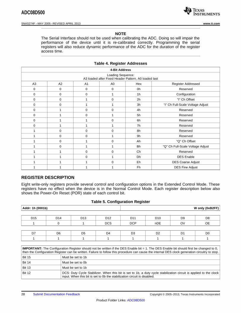
Table 4. Register Addresses
4-Bit Address
Loading Sequence:A3 loaded after Fixed Header Pattern, A0 loaded last
A3 A2 A1 A0 Hex Register Addressed
0 0 0 0 0h Reserved
0 0 0 1 1h Configuration
0 0 1 0 2h "I" Ch Offset
0 0 1 1 3h "I" Ch Full-Scale Voltage Adjust
0 1 0 0 4h Reserved
0 1 0 1 5h Reserved
0 1 1 0 6h Reserved
0 1 1 1 7h Reserved
1 0 0 0 8h Reserved
1 0 0 1 9h Reserved
1 0 1 0 Ah "Q" Ch Offset
1 0 1 1 Bh "Q" Ch Full-Scale Voltage Adjust
1 1 0 0 Ch Reserved
1 1 0 1 Dh DES Enable
1 1 1 0 Eh DES Coarse Adjust
1 1 1 1 Fh DES Fine Adjust
REGISTER DESCRIPTION
Eight write-only registers provide several control and configuration options in the Extended Control Mode. Theseregisters have no effect when the device is in the Normal Control Mode. Each register description below alsoshows the Power-On Reset (POR) state of each control bit.
Table 5. Configuration Register
Addr: 1h (0001b) W only (0xB2FF)
D15 D14 D13 D12 D11 D10 D9 D8
1 0 1 DCS DCP nDE OV OE
D7 D6 D5 D4 D3 D2 D1 D0
1 1 1 1 1 1 1 1
IMPORTANT: The Configuration Register should not be written if the DES Enable bit = 1. The DES Enable bit should first be changed to 0,then the Configuration Register can be written. Failure to follow this procedure can cause the internal DES clock generation circuitry to stop.
Bit 15 Must be set to 1b
Bit 14 Must be set to 0b
Bit 13 Must be set to 1b
Bit 12 DCS: Duty Cycle Stabilizer. When this bit is set to 1b, a duty cycle stabilization circuit is applied to the clockinput. When this bit is set to 0b the stabilization circuit is disabled.
28 Submit Documentation Feedback Copyright © 2005–2013, Texas Instruments Incorporated
Product Folder Links: ADC08D500
ADC08D500
www.ti.com SNAS274F –MAY 2005–REVISED APRIL 2013
Bit 11 DCP: DDR Clock Phase. This bit only has an effect in the DDR mode. When this bit is set to 0b, the DCLKedges are time-aligned with the data bus edges ("0° Phase"). When this bit is set to 1b, the DCLK edges areplaced in the middle of the data bit-cells ("90° Phase"), using the one-half speed DCLK shown in Figure 4 asthe phase reference.
POR State: 0b
Bit 10 nDE: DDR Enable. When this bit is set to 0b, data bus clocking follows the DDR (Dual Data Rate) modewhereby a data word is output with each rising and falling edge of DCLK. When this bit is set to a 1b, data busclocking follows the SDR (single data rate) mode whereby each data word is output with either the rising orfalling edge of DCLK, as determined by the OutEdge bit.
POR State: 0b
Bit 9 OV: Output Voltage. This bit determines the LVDS outputs' voltage amplitude and has the same function as theOutV pin that is used in the normal control mode. When this bit is set to 1b, the standard output amplitude of710 mVP-P is used. When this bit is set to 0b, the reduced output amplitude of 510 mVP-P is used.
POR State: 1b
Bit 8 OE: Output Edge. This bit selects the DCLK edge with which the data words transition in the SDR mode andhas the same effect as the OutEdge pin in the normal control mode. When this bit is 1b, the data outputschange with the rising edge of DCLK+. When this bit is 0b, the data output change with the falling edge ofDCLK+.
POR State: 0b
Bits 7:0 Must be set to 1b.
Table 6. I-Channel Offset
Addr: 2h (0010b) W only (0x007F)
D15 D14 D13 D12 D11 D10 D9 D8
(MSB) Offset Value (LSB)
D7 D6 D5 D4 D3 D2 D1 D0
Sign 1 1 1 1 1 1 1
Bits 15:8 Offset Value. The input offset of the I-Channel ADC is adjusted linearly and monotonically by the value in thisfield. 00h provides a nominal zero offset, while FFh provides a nominal 45 mV of offset. Thus, each code stepprovides 0.176 mV of offset.
POR State: 0000 0000b
Bit 7 Sign bit. 0b gives positive offset, 1b gives negative offset.
POR State: 0b
Bit 6:0 Must be set to 1b
Table 7. I-Channel Full-Scale Voltage Adjust
Addr: 3h (0011b) W only (0x807F)
D15 D14 D13 D12 D11 D10 D9 D8
(MSB) Adjust Value
D7 D6 D5 D4 D3 D2 D1 D0
(LSB) 1 1 1 1 1 1 1
Copyright © 2005–2013, Texas Instruments Incorporated Submit Documentation Feedback 29
Product Folder Links: ADC08D500
ADC08D500
SNAS274F –MAY 2005–REVISED APRIL 2013 www.ti.com
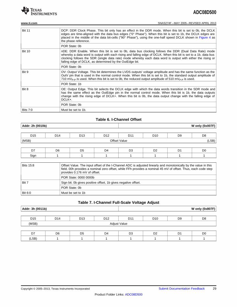
Bit 15:7 Full Scale Voltage Adjust Value. The input full-scale voltage of the I-Channel ADC is adjusted linearly andmonotonically from the nominal 700 mVP-P differential by the value in this field.
0000 0000 0 560mVP-P
1000 0000 0 700mVP-P
1111 1111 1 840mVP-P
For best performance, it is recommended that the value in this field be limited to the range of 0110 0000 0b to1110 0000 0b. i.e., limit the amount of adjustment to ±15%. The remaining ±5% headroom allows for the ADC'sown full scale variation .A gain adjustment does not require ADC re-calibration.
POR State: 1000 0000 0b (no adjustment)
Bits 6:0 Must be set to 1b
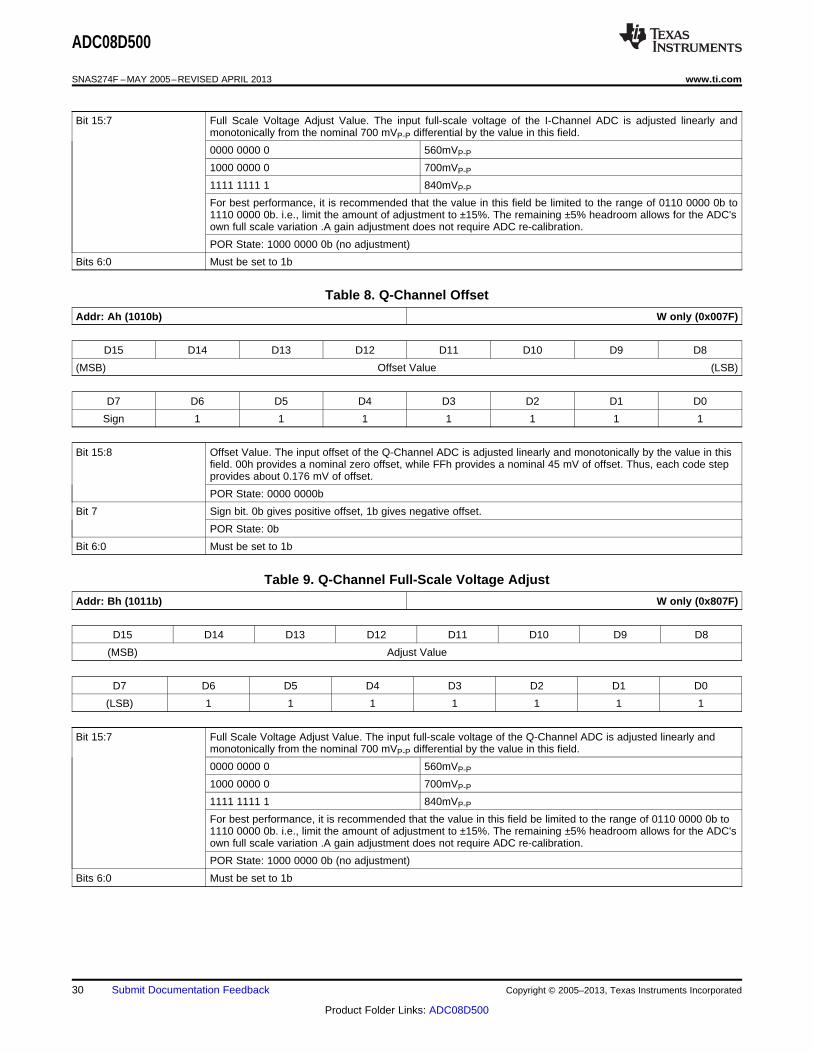
Table 8. Q-Channel Offset
Addr: Ah (1010b) W only (0x007F)
D15 D14 D13 D12 D11 D10 D9 D8
(MSB) Offset Value (LSB)
D7 D6 D5 D4 D3 D2 D1 D0
Sign 1 1 1 1 1 1 1
Bit 15:8 Offset Value. The input offset of the Q-Channel ADC is adjusted linearly and monotonically by the value in thisfield. 00h provides a nominal zero offset, while FFh provides a nominal 45 mV of offset. Thus, each code stepprovides about 0.176 mV of offset.
POR State: 0000 0000b
Bit 7 Sign bit. 0b gives positive offset, 1b gives negative offset.
POR State: 0b
Bit 6:0 Must be set to 1b
Table 9. Q-Channel Full-Scale Voltage Adjust
Addr: Bh (1011b) W only (0x807F)
D15 D14 D13 D12 D11 D10 D9 D8
(MSB) Adjust Value
D7 D6 D5 D4 D3 D2 D1 D0
(LSB) 1 1 1 1 1 1 1
Bit 15:7 Full Scale Voltage Adjust Value. The input full-scale voltage of the Q-Channel ADC is adjusted linearly andmonotonically from the nominal 700 mVP-P differential by the value in this field.
0000 0000 0 560mVP-P
1000 0000 0 700mVP-P
1111 1111 1 840mVP-P
For best performance, it is recommended that the value in this field be limited to the range of 0110 0000 0b to1110 0000 0b. i.e., limit the amount of adjustment to ±15%. The remaining ±5% headroom allows for the ADC'sown full scale variation .A gain adjustment does not require ADC re-calibration.
POR State: 1000 0000 0b (no adjustment)
Bits 6:0 Must be set to 1b
30 Submit Documentation Feedback Copyright © 2005–2013, Texas Instruments Incorporated
Product Folder Links: ADC08D500
ADC08D500
www.ti.com SNAS274F –MAY 2005–REVISED APRIL 2013
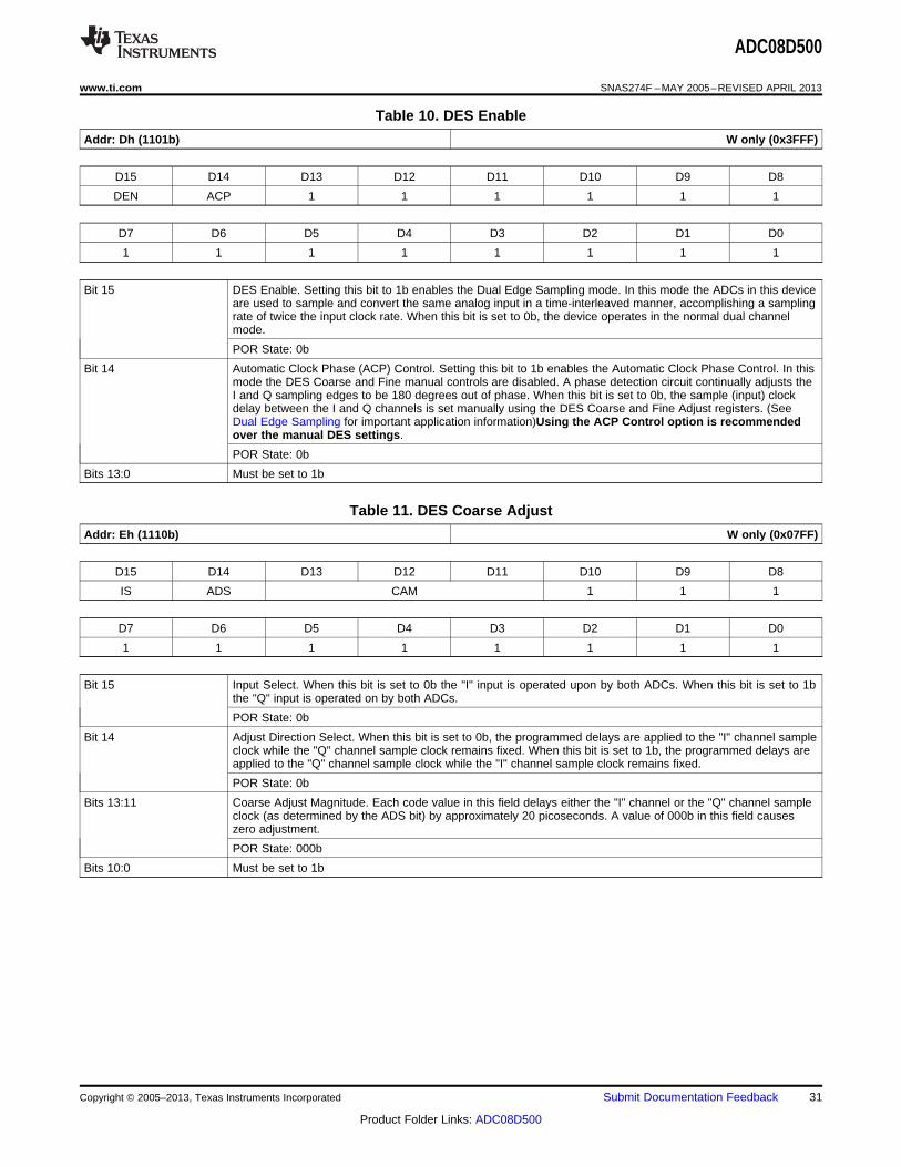
Table 10. DES Enable
Addr: Dh (1101b) W only (0x3FFF)
D15 D14 D13 D12 D11 D10 D9 D8
DEN ACP 1 1 1 1 1 1
D7 D6 D5 D4 D3 D2 D1 D0
1 1 1 1 1 1 1 1
Bit 15 DES Enable. Setting this bit to 1b enables the Dual Edge Sampling mode. In this mode the ADCs in this deviceare used to sample and convert the same analog input in a time-interleaved manner, accomplishing a samplingrate of twice the input clock rate. When this bit is set to 0b, the device operates in the normal dual channelmode.
POR State: 0b
Bit 14 Automatic Clock Phase (ACP) Control. Setting this bit to 1b enables the Automatic Clock Phase Control. In thismode the DES Coarse and Fine manual controls are disabled. A phase detection circuit continually adjusts theI and Q sampling edges to be 180 degrees out of phase. When this bit is set to 0b, the sample (input) clockdelay between the I and Q channels is set manually using the DES Coarse and Fine Adjust registers. (SeeDual Edge Sampling for important application information)Using the ACP Control option is recommendedover the manual DES settings.
POR State: 0b
Bits 13:0 Must be set to 1b
Table 11. DES Coarse Adjust
Addr: Eh (1110b) W only (0x07FF)
D15 D14 D13 D12 D11 D10 D9 D8
IS ADS CAM 1 1 1
D7 D6 D5 D4 D3 D2 D1 D0
1 1 1 1 1 1 1 1
Bit 15 Input Select. When this bit is set to 0b the "I" input is operated upon by both ADCs. When this bit is set to 1bthe "Q" input is operated on by both ADCs.
POR State: 0b
Bit 14 Adjust Direction Select. When this bit is set to 0b, the programmed delays are applied to the "I" channel sampleclock while the "Q" channel sample clock remains fixed. When this bit is set to 1b, the programmed delays areapplied to the "Q" channel sample clock while the "I" channel sample clock remains fixed.
POR State: 0b
Bits 13:11 Coarse Adjust Magnitude. Each code value in this field delays either the "I" channel or the "Q" channel sampleclock (as determined by the ADS bit) by approximately 20 picoseconds. A value of 000b in this field causeszero adjustment.
POR State: 000b
Bits 10:0 Must be set to 1b
Copyright © 2005–2013, Texas Instruments Incorporated Submit Documentation Feedback 31
Product Folder Links: ADC08D500
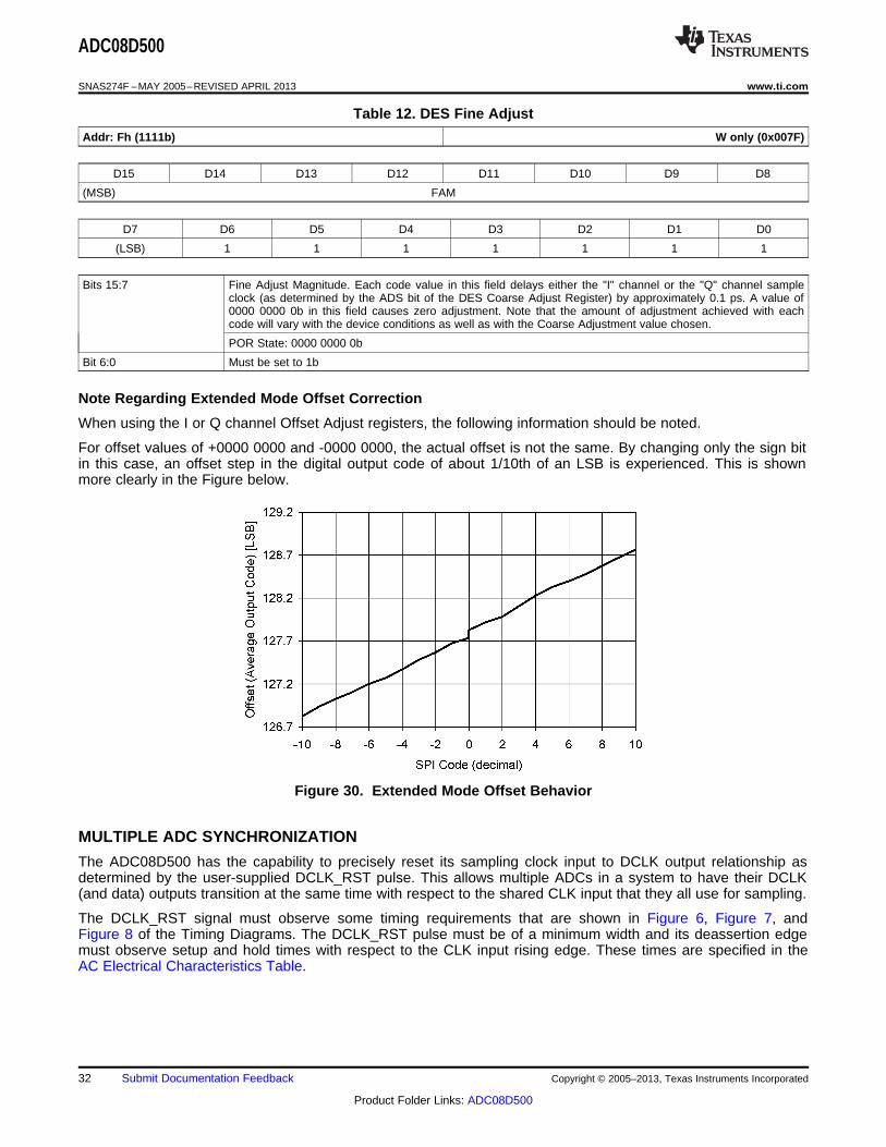
ADC08D500
SNAS274F –MAY 2005–REVISED APRIL 2013 www.ti.com
Table 12. DES Fine Adjust
Addr: Fh (1111b) W only (0x007F)
D15 D14 D13 D12 D11 D10 D9 D8
(MSB) FAM
D7 D6 D5 D4 D3 D2 D1 D0
(LSB) 1 1 1 1 1 1 1
Bits 15:7 Fine Adjust Magnitude. Each code value in this field delays either the "I" channel or the "Q" channel sampleclock (as determined by the ADS bit of the DES Coarse Adjust Register) by approximately 0.1 ps. A value of0000 0000 0b in this field causes zero adjustment. Note that the amount of adjustment achieved with eachcode will vary with the device conditions as well as with the Coarse Adjustment value chosen.
POR State: 0000 0000 0b
Bit 6:0 Must be set to 1b
Note Regarding Extended Mode Offset Correction
When using the I or Q channel Offset Adjust registers, the following information should be noted.
For offset values of +0000 0000 and -0000 0000, the actual offset is not the same. By changing only the sign bitin this case, an offset step in the digital output code of about 1/10th of an LSB is experienced. This is shownmore clearly in the Figure below.
Figure 30. Extended Mode Offset Behavior
MULTIPLE ADC SYNCHRONIZATION
The ADC08D500 has the capability to precisely reset its sampling clock input to DCLK output relationship asdetermined by the user-supplied DCLK_RST pulse. This allows multiple ADCs in a system to have their DCLK(and data) outputs transition at the same time with respect to the shared CLK input that they all use for sampling.
The DCLK_RST signal must observe some timing requirements that are shown in Figure 6, Figure 7, andFigure 8 of the Timing Diagrams. The DCLK_RST pulse must be of a minimum width and its deassertion edgemust observe setup and hold times with respect to the CLK input rising edge. These times are specified in theAC Electrical Characteristics Table.
32 Submit Documentation Feedback Copyright © 2005–2013, Texas Instruments Incorporated
Product Folder Links: ADC08D500

ADC08D500
www.ti.com SNAS274F –MAY 2005–REVISED APRIL 2013
The DCLK_RST signal can be asserted asynchronous to the input clock If DCLK_RST is asserted, the DCLKoutput is held in a designated state. The state in which DCLK is held during the reset period is determined by themode of operation (SDR/DDR) and the setting of the Output Edge configuration pin or bit. (Refer to Figure 6,Figure 8, and Figure 8 for the DCLK reset conditions). Therefore depending upon when the DCLK_RST signal isasserted, there may be a narrow pulse on the DCLK line during this reset event. When the DCLK_RST signal isde-asserted in synchronization with the CLK rising edge, the next CLK falling edge synchronizes the DCLKoutput with those of other ADC08D500s in the system. The DCLK output is enabled again after a constant delaywhich is equal to the CLK input to DCLK output delay (tAD). The device always exhibits this delay characteristic innormal operation.
The DCLK-RST pin should NOT be brought high while the calibration process is running (while CalRun is high).Doing so could cause a digital glitch in the digital circuitry, resulting in corruption and invalidation of thecalibration.
Applications Information
THE REFERENCE VOLTAGE
The voltage reference for the ADC08D500 is derived from a 1.254V bandgap reference which is made availableat pin 31, VBG for user convenience and has an output current capability of ±100 μA and should be buffered ifmore current than this is required.
The internal bandgap-derived reference voltage has a nominal value of 650 mV or 870 mV, as determined by theFSR pin and described in The Analog Inputs.
There is no provision for the use of an external reference voltage, but the full-scale input voltage can be adjustedthrough a Configuration Register in the Extended Control mode, as explained in NORMAL/EXTENDEDCONTROL.
Differential input signals up to the chosen full-scale level will be digitized to 8 bits. Signal excursions beyond thefull-scale range will be clipped at the output. These large signal excursions will also activate the OR output forthe time that the signal is out of range. See Out Of Range (OR) Indication.
One extra feature of the VBG pin is that it can be used to raise the common mode voltage level of the LVDSoutputs. The output offset voltage (VOS) is typically 800mV when the VBG pin is used as an output or leftunconnected. To raise the LVDS offset voltage to a typical value of 1200mV the VBG pin can be connecteddirectly to the supply rails.
THE ANALOG INPUT
The analog input is a differential one to which the signal source may be a.c. coupled or d.c. coupled. The full-scale input range is selected with the FSR pin to be 650 mVP-P or 870 mVP-P, or can be adjusted to valuesbetween 560 mVP-P and 840 mVP-P in the Extended Control mode through the Serial Interface. For bestperformance, it is recommended that the full-scale range be kept between 595 mVP-P and 805 mVP-P in theExtended Control mode.
Table 13 gives the input to output relationship with the FSR pin high and the normal (non-extended) mode isused. With the FSR pin grounded, the millivolt values in Table 13 are reduced to 75% of the values indicated. Inthe Enhanced Control Mode, these values will be determined by the full scale range and offset settings in theControl Registers.
Table 13. Differential Input To Output Relationship(Non-Extended Control Mode, FSR High)
VIN+ VIN− Output Code
VCM − 217.5mV VCM + 217.5mV 0000 0000
VCM − 109mV VCM + 109mV 0100 0000
0111 1111 /VCM VCM 1000 0000
VCM + 109 mV VCM − 109mV 1100 0000
VCM + 217.5mV VCM − 217.5mV 1111 1111
Copyright © 2005–2013, Texas Instruments Incorporated Submit Documentation Feedback 33
Product Folder Links: ADC08D500

AD
C08
D50
0
RA
DJ-
VIN-
VIN+
VCMO
50:
SignalInput
LMV321
+
-
LMH6555RA
DJ+
3.3V
RT2
50:
RT1
50:
RF1
RF2
RG1
RG2
VCM_REF
50:
100:
+
-
50:
VIN+
VIN-
VCMO
ADC08D500
Ccouple
Ccouple
ADC08D500
SNAS274F –MAY 2005–REVISED APRIL 2013 www.ti.com
The buffered analog inputs simplify the task of driving these inputs and the RC pole that is generally used atsampling ADC inputs is not required. If it is desired to use an amplifier circuit before the ADC, use care inchoosing an amplifier with adequate noise and distortion performance and adequate gain at the frequencies usedfor the application.
Note that a precise d.c. common mode voltage must be present at the ADC inputs. This common mode voltage,VCMO, is provided on-chip when a.c. input coupling is used and the input signal is a.c. coupled to the ADC.
When the inputs are a.c. coupled, the VCMO output must be grounded, as shown in Figure 31. This causes theon-chip VCMO voltage to be connected to the inputs through on-chip 50k-Ohm resistors.
NOTEAn Analog input channel that is not used (e.g. in DES Mode) should be left floating whenthe inputs are a.c. coupled. Do not connect an unused analog input to ground.
Figure 31. Differential Input Drive
When the d.c. coupled mode is used, a common mode voltage must be provided at the differential inputs. Thiscommon mode voltage should track the VCMO output pin. Note that the VCMO output potential will change withtemperature. The common mode output of the driving device should track this change.
NOTEAn analog input channel that is not used (e.g. in DES Mode) should be tied to the VCMOvoltage when the inputs are d.c. coupled. Do not connect unused analog inputs to ground.
Full-scale distortion performance falls off rapidly as the input common mode voltage deviates from VCMO.This is a direct result of using a very low supply voltage to minimize power. Keep the input commonvoltage within 50 mV of VCMO.
Performance is as good in the d.c. coupled mode as it is in the a.c. coupled mode, provided the inputcommon mode voltage at both analog inputs remain within 50 mV of VCMO.
If d.c. coupling is used, it is best to servo the input common mode voltage with VCMO to maintain optimumperformance. An example of this type of circuit is shown in Figure 32.
Figure 32. Example of Servoing the Analog Input with VCMO
34 Submit Documentation Feedback Copyright © 2005–2013, Texas Instruments Incorporated
Product Folder Links: ADC08D500
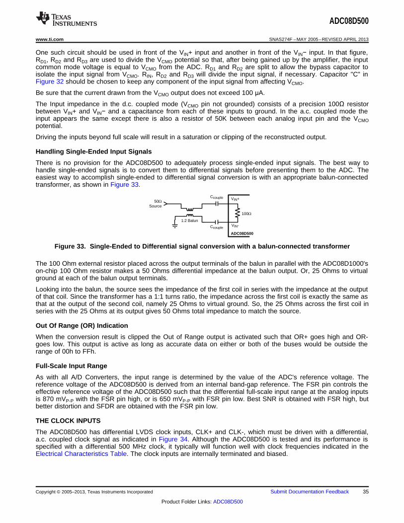
VIN+50:
Source
VIN-1:2 Balun
Ccouple
Ccouple
100:
ADC08D500
ADC08D500
www.ti.com SNAS274F –MAY 2005–REVISED APRIL 2013
One such circuit should be used in front of the VIN+ input and another in front of the VIN− input. In that figure,RD1, RD2 and RD3 are used to divide the VCMO potential so that, after being gained up by the amplifier, the inputcommon mode voltage is equal to VCMO from the ADC. RD1 and RD2 are split to allow the bypass capacitor toisolate the input signal from VCMO. RIN, RD2 and RD3 will divide the input signal, if necessary. Capacitor "C" inFigure 32 should be chosen to keep any component of the input signal from affecting VCMO.
Be sure that the current drawn from the VCMO output does not exceed 100 μA.
The Input impedance in the d.c. coupled mode (VCMO pin not grounded) consists of a precision 100Ω resistorbetween VIN+ and VIN− and a capacitance from each of these inputs to ground. In the a.c. coupled mode theinput appears the same except there is also a resistor of 50K between each analog input pin and the VCMOpotential.
Driving the inputs beyond full scale will result in a saturation or clipping of the reconstructed output.
Handling Single-Ended Input Signals
There is no provision for the ADC08D500 to adequately process single-ended input signals. The best way tohandle single-ended signals is to convert them to differential signals before presenting them to the ADC. Theeasiest way to accomplish single-ended to differential signal conversion is with an appropriate balun-connectedtransformer, as shown in Figure 33.
Figure 33. Single-Ended to Differential signal conversion with a balun-connected transformer
The 100 Ohm external resistor placed across the output terminals of the balun in parallel with the ADC08D1000'son-chip 100 Ohm resistor makes a 50 Ohms differential impedance at the balun output. Or, 25 Ohms to virtualground at each of the balun output terminals.
Looking into the balun, the source sees the impedance of the first coil in series with the impedance at the outputof that coil. Since the transformer has a 1:1 turns ratio, the impedance across the first coil is exactly the same asthat at the output of the second coil, namely 25 Ohms to virtual ground. So, the 25 Ohms across the first coil inseries with the 25 Ohms at its output gives 50 Ohms total impedance to match the source.
Out Of Range (OR) Indication
When the conversion result is clipped the Out of Range output is activated such that OR+ goes high and OR-goes low. This output is active as long as accurate data on either or both of the buses would be outside therange of 00h to FFh.
Full-Scale Input Range
As with all A/D Converters, the input range is determined by the value of the ADC's reference voltage. Thereference voltage of the ADC08D500 is derived from an internal band-gap reference. The FSR pin controls theeffective reference voltage of the ADC08D500 such that the differential full-scale input range at the analog inputsis 870 mVP-P with the FSR pin high, or is 650 mVP-P with FSR pin low. Best SNR is obtained with FSR high, butbetter distortion and SFDR are obtained with the FSR pin low.
THE CLOCK INPUTS
The ADC08D500 has differential LVDS clock inputs, CLK+ and CLK-, which must be driven with a differential,a.c. coupled clock signal as indicated in Figure 34. Although the ADC08D500 is tested and its performance isspecified with a differential 500 MHz clock, it typically will function well with clock frequencies indicated in theElectrical Characteristics Table. The clock inputs are internally terminated and biased.
Copyright © 2005–2013, Texas Instruments Incorporated Submit Documentation Feedback 35
Product Folder Links: ADC08D500
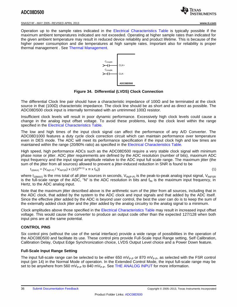
CLK+
CLK-
ADC08D500
Ccouple
Ccouple
ADC08D500
SNAS274F –MAY 2005–REVISED APRIL 2013 www.ti.com
Operation up to the sample rates indicated in the Electrical Characteristics Table is typically possible if themaximum ambient temperatures indicated are not exceeded. Operating at higher sample rates than indicated forthe given ambient temperature may result in reduced device reliability and product lifetime. This is because of thehigher power consumption and die temperatures at high sample rates. Important also for reliability is properthermal management . See Thermal Management.
Figure 34. Differential (LVDS) Clock Connection
The differential Clock line pair should have a characteristic impedance of 100Ω and be terminated at the clocksource in that (100Ω) characteristic impedance. The clock line should be as short and as direct as possible. TheADC08D500 clock input is internally terminated with an untrimmed 100Ω resistor.
Insufficient clock levels will result in poor dynamic performance. Excessively high clock levels could cause achange in the analog input offset voltage. To avoid these problems, keep the clock level within the rangespecified in the Electrical Characteristics Table.
The low and high times of the input clock signal can affect the performance of any A/D Converter. TheADC08D1000 features a duty cycle clock correction circuit which can maintain performance over temperatureeven in DES mode. The ADC will meet its performance specification if the input clock high and low times aremaintained within the range (20/80% ratio) as specified in the Electrical Characteristics Table.
High speed, high performance ADCs such as the ADC08D500 require a very stable clock signal with minimumphase noise or jitter. ADC jitter requirements are defined by the ADC resolution (number of bits), maximum ADCinput frequency and the input signal amplitude relative to the ADC input full scale range. The maximum jitter (thesum of the jitter from all sources) allowed to prevent a jitter-induced reduction in SNR is found to be
tJ(MAX) = (VIN(P-P) / VINFSR) x (1/(2(N+1) x π x fIN)) (1)
where tJ(MAX) is the rms total of all jitter sources in seconds, VIN(P-P) is the peak-to-peak analog input signal, VINFSRis the full-scale range of the ADC, "N" is the ADC resolution in bits and fIN is the maximum input frequency, inHertz, to the ADC analog input.
Note that the maximum jitter described above is the arithmetic sum of the jitter from all sources, including that inthe ADC clock, that added by the system to the ADC clock and input signals and that added by the ADC itself.Since the effective jitter added by the ADC is beyond user control, the best the user can do is to keep the sum ofthe externally added clock jitter and the jitter added by the analog circuitry to the analog signal to a minimum.
Clock amplitudes above those specified in the Electrical Characteristics Table may result in increased input offsetvoltage. This would cause the converter to produce an output code other than the expected 127/128 when bothinput pins are at the same potential.
CONTROL PINS
Six control pins (without the use of the serial interface) provide a wide range of possibilities in the operation ofthe ADC08D500 and facilitate its use. These control pins provide Full-Scale Input Range setting, Self Calibration,Calibration Delay, Output Edge Synchronization choice, LVDS Output Level choice and a Power Down feature.
Full-Scale Input Range Setting
The input full-scale range can be selected to be either 650 mVP-P or 870 mVP-P, as selected with the FSR controlinput (pin 14) in the Normal Mode of operation. In the Extended Control Mode, the input full-scale range may beset to be anywhere from 560 mVP-P to 840 mVP-P. See THE ANALOG INPUT for more information.
36 Submit Documentation Feedback Copyright © 2005–2013, Texas Instruments Incorporated
Product Folder Links: ADC08D500
ADC08D500
www.ti.com SNAS274F –MAY 2005–REVISED APRIL 2013
Self Calibration
The ADC08D500 self-calibration must be run to achieve specified performance. The calibration procedure is runupon power-up and can be run any time on command. The calibration procedure is exactly the same whetherthere is a clock present upon power up or if the clock begins some time after application of power. The CalRunoutput indicator is high while a calibration is in progress. Note that DCLK outputs are not active during acalibration cycle, therefore it is not recommended as a system clock.
Power-On Calibration
Power-on calibration begins after a time delay following the application of power. This time delay is determinedby the setting of CalDly, as described in the Calibration Delay Section, below.
The calibration process will be not be performed if the CAL pin is high at power up. In this case, the calibrationcycle will not begin until the on-command calibration conditions are met. The ADC08D500 will function with theCAL pin held high at power up, but no calibration will be done and performance will be impaired. A manualcalibration, however, may be performed after powering up with the CAL pin high. See On-Command Calibration.
The internal power-on calibration circuitry comes up in an unknown logic state. If the clock is not running atpower up and the power on calibration circuitry is active, it will hold the analog circuitry in power down and thepower consumption will typically be less than 200 mW. The power consumption will be normal after the clockstarts.
On-Command Calibration
An on-command calibration may be run at any time in NORMAL (non-DES) mode only. Do not run a calibrationwhile operating the ADC in Auto DES Mode.
If the ADC is operating in Auto DES mode and a calibration cycle is required then the controlling applicationshould bring the ADC into normal (non DES) mode before an On Command calibration is initiated. Oncecalibration has completed, the ADC can be put back into Auto DES mode.
To initiate an on-command calibration, bring the CAL pin high for a minimum of 80 input clock cycles after it hasbeen low for a minimum of 80 input clock cycles. Holding the CAL pin high upon power up will prevent executionof power-on calibration until the CAL pin is low for a minimum of 80 input clock cycles, then brought high for aminimum of another 80 input clock cycles. The calibration cycle will begin 80 input clock cycles after the CAL pinis thus brought high. The CalRun signal should be monitored to determine when the calibration cycle hascompleted. When an on-command calibration is executed, the CAL pin must be held low for 80 input clock cyclesand then low for 80 input clock cycles before the CalRun pin is activated to indicate that a calibration is takingplace. When the CalRun pin is activated, all outputs including the DCLK outputs are deactivated and enter a highimpedance state. After the calibration cycle is finished and the CalRun pin is low, the outputs, including DCLK,are active again but require a short settling period, typically around 100ns. Because the DCLK outputs are notactivated during a calibration cycle, they are not recommended for use as a system clock.
The minimum 80 input clock cycle sequences are required to ensure that random noise does not cause acalibration to begin when it is not desired. As mentioned in Self-Calibration for best performance, a selfcalibration should be performed 20 seconds or more after power up and repeated when the operatingtemperature changes significantly according to the particular system performance requirements. ENOB dropsslightly as junction temperature increases and executing a new self calibration cycle will essentially eliminate thechange.
Calibration Delay
The CalDly input (pin 127) is used to select one of two delay times after the application of power to the start ofcalibration, as described in Self-Calibration. The calibration delay values allow the power supply to come up andstabilize before calibration takes place. With no delay or insufficient delay, calibration would begin before thepower supply is stabilized at its operating value and result in non-optimal calibration coefficients. If the PD pin ishigh upon power-up, the calibration delay counter will be disabled until the PD pin is brought low. Therefore,holding the PD pin high during power up will further delay the start of the power-up calibration cycle. The bestsetting of the CalDly pin depends upon the power-on settling time of the power supply.
Note that the calibration delay selection is not possible in the Extended Control mode and the short delay time isused.
Copyright © 2005–2013, Texas Instruments Incorporated Submit Documentation Feedback 37
Product Folder Links: ADC08D500
ADC08D500
SNAS274F –MAY 2005–REVISED APRIL 2013 www.ti.com
Output Edge Synchronization
DCLK signals are available to help latch the converter output data into external circuitry. The output data can besynchronized with either edge of these clock signals. That is, the output data transition can be set to occur witheither the rising edge or the falling edge of the DCLK signal, so that either edge of that clock signal can be usedto latch the output data into the receiving circuit.
When OutEdge (pin 4) is high, the output data is synchronized with (changes with) the rising edge of the DCLK+(pin 82). When OutEdge is low, the output data is synchronized with the falling edge of DCLK+.
At the very high speeds of which the ADC08D500 is capable, slight differences in the lengths of the clock anddata lines can mean the difference between successful and erroneous data capture. The OutEdge pin is used tocapture data on the DCLK edge that best suits the application circuit and layout.
LVDS Output Level Control
The output level can be set to one of two levels with OutV (pin3). The strength of the output drivers is greaterwith OutV high. With OutV low there is less power consumption in the output drivers, but the lower output levelmeans decreased noise immunity.
For short LVDS lines and low noise systems, satisfactory performance may be realized with the FSR input low. Ifthe LVDS lines are long and/or the system in which the ADC08D500 is used is noisy, it may be necessary to tiethe FSR pin high.
Dual Edge Sampling
NOTEWhen using the ADC in Extended Control Mode, the Configuration Register must only bewritten when the DES Enable bit = 0. Writing to the Configuration Register when the DESEnable bit = 1 can cause the internal DES clock generation circuitry to stop.
The Dual Edge Sampling (DES) feature causes one of the two input pairs to be routed to both ADCs. The otherinput pair is deactivated. One of the ADCs samples the input signal on one clock edge, the other samples theinput signal on the other clock edge. The result is a 1:4 demultiplexed output with a sample rate that is twice theinput clock frequency.
To use this feature in the non-enhanced control mode, allow pin 127 to float and the signal at the "I" channelinput will be sampled by both converters. The Calibration Delay will then only be a short delay.
In the enhanced control mode, either input may be used for dual edge sampling. See Dual-Edge Sampling.
NOTE1) For the Extended Control Mode - When using the Automatic Clock Phase Controlfeature in dual edge sampling mode, it is important that the automatic phase control isdisabled (set bit 14 of DES Enable register Dh to 0) before the ADC is powered up. Notdoing so may cause the device not to wake up from the power down state.
2) For the Non-Extended Control Mode - When the ADC08D1000 is powered up and DESmode is required, ensure that pin 127 (CalDly/DES/SCS) is initially pulled low during orafter the power up sequence. The pin can then be allowed to float or be tied to VA / 2 toenter the DES mode. This will ensure that the part enters the DES mode correctly.
3) The automatic phase control should also be disabled if the input clock is interrupted orstopped for any reason. This is also the case if a large abrupt change in the clockfrequency occurs.
4) If a calibration of the ADC is required in Auto DES mode, the device must be returnedto the Normal Mode of operation before performing a calibration cycle. Once theCalibration has been completed, the device can be returned to the Auto DES mode andoperation can resume.
38 Submit Documentation Feedback Copyright © 2005–2013, Texas Instruments Incorporated
Product Folder Links: ADC08D500
ADC08D500
www.ti.com SNAS274F –MAY 2005–REVISED APRIL 2013
Power Down Feature
The Power Down pins (PD and PDQ) allow the ADC08D500 to be entirely powered down (PD) or the "Q"channel to be powered down and the "I" channel to remain active. See Power Down for details on the powerdown feature.
The digital data (+/-) output pins are put into a high impedance state when the PD pin for the respective channelis high. Upon return to normal operation, the pipeline will contain meaningless information and must be flushed.
If the PD input is brought high while a calibration is running, the device will not go into power down until thecalibration sequence is complete. However, if power is applied and PD is already high, the device will not beginthe calibration sequence until the PD input goes low. If a manual calibration is requested while the device ispowered down, the calibration will not begin at all. That is, the manual calibration input is completely ignored inthe power down state.
THE DIGITAL OUTPUTS
The ADC08D1000 demultiplexes the output data of each of the two ADCs on the die onto two LVDS outputbuses (total of four buses, two for each ADC). For each of the two converters, the results of successiveconversions started on the odd falling edges of the CLK+ pin are available on one of the two LVDS buses, whilethe results of conversions started on the even falling edges of the CLK+ pin are available on the other LVDS bus.This means that, the word rate at each LVDS bus is 1/2 the ADC08D1000 input clock rate and the two busesmust be multiplexed to obtain the entire 1 GSPS conversion result.
Since the minimum recommended input clock rate for this device is 200 MSPS (normal non DES mode), theeffective rate can be reduced to as low as 100 MSPS by using the results available on just one of the the twoLVDS buses and a 200 MHz input clock, decimating the 200 MSPS data by two.
There is one LVDS output clock pair (DCLK+/-) available for use to latch the LVDS outputs on all buses. Whetherthe data is sent at the rising or falling edge of DCLK is determined by the sense of the OutEdge pin, as describedin Output Edge Synchronization.
DDR (Double Data Rate) clocking can also be used. In this mode a word of data is presented with each edge ofDCLK, reducing the DCLK frequency to 1/4 the input clock frequency. See the Timing Diagram section fordetails.
The OutV pin is used to set the LVDS differential output levels. See LVDS Output Level Control.
The output format is Offset Binary. Accordingly, a full-scale input level with VIN+ positive with respect to VIN− willproduce an output code of all ones, a full-scale input level with VIN− positive with respect to VIN+ will produce anoutput code of all zeros and when VIN+ and VIN− are equal, the output code will vary between codes 127 and128.
POWER CONSIDERATIONS
A/D converters draw sufficient transient current to corrupt their own power supplies if not adequately bypassed. A33 µF capacitor should be placed within an inch (2.5 cm) of the A/D converter power pins. A 0.1 µF capacitorshould be placed as close as possible to each VA pin, preferably within one-half centimeter. Leadless chipcapacitors are preferred because they have low lead inductance.
The VA and VDR supply pins should be isolated from each other to prevent any digital noise from being coupledinto the analog portions of the ADC. A ferrite choke, such as the JW Miller FB20009-3B, is recommendedbetween these supply lines when a common source is used for them.
As is the case with all high speed converters, the ADC08D500 should be assumed to have little power supplynoise rejection. Any power supply used for digital circuitry in a system where a lot of digital power is beingconsumed should not be used to supply power to the ADC08D500. The ADC supplies should be the samesupply used for other analog circuitry, if not a dedicated supply.
Supply Voltage
The ADC08D500 is specified to operate with a supply voltage of 1.9V ±0.1V. It is very important to note that,while this device will function with slightly higher supply voltages, these higher supply voltages may reduceproduct lifetime.
Copyright © 2005–2013, Texas Instruments Incorporated Submit Documentation Feedback 39
Product Folder Links: ADC08D500
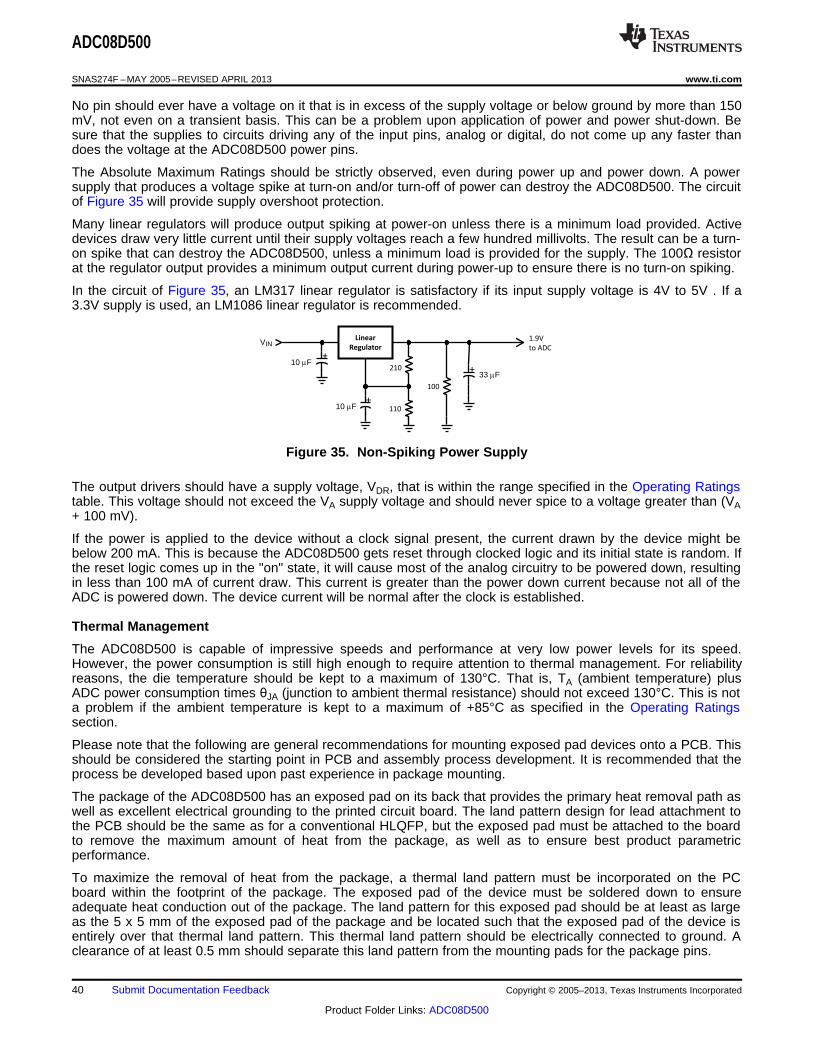
Linear
Regulator
210
110
100
+10 PF
+10 PF
VIN1.9V
to ADC
+33 PF
ADC08D500
SNAS274F –MAY 2005–REVISED APRIL 2013 www.ti.com
No pin should ever have a voltage on it that is in excess of the supply voltage or below ground by more than 150mV, not even on a transient basis. This can be a problem upon application of power and power shut-down. Besure that the supplies to circuits driving any of the input pins, analog or digital, do not come up any faster thandoes the voltage at the ADC08D500 power pins.
The Absolute Maximum Ratings should be strictly observed, even during power up and power down. A powersupply that produces a voltage spike at turn-on and/or turn-off of power can destroy the ADC08D500. The circuitof Figure 35 will provide supply overshoot protection.
Many linear regulators will produce output spiking at power-on unless there is a minimum load provided. Activedevices draw very little current until their supply voltages reach a few hundred millivolts. The result can be a turn-on spike that can destroy the ADC08D500, unless a minimum load is provided for the supply. The 100Ω resistorat the regulator output provides a minimum output current during power-up to ensure there is no turn-on spiking.
In the circuit of Figure 35, an LM317 linear regulator is satisfactory if its input supply voltage is 4V to 5V . If a3.3V supply is used, an LM1086 linear regulator is recommended.
Figure 35. Non-Spiking Power Supply
The output drivers should have a supply voltage, VDR, that is within the range specified in the Operating Ratingstable. This voltage should not exceed the VA supply voltage and should never spice to a voltage greater than (VA+ 100 mV).
If the power is applied to the device without a clock signal present, the current drawn by the device might bebelow 200 mA. This is because the ADC08D500 gets reset through clocked logic and its initial state is random. Ifthe reset logic comes up in the "on" state, it will cause most of the analog circuitry to be powered down, resultingin less than 100 mA of current draw. This current is greater than the power down current because not all of theADC is powered down. The device current will be normal after the clock is established.
Thermal Management
The ADC08D500 is capable of impressive speeds and performance at very low power levels for its speed.However, the power consumption is still high enough to require attention to thermal management. For reliabilityreasons, the die temperature should be kept to a maximum of 130°C. That is, TA (ambient temperature) plusADC power consumption times θJA (junction to ambient thermal resistance) should not exceed 130°C. This is nota problem if the ambient temperature is kept to a maximum of +85°C as specified in the Operating Ratingssection.
Please note that the following are general recommendations for mounting exposed pad devices onto a PCB. Thisshould be considered the starting point in PCB and assembly process development. It is recommended that theprocess be developed based upon past experience in package mounting.
The package of the ADC08D500 has an exposed pad on its back that provides the primary heat removal path aswell as excellent electrical grounding to the printed circuit board. The land pattern design for lead attachment tothe PCB should be the same as for a conventional HLQFP, but the exposed pad must be attached to the boardto remove the maximum amount of heat from the package, as well as to ensure best product parametricperformance.
To maximize the removal of heat from the package, a thermal land pattern must be incorporated on the PCboard within the footprint of the package. The exposed pad of the device must be soldered down to ensureadequate heat conduction out of the package. The land pattern for this exposed pad should be at least as largeas the 5 x 5 mm of the exposed pad of the package and be located such that the exposed pad of the device isentirely over that thermal land pattern. This thermal land pattern should be electrically connected to ground. Aclearance of at least 0.5 mm should separate this land pattern from the mounting pads for the package pins.
40 Submit Documentation Feedback Copyright © 2005–2013, Texas Instruments Incorporated
Product Folder Links: ADC08D500
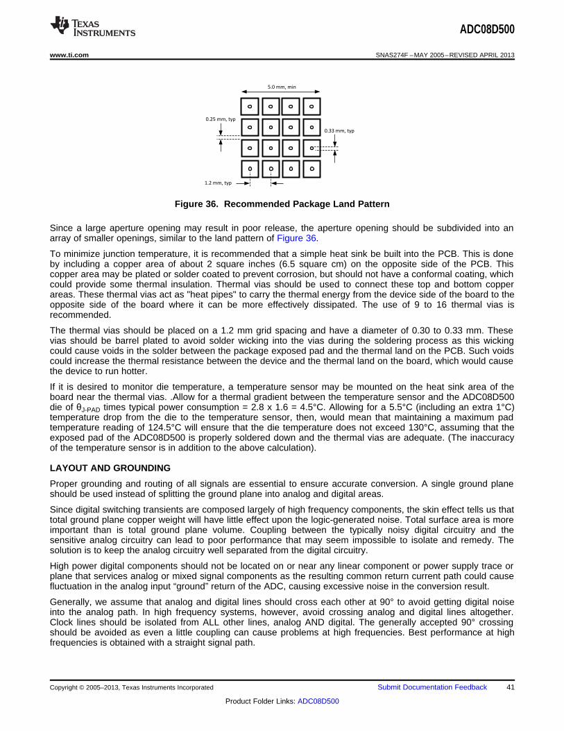
0.33 mm, typ
0.25 mm, typ
1.2 mm, typ
5.0 mm, min
ADC08D500
www.ti.com SNAS274F –MAY 2005–REVISED APRIL 2013
Figure 36. Recommended Package Land Pattern
Since a large aperture opening may result in poor release, the aperture opening should be subdivided into anarray of smaller openings, similar to the land pattern of Figure 36.
To minimize junction temperature, it is recommended that a simple heat sink be built into the PCB. This is doneby including a copper area of about 2 square inches (6.5 square cm) on the opposite side of the PCB. Thiscopper area may be plated or solder coated to prevent corrosion, but should not have a conformal coating, whichcould provide some thermal insulation. Thermal vias should be used to connect these top and bottom copperareas. These thermal vias act as "heat pipes" to carry the thermal energy from the device side of the board to theopposite side of the board where it can be more effectively dissipated. The use of 9 to 16 thermal vias isrecommended.
The thermal vias should be placed on a 1.2 mm grid spacing and have a diameter of 0.30 to 0.33 mm. Thesevias should be barrel plated to avoid solder wicking into the vias during the soldering process as this wickingcould cause voids in the solder between the package exposed pad and the thermal land on the PCB. Such voidscould increase the thermal resistance between the device and the thermal land on the board, which would causethe device to run hotter.
If it is desired to monitor die temperature, a temperature sensor may be mounted on the heat sink area of theboard near the thermal vias. .Allow for a thermal gradient between the temperature sensor and the ADC08D500die of θJ-PAD times typical power consumption = 2.8 x 1.6 = 4.5°C. Allowing for a 5.5°C (including an extra 1°C)temperature drop from the die to the temperature sensor, then, would mean that maintaining a maximum padtemperature reading of 124.5°C will ensure that the die temperature does not exceed 130°C, assuming that theexposed pad of the ADC08D500 is properly soldered down and the thermal vias are adequate. (The inaccuracyof the temperature sensor is in addition to the above calculation).
LAYOUT AND GROUNDING
Proper grounding and routing of all signals are essential to ensure accurate conversion. A single ground planeshould be used instead of splitting the ground plane into analog and digital areas.
Since digital switching transients are composed largely of high frequency components, the skin effect tells us thattotal ground plane copper weight will have little effect upon the logic-generated noise. Total surface area is moreimportant than is total ground plane volume. Coupling between the typically noisy digital circuitry and thesensitive analog circuitry can lead to poor performance that may seem impossible to isolate and remedy. Thesolution is to keep the analog circuitry well separated from the digital circuitry.
High power digital components should not be located on or near any linear component or power supply trace orplane that services analog or mixed signal components as the resulting common return current path could causefluctuation in the analog input “ground” return of the ADC, causing excessive noise in the conversion result.
Generally, we assume that analog and digital lines should cross each other at 90° to avoid getting digital noiseinto the analog path. In high frequency systems, however, avoid crossing analog and digital lines altogether.Clock lines should be isolated from ALL other lines, analog AND digital. The generally accepted 90° crossingshould be avoided as even a little coupling can cause problems at high frequencies. Best performance at highfrequencies is obtained with a straight signal path.
Copyright © 2005–2013, Texas Instruments Incorporated Submit Documentation Feedback 41
Product Folder Links: ADC08D500
ADC08D500
SNAS274F –MAY 2005–REVISED APRIL 2013 www.ti.com
The analog input should be isolated from noisy signal traces to avoid coupling of spurious signals into the input.This is especially important with the low level drive required of the ADC08D500. Any external component (e.g., afilter capacitor) connected between the converter's input and ground should be connected to a very clean point inthe analog ground plane. All analog circuitry (input amplifiers, filters, etc.) should be separated from any digitalcomponents.
DYNAMIC PERFORMANCE
The ADC08D500 is a.c. tested and its dynamic performance is specified. To meet the published specificationsand avoid jitter-induced noise, the clock source driving the CLK input must exhibit low rms jitter. The allowablejitter is a function of the input frequency and the input signal level, as described in THE CLOCK INPUTS.
It is good practice to keep the ADC clock line as short as possible, to keep it well away from any other signalsand to treat it as a transmission line. Other signals can introduce jitter into the clock signal. The clock signal canalso introduce noise into the analog path if not isolated from that path.
Best dynamic performance is obtained when the exposed pad at the back of the package has a good connectionto ground. This is because this path from the die to ground is a lower impedance than offered by the packagepins.
USING THE SERIAL INTERFACE
The ADC08D500 may be operated in the non-extended control (non-Serial Interface) mode or in the extendedcontrol mode. Table 14 and Table 15 describe the functions of pins 3, 4, 14 and 127 in the non-extended controlmode and the extended control mode, respectively.
Non-Extended Control Mode Operation
Non-extended control mode operation means that the Serial Interface is not active and all controllable functionsare controlled with various pin settings. That is, the full-scale range, single-ended or differential input and inputcoupling (a.c. or d.c.) are all controlled with pin settings. The non-extended control mode is used by setting pin14 high or low, as opposed to letting it float. Table 14 indicates the pin functions of the ADC08D500 in the non-extended control mode.
Table 14. Non-Extended Control Mode Operation(Pin 14 High or Low)
Pin Low High Floating
3 0.51 VP-P Output 0.71 VP-P Output n/a
4 OutEdge = Neg OutEdge = Pos DDR
127 CalDly Low CalDly High DES
14 650 mVP-P input range 870 mVP-P input range Extended Control Mode
Pin 3 can be either high or low in the non-extended control mode. Pin 14 must not be left floating to select thismode. See NORMAL/EXTENDED CONTROL for more information.
Pin 4 can be high or low or can be left floating in the non-extended control mode. In the non-extended controlmode, pin 4 high or low defines the edge at which the output data transitions. See Output Edge Synchronizationfor more information. If this pin is floating, the output clock (DCLK) is a DDR (Double Data Rate) clock (seeDouble Data Rate) and the output edge synchronization is irrelevant since data is clocked out on both DCLKedges.
Pin 127, if it is high or low in the non-extended control mode, sets the calibration delay. If pin 127 is floating, thecalibration delay is the same as it would be with this pin low and the converter performs dual edge sampling(DES).
Table 15. Extended Control Mode Operation(Pin 14 Floating)
Pin Function
3 SCLK (Serial Clock)
4 SDATA (Serial Data)
42 Submit Documentation Feedback Copyright © 2005–2013, Texas Instruments Incorporated
Product Folder Links: ADC08D500
ADC08D500
www.ti.com SNAS274F –MAY 2005–REVISED APRIL 2013
Table 15. Extended Control Mode Operation(Pin 14 Floating) (continued)
Pin Function
127 SCS (Serial Interface Chip Select)
COMMON APPLICATION PITFALLS
Failure to write all register locations when using extended control mode. When using the serial interface, all8 user registers must be written at least once with the default or desired values before calibration andsubsequent use of the ADC. In addition, the first write to the DES Enable register (Dh) must load the defaultvalue (0x3FFFh). Once all registers have been written once, other desired settings, including enabling DES canbe loaded.
Driving the inputs (analog or digital) beyond the power supply rails. For device reliability, no input shouldnot go more than 150 mV below the ground pins or 150 mV above the supply pins. Exceeding these limits oneven a transient basis may not only cause faulty or erratic operation, but may impair device reliability. It is notuncommon for high speed digital circuits to exhibit undershoot that goes more than a volt below ground.Controlling the impedance of high speed lines and terminating these lines in their characteristic impedanceshould control overshoot.
Care should be taken not to overdrive the inputs of the ADC08D500. Such practice may lead to conversioninaccuracies and even to device damage.
Incorrect analog input common mode voltage in the d.c. coupled mode. As discussed in The Analog Inputsand THE ANALOG INPUT, the Input common mode voltage must remain within 50 mV of the VCMO output, whichhas a variability with temperature that must also be tracked. Distortion performance will be degraded if the inputcommon mode voltage is more than 50 mV from VCMO .
Using an inadequate amplifier to drive the analog input. Use care when choosing a high frequency amplifierto drive the ADC08D500 as many high speed amplifiers will have higher distortion than will the ADC08D500,resulting in overall system performance degradation.
Driving the VBG pin to change the reference voltage. As mentioned in THE REFERENCE VOLTAGE, thereference voltage is intended to be fixed to provide one of two different full-scale values (650 mVP-P and 870mVP-P). Over driving this pin will not change the full scale value, but can otherwise upset operation.
Driving the clock input with an excessively high level signal. The ADC clock level should not exceed thelevel described in the Operating Ratings Table or the input offset could change.
Inadequate clock levels. As described in THE CLOCK INPUTS, insufficient clock levels can result in poorperformance. Excessive clock levels could result in the introduction of an input offset.
Using a clock source with excessive jitter, using an excessively long clock signal trace, or having othersignals coupled to the clock signal trace. This will cause the sampling interval to vary, causing excessiveoutput noise and a reduction in SNR performance.
Failure to provide adequate heat removal. As described in Thermal Management, it is important to provideadequate heat removal to ensure device reliability. This can either be done with adequate air flow or the use of asimple heat sink built into the board. The backside pad should be grounded for best performance.
Copyright © 2005–2013, Texas Instruments Incorporated Submit Documentation Feedback 43
Product Folder Links: ADC08D500
ADC08D500
SNAS274F –MAY 2005–REVISED APRIL 2013 www.ti.com
REVISION HISTORY
Changes from Revision E (April 2013) to Revision F Page
• Changed layout of National Data Sheet to TI format .......................................................................................................... 43
44 Submit Documentation Feedback Copyright © 2005–2013, Texas Instruments Incorporated
Product Folder Links: ADC08D500
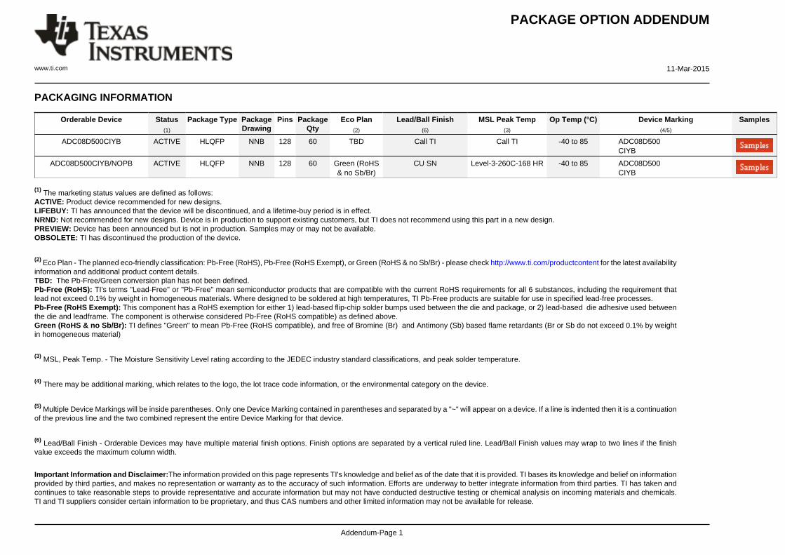
PACKAGE OPTION ADDENDUM
www.ti.com 11-Mar-2015
Addendum-Page 1
PACKAGING INFORMATION
Orderable Device Status(1)
Package Type PackageDrawing
Pins PackageQty
Eco Plan(2)
Lead/Ball Finish(6)
MSL Peak Temp(3)
Op Temp (°C) Device Marking(4/5)
Samples
ADC08D500CIYB ACTIVE HLQFP NNB 128 60 TBD Call TI Call TI -40 to 85 ADC08D500CIYB
ADC08D500CIYB/NOPB ACTIVE HLQFP NNB 128 60 Green (RoHS& no Sb/Br)
CU SN Level-3-260C-168 HR -40 to 85 ADC08D500CIYB
(1) The marketing status values are defined as follows:ACTIVE: Product device recommended for new designs.LIFEBUY: TI has announced that the device will be discontinued, and a lifetime-buy period is in effect.NRND: Not recommended for new designs. Device is in production to support existing customers, but TI does not recommend using this part in a new design.PREVIEW: Device has been announced but is not in production. Samples may or may not be available.OBSOLETE: TI has discontinued the production of the device.
(2) Eco Plan - The planned eco-friendly classification: Pb-Free (RoHS), Pb-Free (RoHS Exempt), or Green (RoHS & no Sb/Br) - please check http://www.ti.com/productcontent for the latest availabilityinformation and additional product content details.TBD: The Pb-Free/Green conversion plan has not been defined.Pb-Free (RoHS): TI's terms "Lead-Free" or "Pb-Free" mean semiconductor products that are compatible with the current RoHS requirements for all 6 substances, including the requirement thatlead not exceed 0.1% by weight in homogeneous materials. Where designed to be soldered at high temperatures, TI Pb-Free products are suitable for use in specified lead-free processes.Pb-Free (RoHS Exempt): This component has a RoHS exemption for either 1) lead-based flip-chip solder bumps used between the die and package, or 2) lead-based die adhesive used betweenthe die and leadframe. The component is otherwise considered Pb-Free (RoHS compatible) as defined above.Green (RoHS & no Sb/Br): TI defines "Green" to mean Pb-Free (RoHS compatible), and free of Bromine (Br) and Antimony (Sb) based flame retardants (Br or Sb do not exceed 0.1% by weightin homogeneous material)
(3) MSL, Peak Temp. - The Moisture Sensitivity Level rating according to the JEDEC industry standard classifications, and peak solder temperature.
(4) There may be additional marking, which relates to the logo, the lot trace code information, or the environmental category on the device.
(5) Multiple Device Markings will be inside parentheses. Only one Device Marking contained in parentheses and separated by a "~" will appear on a device. If a line is indented then it is a continuationof the previous line and the two combined represent the entire Device Marking for that device.
(6) Lead/Ball Finish - Orderable Devices may have multiple material finish options. Finish options are separated by a vertical ruled line. Lead/Ball Finish values may wrap to two lines if the finishvalue exceeds the maximum column width.
Important Information and Disclaimer:The information provided on this page represents TI's knowledge and belief as of the date that it is provided. TI bases its knowledge and belief on informationprovided by third parties, and makes no representation or warranty as to the accuracy of such information. Efforts are underway to better integrate information from third parties. TI has taken andcontinues to take reasonable steps to provide representative and accurate information but may not have conducted destructive testing or chemical analysis on incoming materials and chemicals.TI and TI suppliers consider certain information to be proprietary, and thus CAS numbers and other limited information may not be available for release.
PACKAGE OPTION ADDENDUM
www.ti.com 11-Mar-2015
Addendum-Page 2
In no event shall TI's liability arising out of such information exceed the total purchase price of the TI part(s) at issue in this document sold by TI to Customer on an annual basis.
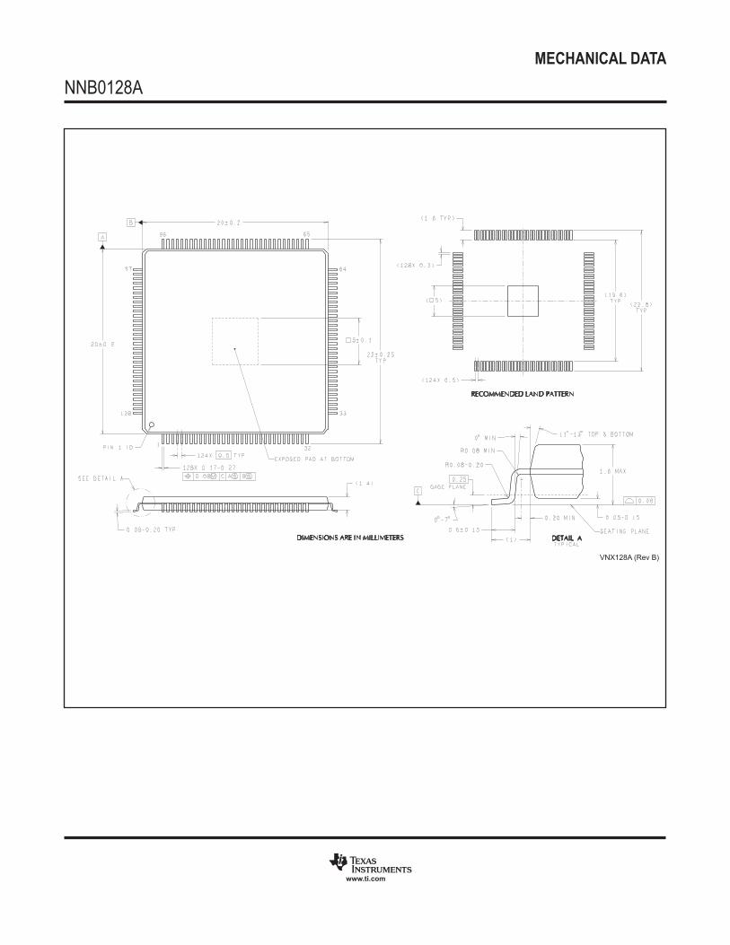
MECHANICAL DATA
NNB0128A
www.ti.com
VNX128A (Rev B)
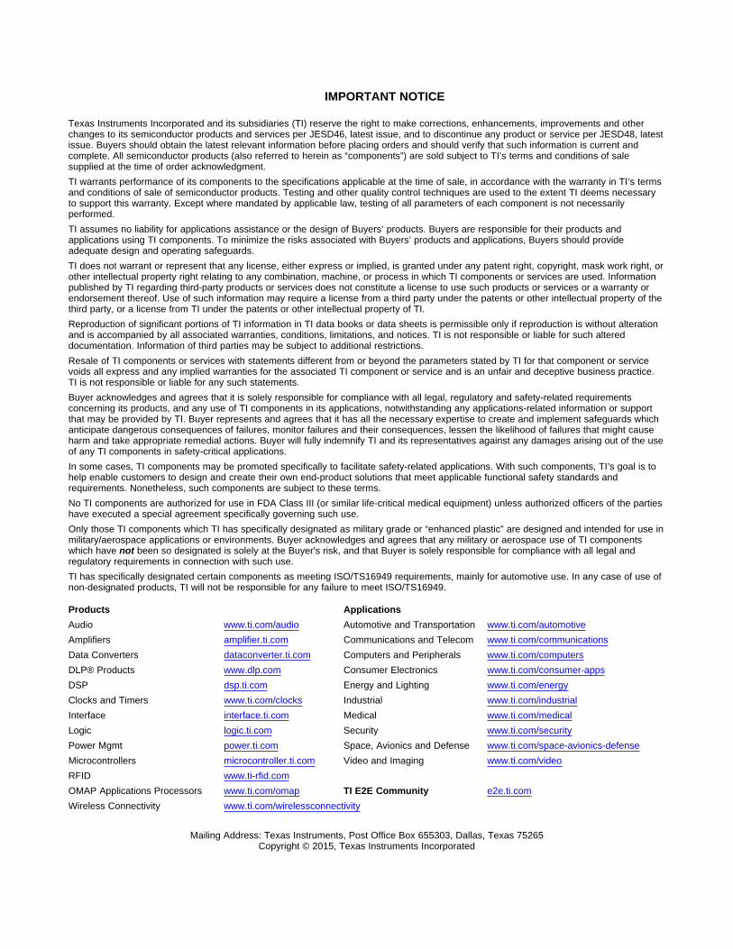
IMPORTANT NOTICE
Texas Instruments Incorporated and its subsidiaries (TI) reserve the right to make corrections, enhancements, improvements and otherchanges to its semiconductor products and services per JESD46, latest issue, and to discontinue any product or service per JESD48, latestissue. Buyers should obtain the latest relevant information before placing orders and should verify that such information is current andcomplete. All semiconductor products (also referred to herein as “components”) are sold subject to TI’s terms and conditions of salesupplied at the time of order acknowledgment.TI warrants performance of its components to the specifications applicable at the time of sale, in accordance with the warranty in TI’s termsand conditions of sale of semiconductor products. Testing and other quality control techniques are used to the extent TI deems necessaryto support this warranty. Except where mandated by applicable law, testing of all parameters of each component is not necessarilyperformed.TI assumes no liability for applications assistance or the design of Buyers’ products. Buyers are responsible for their products andapplications using TI components. To minimize the risks associated with Buyers’ products and applications, Buyers should provideadequate design and operating safeguards.TI does not warrant or represent that any license, either express or implied, is granted under any patent right, copyright, mask work right, orother intellectual property right relating to any combination, machine, or process in which TI components or services are used. Informationpublished by TI regarding third-party products or services does not constitute a license to use such products or services or a warranty orendorsement thereof. Use of such information may require a license from a third party under the patents or other intellectual property of thethird party, or a license from TI under the patents or other intellectual property of TI.Reproduction of significant portions of TI information in TI data books or data sheets is permissible only if reproduction is without alterationand is accompanied by all associated warranties, conditions, limitations, and notices. TI is not responsible or liable for such altereddocumentation. Information of third parties may be subject to additional restrictions.Resale of TI components or services with statements different from or beyond the parameters stated by TI for that component or servicevoids all express and any implied warranties for the associated TI component or service and is an unfair and deceptive business practice.TI is not responsible or liable for any such statements.Buyer acknowledges and agrees that it is solely responsible for compliance with all legal, regulatory and safety-related requirementsconcerning its products, and any use of TI components in its applications, notwithstanding any applications-related information or supportthat may be provided by TI. Buyer represents and agrees that it has all the necessary expertise to create and implement safeguards whichanticipate dangerous consequences of failures, monitor failures and their consequences, lessen the likelihood of failures that might causeharm and take appropriate remedial actions. Buyer will fully indemnify TI and its representatives against any damages arising out of the useof any TI components in safety-critical applications.In some cases, TI components may be promoted specifically to facilitate safety-related applications. With such components, TI’s goal is tohelp enable customers to design and create their own end-product solutions that meet applicable functional safety standards andrequirements. Nonetheless, such components are subject to these terms.No TI components are authorized for use in FDA Class III (or similar life-critical medical equipment) unless authorized officers of the partieshave executed a special agreement specifically governing such use.Only those TI components which TI has specifically designated as military grade or “enhanced plastic” are designed and intended for use inmilitary/aerospace applications or environments. Buyer acknowledges and agrees that any military or aerospace use of TI componentswhich have not been so designated is solely at the Buyer's risk, and that Buyer is solely responsible for compliance with all legal andregulatory requirements in connection with such use.TI has specifically designated certain components as meeting ISO/TS16949 requirements, mainly for automotive use. In any case of use ofnon-designated products, TI will not be responsible for any failure to meet ISO/TS16949.
Products ApplicationsAudio www.ti.com/audio Automotive and Transportation www.ti.com/automotiveAmplifiers amplifier.ti.com Communications and Telecom www.ti.com/communicationsData Converters dataconverter.ti.com Computers and Peripherals www.ti.com/computersDLP® Products www.dlp.com Consumer Electronics www.ti.com/consumer-appsDSP dsp.ti.com Energy and Lighting www.ti.com/energyClocks and Timers www.ti.com/clocks Industrial www.ti.com/industrialInterface interface.ti.com Medical www.ti.com/medicalLogic logic.ti.com Security www.ti.com/securityPower Mgmt power.ti.com Space, Avionics and Defense www.ti.com/space-avionics-defenseMicrocontrollers microcontroller.ti.com Video and Imaging www.ti.com/videoRFID www.ti-rfid.comOMAP Applications Processors www.ti.com/omap TI E2E Community e2e.ti.comWireless Connectivity www.ti.com/wirelessconnectivity
Mailing Address: Texas Instruments, Post Office Box 655303, Dallas, Texas 75265Copyright © 2015, Texas Instruments Incorporated


![Atmel ATmega16U4, ATmega32U4 Datasheet …...ATmega16U4/32U4 [DATASHEET] 8](https://static.fdocuments.us/doc/165x107/5f0a39897e708231d42a9d86/-atmel-atmega16u4-atmega32u4-datasheet-atmega16u432u4-datasheet-8.jpg)
