Adaptive Voltage Management Enabling Energy E … · Adaptive Voltage Management Enabling Energy...
165
Adaptive Voltage Management Enabling Energy Efficiency in Nanoscale Integrated Circuits by Alexander E. Shapiro Submitted in Partial Fulfillment of the Requirements for the Degree Doctor of Philosophy Supervised by Professor Eby G. Friedman Department of Electrical and Computer Engineering Arts, Sciences and Engineering Edmund A. Hajim School of Engineering and Applied Sciences University of Rochester Rochester, New York 2016
Transcript of Adaptive Voltage Management Enabling Energy E … · Adaptive Voltage Management Enabling Energy...
Adaptive Voltage Management Enabling Energy
Efficiency in Nanoscale Integrated Circuits
by
Alexander E. Shapiro
Submitted in Partial Fulfillment
of the
Requirements for the Degree
Doctor of Philosophy
Supervised by
Professor Eby G. Friedman
Department of Electrical and Computer Engineering
Arts, Sciences and Engineering
Edmund A. Hajim School of Engineering and Applied Sciences
University of Rochester
Rochester, New York
2016

ii
Dedication
This work is dedicated to my parents, Irina and Evgeny Shapiro.

iii
Biographical Sketch
Alexander Shapiro was born in Moscow, Russia. He
received his Bachelor of Science degree in Computer En-
gineering from the Technion–Israel Institute of Tech-
nology, Haifa, Israel, in 2011, and Master of Science
degree in Electrical Engineering from the University of
Rochester, Rochester, New York, in 2013.
Between 2008 and 2011, he held a variety of software and hardware Research and
Development positions at IBM and Intel in Israel. Alexander was employed as an
intern in the Circuits Design Group at Qualcomm, North Carolina in summer 2013
and in the Memory IP group at Intel, Oregon in summer 2015. His current research
interests include the analysis and design of high performance integrated circuits, low
power design techniques, and near threshold circuits.
iv
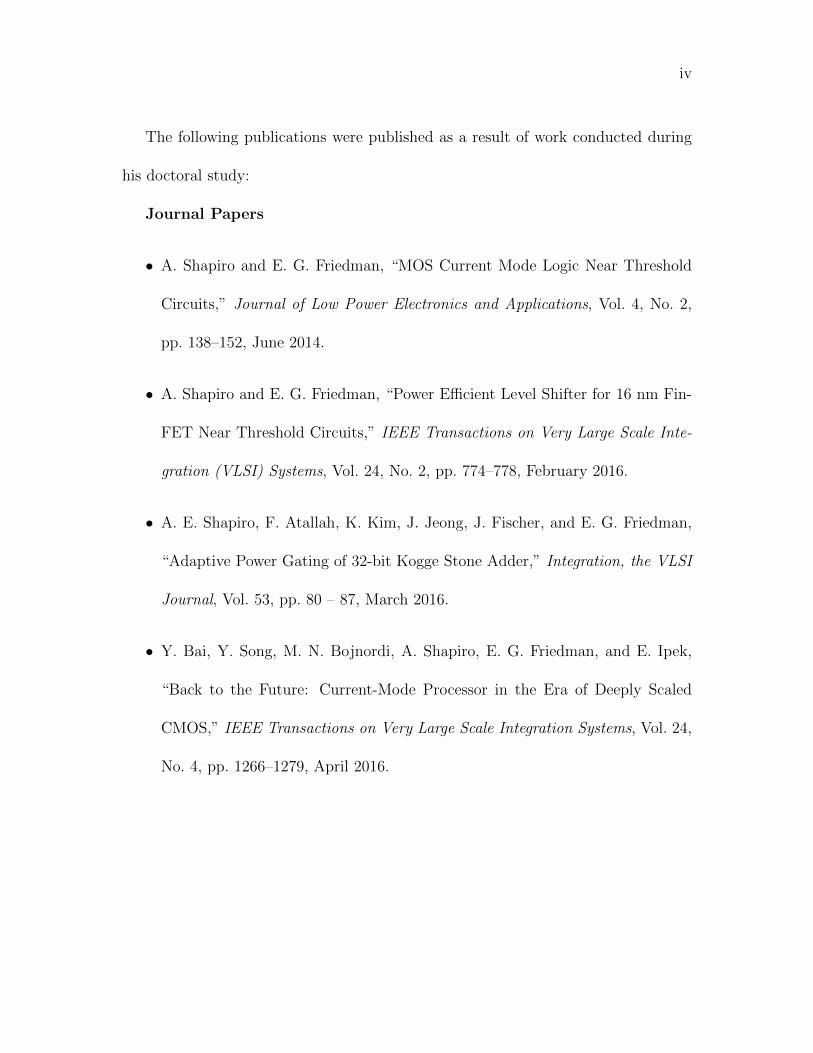
The following publications were published as a result of work conducted during
his doctoral study:
Journal Papers
• A. Shapiro and E. G. Friedman, “MOS Current Mode Logic Near Threshold
Circuits,” Journal of Low Power Electronics and Applications, Vol. 4, No. 2,
pp. 138–152, June 2014.
• A. Shapiro and E. G. Friedman, “Power Efficient Level Shifter for 16 nm Fin-
FET Near Threshold Circuits,” IEEE Transactions on Very Large Scale Inte-
gration (VLSI) Systems, Vol. 24, No. 2, pp. 774–778, February 2016.
• A. E. Shapiro, F. Atallah, K. Kim, J. Jeong, J. Fischer, and E. G. Friedman,
“Adaptive Power Gating of 32-bit Kogge Stone Adder,” Integration, the VLSI
Journal, Vol. 53, pp. 80 – 87, March 2016.
• Y. Bai, Y. Song, M. N. Bojnordi, A. Shapiro, E. G. Friedman, and E. Ipek,
“Back to the Future: Current-Mode Processor in the Era of Deeply Scaled
CMOS,” IEEE Transactions on Very Large Scale Integration Systems, Vol. 24,
No. 4, pp. 1266–1279, April 2016.
v
• A. Shapiro and E. G. Friedman, “Interconnect Delay Model for Wide Supply
Voltage Range Repeater Insertion in Sub-22 nm FinFET Technologies,” IEEE
Transactions on Very Large Scale Integration Systems (under review)
Conference Papers
• A. Shapiro and E. G. Friedman, “Performance Characteristics of 14 nm Near
Threshold MCML Circuits,” Proceedings of the IEEE SOI-3D-Subthreshold Mi-
croelectronics Technology Unified Conference, pp. 79–80, October 2013.
• A. Shapiro and E. G. Friedman, “Power Efficiency of 14 nm MCML Near
Threshold Circuits,” Proceedings of the 37th Annual IEEE EDS/CAS Activities
in Western New York Conference, p. 16, November 2013.
• Y. Bai, Y. Song, M. N. Bojnordi, A. Shapiro, E. Ipek, and E. G. Friedman, “Ar-
chitecting a MOS Current Mode Logic (MCML) Processor for Fast, Low Noise
and Energy-Efficient Computing in the Near-Threshold Regime,” Proceedings
of the IEEE International Conference on Computer Design, pp. 527–534, Oc-
tober 2015.

vi
Acknowledgements
My experience at the University of Rochester has been unparalleled to any other
experience in my life. I signed up for a PhD, and in return I was gifted with an
incredible academic advisor and mentor, friends, and colleagues who have pushed and
challenged my professional and personal beliefs. I have stretched myself intellectually
and emotionally. For this, I would like to thank all of the individuals who have played
an exceptionally formative role in my development.
First and foremost, I would like to give special thanks to my advisor Professor
Eby G. Friedman for his extraordinary investment of time, effort, and belief. With
his guidance, I developed a new appreciation for very large scale integrated circuits.
Something that was once monotonous and routine, a mere job responsibility, was now
a subject of study. Academic research unveiled the many questions and challenges
teaching me to think critically about my work. A take away that in and of itself has
been worth all of my time during this PhD experience.

vii
I would also like to thank the members of my committee, Professors Engin Ipek,
Paul Ampadu, Chen Ding, and my committee chair, Professor Harry Groenvelt, for
serving on my proposal and defense committees. Thank you for fruitful discussions
and comments during my proposal and defense. Thank you to the University of
Rochester, and specifically, the Department of Electrical and Computer Engineer-
ing for affording a faculty rich in knowledge and experience who have all played an
integral role in my intellectual and professional development. Thanks to Professor
Engin Ipek and Yuxin Bai for an opportunity to collaborate on a novel high perfor-
mance technology. This collaboration contributed to my technical development and
expanded my professional experience.
I would also like to thank Jeff Fischer, Francois Atallah, Kyungseok Kim, Jihoon
Jeong for the opportunity to collaborate with Qualcomm, and especially Burt Price
of Qualcomm for his insights and technical discussions. Thanks to Pavel Rott for
guiding me to excel during my summer internship at Intel. He consistently challenged
me to complete a variety of projects that put my analytic skills to the test, and
consequently, further helped refine my engineering skills. Thank you for taking
the time and effort to make my internship at Intel beneficial both for my personal
development and the company.

viii
I am grateful to members of the High Performance VLSI/IC Design and Analysis
Laboratory: Boris Vaisband, Ravi Patel, Mohammad Kazemi, Shen Ge, Kan Xu,
Albert Ciprut, Ange Maurice, and Nathan Kistner. Your support has been tremen-
dous and I value the privilege of calling you my friends and colleagues. With special
thanks to Dr. Inna Vaisband for enabling this extraordinary experience and helping
me throughout the PhD program with personal and technical advice. I also want to
thank RuthAnn Williams for her friendship and constant help with all administrative
tasks. Her baked goods supplied the energy that drove my intellectual achievements.
Many thanks to my network of friends and relatives from Russia and Israel who have
provided moral support, motivation, and encouragement as I transitioned across the
world to embark on this important chapter of my life.
Finally, I want to extend special thanks to my wife, my in-laws, my sister, and my
parents for providing me with emotional support and encouragement and consistently
believing in me in those moments when I did not believe in myself. Without them,
this PhD would not be possible.
This experience filled my life with very important people and very formative
memories. For this, I am forever grateful to Professor Eby G. Friedman and the
University of Rochester.
ix
Abstract
Battery powered devices emphasize energy efficiency in modern sub-22 nm CMOS
microprocessors rendering classic power reduction solutions not sufficient. Classical
solutions that reduce power consumption in high performance integrated circuits are
superseded with novel and enhanced power reduction techniques to enable the greater
energy efficiency desired in modern microprocessors and emerging mobile platforms.
Dynamic power consumption is reduced by operating over a wide range of supply
voltages. This region of operation is enabled by a high speed and power efficient level
shifter which translates low voltage digital signals to higher voltages (and vice versa),
a key component that enables communication among circuits operating at different
voltage levels. Additionally, optimizing the wide supply voltage range of signals
propagating across long interconnect enables greater energy savings. A closed-form
delay model supporting wide voltage range is developed to enable this capability. The
model supports an ultra-wide voltage range from nominal voltages to subthreshold

x
voltages, and a wide range of repeater sizes. To mitigate the drawback of lower
operating speed at reduced supply voltages, the high performance exhibited by MOS
current mode logic technology is exploited. High performance and energy efficient
circuits are enabled by combining this logic style with power efficient near threshold
circuits. Many-core systems that operate at high frequencies and process highly
parallel workloads benefit from this combination of MCML with NTC.
Due to aggressive scaling, static power consumption can in some cases overshadow
dynamic power. Techniques to lower leakage power have therefore become an impor-
tant objective in modern microprocessors. To address this issue, an adaptive power
gating technique is proposed. This technique utilizes high levels of granularity to
save additional leakage power when a circuit is active as opposed to standard power
gating that saves static power only when the entire circuit is powered off. This tech-
nique provides significant savings in static power in addition to standard benefits
from classical power gating.
Improvements in energy efficiency are enabled by reducing both static and dy-
namic power consumption utilizing adaptive and near threshold circuit techniques.
These advanced power reduction techniques will enable the greater energy efficiency
required in modern portable systems.
xi
Contributors and Funding Sources
The research presented in this dissertation is supervised by a committee consisting
of Professors Eby G. Friedman (advisor), Engin Ipek, and Paul Ampadu of the
Department of Electrical and Computer Engineering, as well as Professor Chen Ding
of the Department of Computer Science. The committee is chaired by Professor
Harry Groenevelt of the Operations Management of the Simon Business School.
The author developed novel and advanced low power circuits and design techniques
to enable the greater power savings required in modern applications. Chapters 1
and 2 comprise introductory material based on the literature published by other
researchers. The contributions of the co-authors are described below for each chapter.
Chapter 3: Alexander Shapiro is the principal author of the chapter contributing
the circuit design, circuit performance evaluation, and layout. The research and
evaluation are supported by E. G. Friedman. The results are published in the IEEE
Transactions on Very Large Scale Integration (VLSI) Systems.
xii
Chapter 4: Alexander Shapiro is the principal author of this chapter, contributing
the novel circuit technique combining MCML with NTC, circuit simulation, and
energy efficiency evaluation. The research and evaluation are supported by E. G.
Friedman. The results from this study are published in the Journal of Low Power
Electronics and Applications.
Chapter 5: Alexander Shapiro is the principal author of this chapter, provid-
ing the adaptive power gating application, circuit simulations, and energy efficiency
evaluation. The development of this research was performed in collaboration with
co-authors F. Atallah, K. Kim, J. Jeong, J. Fischer, and E. G. Friedman. The results
are published in Integration, the VLSI Journal.
Chapter 6: Alexander Shapiro is the principal author of this chapter, contribut-
ing the wide voltage range interconnect delay model, wide voltage range repeater
insertion, and circuit simulations. The research and evaluation are supported by E.
G. Friedman. The results have been submitted to the IEEE Transactions on Very
Large Scale Integration (VLSI) Systems.
Chapters 7 and 8: The concluding and future work chapters are written by
Alexander Shapiro with support from E. G. Friedman.
This graduate work was supported by a Dean’s Fellowship from the University
of Rochester and by grants from the Binational Science Foundation under Grant

xiii
No. 2012139, the National Science Foundation under Grant Nos. CCF-1329374,
CCF-1526466, and CNS-1548078, IARPA under Grant No. W911NF-14-C-0089,
and by grants from Intel Corporation, Samsung Electronics, Cisco Corporation, and
Qualcomm Corporation.

xiv
Table of Contents
Dedication ii
Biographical Sketch iii
Acknowledgements vi
Abstract ix
Contributors and Funding Sources xi
List of Tables xix
List of Figures xx
1 Introduction 1
1.1 Low power circuits and techniques . . . . . . . . . . . . . . . . . . . . 5
1.2 Outline . . . . . . . . . . . . . . . . . . . . . . . . . . . . . . . . . . . 8

xv
2 Power consumption and reduction techniques in CMOS circuits 11
2.1 Dynamic power component . . . . . . . . . . . . . . . . . . . . . . . . 12
2.1.1 Subthreshold circuits . . . . . . . . . . . . . . . . . . . . . . . 15
2.1.2 Near threshold circuits . . . . . . . . . . . . . . . . . . . . . . 19
2.1.3 Advanced near threshold circuits . . . . . . . . . . . . . . . . 22
2.2 Short-circuit power component . . . . . . . . . . . . . . . . . . . . . . 25
2.3 Leakage power component . . . . . . . . . . . . . . . . . . . . . . . . 27
2.3.1 Power gating . . . . . . . . . . . . . . . . . . . . . . . . . . . 29
2.4 Summary . . . . . . . . . . . . . . . . . . . . . . . . . . . . . . . . . 31
3 Power efficient level shifter for 16 nm FinFET near threshold cir-
cuits 34
3.1 Previous work . . . . . . . . . . . . . . . . . . . . . . . . . . . . . . . 35
3.1.1 Standard level shifter . . . . . . . . . . . . . . . . . . . . . . . 35
3.1.2 Advanced level shifter . . . . . . . . . . . . . . . . . . . . . . 37
3.2 Proposed wide voltage range level shifter for near threshold circuits . 39
3.2.1 Structure of the proposed wide voltage range level shifter . . . 39
3.2.2 Example of operation . . . . . . . . . . . . . . . . . . . . . . . 43
3.3 Evaluation of proposed level shifter . . . . . . . . . . . . . . . . . . . 44
3.3.1 Simulation setup . . . . . . . . . . . . . . . . . . . . . . . . . 45
xvi
3.3.2 Simulation results . . . . . . . . . . . . . . . . . . . . . . . . . 46
3.3.3 Comparison to previous works . . . . . . . . . . . . . . . . . . 49
3.4 Summary . . . . . . . . . . . . . . . . . . . . . . . . . . . . . . . . . 50
4 Interconnect Model for Wide Supply Voltage Range Repeater In-
sertion 51
4.1 Existing FinFET transistor and Interconnect Delay Models . . . . . . 56
4.2 Single stage delay in wide supply voltage range applications . . . . . 58
4.3 Interconnect delay model . . . . . . . . . . . . . . . . . . . . . . . . . 62
4.4 Repeater insertion for wide supply voltage range applications . . . . . 63
4.4.1 Optimal number of repeaters across a range of supply voltages 63
4.4.2 Effect on delay of a fixed number of repeaters . . . . . . . . . 65
4.4.3 Maximum supply voltage range with delay constraint . . . . . 66
4.5 Summary . . . . . . . . . . . . . . . . . . . . . . . . . . . . . . . . . 68
5 MOS current mode logic near threshold circuits 69
5.1 Background . . . . . . . . . . . . . . . . . . . . . . . . . . . . . . . . 70
5.1.1 MCML circuits . . . . . . . . . . . . . . . . . . . . . . . . . . 70
5.2 Combination of MCML and NTC . . . . . . . . . . . . . . . . . . . . 76
5.2.1 MCML with NTC . . . . . . . . . . . . . . . . . . . . . . . . 77

xvii
5.2.2 Sensitivity to process variation of MCML with NTC . . . . . . 79
5.2.3 Characterization of basic MCML with NTC gates . . . . . . . 81
5.3 Simulation setup . . . . . . . . . . . . . . . . . . . . . . . . . . . . . 82
5.3.1 Description of test circuit . . . . . . . . . . . . . . . . . . . . 82
5.3.2 Power simulation setup . . . . . . . . . . . . . . . . . . . . . . 84
5.3.3 Noise simulation setup . . . . . . . . . . . . . . . . . . . . . . 85
5.4 Simulation results . . . . . . . . . . . . . . . . . . . . . . . . . . . . . 86
5.4.1 Power/speed . . . . . . . . . . . . . . . . . . . . . . . . . . . . 86
5.4.2 Noise . . . . . . . . . . . . . . . . . . . . . . . . . . . . . . . . 88
5.5 Summary . . . . . . . . . . . . . . . . . . . . . . . . . . . . . . . . . 89
6 Adaptive power gating application of 32-bit adder at 16 nm FinFET
technology node 91
6.1 32-bit Kogge Stone adder structure . . . . . . . . . . . . . . . . . . . 93
6.2 Adaptive power gating of 32-bit Kogge Stone adder . . . . . . . . . . 94
6.2.1 Power switches . . . . . . . . . . . . . . . . . . . . . . . . . . 95
6.2.2 Isolation cells . . . . . . . . . . . . . . . . . . . . . . . . . . . 97
6.2.3 Controller . . . . . . . . . . . . . . . . . . . . . . . . . . . . . 98
6.2.4 Optimal cluster size with shared power switches . . . . . . . . 101
6.3 Evaluation and results . . . . . . . . . . . . . . . . . . . . . . . . . . 105

xviii
6.3.1 Simple adaptive controller . . . . . . . . . . . . . . . . . . . . 107
6.3.2 Comparison of the simple adaptive power gating technique to
standard power gating approach . . . . . . . . . . . . . . . . . 110
6.3.3 Enhanced adaptive controller . . . . . . . . . . . . . . . . . . 112
6.4 Summary . . . . . . . . . . . . . . . . . . . . . . . . . . . . . . . . . 116
7 Conclusions 117
8 Future work 122
8.1 Power Centric Interconnect Optimization for Wide Supply Voltage
Applications . . . . . . . . . . . . . . . . . . . . . . . . . . . . . . . . 123
8.2 Adaptive power gating of the arithmetic units within a microprocessor
pipeline . . . . . . . . . . . . . . . . . . . . . . . . . . . . . . . . . . 125
8.3 Summary . . . . . . . . . . . . . . . . . . . . . . . . . . . . . . . . . 126
Bibliography 128
xix
List of Tables
3.1 Delay and energy of level shifter for different process and temperature
variations . . . . . . . . . . . . . . . . . . . . . . . . . . . . . . . . . 46
3.2 Comparison of delay, energy, and power of the level shifter to previ-
ously published circuits . . . . . . . . . . . . . . . . . . . . . . . . . . 48
5.1 Combination of NTC and MCML . . . . . . . . . . . . . . . . . . . . 79
5.2 Performance comparison of basic logic gates using standard CMOS
with NTC, and MCML with NTC. . . . . . . . . . . . . . . . . . . . 81
5.3 Comparison of noise in CMOS and MCML circuits . . . . . . . . . . 89
xx
List of Figures
1.1 The first transistors. The demonstration of the (a) first point contact
transistor by J. Bardeen, W. Brattain, and W. Shockley (Bell Labo-
ratories 1947), and (b) the first transistor with diffused P-N junctions
by William Shockley (Bell Laboratories 1949). . . . . . . . . . . . . . 2
1.2 The first integrated circuit used a planar process. The integrated cir-
cuit performed a flip flop function which was designed by (a) Jay Last
(Gordon Moore in background). The (b) physically-isolated micro-
logic flip flop was featured in LIFE magazine in March 1961. A die
photograph of the circuit is shown in (c). . . . . . . . . . . . . . . . . 3
1.3 Linear trend on exponential scale of number of transistors (in thou-
sands) within major Intel microprocessors as a function of time. . . . 4

xxi
1.4 The power density wall. Low power techniques enable a constant
power consumption while doubling the number of transistors each
year. While the frequency of the microprocessors has stagnated, the
performance increased due to parallel processing became available
with higher transistor densities. . . . . . . . . . . . . . . . . . . . . . 6
2.1 Dynamic energy consumption in a standard CMOS inverter. Half of
the consumed energy is dissipated across the parasitic capacitance of
the PMOS transistor during the a) rise transition, and the other half is
stored in the output capacitor Cout. This stored energy is discharged
to ground during the b) fall transition. . . . . . . . . . . . . . . . . . 13
2.2 Performance of a CMOS circuit within two regions of operation. The
subthreshold region includes supply voltages below Vth, and nominal
operating region is represented by voltages above Vth. The graphs
show a) energy per operation, and b) speed as a function of supply
voltage. . . . . . . . . . . . . . . . . . . . . . . . . . . . . . . . . . . 18
xxii
2.3 Performance of a CMOS circuit within different regions of opera-
tion. The subthreshold region includes supply voltages below Vth,
near threshold region includes voltages in the neighborhood of Vth,
and nominal operating regime is represented by voltages above Vth.
The graphs show a) energy per operation, and b) speed as a function
of supply voltage. . . . . . . . . . . . . . . . . . . . . . . . . . . . . . 20
2.4 Low voltage signal translated to a high voltage signal with a voltage
level shifter. . . . . . . . . . . . . . . . . . . . . . . . . . . . . . . . . 23
2.5 Standard MCML gate structure with ideal current source, pull-up
resistance, and pull-down switching network. . . . . . . . . . . . . . . 24
2.6 Short-circuit current sourced by partially closed PMOS and sunk by
partially open NMOS in a CMOS inverter gate. . . . . . . . . . . . . 26
2.7 Leakage current paths in a) standard CMOS gate, and b) MOS transis-
tor. The MOS transistor provides gate-to-drain (1) and gate-to-source
(2), subthreshold (3), drain-to-substrate (4), source-to-substrate (4),
and channel-to-substrate (5) leakage currents currents. . . . . . . . . 27
2.8 Components of power gating system . . . . . . . . . . . . . . . . . . . 30
3.1 Standard level shifter based on simple DCVS gate . . . . . . . . . . . 36

xxiii
3.2 Advanced level shifter based on DCVS gate with additional logic to
improve speed . . . . . . . . . . . . . . . . . . . . . . . . . . . . . . . 38
3.3 Structure of the proposed wide voltage range level shifter, including (a)
level shifter circuit, (b) internal MUX structures, and (c) intermediate
voltage generator. . . . . . . . . . . . . . . . . . . . . . . . . . . . . . 40
3.4 Operation of proposed level shifter when (a) the output is high and
the next transition is falling, and when (b) the output is low and the
next transition is rising. Numbers 1 and 2 represent the first and the
second parts of each transition. . . . . . . . . . . . . . . . . . . . . . 43
3.5 Input and output waveforms of 1,000 Monte Carlo simulations at (a)
nominal TT at the 125◦C corner, and (b) SF at the 125◦C corner. . . 47
4.1 π model of RC interconnect driven by inserted inverters. . . . . . . . 52
4.2 Single stage delay as a function of interconnect resistance and capaci-
tance as compared to SPICE for (a) nominal to near threshold voltage
range, and (b) near threshold to subthreshold voltage range. . . . . . 53
4.3 Interconnect delay as a function of interconnect resistance and capaci-
tance as compared to SPICE for (a) nominal to near threshold voltage
range, and (b) near threshold to subthreshold voltage range. . . . . . 55
xxiv
4.4 Repeater insertion across a wide supply voltage range, (a) optimal
number of repeaters, and (b) optimal repeater size multiplier. The
total interconnect resistance and capacitance is, respectfully, 1 kilo-
ohm and 1 pF. . . . . . . . . . . . . . . . . . . . . . . . . . . . . . . 64
4.5 Delay overhead of repeater insertion operating over a wide range of
supply voltages. . . . . . . . . . . . . . . . . . . . . . . . . . . . . . . 65
4.6 Contour plot of delay as a function of operating voltage and repeater
insertion voltage. The contour lines exhibit equal delay in (ns). . . . . 67
5.1 Ideal MCML gate modeled with resistive loads and a tail current. . . 71
5.2 Basic MCML gates that share an asymmetric universal MCML gate
topology, (a) MCML NAND gate, and (b) MCML NOR gate. The
PMOS pull-up gate voltage Vpbias is typically connected to ground.
The gate voltage Vnbias drives the NMOS transistor providing the tail
current. . . . . . . . . . . . . . . . . . . . . . . . . . . . . . . . . . . 76
5.3 Symmetric universal MCML gate structure used as a topology for
basic MCML gates, (a) symmetric universal MCML gate, and (b)
MCML XOR gate. The PMOS pull-up gate voltage Vpbias is typi-
cally connected to ground. The gate voltage Vnbias drives the NMOS
transistor providing the tail current. . . . . . . . . . . . . . . . . . . . 77
xxv
5.4 Monte Carlo simulation of MCML with NTC gate, (a) delay variation,
and (b) variation of power consumption. The mean delay is µ = 110
ps with σ = 24 ps, while the mean power is µ = 827 nW with σ = 2.8
nW. . . . . . . . . . . . . . . . . . . . . . . . . . . . . . . . . . . . . 80
5.5 8 bit Kogge Stone adder within a 32 bit Kogge Stone adder. The white
blocks represent the bit propagate (BP) cells, solid gray blocks repre-
sent the group propagate (GP) cells, and doted gray blocks represent
the group generate (GG) cells. The critical delay path is highlighted
by a bold red line. . . . . . . . . . . . . . . . . . . . . . . . . . . . . 83
5.6 Test circuit with lumped impedance model for evaluating noise in
power and ground networks. . . . . . . . . . . . . . . . . . . . . . . . 85
5.7 Power vs maximum frequency of MCML with NTC and standard
CMOS for activity factors of 10%, 20%, and 100% . . . . . . . . . . . 87
6.1 8-bit Kogge Stone adder within a 32-bit Kogge Stone adder. The white
blocks represent the bit propagate (BP) cells (input stage), solid gray
blocks represent the group propagate (GP) cells, doted gray blocks
represent the group generate (GG) cells (carry propagation stage),
and XOR blocks return the summation result (output stage). The
critical delay path is highlighted by the bold line. . . . . . . . . . . . 95

xxvi
6.2 Power gated circuit with and without isolation cells. A short-circuit
current is generated due to (a) floating output without isolation cell,
as opposed to (b) constant output with isolation cell. . . . . . . . . . 97
6.3 Isolation cell structure; (a) single gate structure, and (b) single tran-
sistor structure. . . . . . . . . . . . . . . . . . . . . . . . . . . . . . . 98
6.4 Simple adaptive controller applied to 8-bit Kogge Stone adder with
four bit clusters. The power gated carry network of the adder is high-
lighted in gray. The isolation units are represented by black and white
diamonds. The active (not power gated) input stage is highlighted in
white, and the active output stage is highlighted in black diagonal
stripes. . . . . . . . . . . . . . . . . . . . . . . . . . . . . . . . . . . . 100
6.5 Enhanced adaptive controller applied to 8-bit Kogge Stone adder with
four bit clusters. The structure of the 8-bit Kogge Stone is the same
as shown in Figure 6.4, and is therefore omitted except for the input
stage. . . . . . . . . . . . . . . . . . . . . . . . . . . . . . . . . . . . . 102
6.6 Distribution network of the control signal; (a) L1 control lines from
controller to the clusters, and (b) H-tree structured control lines inside
the cluster from L1 to the distributed power switches and isolation units.104

xxvii
6.7 Energy savings and overhead as a function of cluster size, (a) energy
savings and overhead of the total recoverable energy (2 GHz cycle),
and (b) distribution of the energy overhead. The diagonally striped
bars represent the overhead of the power gating units, and the gray
bars represent the savings in energy. . . . . . . . . . . . . . . . . . . . 106
6.8 Energy and delay of the power gating application with simple adaptive
controller; (a) Energy consumption, and (b) delay overhead. The diag-
onally striped bars represent the standard circuit, gray bars represent
the power gated circuit, and the black bars represent the difference in
per cent. . . . . . . . . . . . . . . . . . . . . . . . . . . . . . . . . . . 109
6.9 Comparison of simple adaptive power gating technique to standard
power gating approach. . . . . . . . . . . . . . . . . . . . . . . . . . . 111
6.10 Probability distribution of inputs as a function of the number of pow-
ered off clusters. . . . . . . . . . . . . . . . . . . . . . . . . . . . . . . 113
6.11 Energy consumption of power gating application with enhanced adap-
tive controller at (a) 2 GHz clock frequency, and (b) 1 GHz clock
frequency. The diagonally striped bars represent the standard cir-
cuit, gray bars represent the power gated circuit, and the black bars
represent the difference in per cent. . . . . . . . . . . . . . . . . . . . 114

xxviii
6.12 Static power savings of enhanced adaptive controller. The diagonally
striped bars represent the standard circuit, gray bars represent the
power gated circuit, and the black bars represent the difference in per
cent. . . . . . . . . . . . . . . . . . . . . . . . . . . . . . . . . . . . . 115
6.13 Delay overhead when power gating with enhanced adaptive controller.
The diagonally striped bars represent the standard circuit, gray bars
represent the power gated circuit, and the black bars represent the
difference in per cent. . . . . . . . . . . . . . . . . . . . . . . . . . . . 115
1
Chapter 1
Introduction
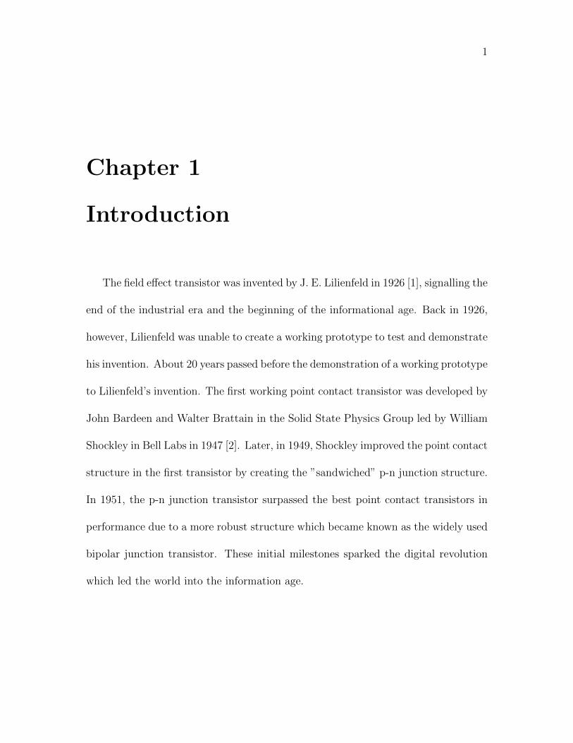
The field effect transistor was invented by J. E. Lilienfeld in 1926 [1], signalling the
end of the industrial era and the beginning of the informational age. Back in 1926,
however, Lilienfeld was unable to create a working prototype to test and demonstrate
his invention. About 20 years passed before the demonstration of a working prototype
to Lilienfeld’s invention. The first working point contact transistor was developed by
John Bardeen and Walter Brattain in the Solid State Physics Group led by William
Shockley in Bell Labs in 1947 [2]. Later, in 1949, Shockley improved the point contact
structure in the first transistor by creating the ”sandwiched” p-n junction structure.
In 1951, the p-n junction transistor surpassed the best point contact transistors in
performance due to a more robust structure which became known as the widely used
bipolar junction transistor. These initial milestones sparked the digital revolution
which led the world into the information age.
2
(a) (b)
Figure 1.1: The first transistors. The demonstration of the (a) first point contacttransistor by J. Bardeen, W. Brattain, and W. Shockley (Bell Laboratories 1947),and (b) the first transistor with diffused P-N junctions by William Shockley (BellLaboratories 1949).
The digital revolution triggered a chain of exponentially faster technological ad-
vancements, dramatically changing the worldwide economy, science, and communi-
cations. In 1955, Shockley left Bell Labs to form Shockley Semiconductors, the origin
of Silicon Valley. Later, in 1957, a group of researchers, including Gordon Moore,
resigned from their jobs at Shockley Semiconductors because Shockley decided to
no longer continue research into silicon-based semiconductors. These researchers
formed the first successful semiconductor company, Fairchild Semiconductor. One of
the milestones attributed to their work at Fairchild Semiconductor was the introduc-
tion of the planar process for fabricating transistors that is still used today more than
a half century later [3]. Although the first integrated circuit (IC) was developed by
3
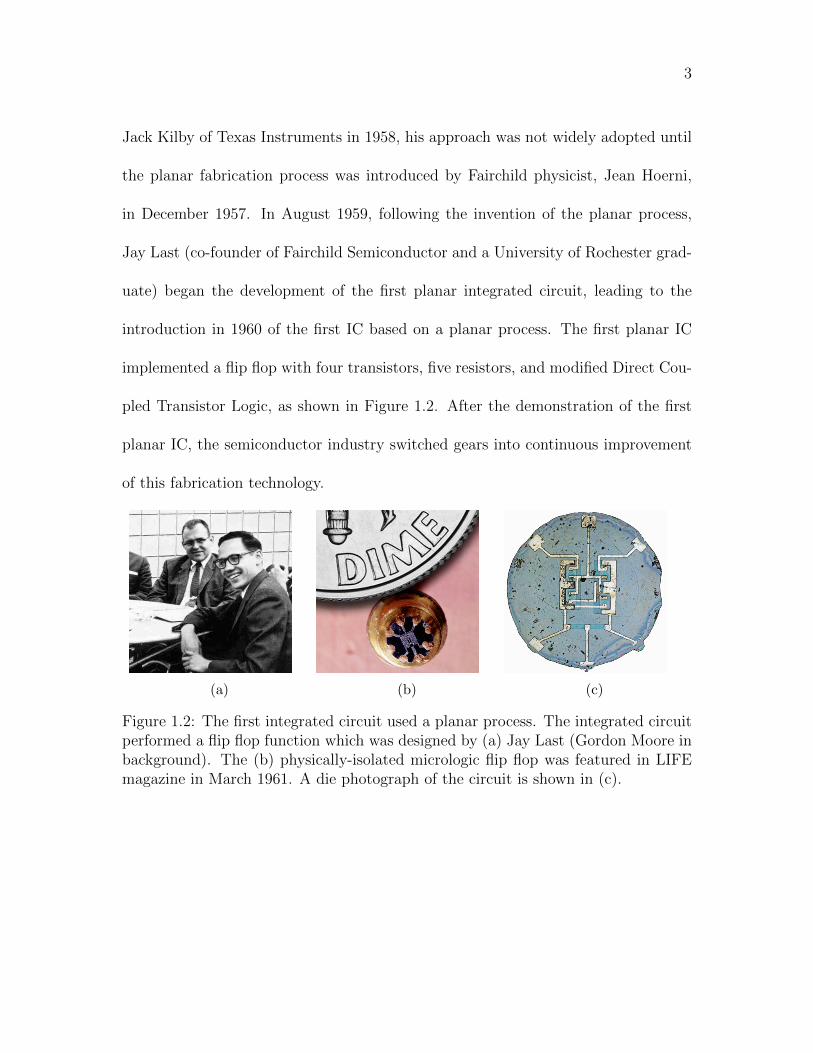
Jack Kilby of Texas Instruments in 1958, his approach was not widely adopted until
the planar fabrication process was introduced by Fairchild physicist, Jean Hoerni,
in December 1957. In August 1959, following the invention of the planar process,
Jay Last (co-founder of Fairchild Semiconductor and a University of Rochester grad-
uate) began the development of the first planar integrated circuit, leading to the
introduction in 1960 of the first IC based on a planar process. The first planar IC
implemented a flip flop with four transistors, five resistors, and modified Direct Cou-
pled Transistor Logic, as shown in Figure 1.2. After the demonstration of the first
planar IC, the semiconductor industry switched gears into continuous improvement
of this fabrication technology.
(a) (b) (c)
Figure 1.2: The first integrated circuit used a planar process. The integrated circuitperformed a flip flop function which was designed by (a) Jay Last (Gordon Moore inbackground). The (b) physically-isolated micrologic flip flop was featured in LIFEmagazine in March 1961. A die photograph of the circuit is shown in (c).
4
The semiconductor industry has since been faced by a fundamental tradeoff among
speed, power, and area. Increasing the speed of an IC leads to higher power con-
sumption. Alternatively, reducing power consumption lowers the speed or increases
the area of the circuit, as discussed in Chapter 2. One technique, however, enables
simultaneous improvements in all the three primary design criteria of the semicon-
ductor industry, area, speed, and power. This technique, miniaturizing the device
and interconnect feature size (or scaling), has become the primary driver of tech-
nological improvement in integrated circuits. Smaller feature sizes improve density,
simultaneously providing more transistors and functionality. With a shorter transis-
tor channel, the supply voltage can also be scaled, lowering the power consumption.
1
10
100
1,000
10,000
100,000
1,000,000
10,000,000
1965 1970 1975 1980 1985 1990 1995 2000 2005 2010 2015 2020
Num
bero
ftransistors(T
housan
ds)
Haswell
IvyBridge
SandyBridge
Pen<um4
Pen<um
286
4004
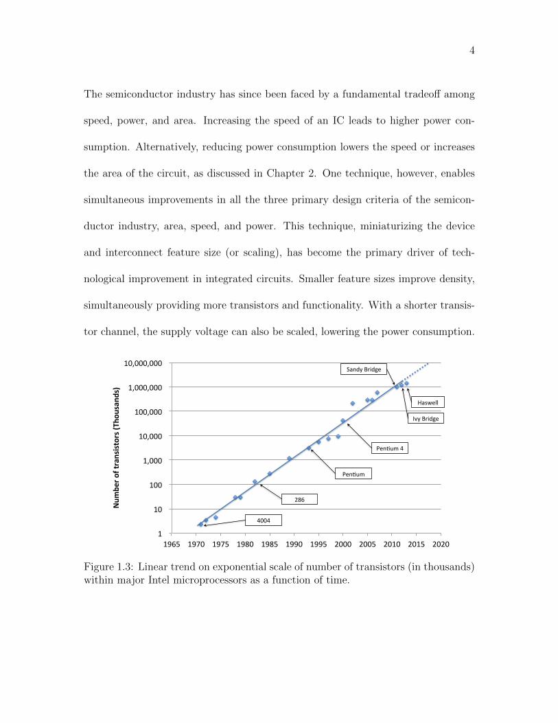
Figure 1.3: Linear trend on exponential scale of number of transistors (in thousands)within major Intel microprocessors as a function of time.

5
The thinner gate oxide produces a lower threshold voltage, speeding up the tran-
sistor. Scaling the transistor has been embraced by the semiconductor industry, as
illustrated in Figure 1.3.
1.1 Low power circuits and techniques
The annual doubling of transistor count and the performance benefits of scaling
fueled the megahertz race in the beginning of the 21st century. During that time,
AMD and Intel went head to head to release a higher clock frequency microprocessor
since the costumers were convinced that higher clock speeds equated to better mi-
croprocessor performance. This race however came to an end in the mid 2000’s when
Intel produced the Pentium 4 microprocessor with power densities that approach
the power density of a nuclear reactor [4]. Realizing that current design techniques
that prioritize frequency stumbled upon the power density wall, Intel switched to
more power efficient processors while AMD lagged. These processors were the Core
series, the successors of the successful low power notebook microprocessor, Pentium
M (codenamed Banias) was developed in the Intel Development Center in Israel in
2003. Lower power consumption increased the core count while operating at power
consumption levels within a single core Pentium 4 processor power envelope. The
power density wall is illustrated in Figure 1.4 where the number of transistors grows
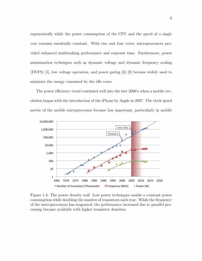
6
exponentially while the power consumption of the CPU and the speed of a single
core remains essentially constant. With two and four cores, microprocessors pro-
vided enhanced multitasking performance and response time. Furthermore, power
minimization techniques such as dynamic voltage and dynamic frequency scaling
(DVFS) [5], low voltage operation, and power gating [6]–[8] became widely used to
minimize the energy consumed by the idle cores.
The power efficiency trend continued well into the late 2000’s when a mobile rev-
olution began with the introduction of the iPhone by Apple in 2007. The clock speed
metric of the mobile microprocessor became less important, particularly in mobile
1
10
100
1,000
10,000
100,000
1,000,000
10,000,000
1965 1970 1975 1980 1985 1990 1995 2000 2005 2010 2015 2020
Numberoftransistors(Thousands) Frequency(MHz) Power(W)
PenGum4
Core2Duo
Figure 1.4: The power density wall. Low power techniques enable a constant powerconsumption while doubling the number of transistors each year. While the frequencyof the microprocessors has stagnated, the performance increased due to parallel pro-cessing became available with higher transistor densities.
7
applications. The central processing unit (CPU) evolved into many small, power
efficient, and dedicated cores, all integrated within a single die. Unconstrained by
general functionality, these dedicated cores could be improved when active to deliver
significantly better speed and power efficiency. Alternatively, when not needed, these
cores are power gated to save stand-by power. These technological advancements
coupled with the widespread use of mobile devices and mobile phones reinforced the
need for power efficient circuits. The increased demand for mobility and battery
efficiency provided a fertile ground and the financial investment needed to develop
advanced low power circuits.
Research in low power techniques has reignited interest in near and subthreshold
circuits (for low voltage operation). From the perspective of energy efficiency, sub-
threshold circuits exhibit the lowest energy operating characteristics. The increased
energy efficiency, however, comes with a significant penalty in circuit speed. An al-
ternative technique that provides significant energy efficiency with less of a dramatic
slow down in speed are near threshold circuits (NTC). Both of these techniques, as
discussed in Section 2, are in the early stages of development and are not as yet
widely adopted by industry.

8
1.2 Outline
Developing energy efficient systems without a significant sacrifice in performance
is a primary issue in modern sub-30 nm CMOS microprocessors [9]. A review of
the major power dissipation components of high complexity CMOS-based integrated
circuits is provided in Chapter 2. In this chapter, the dynamic, short-circuit, and
leakage power are individually described. Standard power reduction techniques for
each power component are also reviewed.
Techniques such as dynamic voltage scaling operating down to near threshold
voltage levels while supporting multiple voltage domains are commonly used to re-
duce both dynamic and static power. A key component of these techniques is a level
shifter which supports different voltage domains. To reduce the system overhead, this
level shifter needs to exhibit both high speed and power efficiency. A circuit that
translates voltages ranging from 250 mV to 790 mV while exhibiting 42% shorter
delay, 45% lower energy consumption, and 48% lower static power dissipation as
compared to published circuits is described in Chapter 3.
Although a level shifter enables operation at low voltages, a primary issue that
limits dynamic frequency and voltage scaling is the inability to optimize interconnect
to support a wide voltage range from nominal to subthreshold voltages. To address
this issue, a closed-form delay model supporting wide voltage ranges is described

9
in Chapter 4. This model supports an ultra-wide voltage ranging from nominal
voltages to deep subthreshold voltages. The model exhibits good accuracy across
the entire parameter space with the worst case error from 9% to -17% (17% to -17%
in the subthreshold region) for long interconnect lines with repeaters. Challenges to
repeater insertion are also discussed based on the proposed model.
Near threshold circuits are an attractive and promising technology that provides
significant power savings with some delay penalty. A novel approach of combining
near threshold circuit technology with MOS current mode logic (MCML) is exam-
ined in Chapter 5. By combining MCML with near threshold circuits, the constant
power consumption of MCML is reduced to leakage power levels. Additionally, the
speed of near threshold circuits is improved due to the high speed nature of MCML.
This technique has been developed to minimize the speed penalty in power efficient
microprocessors.
Static power consumes a significant portion of the available power budget in
modern sub-30 nm CMOS microprocessors. Consequently, leakage current reduction
techniques such as power gating have become necessary. The standard power gating
approach provides static power savings during times when the power gated circuit is
idle. This approach introduces a speed penalty during the active times of the circuit,
as well as a significant latency entering and leaving the sleep mode. These delay

10
overheads, therefore, limit the application of standard power gating to low activity
circuits. To overcome these limitations, an adaptive power gating technique has been
developed, as discussed in Chapter 6. This high granularity adaptive power gating
approach employs a local controller to selectively power gate the inactive portions of
a circuit. This method enables additional power savings when a power gated circuit
is partially active without halting circuit operation, as opposed to standard power
gating approaches [8].
The dissertation is concluded with directions for future research in Chapter 8 and
a summary in Chapter 7.
11
Chapter 2
Power consumption and reductiontechniques in CMOS circuits
In the era of handheld mobile devices, the power consumption of an integrated
circuit is a primary concern [9]. The total power consumed by a circuit consists of
three major parts, as given by
Ptotal = Pdynamic + Pshort circuit + Pleakage. (2.1)
The first term in (2.1), the dynamic power component, is due to charging/discharging
the parasitic and output capacitances in response to changes in the input of the
circuit. The second component is the short-circuit power, the power consumed during
a transition when both of the NMOS and PMOS transistors in a logic gate are
simultaneously on. The leakage power is the third term of the total power, and
consists of undesirable currents passing through the gate, diffusions, and channel of

12
the transistors when the circuit is idle.
Historically, the leakage and short-circuit terms of the total power dissipation
have been neglected by assuming a well designed integrated circuit. In these circuits,
the leakage and short-circuit power components are insignificant. More recently, the
leakage current has become significant. In some cases, the dynamic power consump-
tion is no longer the major source of power dissipation as the leakage power has
become comparable or greater. Alternatively, the short-circuit power is still some-
what insignificant in a well designed circuit (approximately 10% to 20% of the total
power).
The dynamic, short-circuit, and leakage power components of the total power
consumption are characterized in the rest of the chapter. Dynamic power and power
reduction techniques are described in Section 2.1. Short-circuit power is discussed in
Section 2.2. The significance of leakage power and leakage reduction techniques are
discussed in Section 2.3.
2.1 Dynamic power component
During switching of a circuit, the majority of the power is dissipated by charg-
ing the parasitic and load capacitances, and converted to heat through the parasitic
resistances. When the output of a gate, e.g., an inverter, switches from 0 to 1, the
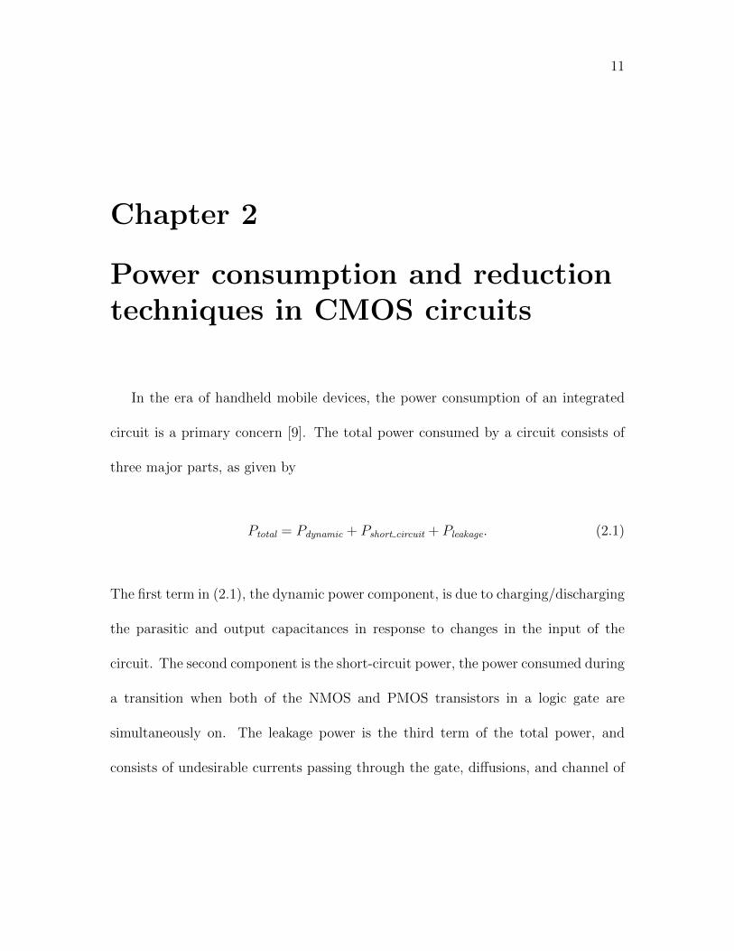
13
output capacitor CL charges to the high supply voltage VDD through the PMOS
pull-up transistor. This low-to-high transition at the output consumes CLV2DD en-
ergy. Half of the energy is lost across the parasitic resistance of the PMOS pull-up
transistor and dissipated as heat, and the other half is stored in the output capacitor.
Later, during the high-to-low transition, the stored half of the consumed dynamic
energy (12CLV
2DD) is discharged to ground through the NMOS pull-down transistor,
as shown in Figure 2.1. In the worst case, this process repeats every clock period
Vin
VDD
VSS
Vout
CL
E1 =12CLVDD
2
(a)
Vin
VDD
VSS
Vout
CLE2 =
12CLVDD
2
(b)
Figure 2.1: Dynamic energy consumption in a standard CMOS inverter. Half of theconsumed energy is dissipated across the parasitic capacitance of the PMOS transis-tor during the a) rise transition, and the other half is stored in the output capacitorCout. This stored energy is discharged to ground during the b) fall transition.
T = 1/f , resulting in dynamic power dissipation equal to CLV2DDf . Practically,
however, general logic switches less frequently with a transition probability α which
is also referred to as the activity factor of a circuit. These factors are described by
14
the dynamic power in the classical expression,
Pdynamic = αCLV2DDf, (2.2)
where α is the switching activity factor of the circuit, CL is the output capacitance
being charged/discharged, VDD is the supplied voltage, and f is the operating fre-
quency of the circuit. Reducing the value of any variable in the equation results in
lower dynamic power consumption. Special attention however should be given to
reducing the transition voltage due to the quadratic effect on the dynamic power.
After the reduction in voltage is exhausted, the next step is to minimize the effec-
tive capacitance Ceffective which includes the transition activity factor as given by
Ceffective = αCL. A reduction of the effective capacitance generally requires high level
optimization such as the choice of logic function, logic style, circuit topology, input
data statistics, and sequence of operations. The frequency of the circuit can also be
reduced to lower the power dissipation. Decreasing the frequency is undesirable since
the operating frequency is less. Additionally, a low operating frequency increases the
idle time of the circuit, which increases the relative significance of the leakage power
component of the total power consumption. With a lower frequency, the leakage
power component can overshadow the dynamic power, as discussed in Section 2.1.1.
15
Nevertheless, there are low power techniques that efficiently employ frequency reduc-
tion. Dynamic frequency scaling (DFS) reduces the frequency to efficiently reduce
the power consumed by the clock buffers, latches, and logic [7]. When a circuit is
moderately active or a fast system response is not required, the frequency is dynam-
ically reduced to lower the dynamic power of the circuit and clock infrastructure.
Additionally, for idle circuits, an active clock is not required, saving which wastes
power. In such a case, the switching activity of the clock is stopped to conserve the
power dissipated by the clock distribution network.
2.1.1 Subthreshold circuits
As described in Section 2.1, the dynamic power is proportional to V 2DD. A
quadratic improvement in dynamic power consumption is therefore achieved by lin-
early decreasing the supply voltage. This approach is constrained by how low the
voltage can be reduced while simultaneously decreasing power. In 1972, Meindl et
al. described a theoretical lower limit of VDD for logic operation equal to 8kT/q or
approximately 200 mV at room temperature [10]. There has since been significant in-
terest in subthreshold circuit operation, initially for analog circuits and more recently
for digital processors [11], where operation has been experimentally demonstrated at
VDD = 280 mV.
16
This dramatic reduction in dynamic power consumption is unfortunately coupled
with a significant penalty in speed. The exact expression for circuit delay that
considers the nonlinear characteristics of a CMOS gate is quite complex; therefore, a
simple expression is used to predict the experimentally determined dependence [12].
The delay of a CMOS gate is approximated by
TD =1
f=CLVDDIsat
=CLVDD
µCox
2(W/L)(VDD − Vth)2
. (2.3)
From this delay equation, it can be shown that circuit speed is proportional to
(VDD−Vth)2VDD
. This relation, however, is less accurate as VDD is reduced to near and
below the threshold voltage of the transistor. At these low supply voltages, the
current sourced by a transistor is exponentially dependent upon the supply voltage
[13],
Isub ∝ e(VDD−Vth). (2.4)
Below the threshold voltage, therefore, the speed degrades exponentially with supply
voltage. When considering the entire operating voltage range, it is more convenient to
examine the energy per operation (power-delay product), eliminating the dependence
17
on speed. The energy consumption per operation is
Eper operation = Pdynamic × TD = Pdynamic ×1
f. (2.5)
Substituting (2.2) into (2.5), the speed independent relationship for energy is
Eper operation ∝ V 2DD. (2.6)
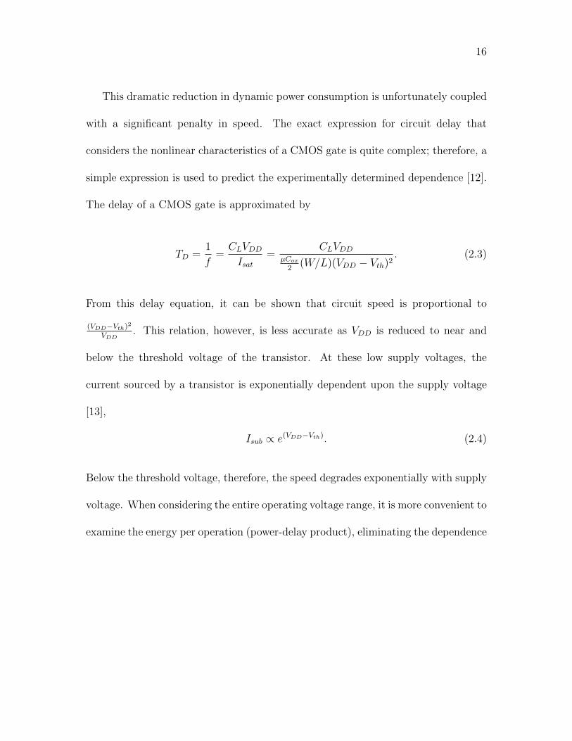
This discussion is illustrated in Figure 2.2 where the energy per operation and circuit
speed are shown as a function of supply voltage. In this figure, the dramatic reduction
in energy consumption from the super threshold region to the subthrehold region of
operation is noted. This dramatic reduction in energy is coupled with a significant
drop in circuit speed.
More importantly, however, the minimum energy operating point is located within
the subthreshold region. If the supply voltage is reduced below this operating point,
the circuit becomes less power efficient due to the increasing dominance of leakage
power over dynamic power. The speed of the circuit below this operating point
is extremely slow, about three orders of magnitude slower than nominal. At these
speeds, the circuit leaks power without producing a significant computational output.
However, if the operating point of the circuit is maintained near the minimum energy
18
Ene
rgy/
Ope
ratio
n Sub-Vth region Super-Vth region
Supply Voltage Vth Vnominal
~20x
(a)
Log
(Fre
quen
cy)
Supply Voltage Vth Vnominal
~500 - 1,000x
(b)
Figure 2.2: Performance of a CMOS circuit within two regions of operation. Thesubthreshold region includes supply voltages below Vth, and nominal operating regionis represented by voltages above Vth. The graphs show a) energy per operation, andb) speed as a function of supply voltage.
point by dynamically sensing and adjusting the circuit parameters, and if the speed
of the circuit does not represent a mandatory constraint, the subthreshold region of
operation provides the most energy efficient operation. For example, circuits such as
biological sensors, cardiac pacemakers, satellites, and energy harvesting applications
require extremely low energy consumption without a significant requirement for high
speed, and are therefore well suited to operate within subthreshold region.
The speed penalty, however, is not the only tradeoff in utilizing the low voltage
19
region of operation. Additional supporting circuits are required, such as a voltage
level shifter to translate low voltage signals from the subthreshold logic to above
threshold voltage domains (and vice versa). These additional circuits and other
tradeoffs of low voltage operation are described in Section 2.1.2.
2.1.2 Near threshold circuits
Another approach to reduce power consumption by lowering the supply voltage
is the use of near threshold circuits (NTC) technique. This technique differs from
earlier subthreshold circuit approaches in that the supply voltage is not drastically
reduced to the minimum energy consumption level. Rather, in this technique, the
supply voltage is lowered to near the threshold voltage of the transistors. This less
extreme approach allows near threshold circuits to consume an order of magnitude
lower power than circuits operating under nominal voltages while not suffering from
the significant delay penalty in deep subthreshold circuits. NTC has therefore become
an attractive methodology for sub-30 nm low power CMOS circuits [11]. By oper-
ating near the threshold voltage (as compared to a much lower voltage deep within
the subthreshold region), near threshold circuits represent a balanced approach to
tackling the power issue while maintaining circuit delays within a reasonable range.
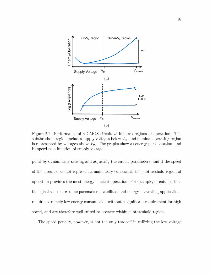
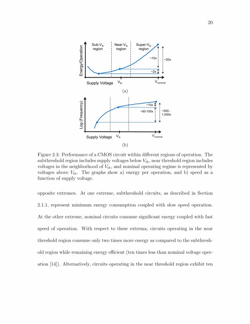
This concept is illustrated in Figure 2.3. In this figure, NTC is compared to two
20
Ene
rgy/
Ope
ratio
n Sub-Vth region
Near-Vth region
Super-Vth region
~2x
~10x
Supply Voltage Vth Vnominal
~20x
(a)
Log
(Fre
quen
cy)
~50-100x
~10x
Supply Voltage Vth Vnominal
~500 - 1,000x
(b)
Figure 2.3: Performance of a CMOS circuit within different regions of operation. Thesubthreshold region includes supply voltages below Vth, near threshold region includesvoltages in the neighborhood of Vth, and nominal operating regime is represented byvoltages above Vth. The graphs show a) energy per operation, and b) speed as afunction of supply voltage.
opposite extremes. At one extreme, subthreshold circuits, as described in Section
2.1.1, represent minimum energy consumption coupled with slow speed operation.
At the other extreme, nominal circuits consume significant energy coupled with fast
speed of operation. With respect to these extrema, circuits operating in the near
threshold region consume only two times more energy as compared to the subthresh-
old region while remaining energy efficient (ten times less than nominal voltage oper-
ation [14]). Alternatively, circuits operating in the near threshold region exhibit ten
21
times longer delays as compared to circuits operating in the nominal voltage region.
The delay of circuits operating in the subthreshold region can be a hundred to a
thousand times greater than NTC [14].
One of the difficulties of operating near the threshold voltage is the increased
sensitivity to process, voltage, and temperature variations (PVT). Small variations in
supply voltage can greatly affect the operating point (speed and power consumption)
of NTC. Power noise in the range of 50 to 100 mV can shift the operating point from
above the threshold voltage to below the threshold voltage, essentially pushing NTC
either to subthreshold or above threshold operation. Alternatively, the threshold
voltage can shift due to process variations, leading to the same effect, placing a circuit
either in the subthreshold region or above the threshold voltage. This behavior can
lead to large shifts in gate drive capabilities of NTC transistors due to the exponential
dependence of gate current on supply and threshold voltages [15]. Additionally, the
low power characteristics of NTC degrade when the supply voltage is above the
threshold voltage.
Another difficulty with near threshold circuits is that several parts of a micropro-
cessor require nominal voltages to maintain correct operation. A six transistor cell
SRAM, for example, cannot reliably operate at voltages much lower than the full
supply voltage [16]. These high voltage memory cells combined with near threshold
22
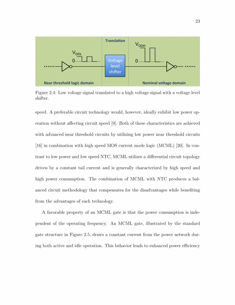
logic are often integrated into the same multi-voltage domain microprocessor [17],
[18]. For example, in the case of a low voltage signal originating from near threshold
logic, the signal needs to be correctly stored within the memory and propagated
through the high voltage memory domain. If these two voltage domains are directly
connected, the low voltage input signal will not entirely switch off the high voltage
PMOS network at the boundary of the high voltage memory domain, allowing short-
circuit current to flow between the power supply and ground. This effect leads to
two undesirable problems, excessive power consumption and potential corruption of
the output signal which can result in system failure. Voltage level shifters, there-
fore, play an important role in heterogeneous systems. In these environments, level
shifters allow a signal to propagate between different voltage domains, as illustrated
in Figure 2.4. To reduce the overhead, these multi-voltage systems require an effi-
cient level shifter that converts the voltage between the multi-voltage domains [19].
A discussion of different level shifters that can operate over a wide voltage range is
the focus of Chapter 3.
2.1.3 Advanced near threshold circuits
As described in previous sections, near threshold circuits represent a balanced
approach to minimizing power consumption with a reasonable degradation in circuit
23
Nominal voltage domain Near threshold logic domain
VDDL
0
Transla3on
Voltage level shi-er
VDDH
0
Figure 2.4: Low voltage signal translated to a high voltage signal with a voltage levelshifter.
speed. A preferable circuit technology would, however, ideally exhibit low power op-
eration without affecting circuit speed [9]. Both of these characteristics are achieved
with advanced near threshold circuits by utilizing low power near threshold circuits
[16] in combination with high speed MOS current mode logic (MCML) [20]. In con-
trast to low power and low speed NTC, MCML utilizes a differential circuit topology
driven by a constant tail current and is generally characterized by high speed and
high power consumption. The combination of MCML with NTC produces a bal-
anced circuit methodology that compensates for the disadvantages while benefiting
from the advantages of each technology.
A favorable property of an MCML gate is that the power consumption is inde-
pendent of the operating frequency. An MCML gate, illustrated by the standard
gate structure in Figure 2.5, draws a constant current from the power network dur-
ing both active and idle operation. This behavior leads to enhanced power efficiency
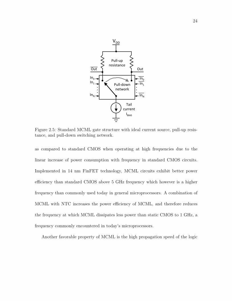
24
In0
In1
InN
Out
In0 In1
InN
Out
Tail current IBIAS
Pull-‐down network
Pull-‐up resistance
VDD
Figure 2.5: Standard MCML gate structure with ideal current source, pull-up resis-tance, and pull-down switching network.
as compared to standard CMOS when operating at high frequencies due to the
linear increase of power consumption with frequency in standard CMOS circuits.
Implemented in 14 nm FinFET technology, MCML circuits exhibit better power
efficiency than standard CMOS above 5 GHz frequency which however is a higher
frequency than commonly used today in general microprocessors. A combination of
MCML with NTC increases the power efficiency of MCML, and therefore reduces
the frequency at which MCML dissipates less power than static CMOS to 1 GHz, a
frequency commonly encountered in today’s microprocessors.
Another favorable property of MCML is the high propagation speed of the logic
25
gates. MOS current mode logic operates at frequencies significantly higher than
standard CMOS. These frequencies are achieved due to the low delay of MCML,
which is largely due to the reduced voltage swing of MCML gates. The voltage
swing of an MCML gate is typically two to ten times lower than VDD.
Finally, MCML logic benefits from a low noise environment. The constant switch-
ing activity of CMOS circuits results in simultaneous switching noise (SSN) which
is a significant source of on-chip noise [21]. In contrast, the near constant current of
MCML (regardless of the state, i.e., idle, transition, active) produces significantly less
on-chip SSN. The low noise of MCML is particularly relevant when combined with
NTC due to the exponential sensitivity of NTC circuits to supply voltage variations
[14]. A noise analysis of these circuits is described in Section 5.4.2.
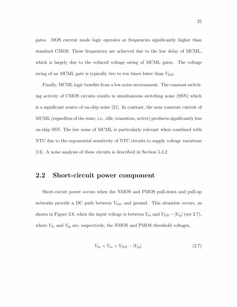
2.2 Short-circuit power component
Short-circuit power occurs when the NMOS and PMOS pull-down and pull-up
networks provide a DC path between VDD and ground. This situation occurs, as
shown in Figure 2.6, when the input voltage is between Vtn and VDD−|Vtp| (see 2.7),
where Vtn and Vtp are, respectively, the NMOS and PMOS threshold voltages,
Vtn < Vin < VDD − |Vtp|. (2.7)
26
Vin
t
VH
VL
VDD
VSS
ISC VinVout
VoutIshort
circuit
Slow transition
VH-|Vtp|
Vtn
Figure 2.6: Short-circuit current sourced by partially closed PMOS and sunk bypartially open NMOS in a CMOS inverter gate.
In more poorly designed circuits, the input and output transitions are long and
asymmetric. The condition described by (2.7) will therefore exist for longer times,
allowing greater power losses due to undesired short-circuit current. To lower this
parasitic current, it is desirable to have sharp and equal input and output transition
times. By sizing the gate transistors for equal rise and fall times, the short-circuit
component of the total power dissipation can be less than 5% to 10% of the dynamic
switching component [22].
27
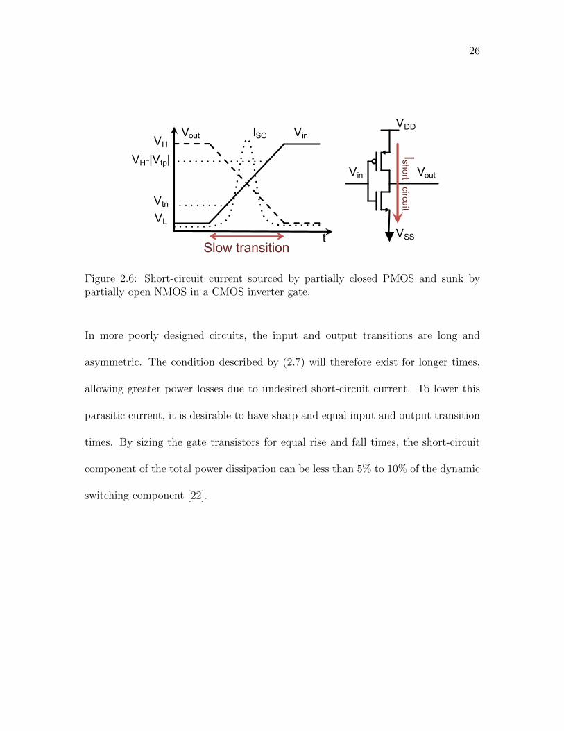
2.3 Leakage power component
Leakage power occurs from a number of different leakage current paths. The
major contributors are reverse-bias diode leakage current through the transistor dif-
fusions, the subthreshold current through the channel of an off device, and, to a
smaller degree, gate tunneling current, as shown in Figure 2.7. The reverse-bias
diode leakage current occurs when a transistor is turned off and another active de-
vice charges the drain with respect to the bulk of the off device. Consider an inverter
with a high input voltage where the NMOS transistor is turned on and the output
voltage is driven low. The resulting leakage current through the drain of the PMOS
Gate leakag
e
Vin
VDD
VSS
Vout
Subthreshold leakage
(a)
Gate
Drain Source 1 2 3
4 5
4
(b)
Figure 2.7: Leakage current paths in a) standard CMOS gate, and b) MOS transistor.The MOS transistor provides gate-to-drain (1) and gate-to-source (2), subthreshold(3), drain-to-substrate (4), source-to-substrate (4), and channel-to-substrate (5) leak-age currents currents.
transistor is approximately Idiode = AD × JS where AD is the area of the drain diffu-
sion, and JS is the leakage current density, set by technology and weakly dependent
28
on the supply voltage. The subthreshold current through an off transistor is due
to carrier diffusion between the source and drain when the gate-to-source voltage
VGS exceeds the weak inversion point but is below the threshold voltage Vth. In this
regime, carrier drift is the dominant current source and depends exponentially on
the gate-to-source voltage VGS. The current in the subthreshold region is
IDS = ke(VGS−Vth)/(nVT )(1− eVDS/VT ), (2.8)
where k is a technology constant, VT is the thermal voltage equal to KT/q, and Vth
is the threshold voltage.
In recent years due to aggressive scaling of the minimum feature size to enhance
speed, area, and power, the threshold voltage, channel length, and gate oxide thick-
ness have been significantly reduced. A nanometer scale gate oxide leaves insufficient
material to prevent oxide tunneling. Additionally, the deeply scaled channel increases
the source-to-drain leakage current. These factors contribute to the significant in-
crease in leakage current above previously accepted levels, revealing a weakness in
deeply scaled transistors. This issue has resulted in a push toward enhanced transis-
tor structures. A high-K dielectric was introduced by Intel to reduce gate tunneling
leakage current [23]. An advanced 3-D transistor topology with FinFET transistors
was later introduced to improve gate control and full depletion of the channel [24].

29
The FinFET transistor has a channel in a form of a fin with a gate wrapped around
the fin to increase the gate area and reduce the channel depth, providing a fully
depleted channel.
Nevertheless, despite these latest advancements in transistor technology, gate
and channel leakage current is increasing to the point where the dynamic power
consumption of the modern circuits is not the major component of power dissipation
[25]. Circuit techniques to lower leakage power, therefore, have become a primary
objective in modern microprocessors [9]. One of the more efficient techniques to
manage leakage current is power gating, which is described in Section 2.3.1.
2.3.1 Power gating
Power gating is a well known and efficient technique to reduce leakage current [8].
The principle of power gating is to disconnect a circuit from the power supply network
by a power switch when the circuit is inactive. This method requires integrating
additional circuit components within the power gated circuit. Additional power
switches are inserted between the power distribution network and the logic. Isolation
cells are placed at the boundaries of the power gated circuit to disconnect floating
outputs from the powered down logic. State retention registers are required in case
the logic state is required for further operation after wakeup of the circuit. Finally,
30
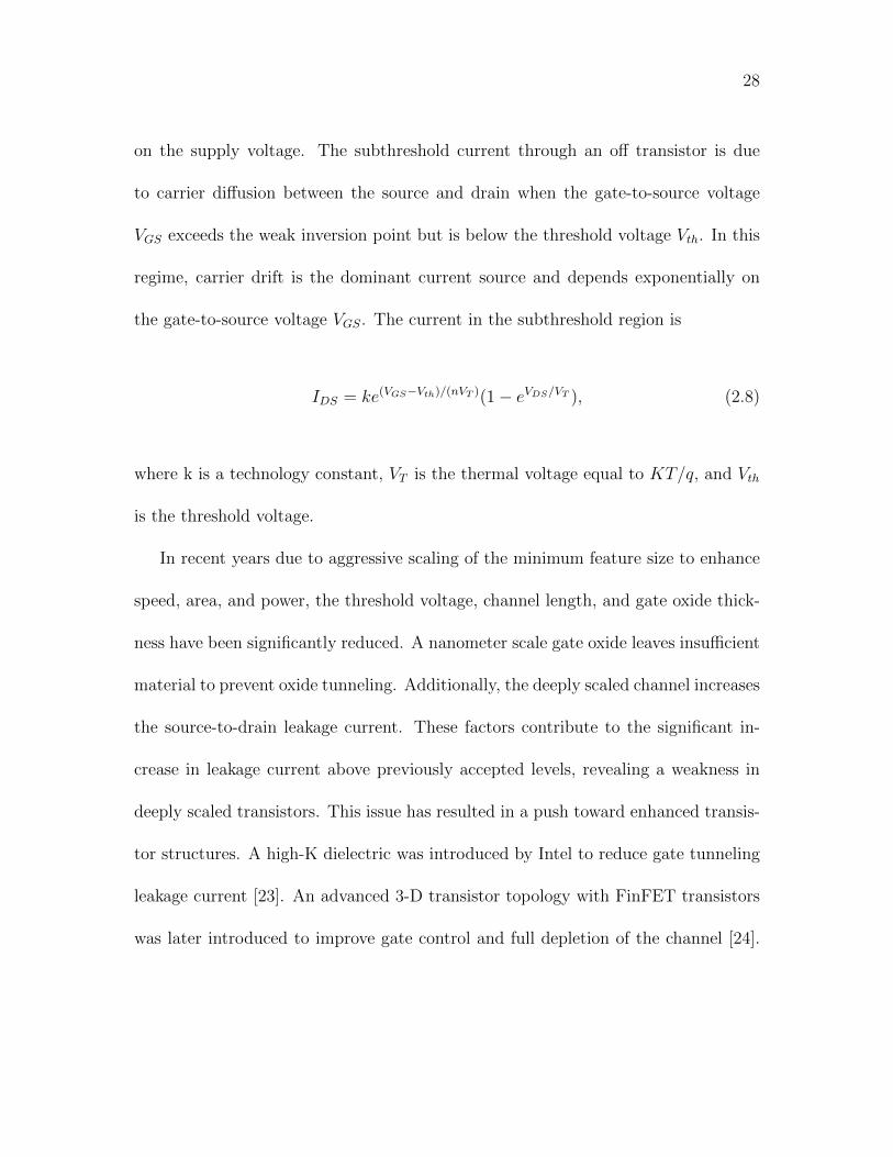
a controller oversees and synchronizes the operation of these additional blocks, as
illustrated in Figure 2.8.
Activeblock
VSS
Isolation
Power gating controller
VDD
Powergatedblock
StateRetention
CLK
CLKGate
Power switches
Figure 2.8: Components of power gating system
A number of power gating approaches has been evaluated in the literature ranging
from coarse grain versus fine grain and global versus local power gating. Microprocessor-
wide global power gating has significant overhead such as sleep and wake up delay,
layout congestion, and area overhead. Due to the large number of transistors that are
power gated and the occasional need to save the logic state, the sleep and wake up
delay is significantly long, and can require a number of clock periods. Additionally,
global control lines need to be routed to the power gated circuit, increasing layout
congestion. These overheads as well as the complexity of system-wide integration
31
have limited industry wide adoption of global power gating [26]. Alternatively, a
local power gating technique is employed often to alleviate the overhead of global
power gating. These local techniques employ a local controller in close proximity to
the gated circuit which enables fine grain power gating by adapting to the current
state of a clustered circuit. The local and adaptive controller reduces the need for
global control lines as well as lowers system complexity. Additionally, the local power
gating approach improves the response time and enables higher energy savings, as
discussed in Chapter 6.
2.4 Summary
Power consumption and reduction techniques in CMOS circuits are discussed in
this chapter. Power consumption in integrated circuits is a major concern in deeply
scaled technologies. The recent revolution of portable battery powered devices has
raised the demand for highly power efficient microprocessors and systems-on-chip.
In parallel, the relative significance of leakage power over dynamic power has been
increasing due to transistor scaling.
Power reduction techniques are employed to address these two primary concerns
by reducing the dynamic power and leakage power components of the total power

32
consumption. These components are major contributors to the total power dissi-
pated in standard CMOS circuits. The dynamic power component exhibits a linear
dependence on the effective capacitance and frequency, and a quadratic dependence
on the supply voltage. Low power techniques that reduce dynamic power, therefore,
focus on lowering the supply voltage to quadratically reduce power consumption.
These techniques include subthreshold circuits that enable maximum energy effi-
ciency. Subthreshold circuits, however, exhibit a significant two to three orders of
magnitude speed penalty. The high delay of this technique limits applications to
those circuits that demand low power consumption while not constrained by slow
operating speed. For general purpose circuits, a high delay is not practical and a
more balanced approach is used. Near threshold circuits target circuits that can
compromise some speed reduction for significantly higher power efficiency. When
the circuit operates near the threshold voltage, the speed penalty is only 10% to 20%
of the delay of subthreshold circuits. However, up to 80% of the energy of subthresh-
old circuits is maintained. Additionally, advanced techniques are reviewed in this
chapter, such as MOS current mode logic operating near the threshold voltage to
further improve power efficiency without significantly compromising circuit speed.
With this combination of MCML and NTC, high activity circuits can operate at
higher energy efficiency above 1 GHz as compared to standard CMOS NTC.

33
Alternatively, leakage power is addressed primarily by reducing idle times, or by
disconnecting the power supply network from the inactive logic. Power gating is
a well studied approach to reduce leakage power by disconnecting the circuit from
the power supply. This technique is based on power switches, which are PMOS or
NMOS transistors inserted between the power network and the power gated circuit.
Although power gating is not a new approach, it has gained popularity only recently
since the savings in leakage power has surpassed the rather high power overhead
of the technique. The cost of applying global power gating is high due to routing
congestion and area overhead as well as the additional supporting circuits that control
the shut down and wake up processes and maintain a correct logic state during
transitions. Local power gating, however, reduces routing congestion and response
time by utilizing a local and autonomous controller.
34
Chapter 3
Power efficient level shifter for 16nm FinFET near threshold circuits
Scaling of the supply voltage is a widely used method to reduce power con-
sumption in modern microprocessors. When the supply voltage approaches near the
threshold voltage of the transistor, an optimal energy efficiency is enabled by balanc-
ing the speed and power consumption of a circuit. Several parts of a microprocessor,
however, need to operate at nominal voltages. A 6T SRAM, for example, cannot
reliably operate at voltages much lower than the full supply voltage [16]. These
high voltage memory cells combined with near threshold logic are often integrated
into the same multi-voltage domain microprocessor [17], [18]. The integration of
multi-supply voltage circuits within the same microprocessor requires an efficient
level shifter that converts the voltage between the multi-voltage domains [19]. A
novel power efficient level shifter topology operating over a wide voltage range is the

35
focus of this chapter. The circuit supports voltages ranging from a low subthreshold
voltage (approximately 250 mV) to a high voltage domain (for example, 790 mV).
The chapter is structured as follows. The operation of existing standard and
advanced level shifter circuits is reviewed in Section 3.1. The proposed wide voltage
range level shifter circuit is described in Section 3.2. The simulation environment
and results are provided, respectively, in Sections 3.3.1 and 3.3.2. The chapter is
summarized in Section 3.4.
3.1 Previous work
Level shifter circuits are typically based on one of three approaches. One approach
is based on a DCVS level shifter. This approach is discussed in this section to
exemplify the basic principles used by the proposed level shifter. A second approach
uses a wilson current mirror in the amplifying stage [27], [28]. The third approach
utilizes a specialized circuit topology [19].
3.1.1 Standard level shifter
A standard level shifter topology is typically based on a differential cascade volt-
age switch (DCVS) gate [29]–[32]. A DCVS level shifter circuit is illustrated in Figure
3.1.
36
Low voltage input
High supply voltage
out out
in in NL NR
PL PR
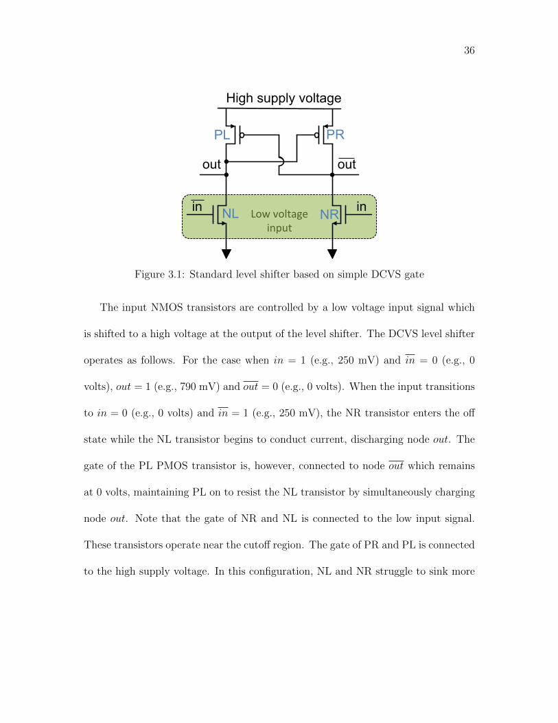
Figure 3.1: Standard level shifter based on simple DCVS gate
The input NMOS transistors are controlled by a low voltage input signal which
is shifted to a high voltage at the output of the level shifter. The DCVS level shifter
operates as follows. For the case when in = 1 (e.g., 250 mV) and in = 0 (e.g., 0
volts), out = 1 (e.g., 790 mV) and out = 0 (e.g., 0 volts). When the input transitions
to in = 0 (e.g., 0 volts) and in = 1 (e.g., 250 mV), the NR transistor enters the off
state while the NL transistor begins to conduct current, discharging node out. The
gate of the PL PMOS transistor is, however, connected to node out which remains
at 0 volts, maintaining PL on to resist the NL transistor by simultaneously charging
node out. Note that the gate of NR and NL is connected to the low input signal.
These transistors operate near the cutoff region. The gate of PR and PL is connected
to the high supply voltage. In this configuration, NL and NR struggle to sink more
37
current than the PMOS pull-up transistors source. If NL sinks greater current than
the PMOS pull-up transistor sources, node out discharges. The PR transistor toggles
from the off state to the on state, and charges node out (e.g., 790 mV) which cuts
off the pull-up transistor PL, completing the transition.
A common approach to ensure NL and NR sink more current than PL and PR
source is to size the NMOS pull-down transistors much larger than the corresponding
PMOS pull-up transistors. This method leads to large NMOS transistors with widths
typically ten times wider than the PMOS transistors. The following section describes
a more advanced level shifter circuit that uses smaller NMOS pull-down transistors.
3.1.2 Advanced level shifter
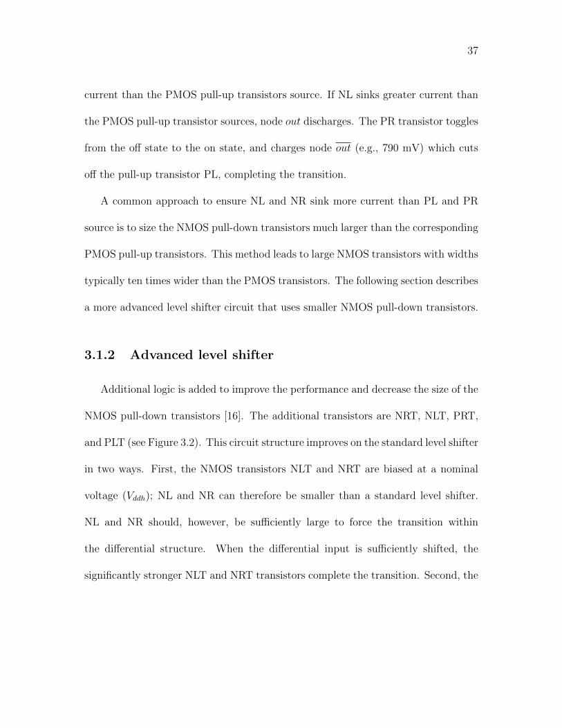
Additional logic is added to improve the performance and decrease the size of the
NMOS pull-down transistors [16]. The additional transistors are NRT, NLT, PRT,
and PLT (see Figure 3.2). This circuit structure improves on the standard level shifter
in two ways. First, the NMOS transistors NLT and NRT are biased at a nominal
voltage (Vddh); NL and NR can therefore be smaller than a standard level shifter.
NL and NR should, however, be sufficiently large to force the transition within
the differential structure. When the differential input is sufficiently shifted, the
significantly stronger NLT and NRT transistors complete the transition. Second, the
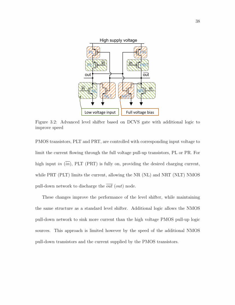
38
Low voltage input
High supply voltage
out out
in in NL NR
PL PR
NLT NRT
PLT PRT in in
Full voltage bias
Figure 3.2: Advanced level shifter based on DCVS gate with additional logic toimprove speed
PMOS transistors, PLT and PRT, are controlled with corresponding input voltage to
limit the current flowing through the full voltage pull-up transistors, PL or PR. For
high input in (in), PLT (PRT) is fully on, providing the desired charging current,
while PRT (PLT) limits the current, allowing the NR (NL) and NRT (NLT) NMOS
pull-down network to discharge the out (out) node.
These changes improve the performance of the level shifter, while maintaining
the same structure as a standard level shifter. Additional logic allows the NMOS
pull-down network to sink more current than the high voltage PMOS pull-up logic
sources. This approach is limited however by the speed of the additional NMOS
pull-down transistors and the current supplied by the PMOS transistors.

39
A novel level shifter that overcomes this issue of a strong PMOS pull-up network
is introduced in this chapter. This circuit is discussed in the following section.
3.2 Proposed wide voltage range level shifter for
near threshold circuits
The proposed level shifter is based on DCVS, similar to the standard level shift-
ing circuit described in Section 3.1. Rather than increasing the size of the NMOS
transistors, however, the proposed circuit dynamically changes the current sourced
by the relevant PMOS pull-up transistor (PL/PR) to ensure that the weak NMOS
pull-down transistor (NL/NR) sinks more current than the PMOS pull-up (PL/PR)
network sources. The proposed low voltage level shifter is illustrated in Figure 3.3a.
3.2.1 Structure of the proposed wide voltage range level
shifter
The novelty of this circuit topology is the feedback loop. The feedback loop
consists of a delay element that connects the output node D (high voltage domain)
to the input of two multiplexors, MUXL and MUXR. The delay element is based
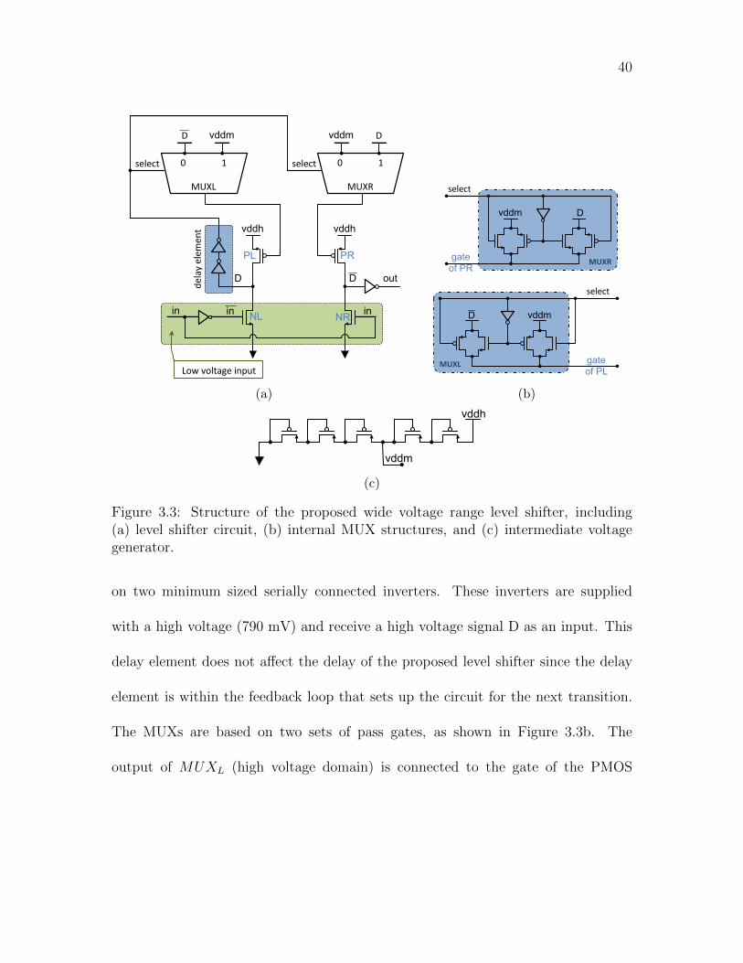
40
vddh
D
in NR
PR
D
in NL
PL
vddh
out
in
select
delay elem
ent
Low voltage input
MUXL
D vddm
0 1 select
MUXR
D vddm
0 1
(a)
MUXR gate of PR
D vddm
select
MUXL
D vddm
select
gate of PL
(b)
vddh
vddm
(c)
Figure 3.3: Structure of the proposed wide voltage range level shifter, including(a) level shifter circuit, (b) internal MUX structures, and (c) intermediate voltagegenerator.
on two minimum sized serially connected inverters. These inverters are supplied
with a high voltage (790 mV) and receive a high voltage signal D as an input. This
delay element does not affect the delay of the proposed level shifter since the delay
element is within the feedback loop that sets up the circuit for the next transition.
The MUXs are based on two sets of pass gates, as shown in Figure 3.3b. The
output of MUXL (high voltage domain) is connected to the gate of the PMOS

41
pull-up transistor PL. When select is high (high voltage domain), the gate of PL is
connected to the intermediate voltage Vddm which temporarily weakens PL. When
select is low, the gate of PL is connected to node D which preserves the differential
operation. Similarly, the output of MUXR is connected to the gate of the PMOS
pull-up transistor PR. When select is high, the gate of PR is connected to node
D which preserves the differential operation. When select is low, the gate of PR
is connected to the intermediate voltage Vddm, which temporarily weakens PR. An
example of this operation is described in Section 3.2.2.
This configuration eliminates the need for the large NMOS pull-down transistors,
NL and NR, because the relevant PMOS pull-up transistor is maintained at a low
voltage bias for the upcoming transition. This approach also greatly lowers the
transition time as compared to other level shifters.
Symmetric operation of the proposed level shifter is preserved over the maximum
operating range. Only minor balancing of the differential branches and the input
inverter is required due to the low contention between the pull-up PMOS transistors
and the pull-down NMOS transistors. During the falling transition, the input signal
propagates through a skewed inverter with a wider PMOS transistor to minimize
the charge time of the NL gate. Node D is discharged with low contention from PL,
which quickly turns on PR (as opposed to a standard high contention level shifter) to

42
charge the output. Alternatively, the rising input produces a faster transition since
the rising input lacks an inversion delay. This inversion delay is applied during the
rising transition by sizing NR smaller than NL (to maintain symmetry). Symmetric
operation of the proposed level shifter is exhibited mostly when operating close to
the maximum voltage range. With smaller voltage ranges (e.g., 0.5 volts to 0.79
volts and less), the symmetry degrades. The low contention between the PMOS and
NMOS transistors also contributes to the higher dynamic energy efficiency of the
proposed circuit as compared to other level shifters.
The intermediate voltage Vddm is generated by a voltage divider, as shown in
Figure 3.3c, which consists of five minimum sized diode connected PMOS transistors.
In this configuration, a stable bias voltage of 450 mV is generated to weaken, as
needed, the pull-up PMOS transistors.
The area overhead is comparable to the reference level shifters due to the smaller
area of the pull-down NMOS transistors. While the addition of the MUXs, delay
elements, and intermediate voltage generator introduce additional transistors, this
area is similar to the area required by the more complex pull-up network of the
reference level shifters.
As described in this section, the proposed level shifter exhibits higher performance
as compared to other level shifters. The speed improvement is due to the feedback
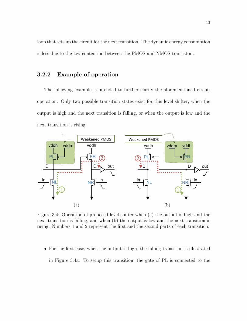
43
loop that sets up the circuit for the next transition. The dynamic energy consumption
is less due to the low contention between the PMOS and NMOS transistors.
3.2.2 Example of operation
The following example is intended to further clarify the aforementioned circuit
operation. Only two possible transition states exist for this level shifter, when the
output is high and the next transition is falling, or when the output is low and the
next transition is rising.
vddh
D
in NR
PR
D
in NL
PL
vddh
out
vddm
1
2
Weakened PMOS
(a)
D
in NR
PR
D
in NL
PL
out
vddh vddh vddm
1
2
Weakened PMOS
(b)
Figure 3.4: Operation of proposed level shifter when (a) the output is high and thenext transition is falling, and when (b) the output is low and the next transition isrising. Numbers 1 and 2 represent the first and the second parts of each transition.
• For the first case, when the output is high, the falling transition is illustrated
in Figure 3.4a. To setup this transition, the gate of PL is connected to the

44
intermediate supply voltage Vddm and the gate of PR is connected to node
D. This connection biases PL into the near cutoff region of operation which
degrades the drive strength of PL. Without contention from PL, as shown in
the figure, node D discharges through the pull-down network NL. As shown
in Figure 3.4a, node D is charged to the full voltage by the pull-up network
PR. After a delay, the feedback signal from node D propagates to the select
input of MUXL and MUXR (the feedback path shown in Figure 3.3a) which
is connected to the gate of PL and PR. This event sets up the state of the level
shifter for the next transition.
• The second case is presented in Figure 3.4b. In this transition, the level shifter
operates in the same way as described in the first case; however, each operation
is mirrored to the other differential branch. Node D is discharged through NR
while the current supplied by transistor PR is less due to the intermediate
supply voltage Vddm (connected to the gate of PR).
3.3 Evaluation of proposed level shifter
Evaluation of the proposed level shifter is described in this section. This evalua-
tion demonstrates the high speed and low energy consumption of the proposed level
45
shifter operating over a wide voltage range. Additionally, the proposed level shifter
is compared to other published level shifters.
3.3.1 Simulation setup
The speed and tolerance to variations at low voltage levels are arguably the most
important issues in near threshold circuits [16], [33]. To demonstrate the feasibility
of this level shifter for low voltage operation, the proposed circuit is validated against
statistical Monte Carlo analysis with 1,000 iterations. The Monte Carlo analysis is
applied for a range of standard corners, typical-typical (TT), slow-fast (SF), and
fast-slow (FS), at 125 ◦C and -30 ◦C. The low voltage input of the level shifter is
buffered with a pair of low voltage inverters to isolate the ideal voltage source and to
introduce variations. These input buffers also contribute a non-ideal input slew equal
to 60 ps, on average, for the maximum conversion range. The output of the level
shifter is connected to a fanout load of four (FO4), which consists of four identical
inverters supplied with a nominal voltage of 0.79 volts. This analysis is performed
on a pre-layout circuit; therefore, the simulation is supplied with a pre-extraction
netlist.
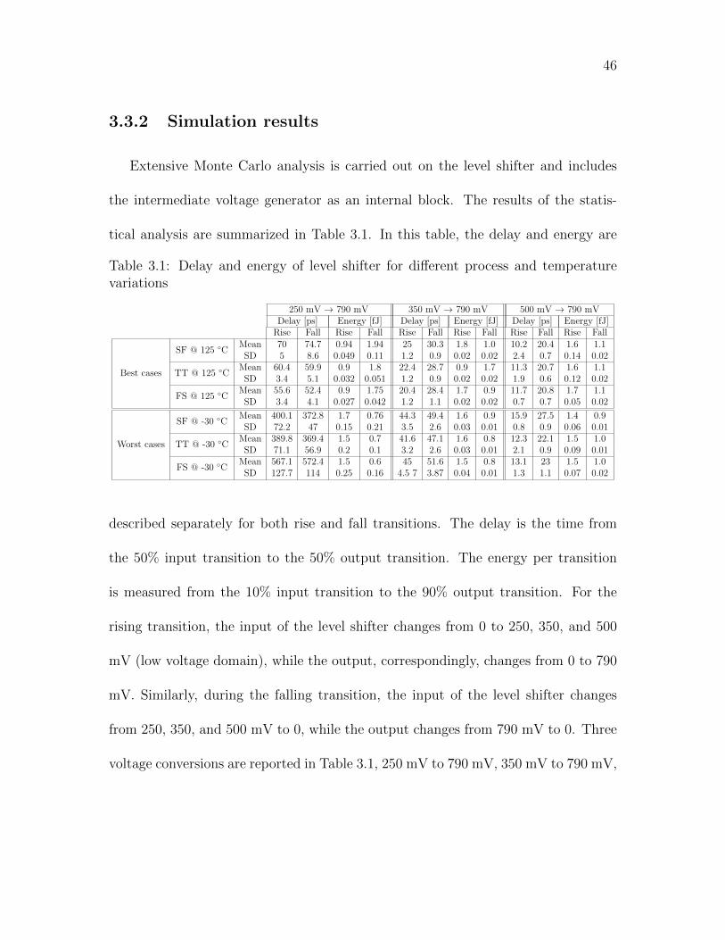
46
3.3.2 Simulation results
Extensive Monte Carlo analysis is carried out on the level shifter and includes
the intermediate voltage generator as an internal block. The results of the statis-
tical analysis are summarized in Table 3.1. In this table, the delay and energy are
Table 3.1: Delay and energy of level shifter for different process and temperaturevariations
250 mV → 790 mV 350 mV → 790 mV 500 mV → 790 mVDelay [ps] Energy [fJ] Delay [ps] Energy [fJ] Delay [ps] Energy [fJ]
Rise Fall Rise Fall Rise Fall Rise Fall Rise Fall Rise Fall
Best cases
SF @ 125 ◦CMean 70 74.7 0.94 1.94 25 30.3 1.8 1.0 10.2 20.4 1.6 1.1SD 5 8.6 0.049 0.11 1.2 0.9 0.02 0.02 2.4 0.7 0.14 0.02
TT @ 125 ◦CMean 60.4 59.9 0.9 1.8 22.4 28.7 0.9 1.7 11.3 20.7 1.6 1.1SD 3.4 5.1 0.032 0.051 1.2 0.9 0.02 0.02 1.9 0.6 0.12 0.02
FS @ 125 ◦CMean 55.6 52.4 0.9 1.75 20.4 28.4 1.7 0.9 11.7 20.8 1.7 1.1SD 3.4 4.1 0.027 0.042 1.2 1.1 0.02 0.02 0.7 0.7 0.05 0.02
Worst cases
SF @ -30 ◦CMean 400.1 372.8 1.7 0.76 44.3 49.4 1.6 0.9 15.9 27.5 1.4 0.9SD 72.2 47 0.15 0.21 3.5 2.6 0.03 0.01 0.8 0.9 0.06 0.01
TT @ -30 ◦CMean 389.8 369.4 1.5 0.7 41.6 47.1 1.6 0.8 12.3 22.1 1.5 1.0SD 71.1 56.9 0.2 0.1 3.2 2.6 0.03 0.01 2.1 0.9 0.09 0.01
FS @ -30 ◦CMean 567.1 572.4 1.5 0.6 45 51.6 1.5 0.8 13.1 23 1.5 1.0SD 127.7 114 0.25 0.16 4.5 7 3.87 0.04 0.01 1.3 1.1 0.07 0.02
described separately for both rise and fall transitions. The delay is the time from
the 50% input transition to the 50% output transition. The energy per transition
is measured from the 10% input transition to the 90% output transition. For the
rising transition, the input of the level shifter changes from 0 to 250, 350, and 500
mV (low voltage domain), while the output, correspondingly, changes from 0 to 790
mV. Similarly, during the falling transition, the input of the level shifter changes
from 250, 350, and 500 mV to 0, while the output changes from 790 mV to 0. Three
voltage conversions are reported in Table 3.1, 250 mV to 790 mV, 350 mV to 790 mV,
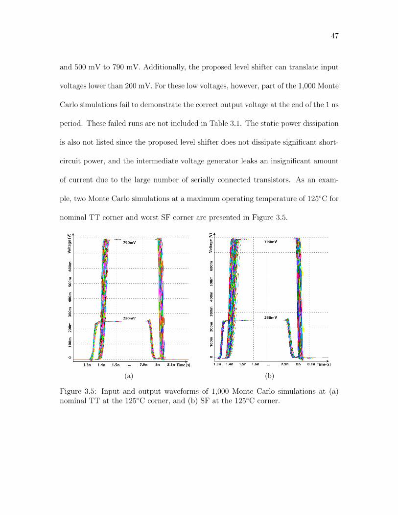
47
and 500 mV to 790 mV. Additionally, the proposed level shifter can translate input
voltages lower than 200 mV. For these low voltages, however, part of the 1,000 Monte
Carlo simulations fail to demonstrate the correct output voltage at the end of the 1 ns
period. These failed runs are not included in Table 3.1. The static power dissipation
is also not listed since the proposed level shifter does not dissipate significant short-
circuit power, and the intermediate voltage generator leaks an insignificant amount
of current due to the large number of serially connected transistors. As an exam-
ple, two Monte Carlo simulations at a maximum operating temperature of 125◦C for
nominal TT corner and worst SF corner are presented in Figure 3.5.
(a) (b)
Figure 3.5: Input and output waveforms of 1,000 Monte Carlo simulations at (a)nominal TT at the 125◦C corner, and (b) SF at the 125◦C corner.
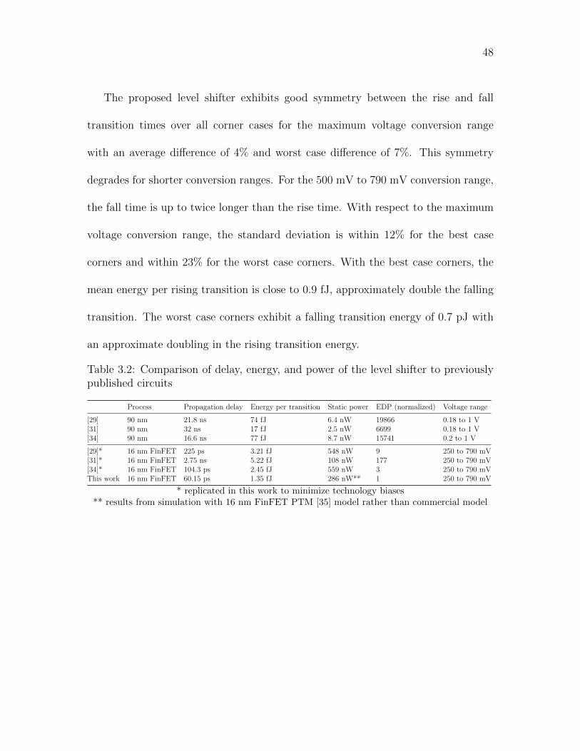
48
The proposed level shifter exhibits good symmetry between the rise and fall
transition times over all corner cases for the maximum voltage conversion range
with an average difference of 4% and worst case difference of 7%. This symmetry
degrades for shorter conversion ranges. For the 500 mV to 790 mV conversion range,
the fall time is up to twice longer than the rise time. With respect to the maximum
voltage conversion range, the standard deviation is within 12% for the best case
corners and within 23% for the worst case corners. With the best case corners, the
mean energy per rising transition is close to 0.9 fJ, approximately double the falling
transition. The worst case corners exhibit a falling transition energy of 0.7 pJ with
an approximate doubling in the rising transition energy.
Table 3.2: Comparison of delay, energy, and power of the level shifter to previouslypublished circuits
Process Propagation delay Energy per transition Static power EDP (normalized) Voltage range
[29] 90 nm 21.8 ns 74 fJ 6.4 nW 19866 0.18 to 1 V[31] 90 nm 32 ns 17 fJ 2.5 nW 6699 0.18 to 1 V[34] 90 nm 16.6 ns 77 fJ 8.7 nW 15741 0.2 to 1 V
[29]* 16 nm FinFET 225 ps 3.21 fJ 548 nW 9 250 to 790 mV[31]* 16 nm FinFET 2.75 ns 5.22 fJ 108 nW 177 250 to 790 mV[34]* 16 nm FinFET 104.3 ps 2.45 fJ 559 nW 3 250 to 790 mVThis work 16 nm FinFET 60.15 ps 1.35 fJ 286 nW** 1 250 to 790 mV
* replicated in this work to minimize technology biases** results from simulation with 16 nm FinFET PTM [35] model rather than commercial model
49
3.3.3 Comparison to previous works
The proposed level shifter is compared in Table 3.2 to the latest published level
converters [29], [31], [34]. To provide a fair comparison, these level shifters are
compared in two different ways. In the top part of Table 3.2, the reference converters
are presented with the originally published specifications. In the bottom part of Table
3.2, scaled versions of the same converters are presented. The reference level shifters
provide an added dimension to the comparison, demonstrating that the performance
gains of the proposed circuit are not only due to the advanced technology. These
converters are scaled to 16 nm FinFET technology and analyzed with 16 nm FinFET
PTM models [35] under the same conditions as the proposed level shifter. The 16 nm
FinFET PTM model does not support triple threshold voltage transistor models as
used in [31], [34], the replicated circuits are therefore evaluated with dual threshold
voltage transistor models. The same W/L ratios, as published in the referenced
papers, are maintained while the transistor length is scaled to 16 nm technology.
The proposed level shifter exhibits enhanced performance as compared to the
other published level shifters, as summarized in Table 3.2. In this table, the original
version of the referenced circuits presents a tradeoff among delay, energy, and static
power. The circuit described in [29] exhibits average speed and energy, while the
circuit described in [31] is slower but more energy efficient, and the circuit described
50
in [34] is faster but less energy efficient. When the reference circuits are replicated
using a 16 nm FinFET technology, the best reference circuit is the circuit described
in [34] (other than static power). Comparing the proposed level shifter to the level
shifter published in [34], the proposed level shifter exhibits 42% shorter delay, 45%
lower energy consumption, and 48% lower static power dissipation. The proposed
level shifter therefore provides significant performance advantages as compared to
these circuits.
3.4 Summary
The proposed level shifter is shown to be suitable for integration in sub-30 nm
multi-voltage domain microprocessors. Extensive Monte Carlo analysis demonstrates
that the proposed circuit reliably level shifts voltages between 250 mV and 790
mV. The proposed converter therefore supports near threshold circuits despite the
increased sensitivity to process variations. The converter maintains symmetric rise
and fall transition times over the maximum voltage conversion range across different
statistical corners (TT, FS, and SF at 125◦C and -30◦C). Additionally, the proposed
converter is compared to recently published level shifters and exhibits significant
improvements in speed, energy, and power efficiency.
51
Chapter 4
Interconnect Model for WideSupply Voltage Range RepeaterInsertion
During the past decade, the microelectronics industry has shifted focus to mobile
platforms as the personal computing standard. These battery powered devices em-
phasize energy efficiency in modern sub-22 nm CMOS technologies [9]. Techniques to
reduce power consumption include reducing the supply voltage due to the quadratic
dependence on power consumption. In those cases where high speed operation is
not required, the supply voltage is reduced to near the threshold voltage. Circuits
that operate near the threshold voltage benefit from higher energy efficiency due to
a balance between dynamic and static power consumption [36]. In extreme cases
where minimum power consumption is required, the supply voltage is reduced into
the subthreshold region. In this region of operation, the dynamic power is sufficiently
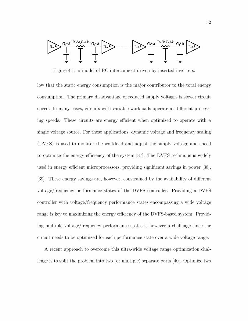
52
Figure 4.1: π model of RC interconnect driven by inserted inverters.
low that the static energy consumption is the major contributor to the total energy
consumption. The primary disadvantage of reduced supply voltages is slower circuit
speed. In many cases, circuits with variable workloads operate at different process-
ing speeds. These circuits are energy efficient when optimized to operate with a
single voltage source. For these applications, dynamic voltage and frequency scaling
(DVFS) is used to monitor the workload and adjust the supply voltage and speed
to optimize the energy efficiency of the system [37]. The DVFS technique is widely
used in energy efficient microprocessors, providing significant savings in power [38],
[39]. These energy savings are, however, constrained by the availability of different
voltage/frequency performance states of the DVFS controller. Providing a DVFS
controller with voltage/frequency performance states encompassing a wide voltage
range is key to maximizing the energy efficiency of the DVFS-based system. Provid-
ing multiple voltage/frequency performance states is however a challenge since the
circuit needs to be optimized for each performance state over a wide voltage range.
A recent approach to overcome this ultra-wide voltage range optimization chal-
lenge is to split the problem into two (or multiple) separate parts [40]. Optimize two
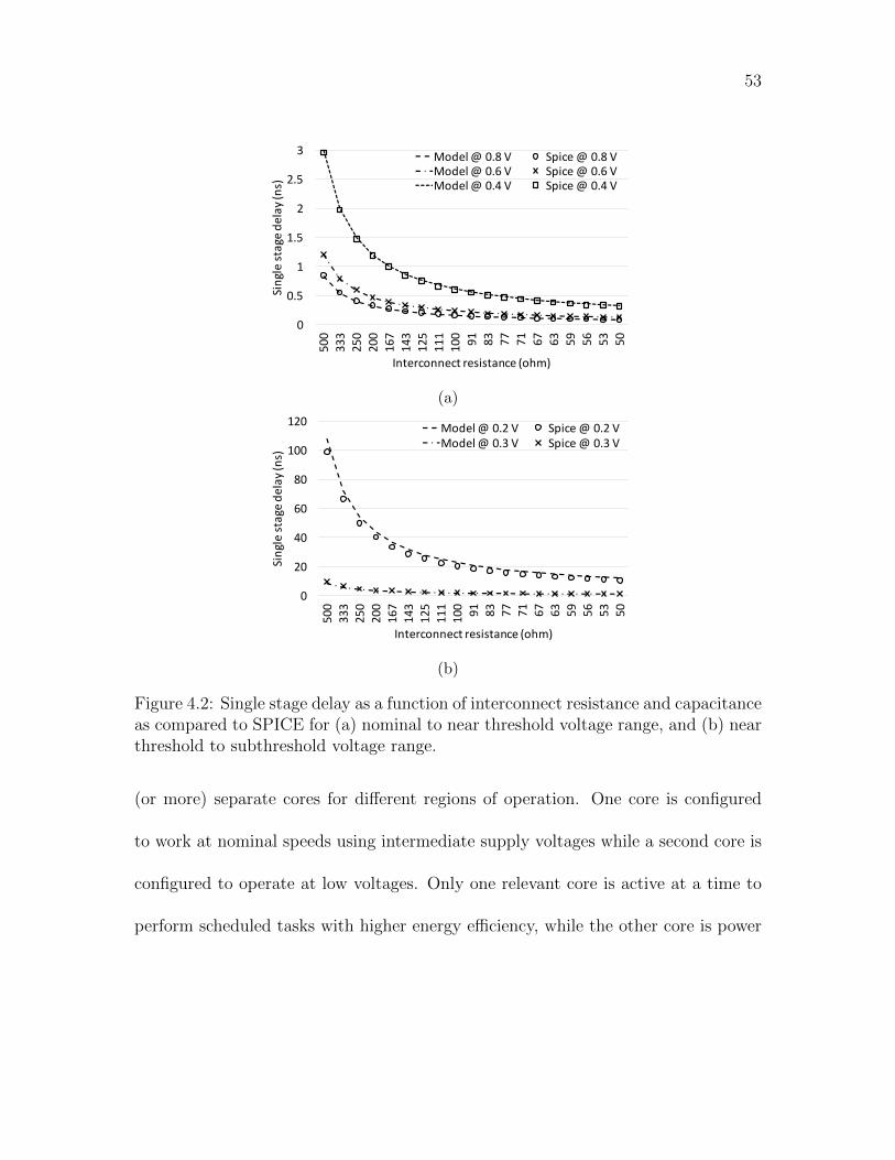
53
0
0.5
1
1.5
2
2.5
3
500
333
250
200
167
143
125
111
100 91 83 77 71 67 63 59 56 53 50
Singlestagede
lay(ns)
Interconnectresistance(ohm)
[email protected] [email protected]@0.6V [email protected]@0.4V [email protected]
(a)
0
20
40
60
80
100
120
500
333
250
200
167
143
125
111
100 91 83 77 71 67 63 59 56 53 50
Singlestagede
lay(ns)
Interconnectresistance(ohm)
[email protected] [email protected]@0.3V [email protected]
(b)
Figure 4.2: Single stage delay as a function of interconnect resistance and capacitanceas compared to SPICE for (a) nominal to near threshold voltage range, and (b) nearthreshold to subthreshold voltage range.
(or more) separate cores for different regions of operation. One core is configured
to work at nominal speeds using intermediate supply voltages while a second core is
configured to operate at low voltages. Only one relevant core is active at a time to
perform scheduled tasks with higher energy efficiency, while the other core is power
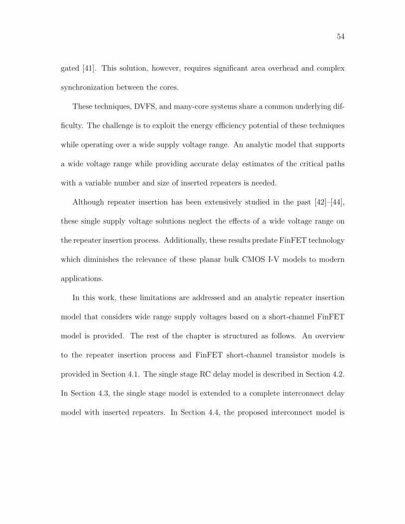
54
gated [41]. This solution, however, requires significant area overhead and complex
synchronization between the cores.
These techniques, DVFS, and many-core systems share a common underlying dif-
ficulty. The challenge is to exploit the energy efficiency potential of these techniques
while operating over a wide supply voltage range. An analytic model that supports
a wide voltage range while providing accurate delay estimates of the critical paths
with a variable number and size of inserted repeaters is needed.
Although repeater insertion has been extensively studied in the past [42]–[44],
these single supply voltage solutions neglect the effects of a wide voltage range on
the repeater insertion process. Additionally, these results predate FinFET technology
which diminishes the relevance of these planar bulk CMOS I-V models to modern
applications.
In this work, these limitations are addressed and an analytic repeater insertion
model that considers wide range supply voltages based on a short-channel FinFET
model is provided. The rest of the chapter is structured as follows. An overview
to the repeater insertion process and FinFET short-channel transistor models is
provided in Section 4.1. The single stage RC delay model is described in Section 4.2.
In Section 4.3, the single stage model is extended to a complete interconnect delay
model with inserted repeaters. In Section 4.4, the proposed interconnect model is
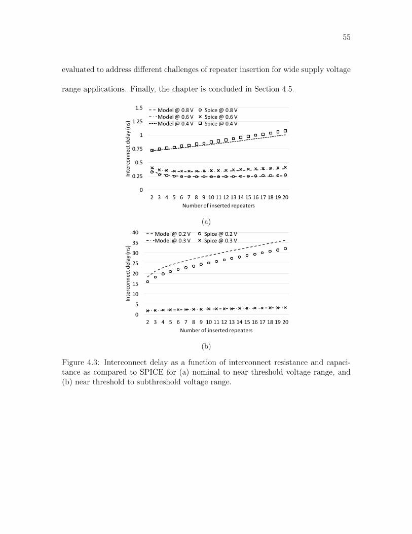
55
evaluated to address different challenges of repeater insertion for wide supply voltage
range applications. Finally, the chapter is concluded in Section 4.5.
0
0.25
0.5
0.75
1
1.25
1.5
2 3 4 5 6 7 8 9 10 11 12 13 14 15 16 17 18 19 20
Intercon
nectdelay(ns)
Numberofinsertedrepeaters
[email protected] [email protected]@0.6V [email protected]@0.4V [email protected]
(a)
0
5
10
15
20
25
30
35
40
2 3 4 5 6 7 8 9 10 11 12 13 14 15 16 17 18 19 20
Intercon
nectdelay(ns)
Numberofinsertedrepeaters
[email protected] [email protected]@0.3V [email protected]
(b)
Figure 4.3: Interconnect delay as a function of interconnect resistance and capaci-tance as compared to SPICE for (a) nominal to near threshold voltage range, and(b) near threshold to subthreshold voltage range.
56
4.1 Existing FinFET transistor and Interconnect
Delay Models
The interconnect resistance in deeply scaled sub-22 nm technologies is increasing
with each technology node due to longer distances and smaller cross sectional areas.
To optimize the propagation delay through a resistive line, a repeater insertion tech-
nique is required that breaks the large resistance into sections. The repeater insertion
technique proposed here is based on an interconnect delay model with repeaters that
considers a wide supply voltage range. This wide supply voltage range delay model
is based on the RC delay expression and FinFET transistor drain current models
described in this section.
Consider the wire depicted in Figure 4.1. The resistance and capacitance of the
wire are represented by a π model with repeaters inserted to partition the large
resistance. A single π section is used to model each stage with good accuracy [45].
A closed-form model of the delay of a single stage includes the driving inverter, an
RC π model of the interconnect, and the input capacitance of the following stage.
This system has been previously demonstrated on a linearized α-power law model of
a planar bulk transistor [43]. For FinFET technology, however, this solution is not
practical due to the lack of a linear FinFET transistor current model. To overcome
57
this problem, the RC delay model of (4.1) developed by Sakurai [46] is used here.
td(vr)
RC= 0.1 + ln(
1
1− vr)(RTCT +RT + CT + 0.4), (4.1)
RT = rt/R, (4.2)
CT = ct/C, (4.3)
vr = V (out)/Vdd. (4.4)
In (4.1), rt and ct are, respectively, the resistance of the driving transistor and the
input capacitance of the next stage (the gate capacitance of an inverter). The ratio
of the output voltage at time tvr over the supply voltage (Vdd) is vr, and R and C
are, respectively, the resistance and capacitance of the interconnect. This RC delay
model is widely used and provides high accuracy [46].
Although a number of analytic current models of FinFET transistors are available
[47]–[50], these models either do not provide a closed-form expression or consider only
long channel effects. The equivalent resistance (rt) of the driving transistor is based
on the short-channel FinFET transistor model of (4.5) [50] which considers inversion
sheet charge densities (Qis and Qid),
ID = 4µ02W
LV 2therm[(Qis −Qid) + 1/2(Q2
is −Q2id)]. (4.5)

58
This short-channel FinFET model provides sufficient accuracy for deeply scaled sub-
22 nm technologies commonly used in industry.
4.2 Single stage delay in wide supply voltage range
applications
A single stage delay model of a CMOS inverter driving an RC load is described in
this section. The single stage consists of an inverter driving a parasitic interconnect
impedance and the input capacitance of the next stage. The model considers the
discharge time through the NMOS FinFET transistor, and leakage current through
the complementary PMOS transistor.
The single stage delay across a wide supply voltage range is
tsingle stage(vr) = (4.6)
0.1RC − ln(1− vr)(RTCT +RT + CT + 0.4)RC
+ Fwv(R,mul, Vdd).
This model consists of two major parts. The first term of (4.6) is the delay as a
function of the nominal voltage as described by Sakurai in (4.1). The second term,
59
Fwv, as described in this section, provides the wide supply voltage range dependent
component by relating the interconnect resistance R and repeater size multiplier
mul across a wide range of Vdd. This additional term is required since the RT
ratio in the first term describes the delay assuming a constant resistance of the
driving transistor as opposed to a dynamically changing resistance over the transition
duration. Additionally, the first term describes the delay at a nominal operating
voltage as opposed to over a wide range of supply voltages. The wide voltage term,
however, is not an explicit function of interconnect or load capacitance since these
quantities remain constant with changes in the supply voltage and are considered
within the first term of (4.6).
The equivalent transistor resistance rt in the single stage delay model is based on
the FinFET I-V model of (4.5) with Vth ≈ 380 mV . The maximum resistance over
the entire range of VDS for a target gate voltage is
rt(VGS) = max{ VDSID(VGS, VDS)
, VDS = 0 . . . Vdd}. (4.7)
The maximum resistance for each VGS provides greater accuracy over a wide range of
supply voltages as compared to a minimum, average, or weighted average resistance
60
[45]. The input gate capacitance is
ct(mul, nfin,Weff) = 4mul × nfin× Cox× L×Weff, (4.8)
and includes both of the PMOS and NMOS transistors of an inverter with a size
multiplier mul, number of fins nfin, effective width Weff = Hfin +Wfin/2, and length
L.
The wide supply voltage range component of (4.6) is
Fwv(mul,R, Vdd) = αR2 + βR + γ, (4.9)
where α, β, and γ are fitting coefficients that characterize the disparity between
the simulated delay and the delay provided in (4.1) as a quadratic function of R.
This term supports a wide supply voltage range, and reduces the error assuming a
constant equivalent resistance of the driving transistor. The coefficients α, β, and γ,
respectively, (4.10), (4.11), and (4.12), compensate for the nonlinearity due to the
constant resistance of the transistor as a function of the transistor size multiplier
61
mul and the supply voltage.
α = −3.8624× 10⁻¹⁷, (4.10)
β = −1.892× 10⁻¹³ × V −3.379dd ×mulδ, (4.11)
γ = 6.26× 10⁻¹⁴ × [V −2.085dd ln(mul)− 12.46V −1.743dd ], (4.12)
δ = −1.629V 2dd + 1.737Vdd − 1.468. (4.13)
Fwv(mul,R, Vdd) supports a supply voltage range, ranging from 0.8 volts to 0.4 volts.
The voltage range, however, can be further expanded to a wide supply voltage range
including the near threshold and subthreshold regions from 0.4 volts to 0.2 volts. In
this voltage range, the coefficients β, γ, and δ are, respectively,
β = −2.348× 10⁻¹⁴ × [V −5.603dd ×mulδ + 1], (4.14)
γ = 2.194× 10⁻¹⁵ × [V −5.5047dd ln(mul)− 22.62V −4.742dd ], (4.15)
δ = 2.43V 2dd − 1.58Vdd − 0.7874. (4.16)
The single stage delay model is validated across an extended range of repeater
sizes, interconnect resistances and capacitances, and supply voltages. The error of the
analytic delay as compared to simulation ranges between 7.3% to -3.5% for nominal
62
to near threshold voltages. For an extended voltage range that includes subthreshold
voltages, the error ranges from 13% to -12%. The error as a function of interconnect
resistance is shown in Figure 4.2.
4.3 Interconnect delay model
An analytic model of the interconnect delay considering a wide supply voltage
range is described in this section. The proposed interconnect delay model is an
extension of the single stage model described in Section 4.2 for a number of stages.
This delay model assumes that a stage starts to transition once the input passes the
50% voltage level. vr is larger than 50% to compensate for the instantaneous input
transition in (4.1).
The contribution of the first stage tfirst = tsingle stage(0.6), intermediate stage
tintermediate = tsingle stage(0.68), and last stage tlast = tsingle stage(0.6) yields the total
delay of the interconnect with N inserted repeaters,
TD total = tfirst + (N − 2)× (tintermediate) + tlast. (4.17)
Note that the rise and fall delays are not separated since the same single stage model
provides the delay for rising and falling transitions, as described in Section 4.2.
63
This model is validated against SPICE, as depicted in Figure 4.3. Although only a
subset of the results is provided in the figure, the model exhibits good accuracy across
the entire parameter space. For nominal to near threshold voltages, the proposed
model exhibits an error between 9% to -17%. For near threshold to subthreshold
voltages, the proposed model exhibits an error between 17% to -15%.
4.4 Repeater insertion for wide supply voltage range
applications
In this section, challenges of the repeater insertion technique for wide supply
voltages are discussed. The optimal number of repeaters as a function of supply
voltage is described in Section 4.4.1. The effect on the delay for varying supply
voltages for a specific number of repeaters is discussed in Section 4.4.2. The maximum
range of supply voltages considering delay constraints is described in Section 4.4.3.
4.4.1 Optimal number of repeaters across a range of supply
voltages
The primary challenge of repeater insertion considering a wide supply voltage
range is the conflicting number and size of the inserted inverters needed for different
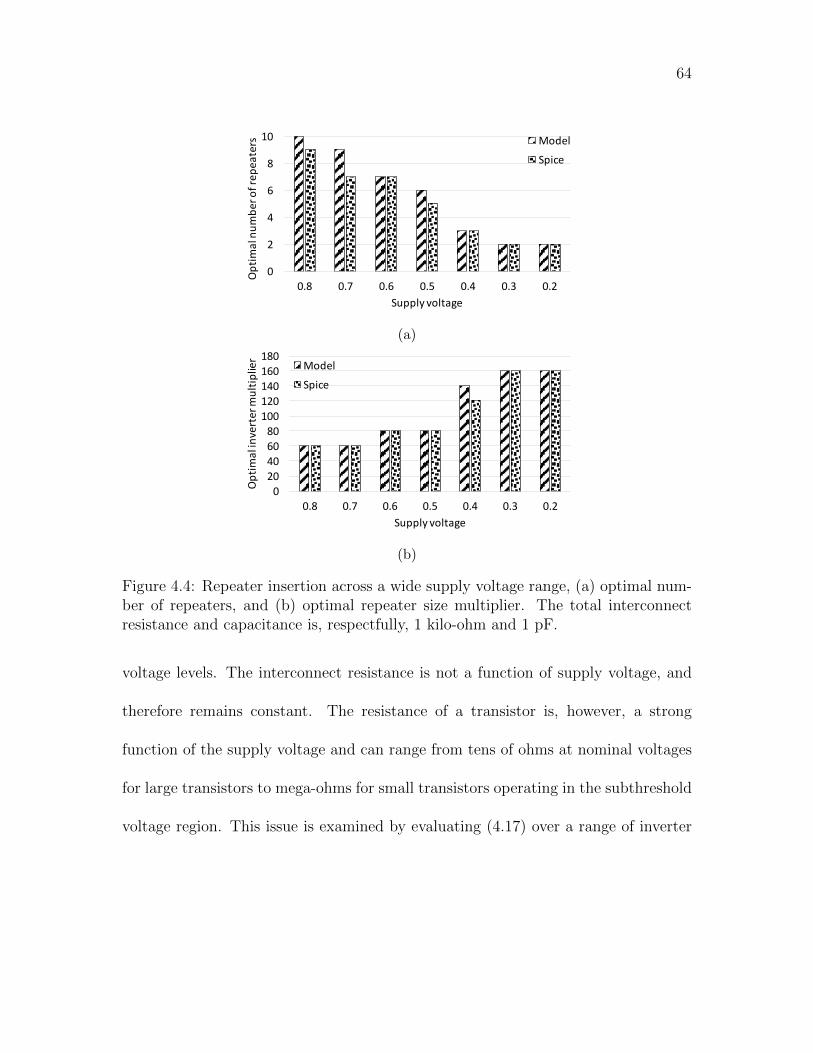
64
0
2
4
6
8
10
0.8 0.7 0.6 0.5 0.4 0.3 0.2
Optim
alnum
bero
frep
eaters
Supplyvoltage
ModelSpice
(a)
020406080100120140160180
0.8 0.7 0.6 0.5 0.4 0.3 0.2
Optim
alinvertermultip
lier
Supplyvoltage
ModelSpice
(b)
Figure 4.4: Repeater insertion across a wide supply voltage range, (a) optimal num-ber of repeaters, and (b) optimal repeater size multiplier. The total interconnectresistance and capacitance is, respectfully, 1 kilo-ohm and 1 pF.
voltage levels. The interconnect resistance is not a function of supply voltage, and
therefore remains constant. The resistance of a transistor is, however, a strong
function of the supply voltage and can range from tens of ohms at nominal voltages
for large transistors to mega-ohms for small transistors operating in the subthreshold
voltage region. This issue is examined by evaluating (4.17) over a range of inverter
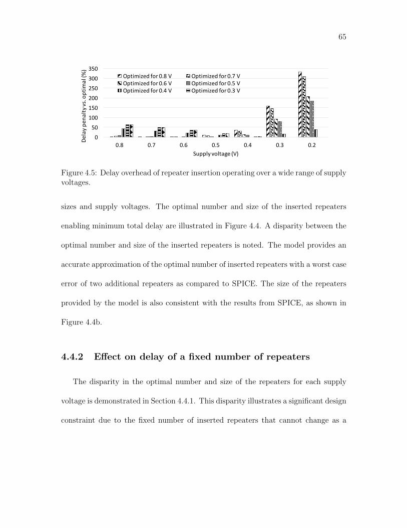
65
050100150200250300350
0.8 0.7 0.6 0.5 0.4 0.3 0.2
Delaype
nalty
vs.optim
al(%
)
Supplyvoltage(V)
Optimizedfor0.8V Optimizedfor0.7VOptimizedfor0.6V Optimizedfor0.5VOptimizedfor0.4V Optimizedfor0.3V
Figure 4.5: Delay overhead of repeater insertion operating over a wide range of supplyvoltages.
sizes and supply voltages. The optimal number and size of the inserted repeaters
enabling minimum total delay are illustrated in Figure 4.4. A disparity between the
optimal number and size of the inserted repeaters is noted. The model provides an
accurate approximation of the optimal number of inserted repeaters with a worst case
error of two additional repeaters as compared to SPICE. The size of the repeaters
provided by the model is also consistent with the results from SPICE, as shown in
Figure 4.4b.
4.4.2 Effect on delay of a fixed number of repeaters
The disparity in the optimal number and size of the repeaters for each supply
voltage is demonstrated in Section 4.4.1. This disparity illustrates a significant design
constraint due to the fixed number of inserted repeaters that cannot change as a

66
function of voltage. When dealing with dynamically changing supply voltages, the
interconnect being optimized for a specific operating point exhibits different delay
overheads. A significant challenge is to determine the performance state that exhibits
the lower delay overhead. The proposed interconnect model of (4.17) characterizes
the delay penalty when optimizing the interconnect for a single supply voltage. From
this model, the optimal supply voltage that minimizes the delay overhead can be
determined, providing design guidelines for optimizing interconnect operating over a
wide range of supply voltages.
As shown in Figure 4.5, two primary observations can be drawn from this analysis.
The minimum delay overhead occurs at the 0.4 volt performance state, with three
repeaters with a size multiplier of 140. With this configuration, the average delay
overhead across the entire voltage range is 22.7%. Optimizing the low supply voltage
provides a smaller delay overhead at high voltages.
4.4.3 Maximum supply voltage range with delay constraint
The resistive and capacitive interconnect should be optimized at lower supply
voltages to enable higher frequency of operation across a wide range of supply volt-
ages, as described in Section 4.4.2. This condition does not hold when an external
delay constraint is imposed. The delay expression in Section 4.4.1 is presented as a
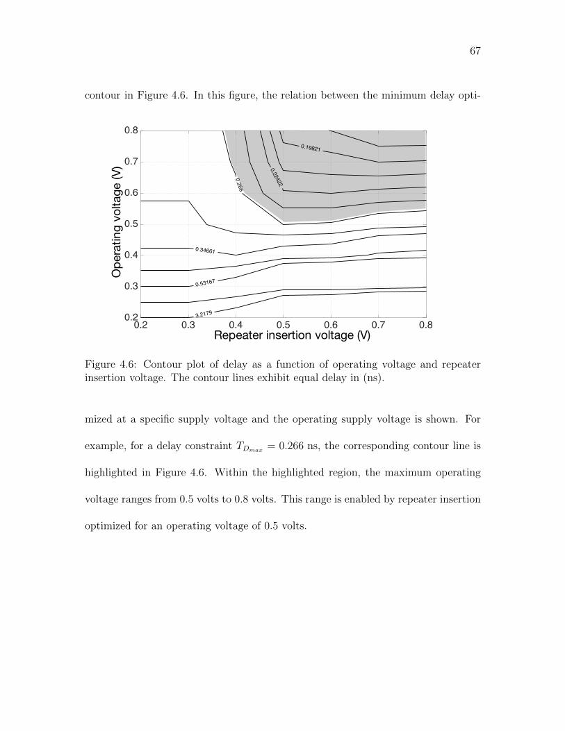
67
contour in Figure 4.6. In this figure, the relation between the minimum delay opti-
0.19821
0.22422
0.266
0.34661
0.53167
3.2179
0.2 0.3 0.4 0.5 0.6 0.7 0.8Repeater insertion optimized voltage (V)
0.2
0.3
0.4
0.5
0.6
0.7
0.8O
pera
ting
volta
ge (V
)O
pera
ting
volta
ge (V
)
Repeater insertion voltage (V)
Figure 4.6: Contour plot of delay as a function of operating voltage and repeaterinsertion voltage. The contour lines exhibit equal delay in (ns).
mized at a specific supply voltage and the operating supply voltage is shown. For
example, for a delay constraint TDmax = 0.266 ns, the corresponding contour line is
highlighted in Figure 4.6. Within the highlighted region, the maximum operating
voltage ranges from 0.5 volts to 0.8 volts. This range is enabled by repeater insertion
optimized for an operating voltage of 0.5 volts.

68
4.5 Summary
A closed-form model of interconnect delay with inserted repeaters supporting
a wide supply voltage range in sub-22 nm FinFET technologies is provided in this
chapter. Utilizing this delay model, design issues relating to repeater insertion over a
wide range of supply voltages are also addressed. The conflicting number and size of
repeaters required at different supply voltages is examined. To overcome this issue,
a method for optimizing the number and size of inserted repeaters across a wide
supply voltage range is proposed. The maximum attainable supply voltage range is
also provided considering delay constraints.
The proposed delay model is validated against a 14 nm commercial SPICE model.
The single stage delay model exhibits an accuracy ranging from 7.3% to -3.5% for
nominal to near threshold voltages. For an extended voltage range that includes
subthreshold voltages, the error increases to within 13% to -12%. The interconnect
delay model with inserted repeaters exhibits an error ranging between -17% to 9%
for nominal to near threshold voltages. For extended voltage range to subthreshold
voltages, the error increases to -15% to 17%. The proposed delay model is suitable
to address energy efficiency challenges in modern sub-22 nm FinFET technologies.
69
Chapter 5
MOS current mode logic nearthreshold circuits
The power consumption and speed are two primary characteristics of high per-
formance integrated circuits [9]. In this chapter, both of these characteristics are
addressed by utilizing low power near threshold circuits (NTC) [16] in combination
with high speed MOS current mode logic (MCML) [20]. The combination of MCML
with NTC produces a balanced circuit methodology that compensates for the vul-
nerable aspects while benefiting from the advantages of each technology.
The chapter is structured as follows. In Section 5.1, NTC and MCML are pre-
sented. The benefits of combining MCML with NTC are described in Section 5.2.
The simulation environment is reviewed in Section 5.3, and the results are provided
in Section 5.4. The chapter is summarized in Section 5.5.

70
5.1 Background
Combining MOS current mode logic with near threshold circuits is proposed in
this chapter. Each technology is individually described in Chapter 2 and this section
to provide a basis for the combination presented in Section 5.2. Near threshold
circuits are discussed in Chapter 2, and MCML is described in Section 5.1.1.
5.1.1 MCML circuits
MCML is the CMOS counterpart of bipolar emitter coupled logic (ECL), which
has been in use in high speed applications since the 1970s. MCML maintains the
benefits of traditional ECL, such as high speed, reduction in dI/dt noise, and common
mode noise rejection, without requiring bipolar transistors [51].
An ideal MCML gate is shown in Figure 5.1. The gate is composed of three
parts: the pull-up load resistors, the pull-down logic network, and a constant current
source. The pull-up load resistors are typically PMOS transistors, as depicted in
Figure 5.2 for an MCML universal gate. PMOS transistors are used in the pull-up
network, similar to standard CMOS. During the low-to-high transition, the PMOS
pull-up network charges the output to VDD, unlike NMOS that charges the output
to VDD − Vth.
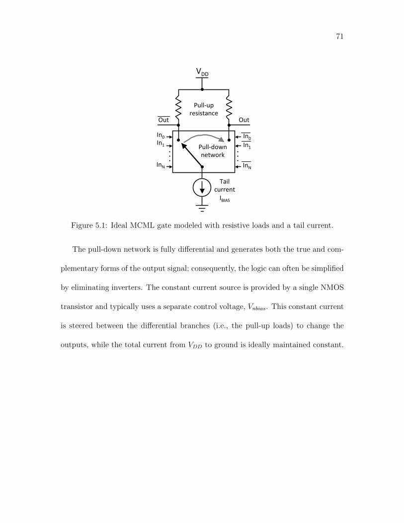
71
In0
In1
InN
Out
In0 In1
InN
Out
Tail current IBIAS
Pull-‐down network
Pull-‐up resistance
VDD
Figure 5.1: Ideal MCML gate modeled with resistive loads and a tail current.
The pull-down network is fully differential and generates both the true and com-
plementary forms of the output signal; consequently, the logic can often be simplified
by eliminating inverters. The constant current source is provided by a single NMOS
transistor and typically uses a separate control voltage, Vnbias. This constant current
is steered between the differential branches (i.e., the pull-up loads) to change the
outputs, while the total current from VDD to ground is ideally maintained constant.
72
5.1.1.1 Power efficiency of MCML
The power consumed by an MCML gate is
PMCML = IBIAS × VDD. (5.1)
Note that the power consumed by an MCML gate does not depend on the operating
frequency. In other words, an MCML gate consumes constant current (and power)
from the power supply network independent of the logic activity or frequency. This
behavior is in contrast to the CV 2f power dissipated by conventional CMOS, where
the power consumed by a static CMOS gate exhibits a linear relationship with op-
erating frequency. MCML is therefore more power efficient at high frequencies than
static CMOS. Standard MCML circuits operating under nominal conditions exhibit
enhanced power efficiency at frequencies above 5 GHz. At these frequencies, MCML,
although more power efficient than standard CMOS above 5 GHz suffers from high
power densities not acceptable in modern ultra-mobile microprocessors. To reduce
the frequency at which MCML dissipates less power than static CMOS, MCML
circuits are operated near the threshold voltage, as suggested in this chapter. By
combining MCML with NTC technology, the frequency at which MCML dissipates
less power than standard CMOS can be lowered to around 1 GHz, as shown in Figure
73
5.7.
5.1.1.2 High speed of MCML
MOS current mode logic operates at frequencies significantly higher than standard
CMOS. These frequencies are achieved due to the low delay of MCML. This property
of MCML circuits is largely due to the reduced voltage swing of MCML gates. The
voltage swing of an MCML gate is commonly two to ten times lower than VDD,
resulting in higher circuit speeds as compared to standard CMOS [52].
5.1.1.3 Low noise environment of MCML
CMOS circuits suffer from simultaneous switching noise (SSN), a significant
source of on-chip noise [21]. In contrast, the near constant current of MCML (regard-
less of the state, i.e., idle, transition, active) produces significantly less on-chip SSN.
The low noise of MCML is particularly relevant when combined with NTC due to the
exponential sensitivity of NTC circuits to the power supply when operating near the
threshold voltage [14]. In this chapter, the simultaneous switching noise generated
by MCML NTC circuits is shown to be ten times less noise than in standard CMOS
with NTC circuits. A noise analysis of these circuits is described in Section 5.4.2.
74
5.1.1.4 Logic gates
The design process of MCML circuits is more complex than standard CMOS.
Circuit parameters such as the supply voltage, voltage swing, pull-up equivalent re-
sistance, tail current, and input network need to be considered. These parameters are
correlated. A change in one parameter leads to adjustments in the other parameters.
For example, the voltage that determines the low output is a function of both the
supply voltage and voltage swing of the gate. The voltage swing affects the pull-up
resistance and tail current. If the tail current is chosen for a low power operating
point, the voltage swing is affected if the pull-up resistance is not modified. This
behavior is in contrast to standard CMOS gates which have fewer design parameters
(e.g., supply voltage, transistor sizes, and threshold voltage) and each parameter
independently affects the operating point. The use of high threshold voltage tran-
sistors rather than standard transistors to set a low power operating point does not
change the output swing of the gate.
To overcome this limitation of MCML technology, a family of logic gates have
been designed based on universal MCML gates [53]. This approach standardizes and
simplifies the process of MCML logic design to a small number of universal gates.
This capability is possible because basic MCML gates (i.e., NAND, AND, NOR,
and OR) only differ in the input and output connections. These basic MCML gates
75
share a common circuit topology, also referred to as a universal gate structure. This
universal gate structure can be either symmetric or asymmetric, depending upon the
set of gates that use this universal gate structure as well as power, speed, and area
constraints. The asymmetric universal gate structure of NAND and NOR gates is
illustrated in Figure 5.2 [9], [53]. As shown in this figure, the only difference between
these gates are the input and output connections. The lack of symmetry in this
universal gate structure leads to asymmetric rise and fall times. An asymmetric
universal gate structure however has two fewer input transistors and wires.
This set of basic gates can be further expanded to include an XOR gate if a
symmetric topology is considered. An MCML XOR gate is shown in Figure 5.3b
to illustrate a symmetric universal gate structure [9]. Other basic gate types (such
as NAND, AND, NOR, and OR) use this symmetric universal gate topology with
modified input and output connections. The drawback of a symmetric universal
gate is the increased area. A symmetric universal gate structure exhibits symmetric
rise and fall transitions and is simpler to design due to the symmetry of the circuit
structure. The symmetry enables the use of equal sized transistors in both the left
and right branches of the logic gate, eliminating the need to balance the branch
currents.
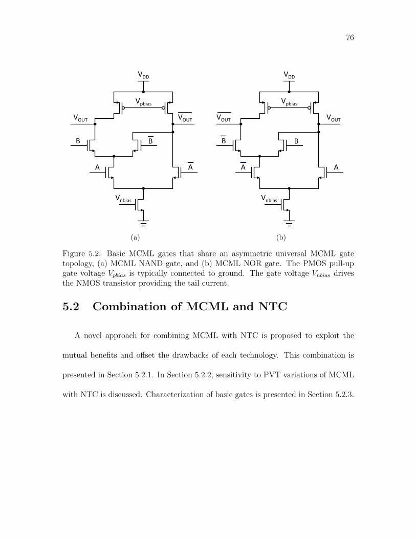
76
B
A A
B
Vnbias
VOUT
Vpbias
VDD
VOUT
(a)
B
A A
B
Vnbias
VOUT
Vpbias
VDD
VOUT
(b)
Figure 5.2: Basic MCML gates that share an asymmetric universal MCML gatetopology, (a) MCML NAND gate, and (b) MCML NOR gate. The PMOS pull-upgate voltage Vpbias is typically connected to ground. The gate voltage Vnbias drivesthe NMOS transistor providing the tail current.
5.2 Combination of MCML and NTC
A novel approach for combining MCML with NTC is proposed to exploit the
mutual benefits and offset the drawbacks of each technology. This combination is
presented in Section 5.2.1. In Section 5.2.2, sensitivity to PVT variations of MCML
with NTC is discussed. Characterization of basic gates is presented in Section 5.2.3.
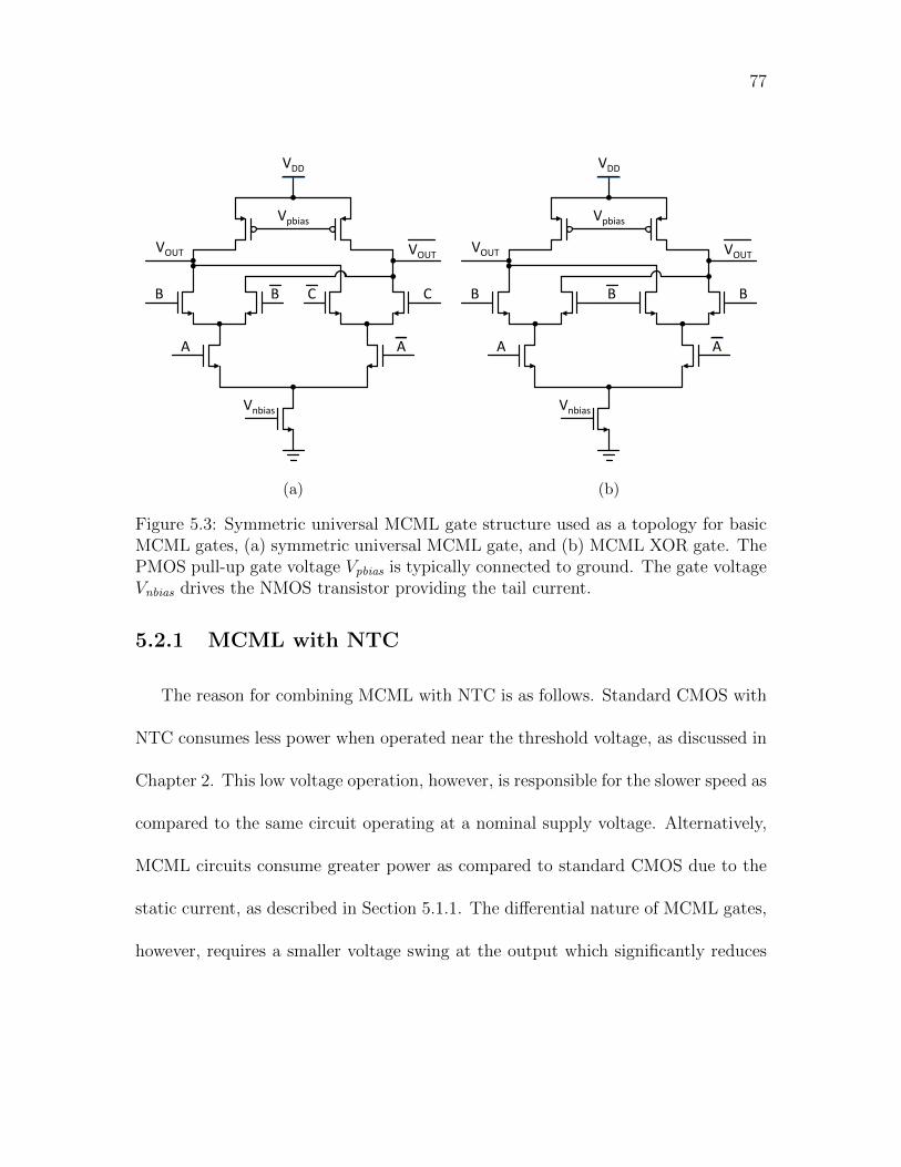
77
B
A A
B
Vnbias
VOUT
Vpbias
VDD
VOUT
C C
(a)
B
A A
B
Vnbias
VOUT
Vpbias
VDD
VOUT
B
(b)
Figure 5.3: Symmetric universal MCML gate structure used as a topology for basicMCML gates, (a) symmetric universal MCML gate, and (b) MCML XOR gate. ThePMOS pull-up gate voltage Vpbias is typically connected to ground. The gate voltageVnbias drives the NMOS transistor providing the tail current.
5.2.1 MCML with NTC
The reason for combining MCML with NTC is as follows. Standard CMOS with
NTC consumes less power when operated near the threshold voltage, as discussed in
Chapter 2. This low voltage operation, however, is responsible for the slower speed as
compared to the same circuit operating at a nominal supply voltage. Alternatively,
MCML circuits consume greater power as compared to standard CMOS due to the
static current, as described in Section 5.1.1. The differential nature of MCML gates,
however, requires a smaller voltage swing at the output which significantly reduces
78
the gate delay. CMOS with NTC therefore dissipates less power but operates at lower
speed, while standard MCML technology provides enhanced speed but consumes a
constant high power during both active and idle periods.
Therefore, MCML and NTC uncombined either dissipates excessive power or is
too slow. When combined, the constant power consumption of MCML is reduced to
much lower levels, producing an effective circuit topology. Additionally, the low noise
advantages of MCML, as described in Section 5.1.1, are maintained in the combined
circuit topology.
One issue however remains partly unresolved by this combination, the high sen-
sitivity of MCML NTC to PVT variations. This difficulty is discussed with greater
details in Section 5.2.2.
The advantages and disadvantages of combining both circuit approaches are sum-
marized in Table 5.1. In this table, as discussed in Sections 2.1.2, 5.1.1, and 5.2, the
speed of MCML with NTC is comparable to the speed of standard CMOS . The
energy is approximately one order of magnitude less than standard CMOS; however,
the same energy is consumed during idle periods. The simultaneous switching noise
induced on the power network is up to two orders of magnitude lower as compared
to standard CMOS, and is one order of magnitude lower than in CMOS with NTC.
Finally, MCML with NTC is primarily sensitive to Vth mismatch among the PMOS
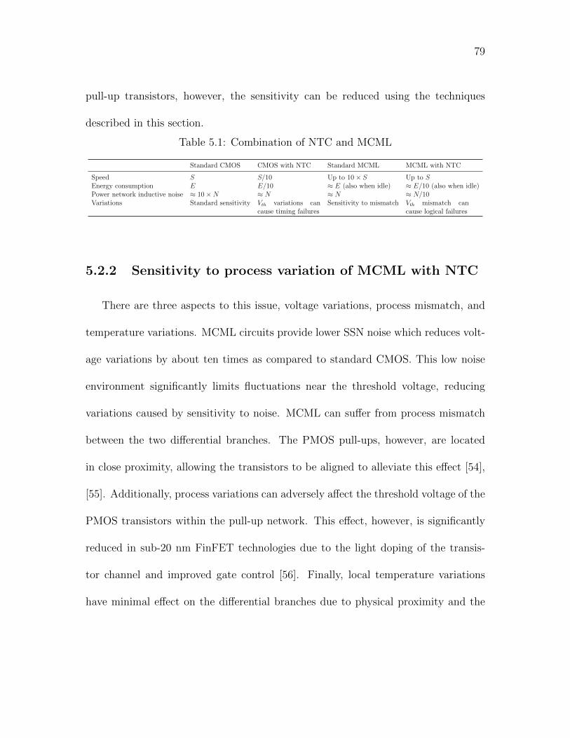
79
pull-up transistors, however, the sensitivity can be reduced using the techniques
described in this section.
Table 5.1: Combination of NTC and MCML
Standard CMOS CMOS with NTC Standard MCML MCML with NTC
Speed S S/10 Up to 10× S Up to SEnergy consumption E E/10 ≈ E (also when idle) ≈ E/10 (also when idle)Power network inductive noise ≈ 10×N ≈ N ≈ N ≈ N/10Variations Standard sensitivity Vth variations can
cause timing failuresSensitivity to mismatch Vth mismatch can
cause logical failures
5.2.2 Sensitivity to process variation of MCML with NTC
There are three aspects to this issue, voltage variations, process mismatch, and
temperature variations. MCML circuits provide lower SSN noise which reduces volt-
age variations by about ten times as compared to standard CMOS. This low noise
environment significantly limits fluctuations near the threshold voltage, reducing
variations caused by sensitivity to noise. MCML can suffer from process mismatch
between the two differential branches. The PMOS pull-ups, however, are located
in close proximity, allowing the transistors to be aligned to alleviate this effect [54],
[55]. Additionally, process variations can adversely affect the threshold voltage of the
PMOS transistors within the pull-up network. This effect, however, is significantly
reduced in sub-20 nm FinFET technologies due to the light doping of the transis-
tor channel and improved gate control [56]. Finally, local temperature variations
have minimal effect on the differential branches due to physical proximity and the
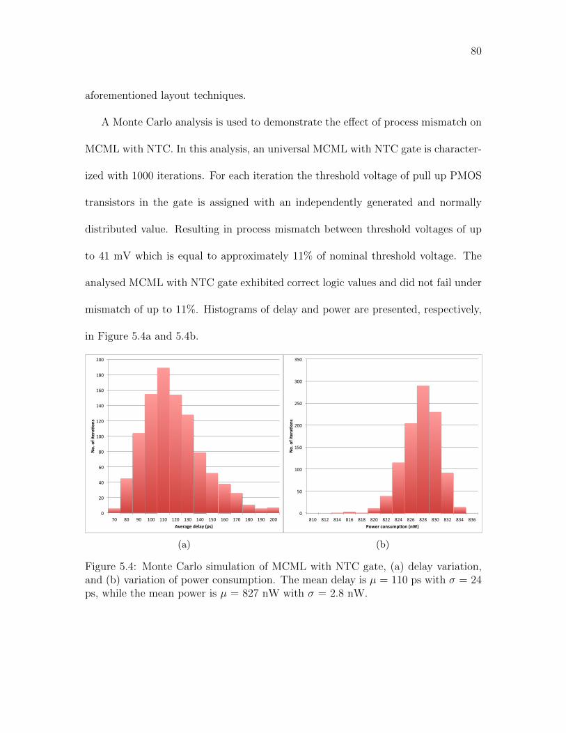
80
aforementioned layout techniques.
A Monte Carlo analysis is used to demonstrate the effect of process mismatch on
MCML with NTC. In this analysis, an universal MCML with NTC gate is character-
ized with 1000 iterations. For each iteration the threshold voltage of pull up PMOS
transistors in the gate is assigned with an independently generated and normally
distributed value. Resulting in process mismatch between threshold voltages of up
to 41 mV which is equal to approximately 11% of nominal threshold voltage. The
analysed MCML with NTC gate exhibited correct logic values and did not fail under
mismatch of up to 11%. Histograms of delay and power are presented, respectively,
in Figure 5.4a and 5.4b.
0
20
40
60
80
100
120
140
160
180
200
70 80 90 100 110 120 130 140 150 160 170 180 190 200
No. of itera+o
ns
Average delay (ps)
(a)
0
50
100
150
200
250
300
350
810 812 814 816 818 820 822 824 826 828 830 832 834 836
No. of itera+o
ns
Power consump+on (nW)
(b)
Figure 5.4: Monte Carlo simulation of MCML with NTC gate, (a) delay variation,and (b) variation of power consumption. The mean delay is µ = 110 ps with σ = 24ps, while the mean power is µ = 827 nW with σ = 2.8 nW.
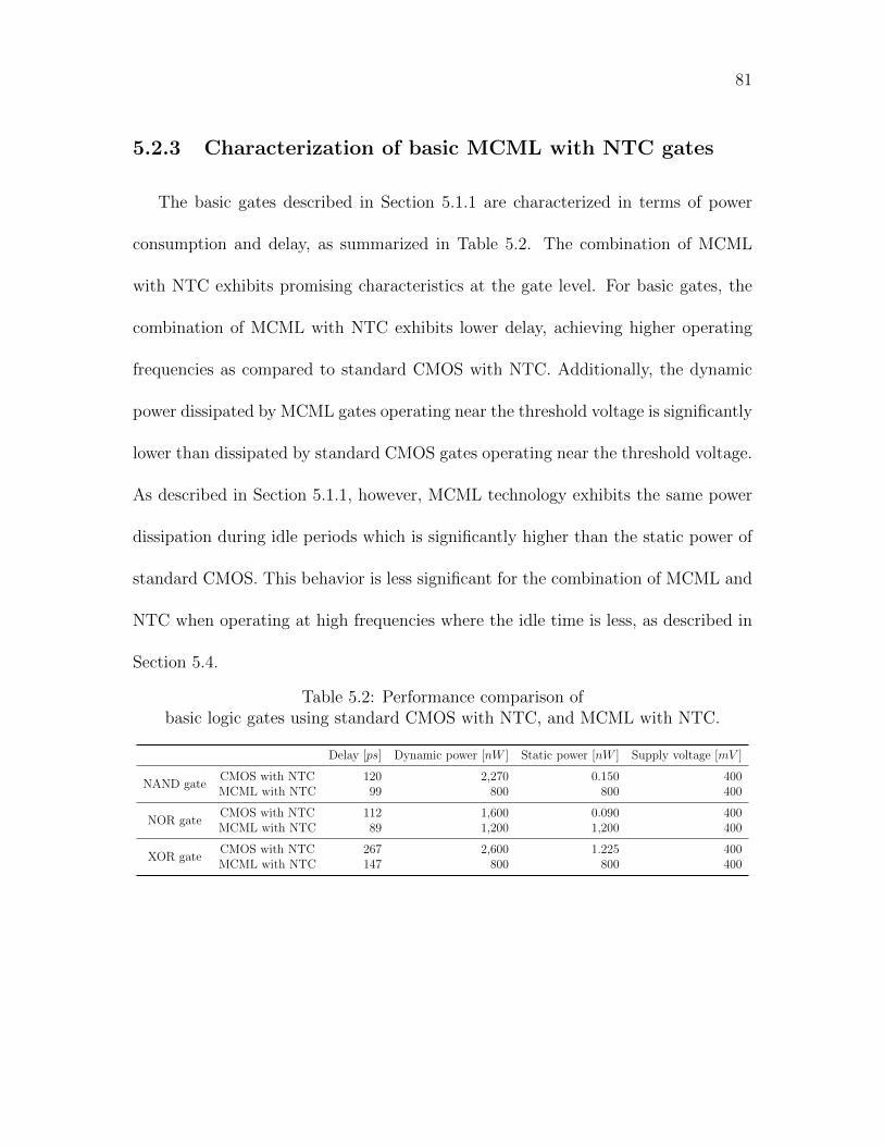
81
5.2.3 Characterization of basic MCML with NTC gates
The basic gates described in Section 5.1.1 are characterized in terms of power
consumption and delay, as summarized in Table 5.2. The combination of MCML
with NTC exhibits promising characteristics at the gate level. For basic gates, the
combination of MCML with NTC exhibits lower delay, achieving higher operating
frequencies as compared to standard CMOS with NTC. Additionally, the dynamic
power dissipated by MCML gates operating near the threshold voltage is significantly
lower than dissipated by standard CMOS gates operating near the threshold voltage.
As described in Section 5.1.1, however, MCML technology exhibits the same power
dissipation during idle periods which is significantly higher than the static power of
standard CMOS. This behavior is less significant for the combination of MCML and
NTC when operating at high frequencies where the idle time is less, as described in
Section 5.4.
Table 5.2: Performance comparison ofbasic logic gates using standard CMOS with NTC, and MCML with NTC.
Delay [ps] Dynamic power [nW ] Static power [nW ] Supply voltage [mV ]
NAND gateCMOS with NTC 120 2,270 0.150 400MCML with NTC 99 800 800 400
NOR gateCMOS with NTC 112 1,600 0.090 400MCML with NTC 89 1,200 1,200 400
XOR gateCMOS with NTC 267 2,600 1.225 400MCML with NTC 147 800 800 400

82
5.3 Simulation setup
In this section, standard CMOS circuits and MCML-based NTC circuits are
compared. The analysis is based on 14 nm low power (LP) FinFET predictive
technology models [35]. A standard threshold voltage of Vth = 350 mV is assumed.
The supply voltage is set to 400 mV to operate near the threshold voltage with
an MCML voltage swing of 100 mV. A Kogge Stone adder is used to evaluate this
proposed circuit topology and is described in Subsection 5.3.1. Power and noise
simulation setups are described, respectively, in Subsections 5.3.2 and 5.3.3.
5.3.1 Description of test circuit
A 32 bit Kogge Stone adder [57] is evaluated in both standard CMOS, and MCML
with NTC. The Kogge Stone adder is a parallel carry look ahead adder [57]. The
choice of a 32 bit Kogge Stone adder as a test circuit is due to the high speed nature
of this circuit topology. The structure of the 32 bit test circuit is demonstrated with
an 8 bit Kogge Stone adder, as presented in Figure 5.5. The 8 bit Kogge Stone
adder has the same periodic structure as the 32 bit adder. The adder is composed
of three building blocks, bit propagate, group generate, and group propagate cells,
with a 32 bit input and 32 bit output. The critical delay path is highlighted in red,
as shown in Figure 5.5. This critical path is used for evaluating the worst case delay
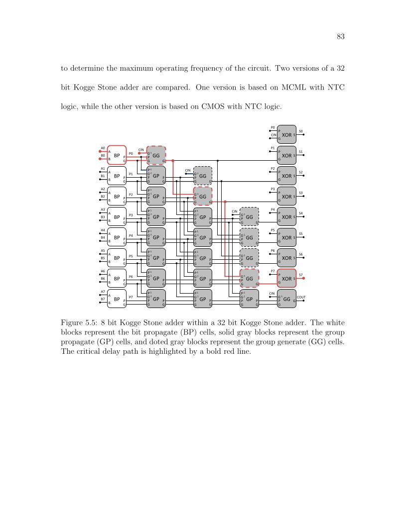
83
to determine the maximum operating frequency of the circuit. Two versions of a 32
bit Kogge Stone adder are compared. One version is based on MCML with NTC
logic, while the other version is based on CMOS with NTC logic.
GG
XOR
BP
GG
GG
G
G-‐1 P G
GP G
G-‐1 P G
P-‐1
P
GP G
G-‐1 P G
P-‐1
P
GP G
G-‐1 P G
P-‐1
P
GP G
G-‐1 P G
P-‐1
P
GP G
G-‐1 P G
P-‐1
P
GP G
G-‐1 P G
P-‐1
P
GP G
G-‐1 P G
P-‐1
P
GP G
G-‐1 P G
P-‐1
P
GP G
G-‐1 P G
P-‐1
P
GP G
G-‐1 P G
P-‐1
P
GP G
G-‐1 P G
P-‐1
P
GP G
G-‐1 P G
P-‐1
P GP G
G-‐1 P G
P-‐1
P GG G G-‐1 P G
XOR S P
G
XOR S P
G
XOR S P
G
XOR S P
G
XOR S P
G
XOR S P
G
XOR S P
G
S P
G
P G
A
B
A0
B0
A1
B1
A2
B2
A3
B3
A4
B4
A5
B5
A6
B6
A7
B7
BP P G
A
B
BP P G
A
B
BP P G
A
B
BP P G
A
B
BP P G
A
B
BP P G
A
B
BP P G
A
B
GG G
G-‐1 P G
G
G-‐1 P G
GG G
G-‐1 P G
G
G-‐1 P G
GG G
G-‐1 P G
GG G
G-‐1 P G
P0
P1
P2
P3
P4
P5
P6
P7
CIN
CIN
CIN
CIN
P0
P1
P2
P3
P4
P5
P6
P7
COUT
S0
S1
S2
S3
S4
S5
S6
S7
CIN
Figure 5.5: 8 bit Kogge Stone adder within a 32 bit Kogge Stone adder. The whiteblocks represent the bit propagate (BP) cells, solid gray blocks represent the grouppropagate (GP) cells, and doted gray blocks represent the group generate (GG) cells.The critical delay path is highlighted by a bold red line.
84
5.3.2 Power simulation setup
The power versus frequency characteristics of the Kogge Stone adder is illustrated
in Figure 5.7. Both MCML and standard CMOS circuits are stimulated with the
same 32 bit input with a duty cycle equivalent to 1 GHz. The input with the longest
propagation delay TD sets the maximum possible operating frequency Fmax = 1/TD
of the circuit. The different power consumption levels are dependent on the supply
voltage for standard CMOS, varying from subthreshold operation (200 mV) to nom-
inal voltage (800 mV). For MCML NTC circuits, however the power consumption is
primarily dependent on the tail current. The power consumption is the average with
different inputs, and consists of both dynamic and static power consumption. The
dynamic power consumption is the average power consumed by the test circuits dur-
ing a signal transition. The static power consumption is the average power consumed
during the remaining portion of the input cycle when the logic is idle. Note that the
static power consumption is a key difference between standard CMOS and MCML
Therefore, to produce a fair comparison, standard CMOS is compared to MCML
with activity factors of 10%, 20%, and 100%. These activity factors represent a wide
range of circuits, from active each cycle (e.g., clock distribution signals) to active
only every tenth cycle (common data paths).
For standard CMOS, frequencies above 9 GHz cannot be achieved with minimum
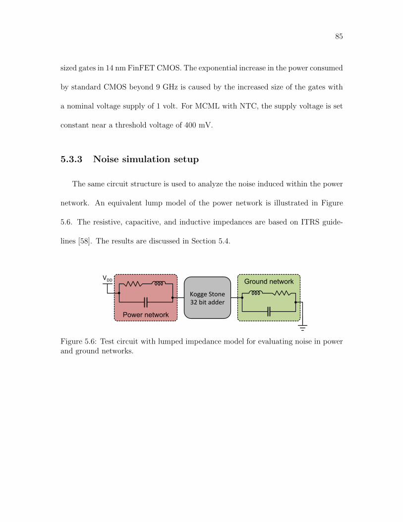
85
sized gates in 14 nm FinFET CMOS. The exponential increase in the power consumed
by standard CMOS beyond 9 GHz is caused by the increased size of the gates with
a nominal voltage supply of 1 volt. For MCML with NTC, the supply voltage is set
constant near a threshold voltage of 400 mV.
5.3.3 Noise simulation setup
The same circuit structure is used to analyze the noise induced within the power
network. An equivalent lump model of the power network is illustrated in Figure
5.6. The resistive, capacitive, and inductive impedances are based on ITRS guide-
lines [58]. The results are discussed in Section 5.4.
Ground network
Power network
Kogge Stone 32 bit adder
VDD
Figure 5.6: Test circuit with lumped impedance model for evaluating noise in powerand ground networks.
86
5.4 Simulation results
The power, speed, and noise characteristics of standard CMOS, and MCML with
NTC are presented in the following subsections.
5.4.1 Power/speed
The power consumed by a 32 bit Kogge Stone adder is shown in Figure 5.7,
as described in Section 5.3. As expected from the gate performance characteristics
listed in Table 5.2, MCML with NTC is more power efficient than standard CMOS
with NTC when operating at high frequencies.
Three speed/power behaviors of interest are exhibited, as illustrated in Figure
5.7. At 1 GHz, the power consumed by MCML with NTC is less than standard
CMOS at a 100% activity factor. In other words, the combination of MCML with
NTC is more power efficient for circuits operating at frequencies above 1 GHz and
switching every cycle. These types of circuits are not limited to clock distribution
networks.
At around 9 GHz, the CMOS circuit reaches the maximum operating frequency
at a nominal supply voltage with minimum sized gates. To further lower the delay
(to increase the frequency), the CMOS gates need to be significantly larger. A sharp
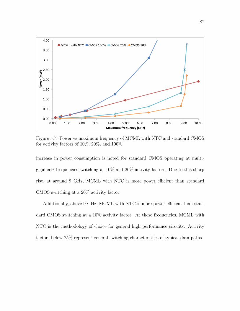
87
0.00
0.50
1.00
1.50
2.00
2.50
3.00
3.50
4.00
0.00 1.00 2.00 3.00 4.00 5.00 6.00 7.00 8.00 9.00 10.00
Power (m
W)
Maximum frequency (GHz)
MCML with NTC CMOS 100% CMOS 20% CMOS 10%
Figure 5.7: Power vs maximum frequency of MCML with NTC and standard CMOSfor activity factors of 10%, 20%, and 100%
increase in power consumption is noted for standard CMOS operating at multi-
gigahertz frequencies switching at 10% and 20% activity factors. Due to this sharp
rise, at around 9 GHz, MCML with NTC is more power efficient than standard
CMOS switching at a 20% activity factor.
Additionally, above 9 GHz, MCML with NTC is more power efficient than stan-
dard CMOS switching at a 10% activity factor. At these frequencies, MCML with
NTC is the methodology of choice for general high performance circuits. Activity
factors below 25% represent general switching characteristics of typical data paths.
88
These characteristics of MCML with NTC position this technology as a signif-
icant competitor to standard CMOS when operating at high activity factors, or
multi-gigahertz frequencies regardless of the activity factor. Unlike standard CMOS,
MCML is capable of power efficient operation at frequencies beyond 9 GHz (in 14
nm technology), enabling power efficient operation at multi-gigahertz frequencies.
5.4.2 Noise
The maximum induced noise in a power network due to switching activity is listed
in Table 5.3. As noted in this table, the SSN in MCML circuits is, on average, an
order of magnitude lower than in static CMOS. The low noise environment is partic-
ularly beneficial for deeply scaled circuits operating near the threshold voltage that
suffer from high sensitivity to process and environment variations. This capability
supports heterogeneous systems that integrate noise sensitive analog circuits with
digital logic and memory. In contrast to standard CMOS circuits with significant
simultaneous switching noise, extensive effort to isolate sensitive circuits from switch-
ing noise is not required in NTC MCML. Additionally, the low noise environment
enables lower noise margins, resulting in more power efficient and/or higher speed
circuits. This low noise characteristic represents a significant advantage of MCML
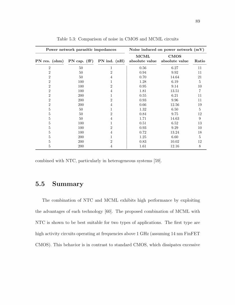
89
Table 5.3: Comparison of noise in CMOS and MCML circuits
Power network parasitic impedances Noise induced on power network (mV)
MCML CMOSPN res. (ohm) PN cap. (fF) PN ind. (nH) absolute value absolute value Ratio
2 50 1 0.56 6.27 112 50 2 0.94 9.92 112 50 4 0.70 14.64 212 100 1 1.28 6.19 52 100 2 0.95 9.14 102 100 4 1.81 13.51 72 200 1 0.55 6.21 112 200 2 0.93 9.96 112 200 4 0.66 12.56 195 50 1 1.32 6.50 55 50 2 0.84 9.75 125 50 4 1.71 14.63 95 100 1 0.51 6.52 135 100 2 0.93 9.29 105 100 4 0.72 13.24 185 200 1 1.25 6.60 55 200 2 0.83 10.02 125 200 4 1.61 12.16 8
combined with NTC, particularly in heterogeneous systems [59].
5.5 Summary
The combination of NTC and MCML exhibits high performance by exploiting
the advantages of each technology [60]. The proposed combination of MCML with
NTC is shown to be best suitable for two types of applications. The first type are
high activity circuits operating at frequencies above 1 GHz (assuming 14 nm FinFET
CMOS). This behavior is in contrast to standard CMOS, which dissipates excessive
90
power at high activity factors. The second type are low activity circuits operating
at frequencies above 9 GHz. At these high frequencies, CMOS is inefficient due to
the linear dependence of dynamic power with frequency. The combination of MCML
with NTC, therefore, provides an effective high performance, power efficient circuit
technology for hight speed and/or high activity applications.
91
Chapter 6
Adaptive power gating applicationof 32-bit adder at 16 nm FinFETtechnology node
Two decades have passed since the concept of power gating was first introduced
[6]. In his work, S. Mutoh et al. utilized low threshold voltage transistors to enhance
the speed of a power gated circuit, while high threshold voltage power gates reduced
the leakage current during a sleep period. Consequently, a number of studies has
been published to address the most common disadvantages of power gating. The
noise voltage induced by the rush current at wakeup has been addressed in [61]
with skewed wakeup timing. Data retention mode operation is presented in [62] to
eliminate information loss. The size of the power gate as a tradeoff between standby
leakage current and speed degradation has been examined in [63]. An automated
gate biasing technique has been developed to determine the gate bias voltage which

92
minimizes leakage current [64]. Power gating characterization at early stages of the
design process has been proposed [65]. Novel power gating approaches that utilize
nano-electro-mechanical power switches with zero leakage current (off state) rather
than MOS power switches have been examined [66]. Application guided power gating
techniques that reduce leakage current in a register file based on the software state
have also been developed [67].
In this chapter an adaptive and independent power gating technique is proposed.
This high granularity local power gating approach lowers overhead and improves ef-
ficiency as compared to global power gating. This technique has been demonstrated
on a 32-bit Kogge Stone adder [57]. The adder is divided into an energy efficient
number of clusters that can be independently powered down when inactive. The
primary contribution of this work is the local controller that enables fine grain power
gating of a clustered circuit by adapting to the current state of the adder. This tech-
nique saves additional power when a circuit is partially active. The nearby location
of the controller also reduces system level complexity such as layout congestion and
sleep/wake up delay, leading to additional power savings.
The chapter is organized as follows. In Section 6.1, the structure of the 32-bit
Kogge Stone adder is reviewed. In Section 6.2, the proposed adaptive power gating
technique is described. Evaluation of the adaptive power gating technique is provided

93
in Section 6.3. The chapter is summarized in Section 6.4.
6.1 32-bit Kogge Stone adder structure
The proposed adaptive power gating technique is evaluated on a 32-bit Kogge
Stone adder [57]. The circuit consists of three major stages; the input, carry prop-
agation network, and output stages. Two one-bit inputs are processed by the input
stage, generating Pi (propagate) and Gi (generate) signals. The propagate signal in-
dicates that the carry signal from the i− 1 bit can propagate through bit i, and the
generate signal indicates that the carry signal is generated at bit i. Both propagate
and generate signals cannot be simultaneously high, and are described by, respec-
tively, (6.1) and (6.2). The carry propagate network is responsible for propagating
the carry signal from the previous bit lines. This carry propagate stage generates
P ∗i and G∗i , given by, respectively, (6.3) and (6.4), which passes the carry signal to
the last output stage. The output stage performs the XOR operation between the
generate signal of the previous bit (Gi−1) and the propagate signal of the current bit
(Pi). The entire structure is illustrated with an 8-bit adder example, as shown in
94
Figure 6.1.
(Ai)XOR(Bi) = Pi (6.1)
(Ai)AND(Bi) = Gi (6.2)
(Pi)AND(Pi−1) = P ∗i (6.3)
(Gi−1)AND(Pi)OR(Gi) = G∗i (6.4)
The adder is logically organized into horizontal clusters of one bit, each comprising
the three major stages, the single bit input, carry propagate network, and output.
Each cluster is independent except for the downstream carry network. Independent
clustering enables the proposed fine grain, adaptive, and local power gating tech-
nique. Furthermore, the clusters can be combined to form up to 32-bit clusters. The
most efficient cluster size is discussed in Section 6.2.4.
6.2 Adaptive power gating of 32-bit Kogge Stone
adder
The proposed adaptive power gating methodology consists of three major com-
ponents: power switches, isolation cells, and a controller, which are described in the
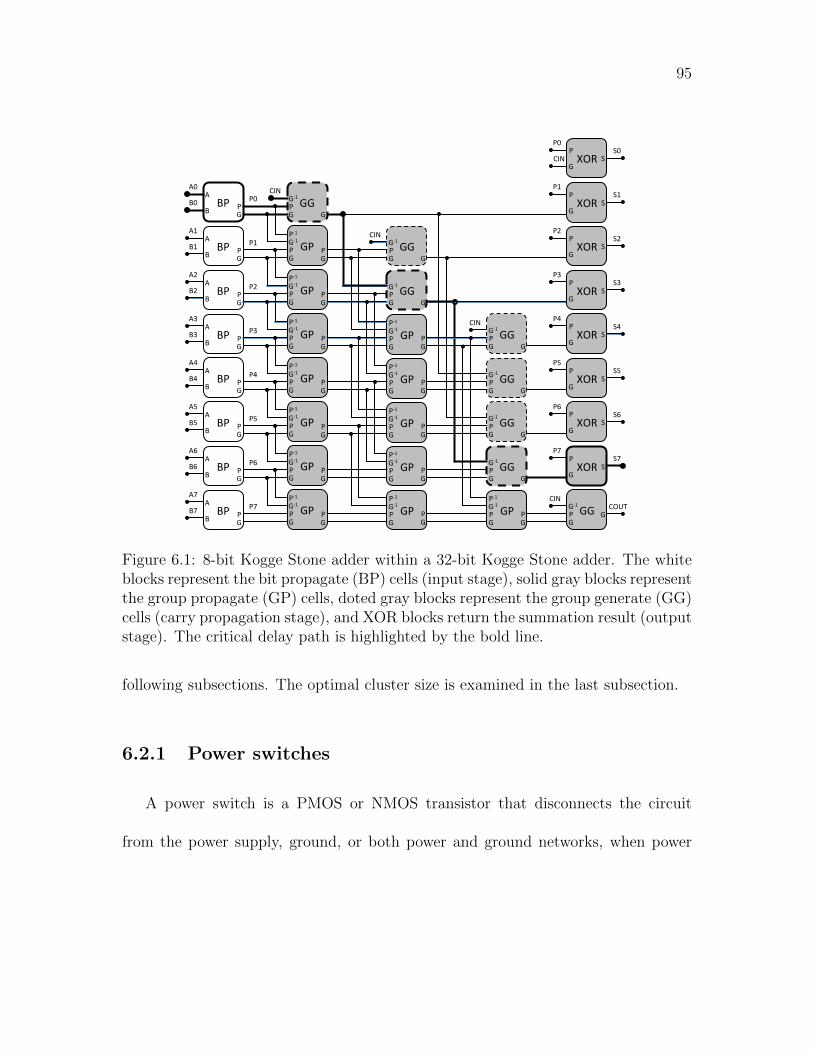
95
GG
XOR
BP
GG
GG
G
G-‐1 P G
GP G
G-‐1 P G
P-‐1
P
GP G
G-‐1 P G
P-‐1
P
GP G
G-‐1 P G
P-‐1
P
GP G
G-‐1 P G
P-‐1
P
GP G
G-‐1 P G
P-‐1
P
GP G
G-‐1 P G
P-‐1
P
GP G
G-‐1 P G
P-‐1
P
GP G
G-‐1 P G
P-‐1
P
GP G
G-‐1 P G
P-‐1
P
GP G
G-‐1 P G
P-‐1
P
GP G
G-‐1 P G
P-‐1
P
GP G
G-‐1 P G
P-‐1
P GP G
G-‐1 P G
P-‐1
P GG G G-‐1 P G
XOR S P
G
XOR S P
G
XOR S P
G
XOR S P
G
XOR S P
G
XOR S P
G
XOR S P
G
S P
G
P G
A
B
A0
B0
A1
B1
A2
B2
A3
B3
A4
B4
A5
B5
A6
B6
A7
B7
BP P G
A
B
BP P G
A
B
BP P G
A
B
BP P G
A
B
BP P G
A
B
BP P G
A
B
BP P G
A
B
GG G
G-‐1 P G
G
G-‐1 P G
GG G
G-‐1 P G
G
G-‐1 P G
GG G
G-‐1 P G
GG G
G-‐1 P G
P0
P1
P2
P3
P4
P5
P6
P7
CIN
CIN
CIN
CIN
P0
P1
P2
P3
P4
P5
P6
P7
COUT
S0
S1
S2
S3
S4
S5
S6
S7
CIN
Figure 6.1: 8-bit Kogge Stone adder within a 32-bit Kogge Stone adder. The whiteblocks represent the bit propagate (BP) cells (input stage), solid gray blocks representthe group propagate (GP) cells, doted gray blocks represent the group generate (GG)cells (carry propagation stage), and XOR blocks return the summation result (outputstage). The critical delay path is highlighted by the bold line.
following subsections. The optimal cluster size is examined in the last subsection.
6.2.1 Power switches
A power switch is a PMOS or NMOS transistor that disconnects the circuit
from the power supply, ground, or both power and ground networks, when power

96
gating is engaged. The addition of the power switches results in a secondary power
network which can be disconnected from the primary power network. This secondary
power network is referred to here as the virtual VDD/Gnd network. Traditionally,
the choice between a footer or header device [26] is based on the circuit structure
and performance tradeoffs. Both footer and header power switches are rarely used
in the same circuit due to the increased delay and area overhead. With FinFET
technology, the performance gap between NMOS and PMOS is less [68], leaving the
choice based solely on the circuit structure. For example, if the VDD supply voltage
is externally gated, a header switch powers down the internal circuit. Alternatively,
if a high voltage is preferred at the outputs of the power gated circuit, disconnecting
the ground with a footer switch is preferable.
In this work, the internal blocks benefit from a low voltage at the outputs of the
power gated block. The power switches therefore use PMOS header transistors. The
low voltage at the outputs, in this configuration, is provided by the isolation cells,
as described in the next subsection.
The length of the power switch (18 nm) is based on the maximum Ion/Ioff ratio
as a function of gate length. The width of the power switch is a function of the size
and peak current of the cluster as well as the number of distributed power switches.
To limit the effect on circuit speed, the width is adjusted until a 10% constraint on
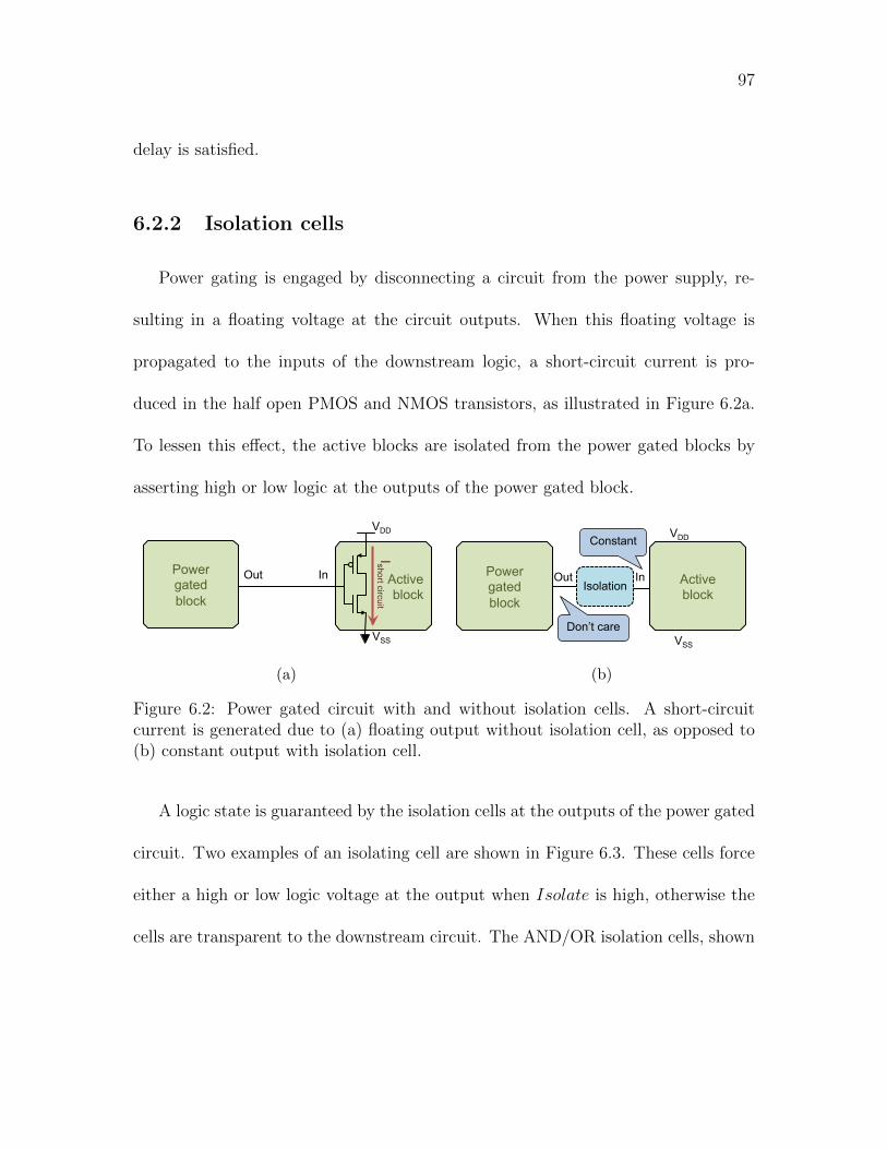
97
delay is satisfied.
6.2.2 Isolation cells
Power gating is engaged by disconnecting a circuit from the power supply, re-
sulting in a floating voltage at the circuit outputs. When this floating voltage is
propagated to the inputs of the downstream logic, a short-circuit current is pro-
duced in the half open PMOS and NMOS transistors, as illustrated in Figure 6.2a.
To lessen this effect, the active blocks are isolated from the power gated blocks by
asserting high or low logic at the outputs of the power gated block.
Power gated block
Out In Active block
VDD
VSS
Ishort circuit
(a)
Power gated block
Active block
VDD
VSS
Out In
Constant
Don’t care
Isolation
(b)
Figure 6.2: Power gated circuit with and without isolation cells. A short-circuitcurrent is generated due to (a) floating output without isolation cell, as opposed to(b) constant output with isolation cell.
A logic state is guaranteed by the isolation cells at the outputs of the power gated
circuit. Two examples of an isolating cell are shown in Figure 6.3. These cells force
either a high or low logic voltage at the output when Isolate is high, otherwise the
cells are transparent to the downstream circuit. The AND/OR isolation cells, shown
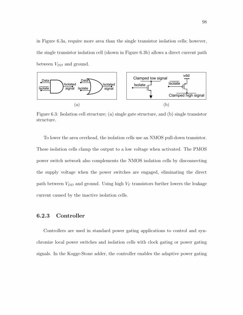
98
in Figure 6.3a, require more area than the single transistor isolation cells; however,
the single transistor isolation cell (shown in Figure 6.3b) allows a direct current path
between VDD and ground.
Data
Isolate Isolated signal
Data
Isolate Isolated signal
(a)
Isolate
Clamped low signal vdd
Isolate
Clamped high signal
(b)
Figure 6.3: Isolation cell structure; (a) single gate structure, and (b) single transistorstructure.
To lower the area overhead, the isolation cells use an NMOS pull-down transistor.
These isolation cells clamp the output to a low voltage when activated. The PMOS
power switch network also complements the NMOS isolation cells by disconnecting
the supply voltage when the power switches are engaged, eliminating the direct
path between VDD and ground. Using high VT transistors further lowers the leakage
current caused by the inactive isolation cells.
6.2.3 Controller
Controllers are used in standard power gating applications to control and syn-
chronize local power switches and isolation cells with clock gating or power gating
signals. In the Kogge-Stone adder, the controller enables the adaptive power gating

99
scheme. Two controller configurations are used to adapt to a specific input scenario
of the 32-bit Kogge Stone adder. A simple controller and an enhanced controller are
discussed in this section.
6.2.3.1 Simple adaptive controller
As described in Section 6.1, the carry propagate stage of the adder is responsible
for a significant fraction of the area and energy consumption of an adder. This carry
propagation network, however, is redundant for bit i when both input bits, Ai and
Bi, are zero. The simple adaptive controller recognizes this specific input pattern
and applies power gating to the corresponding carry network. In the case of clusters
larger than a single bit size, as exemplified by the 4-bit clusters shown in Figure
6.4, the controller considers four bits of the corresponding inputs. In this case, the
controller implements a boolean function, (Ai+Bi+A(i+1)+B(i+1)+A(i+2)+B(i+2)+
A(i+3) + B(i+3))′ to recognize the four consecutive zero input bits. The controller
dynamically power gates only those circuits that are part of the carry propagation
network. The power gated circuits, as illustrated in Figure 6.4, are highlighted in
gray and are isolated from the active output stage (highlighted by the black diagonal
stripes) using isolation units (black/white diamonds). The input stage (highlighted
in white) and the output stage are maintained active to guarantee correct operation
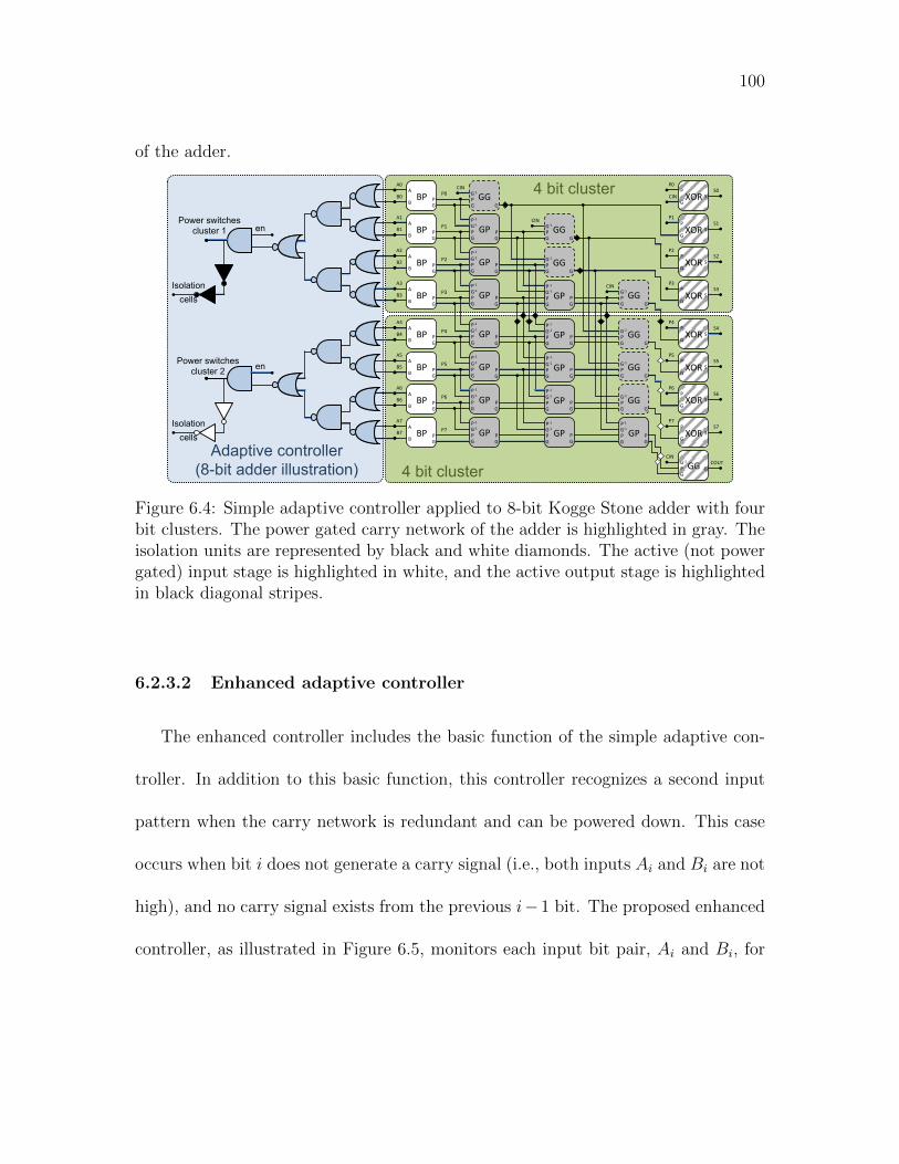
100
of the adder.
GG G
G-‐1 P G
GP G
G-‐1 P G
P-‐1
P
GP G
G-‐1 P G
P-‐1
P
GP G
G-‐1 P G
P-‐1
P
GP G
G-‐1 P G
P-‐1
P
GP G
G-‐1 P G
P-‐1
P
GP G
G-‐1 P G
P-‐1
P
GP G
G-‐1 P G
P-‐1
P
GP G
G-‐1 P G
P-‐1
P
GP G
G-‐1 P G
P-‐1
P
GP G
G-‐1 P G
P-‐1
P
GP G
G-‐1 P G
P-‐1
P
GP G
G-‐1 P G
P-‐1
P GP G
G-‐1 P G
P-‐1
P
GG G G-‐1 P G
XOR S P
G
XOR S P
G
XOR S P
G
XOR S P
G
XOR S P
G
XOR S P
G
XOR S P
G
XOR S P
G
BP P G
A
B
A0
B0
A1
B1
A2
B2
A3
B3
A4
B4
A5
B5
A6
B6
A7
B7
BP P G
A
B
BP P G
A
B
BP P G
A
B
BP P G
A
B
BP P G
A
B
BP P G
A
B
BP P G
A
B
GG G
G-‐1 P G
GG G
G-‐1 P G
GG G
G-‐1 P G
GG G
G-‐1 P G
GG G
G-‐1 P G
GG G
G-‐1 P G
P0
P1
P2
P3
P4
P5
P6
P7
CIN
CIN
CIN
CIN
P0
P1
P2
P3
P4
P5
P6
P7
COUT
S0
S1
S2
S3
S4
S5
S6
S7
CIN 4 bit cluster
4 bit cluster
Power switches cluster 1
Adaptive controller (8-bit adder illustration)
Isolation
cells
en
Power switches cluster 2
Isolation
cells
en
Figure 6.4: Simple adaptive controller applied to 8-bit Kogge Stone adder with fourbit clusters. The power gated carry network of the adder is highlighted in gray. Theisolation units are represented by black and white diamonds. The active (not powergated) input stage is highlighted in white, and the active output stage is highlightedin black diagonal stripes.
6.2.3.2 Enhanced adaptive controller
The enhanced controller includes the basic function of the simple adaptive con-
troller. In addition to this basic function, this controller recognizes a second input
pattern when the carry network is redundant and can be powered down. This case
occurs when bit i does not generate a carry signal (i.e., both inputs Ai and Bi are not
high), and no carry signal exists from the previous i− 1 bit. The proposed enhanced
controller, as illustrated in Figure 6.5, monitors each input bit pair, Ai and Bi, for

101
the occurrence of two input patterns (when the carry network is redundant) based
on the Boolean functions described by (6.5) and (6.6),
G0 + P0 × Cin = CR0 (6.5)
Gi + Pi × CRi−1 = CRi. (6.6)
The primary benefit of this enhanced controller is the significantly expanded pool
of input patterns that becomes available for power gating (not limited to a zero input
as with the simple adaptive controller). A daisy chain connection between bit lines
in the controller is however required, as highlighted by the dotted lines shown in
Figure 6.5. Due to this long chain, the power gating signal from the controller to
the power switches is delayed for most of the significant bits of the adder, leaving a
smaller fraction of the clock period to save static power. Moreover, the daisy chain
can lead to redundant logic switches inside the controller, further reducing energy
efficiency.
6.2.4 Optimal cluster size with shared power switches
The proposed power gating circuit with the simple adaptive controller has been
evaluated to determine the preferable clustering size. The gates within a single
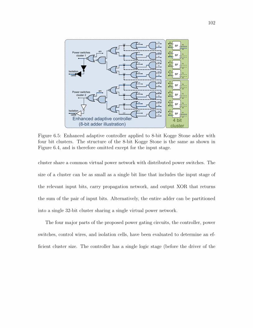
102
Enhanced adaptive controller (8-bit adder illustration)
P0
G0 A0
B0
A1
B1
A2
B2
A3
B3
A4
B4
A5
B5
A6
B6
A7
B7
P0
P1
P2
P3
P4
P5
P6
P7
4 bit cluster
G0
G1
G2
G3
G4
G5
G6
G7
CR0 Cin
P1
G1 CR1
CR0
P2
G2 CR2
P3
G3 CR3
CR2
CR1
P4
G4 CR4
P5
G5 CR5
CR4
P6
G6 CR6
P7
G7 CR7
CR6
CR5
CR3
en Power switches cluster 1
Isolation
cells
en Power switches cluster 2
Isolation
cells
BP P G
A
B
BP P G
A
B
BP P G
A
B
BP P G
A
B
BP P G
A
B
BP P G
A
B
BP P G
A
B
BP P G
A
B
Figure 6.5: Enhanced adaptive controller applied to 8-bit Kogge Stone adder withfour bit clusters. The structure of the 8-bit Kogge Stone is the same as shown inFigure 6.4, and is therefore omitted except for the input stage.
cluster share a common virtual power network with distributed power switches. The
size of a cluster can be as small as a single bit line that includes the input stage of
the relevant input bits, carry propagation network, and output XOR that returns
the sum of the pair of input bits. Alternatively, the entire adder can be partitioned
into a single 32-bit cluster sharing a single virtual power network.
The four major parts of the proposed power gating circuits, the controller, power
switches, control wires, and isolation cells, have been evaluated to determine an ef-
ficient cluster size. The controller has a single logic stage (before the driver of the
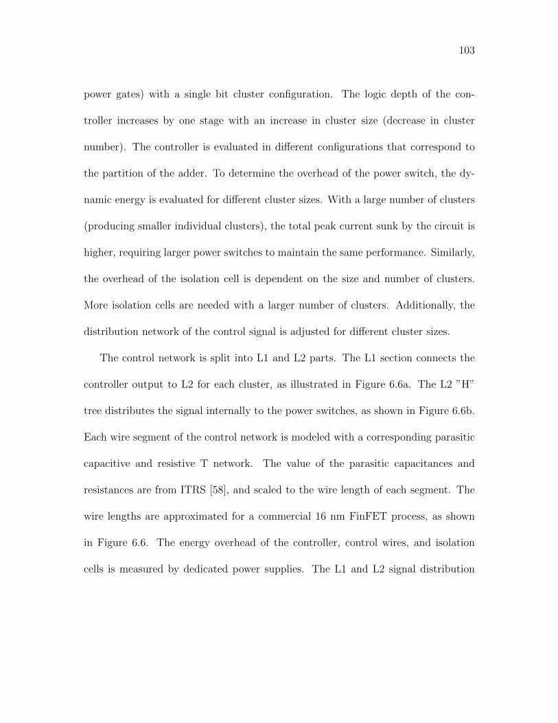
103
power gates) with a single bit cluster configuration. The logic depth of the con-
troller increases by one stage with an increase in cluster size (decrease in cluster
number). The controller is evaluated in different configurations that correspond to
the partition of the adder. To determine the overhead of the power switch, the dy-
namic energy is evaluated for different cluster sizes. With a large number of clusters
(producing smaller individual clusters), the total peak current sunk by the circuit is
higher, requiring larger power switches to maintain the same performance. Similarly,
the overhead of the isolation cell is dependent on the size and number of clusters.
More isolation cells are needed with a larger number of clusters. Additionally, the
distribution network of the control signal is adjusted for different cluster sizes.
The control network is split into L1 and L2 parts. The L1 section connects the
controller output to L2 for each cluster, as illustrated in Figure 6.6a. The L2 ”H”
tree distributes the signal internally to the power switches, as shown in Figure 6.6b.
Each wire segment of the control network is modeled with a corresponding parasitic
capacitive and resistive T network. The value of the parasitic capacitances and
resistances are from ITRS [58], and scaled to the wire length of each segment. The
wire lengths are approximated for a commercial 16 nm FinFET process, as shown
in Figure 6.6. The energy overhead of the controller, control wires, and isolation
cells is measured by dedicated power supplies. The L1 and L2 signal distribution
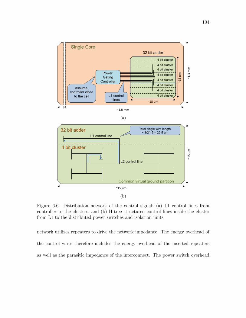
104
Single Core
~1.3 m
m
~1.8 mm
4 bit cluster
4 bit cluster
32 bit adder
L1 control lines
~15 um
~15 um
Assume controller close
to the cell
4 bit cluster
4 bit cluster
4 bit cluster
4 bit cluster
4 bit cluster
4 bit cluster
Power Gating
Controller
(a)
32 bit adder
~15 um
~15 um
4 bit cluster
L1 control line
Common virtual ground partition
Total single wire length ~ 3/2*15 = 22.5 um
L2 control line
(b)
Figure 6.6: Distribution network of the control signal; (a) L1 control lines fromcontroller to the clusters, and (b) H-tree structured control lines inside the clusterfrom L1 to the distributed power switches and isolation units.
network utilizes repeaters to drive the network impedance. The energy overhead of
the control wires therefore includes the energy overhead of the inserted repeaters
as well as the parasitic impedance of the interconnect. The power switch overhead
105
includes the energy of the switching gate capacitance of the power gates.
The results of this analysis are presented in Figure 6.7. As illustrated in Figure
6.7a, the 4-, 8-, and 16-bit clusters exhibit the highest energy efficiency. A higher
energy overhead is reported for both the smaller and larger clusters. As illustrated
in Figure 6.7b, for the smaller clusters, the overhead is due to the inefficient control
network and greater number of isolation units. For the larger clusters, the overhead
is due to the larger controller as well as the sub-optimal control network. The
smallest, yet energy efficient cluster size of four bits is therefore used to exploit
greater granularity without compromising energy efficiency.
6.3 Evaluation and results
Application of the proposed power gating technique to a 32-bit Kogge Stone adder
with 4-bit clusters is evaluated using 16 nm FinFET PTM models [35]. Both of the
controller configurations, simple and enhanced controllers, are compared to a non-
power gated version of the adder. The reported energy consumption of the power
gated circuit includes the overhead of all of the power gating components described
in Section 6.2.
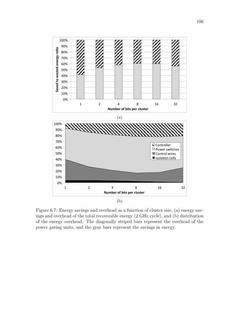
106
0%
10%
20%
30%
40%
50%
60%
70%
80%
90%
100%
1 2 4 8 16 32
Saved to wasted en
ergy ra
/o
Number of bits per cluster
(a)
0%
10%
20%
30%
40%
50%
60%
70%
80%
90%
100%
1 2 4 8 16 32 Number of bits per cluster
Controller Power switches Control wires Isola<on cells
(b)
Figure 6.7: Energy savings and overhead as a function of cluster size, (a) energy sav-ings and overhead of the total recoverable energy (2 GHz cycle), and (b) distributionof the energy overhead. The diagonally striped bars represent the overhead of thepower gating units, and the gray bars represent the savings in energy.
107
6.3.1 Simple adaptive controller
The circuits are injected with a randomly generated input pattern during the
initial 2 GHz clock period followed by a new randomly generated input pattern
during the following clock period. The second input pattern, however, is modified
to include a different number of 4-bit zero groups starting from the most significant
bit (MSB). The simulation is averaged over ten iterations for each number of 4-bit
zero groups of the second input, as depicted in Figure 6.8. This analysis is used to
evaluate the possible energy savings of the proposed fine grain power gating approach
when the 32-bit input operands of the adder contain unused higher order bits. A
sample analysis (which does not include the adder circuit) is performed to provide
insight into the probability of the target input patterns. In this analysis, eight
industry standard software benchmarks (eembc, coremark, linpack, octane, ragdoll,
spec2006, spec2000, and sunspider) are executed on a commercial microprocessor
to simulate general software activity. The number of leading zero bytes within the
input variables to the arithmetic unit in the microprocessor is determined during
the execution. This sample analysis demonstrates that for the majority of inputs
to the adder (on average, 62%) at least one significant byte is equal to zero (two
4-bit clusters can be power gated, saving up to 12% energy). For 30% of the input
patterns, the three most significant bytes are equal to zero (six 4-bit clusters can be
108
power gated, saving up to 19% energy).
The energy is measured during the second cycle by evaluating the integral of the
instantaneous power over the entire cycle. The delay is measured at the 50%-to-50%
transitions at the output. An increase in energy savings of up to 21% is illustrated in
Figure 6.8a. The power gated circuit is 8% more energy efficient when fully active due
to the power switches that limit the dynamic and static power dissipation, trading
off longer delay. The reduced power consumption is primarily due to the additional
resistance (of the power gate) added between the power and ground networks, as well
as the reduced voltage swing across the active circuit due to the voltage drop across
the power gate. Alternatively, the power gated circuit exhibits up to 21% savings
in energy when all of the eight clusters are powered down. Note that the energy
consumption, both for the power gated and non-power gated circuits, declines with
increasing number of powered down clusters. This behavior is expected due to the
lower activity of the adder with the larger number of 4-bit zero groups in the inputs.
The primary tradeoff of applying power gating is delay overhead, as illustrated
in Figure 6.8b. As shown in Figure 6.8b, the delay overhead is, on average, 12% and
does not vary significantly as a function of the number of powered off clusters. This
result agrees with the expected 10% overhead, as described in Section 6.2.1.
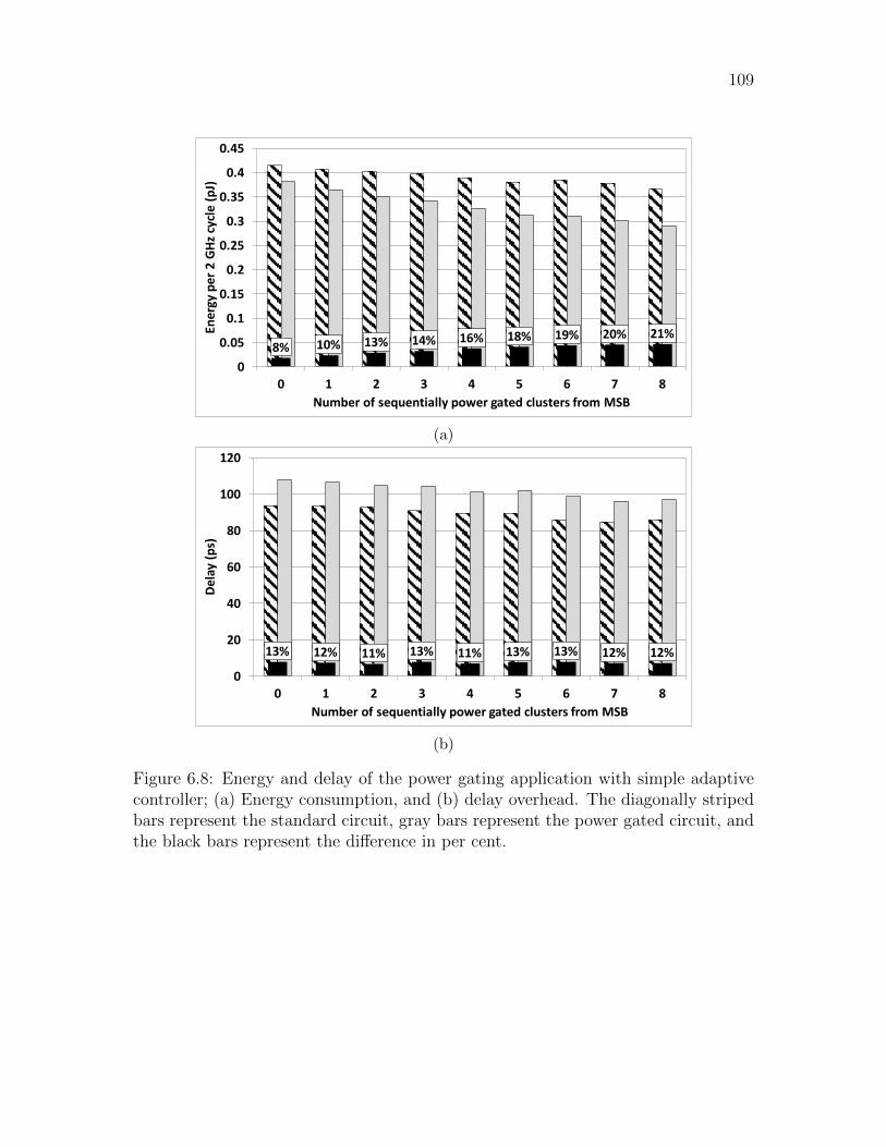
109
8% 10% 13% 14% 16% 18% 19% 20% 21%
0
0.05
0.1
0.15
0.2
0.25
0.3
0.35
0.4
0.45
0 1 2 3 4 5 6 7 8
Energyper2GHz
cycle(pJ)
NumberofsequentiallypowergatedclustersfromMSB
(a)
13% 12% 11% 13% 11% 13% 13% 12% 12%
0
20
40
60
80
100
120
0 1 2 3 4 5 6 7 8
Delay(ps)
NumberofsequentiallypowergatedclustersfromMSB
(b)
Figure 6.8: Energy and delay of the power gating application with simple adaptivecontroller; (a) Energy consumption, and (b) delay overhead. The diagonally stripedbars represent the standard circuit, gray bars represent the power gated circuit, andthe black bars represent the difference in per cent.

110
6.3.2 Comparison of the simple adaptive power gating tech-
nique to standard power gating approach
The simple adaptive power gating technique differs from standard power gating
due to the dedicated controller and additional isolation units. Both techniques share
the same underlying network of power gates and control lines. This network of
power gates, as described in Section 6.2.1, is the primary contributor to the delay
overhead of the power gated circuit. The delay overhead of the power gated circuit is,
however, a function of the size of the power gates which should be optimized for each
power gated circuit based on local speed/area constraints. A dedicated controller,
therefore, does not contribute additional delay since the controller operates parallel
to the adder. Moreover, the additional isolation units contribute an insignificant
delay with a similar contribution both to the standard power gating and simple
adaptive power gating approaches.
The energy overhead, however, is higher in simple adaptive power gating but
the contribution due to the controller and the additional isolation cells is low. The
deleterious effect on the energy savings can be noted in the two extrema cases, as
shown in Figure 6.9.
In the first case, the entire adder is power gated (the right most column in Figure
6.9). The simple adaptive controller is redundant, wasting energy as compared to
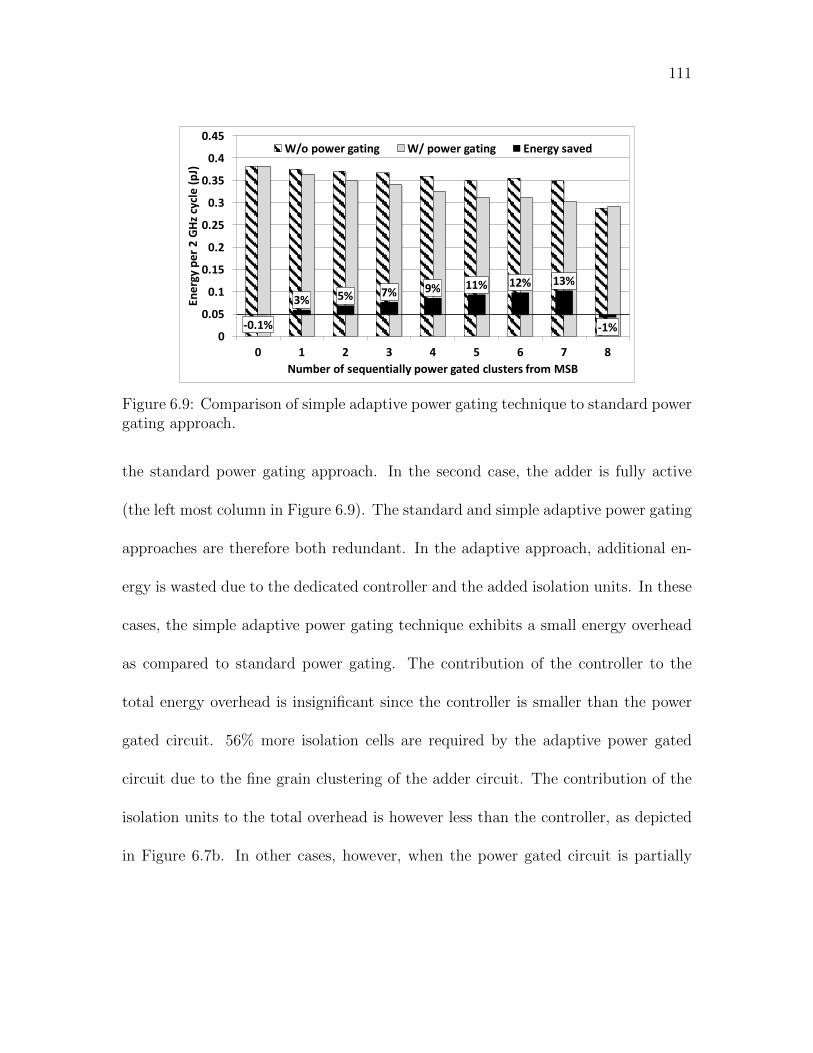
111
-0.1%
3% 5% 7% 9% 11% 12% 13%
-1%0
0.05
0.1
0.15
0.2
0.25
0.3
0.35
0.4
0.45
0 1 2 3 4 5 6 7 8
Energyper2GHz
cycle(pJ)
NumberofsequentiallypowergatedclustersfromMSB
W/opowergating W/powergating Energysaved
Figure 6.9: Comparison of simple adaptive power gating technique to standard powergating approach.
the standard power gating approach. In the second case, the adder is fully active
(the left most column in Figure 6.9). The standard and simple adaptive power gating
approaches are therefore both redundant. In the adaptive approach, additional en-
ergy is wasted due to the dedicated controller and the added isolation units. In these
cases, the simple adaptive power gating technique exhibits a small energy overhead
as compared to standard power gating. The contribution of the controller to the
total energy overhead is insignificant since the controller is smaller than the power
gated circuit. 56% more isolation cells are required by the adaptive power gated
circuit due to the fine grain clustering of the adder circuit. The contribution of the
isolation units to the total overhead is however less than the controller, as depicted
in Figure 6.7b. In other cases, however, when the power gated circuit is partially
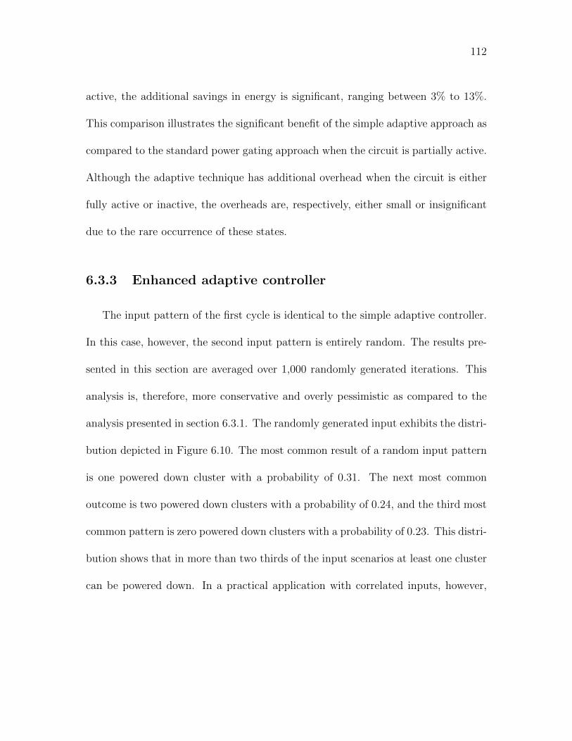
112
active, the additional savings in energy is significant, ranging between 3% to 13%.
This comparison illustrates the significant benefit of the simple adaptive approach as
compared to the standard power gating approach when the circuit is partially active.
Although the adaptive technique has additional overhead when the circuit is either
fully active or inactive, the overheads are, respectively, either small or insignificant
due to the rare occurrence of these states.
6.3.3 Enhanced adaptive controller
The input pattern of the first cycle is identical to the simple adaptive controller.
In this case, however, the second input pattern is entirely random. The results pre-
sented in this section are averaged over 1,000 randomly generated iterations. This
analysis is, therefore, more conservative and overly pessimistic as compared to the
analysis presented in section 6.3.1. The randomly generated input exhibits the distri-
bution depicted in Figure 6.10. The most common result of a random input pattern
is one powered down cluster with a probability of 0.31. The next most common
outcome is two powered down clusters with a probability of 0.24, and the third most
common pattern is zero powered down clusters with a probability of 0.23. This distri-
bution shows that in more than two thirds of the input scenarios at least one cluster
can be powered down. In a practical application with correlated inputs, however,
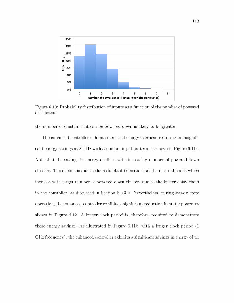
113
0%
5%
10%
15%
20%
25%
30%
35%
0 1 2 3 4 5 6 7 8
Prob
ability
Number of power gated clusters (four bits per cluster)
Figure 6.10: Probability distribution of inputs as a function of the number of poweredoff clusters.
the number of clusters that can be powered down is likely to be greater.
The enhanced controller exhibits increased energy overhead resulting in insignifi-
cant energy savings at 2 GHz with a random input pattern, as shown in Figure 6.11a.
Note that the savings in energy declines with increasing number of powered down
clusters. The decline is due to the redundant transitions at the internal nodes which
increase with larger number of powered down clusters due to the longer daisy chain
in the controller, as discussed in Section 6.2.3.2. Nevertheless, during steady state
operation, the enhanced controller exhibits a significant reduction in static power, as
shown in Figure 6.12. A longer clock period is, therefore, required to demonstrate
these energy savings. As illustrated in Figure 6.11b, with a longer clock period (1
GHz frequency), the enhanced controller exhibits a significant savings in energy of up
114
5.2% 4.6% 4.0% 3.6% 3.0% 2.3% 0.9% 0.1% 0
50
100
150
200
250
300
350
400
450
0 1 2 3 4 5 6 7
Energy per 2 GHz
cycle (p
J)
Number of power gated clusters (four bits per cluster)
(a)
6% 8% 9% 12% 13% 15% 14% 14%
0
100
200
300
400
500
600
700
0 1 2 3 4 5 6 7
Energy per 1 GHz
cycle (p
J)
Number of power gated clusters (four bits per cluster)
(b)
Figure 6.11: Energy consumption of power gating application with enhanced adap-tive controller at (a) 2 GHz clock frequency, and (b) 1 GHz clock frequency. Thediagonally striped bars represent the standard circuit, gray bars represent the powergated circuit, and the black bars represent the difference in per cent.
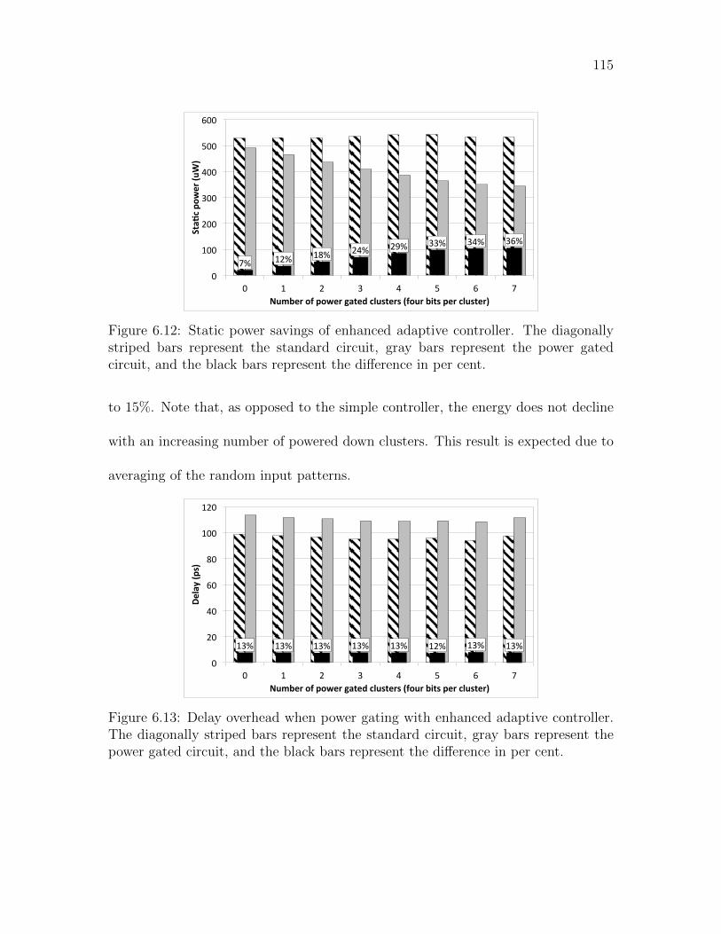
115
7% 12% 18% 24% 29% 33% 34% 36%
0
100
200
300
400
500
600
0 1 2 3 4 5 6 7
Sta$
c po
wer (u
W)
Number of power gated clusters (four bits per cluster)
Figure 6.12: Static power savings of enhanced adaptive controller. The diagonallystriped bars represent the standard circuit, gray bars represent the power gatedcircuit, and the black bars represent the difference in per cent.
to 15%. Note that, as opposed to the simple controller, the energy does not decline
with an increasing number of powered down clusters. This result is expected due to
averaging of the random input patterns.
13% 13% 13% 13% 13% 12% 13% 13%
0
20
40
60
80
100
120
0 1 2 3 4 5 6 7
Delay (ps)
Number of power gated clusters (four bits per cluster)
Figure 6.13: Delay overhead when power gating with enhanced adaptive controller.The diagonally striped bars represent the standard circuit, gray bars represent thepower gated circuit, and the black bars represent the difference in per cent.
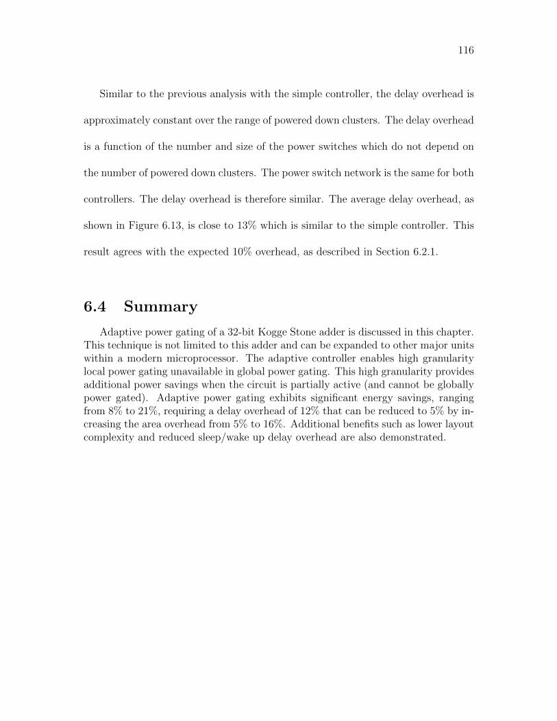
116
Similar to the previous analysis with the simple controller, the delay overhead is
approximately constant over the range of powered down clusters. The delay overhead
is a function of the number and size of the power switches which do not depend on
the number of powered down clusters. The power switch network is the same for both
controllers. The delay overhead is therefore similar. The average delay overhead, as
shown in Figure 6.13, is close to 13% which is similar to the simple controller. This
result agrees with the expected 10% overhead, as described in Section 6.2.1.
6.4 Summary
Adaptive power gating of a 32-bit Kogge Stone adder is discussed in this chapter.This technique is not limited to this adder and can be expanded to other major unitswithin a modern microprocessor. The adaptive controller enables high granularitylocal power gating unavailable in global power gating. This high granularity providesadditional power savings when the circuit is partially active (and cannot be globallypower gated). Adaptive power gating exhibits significant energy savings, rangingfrom 8% to 21%, requiring a delay overhead of 12% that can be reduced to 5% by in-creasing the area overhead from 5% to 16%. Additional benefits such as lower layoutcomplexity and reduced sleep/wake up delay overhead are also demonstrated.
117
Chapter 7
Conclusions
The thirst for knowledge, on demand access to information, and the desire to
solve complex problems have led humanity to the remarkable pace of technological
advancements in the information age. A few decades ago an integrated circuit, the
cornerstone of this progress, consisted of hundreds of discrete components. The com-
plexity of an integrated circuit can now be compared to the complexity of the largest
metropolises of the world shrunk down to the size of a nickel. This complexity is
the result of scaling the transistor dimensions, threshold voltages, channel lengths,
and gate oxide thicknesses to enhance speed, and reduce area and power. Although
scaling has enabled these benefits, from the perspective of the entire microprocessor,
circuits developed in sub-65 nm technology nodes have led to severe power den-
sity issues, rendering conventional heat removal practices impractical. This process
has eventually led to the saturation of processor speeds and greater partitioning of

118
power down circuits, also known as ”dark silicon.” Moreover, the recent shift in fo-
cus to mobile platforms has emphasized energy efficiency in modern battery powered
microprocessors (as compared to power density). As a result, standard techniques
to reduce dynamic and static power consumption are struggling to provide desired
power savings. Techniques such as on-chip dynamic voltage and frequency scaling,
power gating, and many-core systems are being replaced by advanced techniques
that emphasize energy savings. In this dissertation, novel low power circuits and
design techniques have been proposed to enable the greater power savings required
in modern applications.
Supply voltage reductions down to near threshold voltage levels and below is an
attractive methodology to lower dynamic power consumption. A key component
that enables communication among circuits operating at near and sub-threshold
voltages and other voltage levels is a level shifter which translates low voltage digital
signals to higher voltages (and vice versa). A high speed and power efficient level
shifter has been developed to enable communication among multi-voltage domains.
The proposed level shifter enables the extreme voltage scaling required to extract
greater energy savings. Communication between circuits operating near the threshold
voltage and circuits operating at higher voltages is supported. Existing level shifters
are also compared to the proposed circuit, which exhibits significantly shorter delay,
119
lower energy consumption, and less static power dissipation.
A general and important drawback of reducing the supply voltage is the lower
operating speed of the circuit. This compromise in speed can however be mitigated
by exploiting the high performance exhibited by MOS current mode logic (MCML).
This logic style is based on a differential gate structure that trades off high speed
with higher power consumption when idle. The proposed combination of MCML
with NTC, therefore, benefits from the advantages of each technology and is shown
to be best suited for two types of applications. The first type is high activity circuits
operating at frequencies above a gigahertz (assuming 14 nm FinFET CMOS). This
behavior is in contrast to standard CMOS, which dissipates excessive power when
circuits operate at high activity factors. The second type is low activity circuits
operating at frequencies above 9 GHz. At these high frequencies, CMOS is inefficient
due to the linear dependence of dynamic power with frequency. The combination
of MCML with NTC provides an effective high performance, power efficient circuit
technology for high speed and/or high activity applications. Overall, this circuit is
shown to benefit many-core systems that operate at high frequencies and process
highly parallel workloads. A microprocessor architecture utilizing MCML with NTC
circuits technology is evaluated in [69].

120
Addressing dynamic power consumption is not sufficient in sub-30 nm technolo-
gies. Static power consumption can overshadow dynamic power in deeply scaled
circuits. Techniques to lower leakage power have therefore become an important ob-
jective in modern microprocessors. To address this issue, an adaptive power gating
technique is proposed. This power gating technique utilizes a high level of gran-
ularity to save additional leakage power when the circuit is active as opposed to
standard power gating that saves static power only when the entire circuit is pow-
ered off. To enable this behavior, an adaptive controller is proposed that disables
unused partitions within a Kogge-Stone adder by examining the input to the adder.
This technique is shown to provide significant savings in static power in addition to
the standard benefits of reduced dynamic power derived from classical power gating.
Optimizing the wide supply voltage range of signals propagating across long inter-
connect enables greater energy savings from aggressive voltage scaling. The primary
contribution is optimization of the repeater insertion process for wide supply volt-
age range applications. A closed-form sub-22 nm FinFET delay model supporting
a wide voltage range is developed to enable this capability. The model supports
an ultra-wide voltage range from nominal voltages to sub-threshold voltage levels,
and a wide range of repeater sizes. The model is validated with SPICE, exhibiting
accuracy across the entire parameter space. Challenges to repeater insertion are also

121
addressed and evaluated using the proposed model.
To conclude, the classic solutions that reduce power consumption in high perfor-
mance integrated circuits struggle to provide the desired energy efficiency in modern
microprocessors and emerging mobile platforms. By examining the weaknesses of
these classic solutions, novel and enhanced power reduction techniques are proposed
in this dissertation to address the primary power consumption mechanisms. Improve-
ments in energy efficiency are enabled by reducing both static and dynamic power
consumption utilizing adaptive and near threshold circuit techniques. These ad-
vanced power reduction techniques will enable the greater energy efficiency required
in modern portable systems.
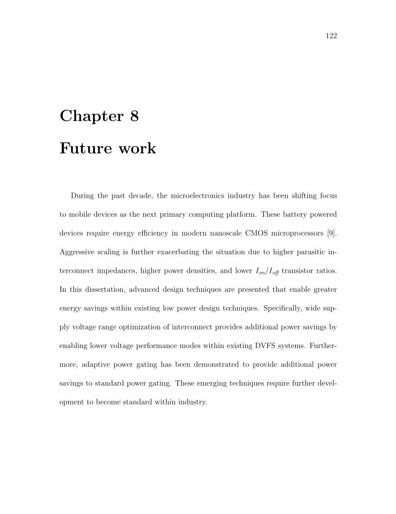
122
Chapter 8
Future work
During the past decade, the microelectronics industry has been shifting focus
to mobile devices as the next primary computing platform. These battery powered
devices require energy efficiency in modern nanoscale CMOS microprocessors [9].
Aggressive scaling is further exacerbating the situation due to higher parasitic in-
terconnect impedances, higher power densities, and lower Ion/Ioff transistor ratios.
In this dissertation, advanced design techniques are presented that enable greater
energy savings within existing low power design techniques. Specifically, wide sup-
ply voltage range optimization of interconnect provides additional power savings by
enabling lower voltage performance modes within existing DVFS systems. Further-
more, adaptive power gating has been demonstrated to provide additional power
savings to standard power gating. These emerging techniques require further devel-
opment to become standard within industry.
123
8.1 Power Centric Interconnect Optimization for
Wide Supply Voltage Applications
A closed-form delay model of interconnect with inserted repeaters that supports a
wide supply voltage range in sub-22 nm FinFET technologies is described in Chapter
4. This model lowers delay overhead across a wide supply voltage range, resulting
in both higher operating frequencies and enhanced energy efficiency. Although delay
optimization improves energy efficiency by reducing long, energy inefficient transi-
tions, additional energy efficiency gains are possible. To enable these gains in energy
efficiency, a model is needed that provides the repeater number k and size h that min-
imizes operating energy by considering the power consumed by the inserted inverters
with given constraints on the propagation delay. The total power consumption of
an interconnect with inserted repeaters consists of dynamic and static power. The
dynamic and static power consumption is, respectively,
Pdynamic = (Cwire + hk × Crepeater)V 2ddf + Psc, (8.1)
Pstatic = hk(Isub + Igate)Vdd, (8.2)
where Cwire is the total interconnect capacitance and Crepeater, Isub, and Igate are,
respectively, the sum of the input and output capacitance of a repeater, subthreshold

124
leakage current, and gate leakage current of a minimum size repeater. A closed-form
expression of the short-circuit power Psc dissipated by a minimum size repeater is
provided by Nose and Sakurai in [70]. A repeater insertion technique is needed
that considers the total energy consumed when trading off delay with higher energy
efficiency while satisfying any delay constraints.
An additional research topic utilizes the concept of adaptive circuits. As described
in this dissertation, wide supply voltage optimization exhibits higher energy overhead
with increasing voltage range. The higher energy overhead is due to the use of
standard repeaters that cannot adapt to wide changes in supply voltage. Standard
repeaters are optimized for operation at a specific supply voltage, leading to sub-
optimal performance at different supply voltages. An adaptive repeater structure is
essential to overcome this issue, enabling greater energy savings across a wider range
of voltages. This repeater system should adapt to changes in the supply voltage,
providing a lower resistance path at lower voltages while not contributing a higher
capacitive load at higher supply voltages. A replica circuit approach is possible. This
approach is a well studied solution employed in circuits including Razor [71], [72] and
approximation circuits [73], [74]. Two replicas of the interconnect are created and
optimized at different supply voltages. A controller that switches between these
replicas according to changes in the supply voltage is needed to lower the energy

125
overhead of the solution proposed in Chapter 4. This approach requires greater area;
however, it should provide enhanced energy efficiency.
8.2 Adaptive power gating of the arithmetic units
within a microprocessor pipeline
The adaptive power gating technique proposed in Chapter 6 is shown to provide
significant savings in static power in addition to the savings available with standard
power gating. Due to the increasing significance of leakage current in nanoscale tech-
nologies, however, this adaptive power gating technique should be further evaluated
to extract greater power savings.
The proposed adaptive power gating technique has been demonstrated on a 32-
bit Kogge-Stone adder. This technique, however, can be expanded to multipliers
and other highly active arithmetic circuits within an ALU. A multiplier is the pri-
mary candidate circuit, since a multiplier consists of adder circuits to add partial
multiplicand terms. An example of a commonly used multiplier structure is the
Booth-Wallace multiplier, popular due to the high speed nature of the circuit. This
structure is examined in [75], where the proposed 32-bit multiplier consists of three
stages. The first two stages compress multiplicand terms resulting in the addition of
126
two 34-bit terms in the third stage. The third stage of this multiplier consists of a
34-bit adder which can be enhanced with adaptive power gating, similar to the tech-
nique described in Chapter 6. The multiplier structure should be further examined
to enable adaptive power gating in the case of multiplication by zero.
Additional research directions should examine the enhanced adaptive controller
described in Chapter 6. This controller significantly expands the number of detected
input scenarios, enabling more frequent power gating of certain portions of the adder.
This approach could lead to a significant savings in energy for those input cases that
are presently not addressed. As described in Chapter 6, the existing configuration
of this enhanced controller suffers from significant delay due to the long daisy chain
structure, resulting in insignificant energy savings. Future research to improve the
structure of this enhanced controller would further exploit the energy savings poten-
tial of this technique.
8.3 Summary
Improving the energy efficiency of nanoscale microprocessors is essential to con-
tinue the progress of portable information technologies. In this chapter, research
topics are proposed to address emerging energy efficiency concerns. Two primary
studies are described that enhance energy efficiency by reducing the dynamic and

127
static power consumed within a microprocessor. To further address dynamic power
consumption, optimizing those interconnect that operate over wide voltage ranges
is proposed. These analyses should enable a power centered optimization process
which provides greater dynamic energy savings by trading off propagation time. To
reduce the static power consumed within a microprocessor pipeline, extension of the
adaptive power gating technique to a multiplier circuit is proposed. Additionally,
the power gating controller structure should be reevaluated to eliminate the daisy
chain path within the controller.
This proposed future work focuses on addressing inefficiencies and enhancing the
power saving capabilities of several of the techniques proposed in this dissertation.
Advancements in these topics will enable greater energy efficiency in nanoscale mi-
croprocessors.
128
Bibliography
[1] J. E. Lilienfeld, Method and Apparatus for Controlling Electric Currents. U.S.
Patent No. 1,745,175, October 1926.
[2] J. Bardeen and W. H. Brattain, “The Transistor, a Semi-Conductor Triode,”
Physics Review, Vol. 74, No. 2, pp. 230–231, July 1948.
[3] W. Brinkman, D. Haggan, and W. Troutman, “A History of the Invention of the
Transistor and Where it Will Lead Us,” IEEE Journal of Solid-State Circuits,
Vol. 32, No. 12, pp. 1858–1865, December 1997.
[4] G. Taylor, “Energy Efficient Circuit Design and the Future of Power Delivery,”
Keynote at the IEEE International Conference on Electrical Performance of
Electronic Packaging and Systems, October 2009. http://cseweb.ucsd.edu/
classes/wi10/cse241a/slides/Energy.pdf.
[5] M. Horowitz, T. Indermaur, and R. Gonzalez, “Low-Power Digital Design,”
Proceedings of the IEEE Symposium Low Power Electronics, pp. 8–11, October
1994.
[6] S. Mutoh, T. Douseki, Y. Matsuya, T. Aoki, S. Shigematsu, and J. Yamada,
“1-V Power Supply High-Speed Digital Circuit Technology with Multithreshold-
Voltage CMOS,” IEEE Journal of Solid-State Circuits, Vol. 30, No. 8, pp. 847–
854, August 1995.
[7] J. M. Rabaey and M. Pedram, Low Power Design Methodologies. Springer
Publishers, 1996.
129
[8] D. Flynn, R. Aitken, A. Gibbons, and K. Shi, Low Power Methodology Manual
For System-on-Chip Design. Springer Publishers, 2007.
[9] E. Salman and E. G. Friedman, High Performance Integrated Circuit Design.
McGraw-Hill Publishers, 2012.
[10] R. M. Swanson and J. D. Meindl, “Ion-Implanted Complementary MOS Tran-
sistors in Low-Voltage Circuits,” IEEE Journal of Solid-State Circuits, Vol. 7,
No. 2, pp. 146–153, April 1972.
[11] S. Jain, S. Khare, S. Yada, V. Ambili, P. Salihundam, S. Ramani, S. Muthuku-
mar, M. Srinivasan, A. Kumar, S. Gb, R. Ramanarayanan, V. Erraguntla,
J. Howard, S. Vangal, S. Dighe, G. Ruhl, P. Aseron, H. Wilson, N. Borkar,
V. De, and S. Borkar, “A 280mV-to-1.2V Wide-Operating-Range IA-32 Proces-
sor in 32nm CMOS,” Proceedings of the IEEE International Solid-State Circuits
Conference, pp. 66–68, February 2012.
[12] A. P. Chandrakasan and R. W. Brodersen, “Minimizing Power Consumption in
Digital CMOS Circuits,” Proceedings of the IEEE, Vol. 83, No. 4, pp. 498–523,
April 1995.
[13] B. Zhai, D. Blaauw, D. Sylvester, and K. Flautner, “Theoretical and Practical
Limits of Dynamic Voltage Scaling,” Proceedings of the ACM/IEEE Design
Automation Conference, pp. 868–873, July 2004.
[14] R. G. Dreslinski, M. Wieckowski, D. Blaauw, D. Sylvester, and T. Mudge,
“Near-Threshold Computing: Reclaiming Moore’s Law Through Energy Effi-
cient Integrated Circuits,” Proceedings of the IEEE, Vol. 98, No. 2, pp. 253–266,
February 2010.
[15] A. Islam, M. W. Akram, A. Imran, and M. Hasan, “Energy Efficient and Process
Tolerant Full Adder Design in Near Threshold Region using FinFET,” Pro-
ceedings of the IEEE International Symposium on Electronic System Design,
pp. 56–60, December 2010.
130
[16] H. Kaul, M. Anders, S. Hsu, A. Agarwal, R. Krishnamurthy, and S. Borkar,
“Near-Threshold Voltage (NTV) Design: Opportunities and Challenges,” Pro-
ceedings of the ACM/IEEE Design Automation Conference, pp. 1149–1154, June
2012.
[17] X. Zhang, Z. Lin, S. Chen, and T. Yoshimura, “An Effecient Level-Shifter Floor-
planning Method for Multi-Voltage Design,” Proceedings of the IEEE Interna-
tional Conference on ASIC, pp. 421–424, October 2011.
[18] B. Yu, S. Dong, and S. Goto, “Multi-Voltage and Level-Shifter Assignment
Driven Floorplanning,” Proceedings of the IEEE International Conference on
ASIC, pp. 1264–1267, October 2009.
[19] V. Kursun, R. Secareanu, and E. Friedman, “CMOS Voltage Interface Circuit
for Low Power Systems,” Proceedings of the IEEE International Symposium on
Circuits and Systems, Vol. 3, pp. 667–670, May 2002.
[20] M. Alioto and G. Palumbo, “Feature-Power-Aware Design Techniques for
Nanometer MOS Current-Mode Logic Gates: A Design Framework,” IEEE Cir-
cuits and Systems Magazine, Vol. 6, No. 4, pp. 42–61, December 2006.
[21] T. K. Tang and E. G. Friedman, “Simultaneous Switching Noise in On-Chip
CMOS Power Distribution Networks,” IEEE Transactions on Very Large Scale
Integration (VLSI) Systems, Vol. 10, No. 4, pp. 487–493, August 2002.
[22] H. J. M. Veendrick, “Short-Circuit Dissipation of Static CMOS Circuitry and its
Impact on the Design of Buffer Circuits,” IEEE Journal of Solid-State Circuits,
Vol. 19, No. 4, pp. 468–473, August 1984.
[23] K. Mistry, C. Allen, C. Auth, B. Beattie, D. Bergstrom, M. Bost, M. Brazier,
M. Buehler, A. Cappellani, R. Chau, C.-H. Choi, G. Ding, K. Fischer, T. Ghani,
R. Grover, W. Han, D. Hanken, M. Hattendorf, J. He, J. Hicks, R. Huess-
ner, D. Ingerly, P. Jain, R. James, L. Jong, S. Joshi, C. Kenyon, K. Kuhn,
K. Lee, H. Liu, J. Maiz, B. Mcintyre, P. Moon, J. Neirynck, S. Pae, C. Parker,
131
D. Parsons, C. Prasad, L. Pipes, M. Prince, P. Ranade, T. Reynolds, J. Sand-
ford, L. Shifren, J. Sebastian, J. Seiple, D. Simon, S. Sivakumar, P. Smith,
C. Thomas, T. Troeger, P. Vandervoorn, S. Williams, and K. Zawadzki, “A
45nm Logic Technology with High-k+Metal Gate Transistors, Strained Silicon,
9 Cu Interconnect Layers, 193nm Dry Patterning, and 100% Pb-free Packaging,”
Proceedings of the IEEE International Electron Devices Meeting, pp. 247–250,
December 2007.
[24] D. Ha, H. Takeuchi, Y.-K. Choi, T.-J. King, W. P. Bai, D.-L. Kwong, A. Agar-
wal, and M. Ameen, “Molybdenum Gate HfO2 CMOS FinFET Technology,”
Proceedings of IEEE International Electron Devices Meeting, pp. 643–646, De-
cember 2004.
[25] N. Kim, T. Austin, D. Baauw, T. Mudge, K. Flautner, J. Hu, M. Irwin, M. Kan-
demir, and V. Narayanan, “Leakage Current: Moore’s Law Meets Static Power,”
IEEE Transactions on Computer, Vol. 36, No. 12, pp. 68–75, December 2003.
[26] L. Benini and G. D. Micheli, Dynamic Power Management: Design Techniques
and CAD Tools. Kluwer Academic Publishers, 1998.
[27] S.-C. Luo, C.-J. Huang, and Y.-H. Chu, “A Wide-Range Level Shifter Using a
Modified Wilson Current Mirror Hybrid Buffer,” IEEE Transactions on Circuits
and Systems I: Regular Papers, Vol. 61, No. 6, pp. 1656–1665, June 2014.
[28] S. Lutkemeier and U. Ruckert, “A Subthreshold to Above-Threshold Level
Shifter Comprising a Wilson Current Mirror,” IEEE Transactions on Circuits
and Systems II: Express Briefs, Vol. 57, No. 9, pp. 721–724, September 2010.
[29] M. Lanuzza, P. Corsonello, and S. Perri, “Low-Power Level Shifter for Multi-
Supply Voltage Designs,” IEEE Transactions on Circuits and Systems II: Ex-
press Briefs, Vol. 59, No. 12, pp. 922–926, December 2012.
[30] M. Ashouei, H. Luijmes, J. Stuijt, and J. Huisken, “Novel Wide Voltage Range
Level Shifter for Near-Threshold Designs,” Proceedings of the IEEE Interna-
tional Conference on Electronics, Circuits, and Systems, pp. 285–288, December
2010.
132
[31] A. Hasanbegovic and S. Aunet, “Low-Power Subthreshold to Above Thresh-
old Level Shifter in 90 nm Process,” Proceedings of the NORCHIP Conference,
pp. 1–4, November 2009.
[32] S. N. Wooters, B. H. Calhoun, and T. N. Blalock, “An Energy-Efficient Sub-
threshold Level Converter in 130-nm CMOS,” IEEE Transactions on Circuits
and Systems II: Express Briefs, Vol. 57, No. 4, pp. 290–294, April 2010.
[33] B. H. Calhoun, L. Charles, and D. Brooks, “Can Subthreshold and Near-
Threshold Circuits Go Mainstream?,” IEEE Micro, Vol. 30, No. 4, pp. 80–85,
July/August 2010.
[34] M. Lanuzza, P. Corsonello, and S. Perri, “Fast and Wide Range Voltage Conver-
sion in Multisupply Voltage Designs,” IEEE Transactions on Very Large Scale
Integration (VLSI) Systems, Vol. 59, No. 12, pp. 922–926, March 2014.
[35] Y. K. Cao, “Predictive Technology Models,” June 2012. http://ptm.asu.edu/.
[36] A. Shapiro and E. G. Friedman, “Power Efficient Level Shifter for 16 nm FinFET
Near Threshold Circuits,” IEEE Transactions on Very Large Scale Integration
(VLSI) Systems, Vol. 24, No. 2, pp. 774–778, February 2016.
[37] L. S. Nielsen, C. Niessen, J. Sparso, and K. van Berkel, “Low-Power Operation
Using Self-Timed Circuits and Adaptive Scaling of the Supply Voltage,” IEEE
Transactions on Very Large Scale Integration Systems, Vol. 2, No. 4, pp. 391–
397, December 1994.
[38] T. Burd, T. Pering, A. Stratakos, and R. Brodersen, “A Dynamic Voltage Scaled
Microprocessor System,” Proceedings of the IEEE International Solid-State Cir-
cuits Conference, pp. 294–295, February 2000.
[39] K. J. Nowka, G. D. Carpenter, E. W. MacDonald, H. C. Ngo, B. C. Brock, K. I.
Ishii, T. Y. Nguyen, and J. L. Burns, “A 32-bit PowerPC System-on-a-Chip
with Support for Dynamic Voltage Scaling and Dynamic Frequency Scaling,”
IEEE Journal of Solid-State Circuits, Vol. 37, No. 11, pp. 1441–1447, November
2002.
133
[40] T. S. Muthukaruppan, M. Pricopi, V. Venkataramani, T. Mitra, and S. Vishin,
“Hierarchical Power Management for Asymmetric Multi-core in Dark Silicon
Era,” Proceedings of the IEEE/ACM Design Automation Conference, no. 174,
pp. 1–9, May 2013.
[41] A. E. Shapiro, F. Atallah, K. Kim, J. Jeong, J. Fischer, and E. G. Friedman,
“Adaptive Power Gating of 32-bit Kogge Stone Adder,” Integration, the VLSI
Journal, Vol. 53, pp. 80 – 87, March 2016.
[42] Y. I. Ismail and E. G. Friedman, “Effects of Inductance on the Propagation
Delay and Repeater Insertion in VLSI Circuits,” IEEE Transactions on Very
Large Scale Integration Systems, Vol. 8, No. 2, pp. 195–206, April 2000.
[43] V. Adler and E. G. Friedman, “Repeater Design to Reduce Delay and Power in
Resistive Interconnect,” IEEE Transactions on Circuits and Systems II: Analog
and Digital Signal Processing, Vol. 45, No. 5, pp. 607–616, May 1998.
[44] G. Chen and E. G. Friedman, “Low-Power Repeaters Driving RC and RLC
Interconnects with Delay and Bandwidth Constraints,” IEEE Transactions on
Very Large Scale Integration Systems, Vol. 14, No. 2, pp. 161–172, February
2006.
[45] T. Sakurai, “Approximation of Wiring Delay in MOSFET LSI,” IEEE Journal
of Solid-State Circuits, Vol. 18, No. 4, pp. 418–426, August 1983.
[46] T. Sakurai, “Closed-Form Expressions for Interconnection Delay, Coupling, and
Crosstalk in VLSIs,” IEEE Transactions on Electron Devices, Vol. 40, No. 1,
pp. 118–124, January 1993.
[47] J. P. Duarte, S. J. Choi, D. I. Moon, J. H. Ahn, J. Y. Kim, S. Kim, and Y. K.
Choi, “A Universal Core Model for Multiple-Gate Field-Effect Transistors. Part
II: Drain Current Model,” IEEE Transactions on Electron Devices, Vol. 60,
No. 2, pp. 848–855, February 2013.
134
[48] B. Yu, J. Song, Y. Yuan, W. Y. Lu, and Y. Taur, “A Unified Analytic Drain–
Current Model for Multiple-Gate MOSFETs,” IEEE Transactions on Electron
Devices, Vol. 55, No. 8, pp. 2157–2163, August 2008.
[49] B. Yu, H. Lu, M. Liu, and Y. Taur, “Explicit Continuous Models for Double-
Gate and Surrounding-Gate MOSFETs,” IEEE Transactions on Electron De-
vices, Vol. 54, No. 10, pp. 2715–2722, October 2007.
[50] N. Fasarakis, A. Tsormpatzoglou, D. H. Tassis, I. Pappas, K. Papathanasiou,
M. Bucher, G. Ghibaudo, and C. A. Dimitriadis, “Compact Model of Drain Cur-
rent in Short-Channel Triple-Gate FinFETs,” IEEE Transactions on Electron
Devices, Vol. 59, No. 7, pp. 1891–1898, July 2012.
[51] H. Hassan, M. Anis, and M. Elmasry, “MOS Current Mode Logic: Design, Op-
timization, and Variability,” Proceedings of the IEEE International SOC Con-
ference, pp. 247–250, September 2004.
[52] H. Hassan, M. Anis, and M. Elmasry, “MOS Current Mode Circuits: Analysis,
Design, and Variability,” IEEE Transactions on Very Large Scale Integration
(VLSI) Systems, Vol. 13, No. 8, pp. 885–898, August 2005.
[53] O. M. Abdulkarim and M. Shams, “A Symmetric MOS Current-Mode Logic
Universal Gate for High Speed Applications,” Proceedings of the ACM Great
Lakes Symposium on VLSI, pp. 212–215, March 2007.
[54] V. S. R. Mandapati, P. V. Nishanth, and R. Paily, “Study of Transistor Mis-
match in Differential Amplifier at 32 nm CMOS Technology,” Proceedings of the
International Journal of Computer Science Issues, Vol. 1, No. 1, pp. 109–115,
November 2011.
[55] K. J. Kuhn, “Reducing Variation in Advanced Logic Technologies: Approaches
to Process and Design for Manufacturability of Nanoscale CMOS,” Proceedings
of the IEEE International Electron Devices Meeting, pp. 471–474, December
2007.
135
[56] S. A. Tawfik and V. Kursun, “FinFET Technology Development Guidelines for
Higher Performance, Lower Power, and Stronger Resilience to Parameter Vari-
ations,” Proceedings of the IEEE International Midwest Symposium on Circuits
and Systems, pp. 431–434, August 2009.
[57] P. M. Kogge and H. S. Stone, “A Parallel Algorithm for the Efficient Solution of
a General Class of Recurrence Equations,” IEEE Transactions on Computers,
Vol. C-22, No. 8, pp. 786–793, August 1973.
[58] “The International Technology Roadmap for Semiconductors,” 2013.
[59] V. F. Pavlidis and E. G. Friedman, Three-Dimensional Integrated Circuit De-
sign. Morgan Kaufmann, 2009.
[60] A. Shapiro and E. G. Friedman, “Performance Characteristics of 14 nm Near
Threshold MCML Circuits,” Proceedings of the IEEE SOI-3D-Subthreshold Mi-
croelectronics Technology Unified Conference, pp. 79–80, October 2013.
[61] K. Usami, T. Shirai, T. Hashida, H. Masuda, S. Takeda, M. Nakata, N. Seki,
H. Amano, M. Namiki, M. Imai, M. Kondo, and H. Nakamura, “Design and
Implementation of Fine-Grain Power Gating with Ground Bounce Suppression,”
Proceedings of the IEEE International Conference on VLSI Design, pp. 381–386,
January 2009.
[62] S. Kim, S. Kosonocky, D. Knebel, K. Stawiasz, and M. Papaefthymiou, “A
Multi-Mode Power Gating Structure for Low-Voltage Deep-Submicron CMOS
ICs,” IEEE Transactions on Circuits and Systems II: Express Briefs, Vol. 54,
No. 7, pp. 586–590, July 2007.
[63] A. Ramalingam, B. Zhang, D. Pan, and A. Devgan, “Sleep Transistor Sizing
Using Timing Criticality and Temporal Currents,” Proceedings of the IEEE
Asia and South Pacific Design Automation Conference, Vol. 2, pp. 1094–1097,
January 2005.
[64] A. Valentian and E. Beigne, “Automatic Gate Biasing of an SCCMOS Power
Switch Achieving Maximum Leakage Reduction and Lowering Leakage Current
136
Variability,” IEEE Journal of Solid-State Circuits, Vol. 43, No. 7, pp. 1688–1698,
July 2008.
[65] H. Xu, R. Vemuri, and W.-B. Jone, “Dynamic Characteristics of Power Gating
During Mode Transition,” IEEE Transactions on Very Large Scale Integration
(VLSI) Systems, Vol. 19, No. 2, pp. 237–249, February 2011.
[66] M. Henry and L. Nazhandali, “NEMS-Based Functional Unit Power-Gating:
Design, Analysis, and Optimization,” IEEE Transactions on Circuits and Sys-
tems I: Regular Papers, Vol. 60, No. 2, pp. 290–302, February 2013.
[67] H. Tabkhi and G. Schirner, “Application-Guided Power Gating Reducing Reg-
ister File Static Power,” IEEE Transactions on Very Large Scale Integration
(VLSI) Systems, Vol. 22, No. 12, pp. 2513–2526, December 2014.
[68] S. Sinha, G. Yeric, V. Chandra, B. Cline, and Y. Cao, “Exploring Sub-
20nm FinFET Design with Predictive Technology Models,” Proceedings of the
ACM/IEEE Design Automation Conference, pp. 283–288, June 2012.
[69] Y. Bai, Y. Song, M. N. Bojnordi, A. Shapiro, E. G. Friedman, and E. Ipek,
“Back to the Future: Current-Mode Processor in the Era of Deeply Scaled
CMOS,” IEEE Transactions on Very Large Scale Integration Systems, Vol. 24,
No. 4, pp. 1266–1279, April 2016.
[70] K. Nose and T. Sakurai, “Analysis and Future Trend of Short-Circuit Power,”
IEEE Transactions on Computer-Aided Design of Integrated Circuits and Sys-
tems, Vol. 19, No. 9, pp. 1023–1030, September 2000.
[71] S. Das, D. Roberts, S. Lee, S. Pant, D. Blaauw, T. Austin, K. Flautner, and
T. Mudge, “A Self-Tuning DVS Processor Using Delay-Error Detection and
Correction,” IEEE Journal of Solid-State Circuits, Vol. 41, No. 4, pp. 792–804,
April 2006.
[72] D. Ernst, N. S. Kim, S. Das, S. Pant, R. Rao, T. Pham, C. Ziesler, D. Blaauw,
T. Austin, K. Flautner, and T. Mudge, “Razor: a Low-Power Pipeline Based on
137
Circuit-Level Timing Speculation,” Proceedings of the IEEE/ACM International
Symposium on Microarchitecture, pp. 7–18, December 2003.
[73] T. Liu and S.-L. Lu, “Performance Improvement with Circuit-Level Specula-
tion,” Proceedings of the IEEE/ACM International Symposium on Microarchi-
tecture, pp. 348–355, December 2000.
[74] S.-L. Lu, “Speeding Up Processing with Approximation Circuits,” IEEE Com-
puter, Vol. 37, No. 3, pp. 67–73, March 2004.
[75] X. V. Luu, T. T. Hoang, T. T. Bui, and A. V. Dinh-Duc, “A High-Speed
Unsigned 32-Bit Multiplier Based on Booth-Encoder and Wallace-Tree Modifi-
cations,” Proceedings of the IEEE International Conference on Advanced Tech-
nologies for Communications, pp. 739–744, October 2014.