eprints.utem.edu.myeprints.utem.edu.my/18305/1/Energy Adaptive Power Management System...maksimum...
107
Transcript of eprints.utem.edu.myeprints.utem.edu.my/18305/1/Energy Adaptive Power Management System...maksimum...


vi
ABSTRACT
Energy harvesting has grown from long-established concepts into devices for
powering ubiquitously deployed sensor networks and mobile electronics. Systems
scavenge power from human activity or derive limited energy from ambient heat, light,
radio, or vibrations. The radio frequency (RF) energy harvesting is developed by the
wireless energy transmission technique for harvesting and recycling the ambient RF
energy that is widely broadcasted by many wireless systems such as mobile
communication systems, Wi-Fi base stations, wireless sensor networks and wireless
devices. In this paper, a power management system has been designed and developed
for performing maximum power point tracking (MPPT) techniques as the fluctuation
of the input power across the target frequency range. The MPPT techniques
implemented are the perturbation and observation (P&O) and fractional open circuit
voltage (FOCV). The analog MPPT circuit controlled the charging and discharging
stage by the duty cycle which depends on the variation of harvested power. The circuit
is simulated and designed using standard 0.13μm Silterra process technology. The
comparator of the MPPT circuit is optimized by parametric optimization and the layout
of comparator is constructed in Synopsis software. Several layout design rules are
applied in order to ensure accurate result for the circuit design. Moreover, a digitally
control MPPT circuit which controlled by microcontroller unit (MCU) is constructed
to control the different operation stages and generate maximum power point. The
techniques that implemented in digital MPPT circuit is P&O algorithm which is the
same algorithm as the proposed analog MPPT circuit.

vii
ABSTRAK
Penuaian tenaga telah berkembang daripada konsep lama wujud dalam peranti
untuk menjanakan rangkaian sensor ubiquitously dikerahkan dan elektronik mudah
alih. Systems hapus sisa kuasa dari aktiviti manusia atau memperoleh tenaga yang
terhad daripada haba ambien, lampu, radio, atau getaran. Frekuensi radio (RF)
penuaian tenaga dibangunkan oleh teknik penghantaran tenaga tanpa wayar untuk
penuaian dan kitar semula tenaga RF ambien yang meluas disiarkan oleh banyak
sistem tanpa wayar seperti sistem mudah alih komunikasi, stesen pangkalan Wi-Fi,
rangkaian sensor tanpa wayar dan peranti tanpa wayar. Dalam kertas ini, sistem
pengurusan kuasa telah direka dan dibangunkan untuk melaksanakan teknik
maksimum titik kuasa pengesanan (MPPT) sebagai turun naik kuasa input seluruh julat
frekuensi sasaran. Teknik-teknik MPPT dilaksanakan ialah usikan dan pemerhatian
(P&O) dan pecahan voltan litar terbuka (FOCV). Litar MPPT analog mengawal
pengecasan dan peringkat melaksanakan dengan kitar tugas yang bergantung kepada
perubahan kuasa dituai. Litar ini akan disimulasikan dan direka menggunakan
teknologi 0.13μm proses Silterra. Comparator litar MPPT dioptimumkan oleh
pengoptimuman parametrik dan susun atur comparator telah dibina dalam perisian
Synopsys. Peraturan reka bentuk beberapa susun atur digunakan untuk memastikan
keputusan yang tepat untuk reka bentuk litar. Selain itu, mengawal secara digital litar
MPPT yang dikawal oleh unit pengawal mikro (MCU) dibina untuk mengawal
peringkat operasi yang berbeza dan menjana titik kuasa maksimum. Kaedah yang
dilaksanakan litar MPPT digital adalah P&O algoritma yang menggunakan algoritma
sama seperti litar analog MPPT yang dicadangkan.

viii
TABLE OF CONTENTS
CONTENTS PAGE
TITTLE i
STATUS VERIFICATION FORM ii
STUDENT DECLARATION iii
SUPERVISOR DECLARATION iv
ACKNOWLEDGEMENT v
ABSTRACT vi
ABSTRAK vii
LIST OF TABLES xi
LIST OF FIGURES xii
LIST OF ABBREVIATIONS xvi
LIST OF APPENDICES xviii
CHAPTER 1: INTRODUCTION 1
1.1 Project Background 1
1.1.1 Transducer (Antenna) 2
1.1.2 Power conversion (Rectifier) 3
1.1.3 Power management 3
1.1.4 Charge storage 3
1.2 Problem Statement 5
1.3 Objectives 6
1.4 Scope of Works 6
CHAPTER 2: LITERATURE REVIEW 7
2 Overview 7
2.1 DC analysis for MOSFET circuits 7
2.1.1 Cut-off 8
2.1.2 Triode/Linear 8

ix
2.1.3 Saturation 8
2.2 Energy efficiency of power management system 9
2.3 Power Management System 11
2.3.1 Energy Management System 11
2.3.2 Maximum Power Point 12
2.3.3 Energy-Adaptive MPPT 12
2.4 MPPT techniques 17
2.4.1 Perturbation and Observation (P&O) 18
2.4.2 Fractional Open Circuit Voltage (FOCV) 18
2.5 Summary of Chapter 19
CHAPTER 3: METHODOLOGY 20
3 Overview 20
3.1 Custom Design Flow 21
3.1.1 Project Design Flow 22
3.1.2 Design Comparison 23
3.1.3 Design Specification 23
3.1.4 Design Strategies 24
3.2 Schematic Design 25
3.3 Layout Design 26
3.4 Design Rule Check (DRC) 26
3.5 Layout versus Schematic (LVS) 27
3.6 Layout Parasitic Extraction (LPE or PEX) 28
3.7 Simulation of Extracted Netlist 29
3.8 Summary of Chapter 30
CHAPTER 5: RESULT AND SIMULATION 31
4 Overview 31
4.1 Comparison and simulation for different MPPT techniques 32
4.1.1 Comparison and review of different MPPT techniques 32
4.1.2 Schematic Circuit for Common-Gate Stage Active Diode 33
4.1.3 Simulation Results for Common-Gate Stage Active Diode 37

x
4.2 MPPT Decision Making Circuit 38
4.2.1 MPPT Algorithm (Analog) 39
4.2.2 Multiplier 40
4.2.3 Sample and Hold Circuit 43
4.2.4 Comparator 44
4.2.5 D Flip-Flop 46
4.2.6 XNOR Gate 47
4.2.7 Simulation Result and Discussion 49
4.3 Parametric Optimization and Layout Design 52
4.3.1 Parametric Optimization 52
4.3.2 Layout Design 55
4.4 Digital Controlled MPPT by microcontroller 59
4.4.1 MPPT Algorithm (Digital) 59
4.4.2 Operation modes of circuit 60
4.4.2 Prototype using Arduino as microcontroller unit 62
4.4.3 Serial Monitor Print and Serial Plotter Print 63
4.5 Summary of Chapter 64
CHAPTER 5: CONCLUSION 65
5 Introduction 65
5.1 Sustainability and Commercialization 65
5.1.1 Sustainability 66
5.1.2 Commercialization 66
5.2 Recommendation and conclusion 67
REFERENCE 68 APPENDICES 72

xi
LIST OF TABLES
Table 4.1: Comparison of Different MPPT Power Management Circuit 33
Table 4.2: Summary of P&O method 47
Table 4.3: Truth table of P&O method 48
xii
LIST OF FIGURES
Figure 1.1: The diagram shows the typical energy harvesting sensor 2
application
Figure 1.2: Block Diagram Flow shows steps that harvested energy 4
transfer from Transducer to Load
Figure 2.1: The active full-wave rectifier configuration uses an 14
active diode
Figure 2.2: Schematic of the active diode 14
Figure 2.3: Differential-To-Single ended converter
Figure 2.4: Adaptive charge pump interface comprises the input-load 15
adapting charge pump
Figure 2.5: Comparison of harvesting with the AFW and the ACP 16
Figure 2.6: Schematic of the power management circuit 17
Figure 3.1: Flow chart for custom design process 21
Figure 3.2: Project flow for designing the power management circuit 22
Figure 3.3: Transistor gate width and length, or resistor 24
Figure 3.4: Flow chart for schematic design process 25
Figure 3.5: Layout design example 26
Figure 3.6: Flow chart for design rule check test (DRC) 27
Figure 3.7: Flow chart for layout versus schematic test (LVS) 28

xiii
Figure 3.8: Process of layout and schematic design to extracted netlist 28
using parasitic extraction tool
Figure 3.9: Flow chart for simulation of extracted netlist 29
Figure 3.10: SPICE description and GDSII binary format 29
Figure 4.1: Schematic simulation for common-gate stage active diode 34
Figure 4.2: Input source with cross-coupled transistor rectifier with 35
common-gate stage active diode
Figure 4.3: Self bias stage 35
Figure 4.4: Bias level shifter 36
Figure 4.5: Bias control stage & CG stage 36
Figure 4.6: Switch circuit 37
Figure 4.7: Simulation for common-gate stage active diode at 0.6V 37
Figure 4.8: Simulation for common-gate stage active diode at 3.0V 38
Figure 4.9: Typical MPPT current-voltage-power diagram 38
Figure 4.10: Perturbation and observation algorithm flow chart 39
Figure 4.11: Complete MPPT decision making circuit 40
Figure 4.12: Schematic circuit for multiplier 41
Figure 4.13: Subtractor circuit for multiplier outputs 42
Figure 4.14: Simulation result for multiplier with two analog inputs 42
and the result for the calculator
Figure 4.15: Simulation result for comparison of subtractor with calculator 43
function in software
Figure 4.16: Simple sample and hold circuit 43
Figure 4.17: Sample and hold circuit testband 43
Figure 4.18: Simulation of sample and hold circuit that connected to the 44
substractor output

xiv
Figure 4.19: Schematic design for comparator 45
Figure 4.20: Simulation for comparator block 45
Figure 4.21: Simulation result for comparator 45
Figure 4.22: Schematic of D flip-flop using 6 NAND gates 46
Figure 4.23: Simulation for D flip flop block 46
Figure 4.24: Simulation result for D flip flop 47
Figure 4.25: Schematic of XNOR gate 48
Figure 4.26: XNOR gate block testband 49
Figure 4.27: Simulation result for XNOR gate 94
Figure 4.28: Sample timing diagram for MPPT circuit 50
Figure 4.29: Charging stage for simulation result which m is 51
higher than m-1
Figure 4.30: Discharging stage for simulation result which m is 51
higher than m-1
Figure 4.31: Parametric analysis for Lp sweep from 0.5µm to 15µm 52
Figure 4.32: Parametric analysis for Lp (small scale) 53
Figure 4.33: Parametric analysis for comparator circuit width seep 54
from 0.15µm to 20µm
Figure 4.34: Schematic of comparator of analog MPPT circuit 54
Figure 4.35: Typical circuit use for interdigitated transistor 56
Figure 4.36: Configuration of interdigitated pattern 56
Figure 4.37: Dummy transistor 56
Figure 4.38: Typical circuit for common centroid transistor 57
Figure 4.39: Common-centroid pattern used for layout design 57
Figure 4.40: Allocation draft for comparator circuit layout design 58
with schematic design
xv
Figure 4.41: Allocation and arrangement of the transistor in the software 58
Figure 4.42: Complete layout design for the comparator of analog 59
MPPT power management circuit
Figure 4.43: Block diagram for digital MPPT circuit 60
Figure 4.44: Schematic circuit diagram for digital MPPT circuit 60
Figure 4.45: Operation mode under different voltage conditions for 62
the MPPT circuit
Figure 4.46: Prototype of digital MPPT circuit 62
Figure 4.47: Serial monitor printing for the results of digital MPPT 63
circuit
Figure: 4.48: Serial plotter printing the input voltage and batteries 64
voltage in real-time
xvi
LIST OF ABBREVIATIONS
RF - Radio Frequency 1
IoT - Internet of Things 5
MPPT - Maximum Power Point Tracking 5
DRC - Design Rule Check 6
LVS - Layout Versus Schematic 6
PEX - Practices Extraction 6
GDSII - Graphic Database System Stream Format File 6
MOSFET - Metal-Oxide-Semiconductor-Field-Effect Transistor 7
CMOS - Complementary Metal-Oxide Semiconductor 9
DSP - Digital Signal Processor 13
MPP - Maximum Power Point 13
P&O - Perturbation and Observation 17
FOCV - Fractional Open Circuit Voltage 17
DTCM - Design Time Component Matching 17
P-MOS - P-Type Metal-Oxide Semiconductor 32
N-MOS - N-Type Metal-Oxide Semiconductor 32
PMC - Power Management Circuit 32
Wp - Width of P-Type Transistor 35

xvii
Lp - Length of P-Type Transistor 35
Wn - Width of N-Type Transistor 35
Ln - Length of N-Type Transistor 35
m-1 - Current Perturbation 49
m - Next Perturbation 49
clk - Clock Signal 49
cmd - Comparator Output 49
Q1 - First Flip Flop Output 49
Q2 - Second Flip Flop 49
MCU - Microcontroller Unit 59
PWM - Pulse Width Modulation 64
DfE - Design for Environment 66
OEM - Original Equipment Manufacturer 66
xviii
LIST OF APPENDICES
APPENDIX A - Energy Adaptive Power Management System Design using 72
MPPT techniques for energy scavenging in mobile and
wireless devices
(Paper to be published)
APPENDIX B - Digitally Controlled MPPT by Arduino Microcontroller 78
using Perturbation and Observation Algorithm
(Paper to be published)
APPENDIX C - Design and Parametric Optimization for Comparator in 83
MPPT Decision Making Block
(Paper to be published)
APPENDIX D - INOTEK Poster (Main) 88
APPENDIX E - INOTEK Poster (Application and Commercialization) 89
1
CHAPTER 1
INTRODUCTION
1.1 Project Background
Several environmental energy sources have been extensively investigated such
as light, heat, vibration, and electromagnetic radiation from communication devices.
These energy sources able to provide instantaneous power for low power electronics.
For example, radio frequency (RF) energy scavenging from wireless electronics
system has been widely used in wireless power transmission. In order to optimize the
transfer of power into the application devices, an energy-adaptive maximum power
point tracking technique is proposed to manage harvested low-level energy from
different energy sources.
In this paper, the priority energy source chosen is RF energy source. The reason
to choose RF as the priority energy source for the power management circuit is because
the RF energy is ubiquitously existing in the surrounding. The main applications
emphasized by this project is the mobile electronics and sensor devices, by wirelessly
harvest energy from RF sources, the user able to charge the devices in anytime and
anyplace. The energy harvesting energy from antenna and convert to dc sources by
rectifier, eventually produce renewable energy from surroundings environment.
2
However, the energy harvested by RF harvesting system is still very small. The
power management system needs to track the operating voltage which will generate
maximum power output for the system in order to maintain the output at a maximum
level [1]. In spite of the maximum power generation with power management
techniques, the system will not suitable to be implemented when the amount of
scavenged energy is small compared to that of consuming energy for the system
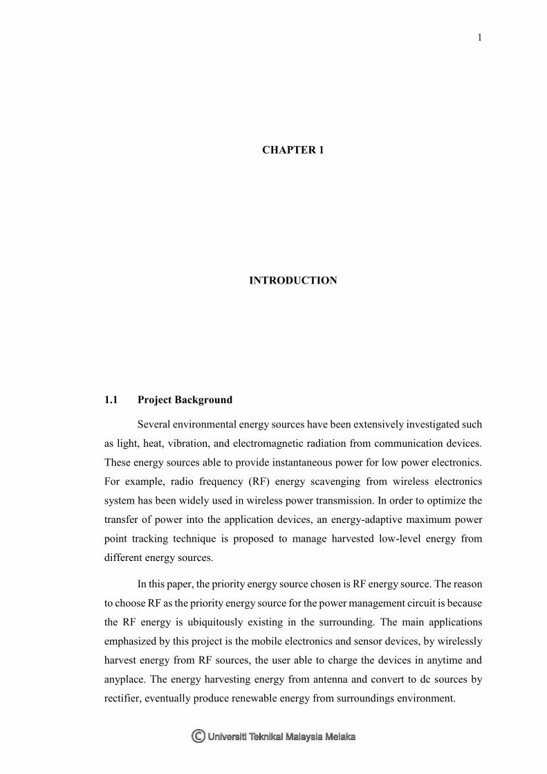
operation [1]. The diagram below shows the typical energy harvesting sensor
application. This paper focuses on the power management block and its interface to
the rectenna and energy storage device [2]. In order to optimize the energy harvested,
the power management system have to generate maximum output power.
Figure 1.1: The diagram shows the typical energy harvesting sensor application
An energy harvesting system normally included components such as energy
harvester or energy transducer, electrical power management or conditioning circuit,
energy storage device and electrical load which are applications. The following section
will discuss about the components in an energy harvesting system.
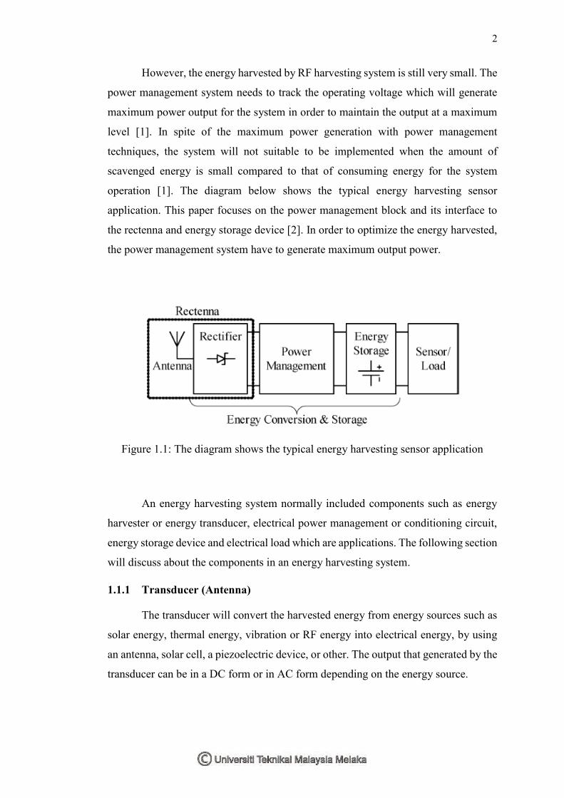
1.1.1 Transducer (Antenna)
The transducer will convert the harvested energy from energy sources such as
solar energy, thermal energy, vibration or RF energy into electrical energy, by using
an antenna, solar cell, a piezoelectric device, or other. The output that generated by the
transducer can be in a DC form or in AC form depending on the energy source.

3
1.1.2 Power conversion (Rectifier)
The power conversion circuit can be a rectifier or DC-DC converter which can
converts the provided energy into a suitable DC voltage. In the block diagram, the
power conversion is a rectifier which convert RF energy to DC source. The efficiency
of the circuit is an important factor which indicates the amount of the useful energy
that can be utilized by the application.
1.1.3 Power management
Power conversion circuit usually have different level for available power
depending on the application, the output voltage of the power conversion circuit can
be regulated to a stable DC voltage using buck or boost converter or it can have limited
by voltage limiter. The power management system controls the conduction path
between the device and energy harvester. A good power management system can to
generate the maximum power output for the energy storage or application devices.
1.1.4 Charge storage
The charge storage is used to keep the charge and store it in a capacitor or a
rechargeable battery or other storage element. When selecting a rechargeable element,
it is important to consider the ability of the battery/capacitor to withstand a high
number of charge/discharge cycles and maintain its performance characteristics.
Super-capacitors, traditional capacitors, and thin film batteries are known for their
ability to retain performance even after a high number of charge/discharge cycles.
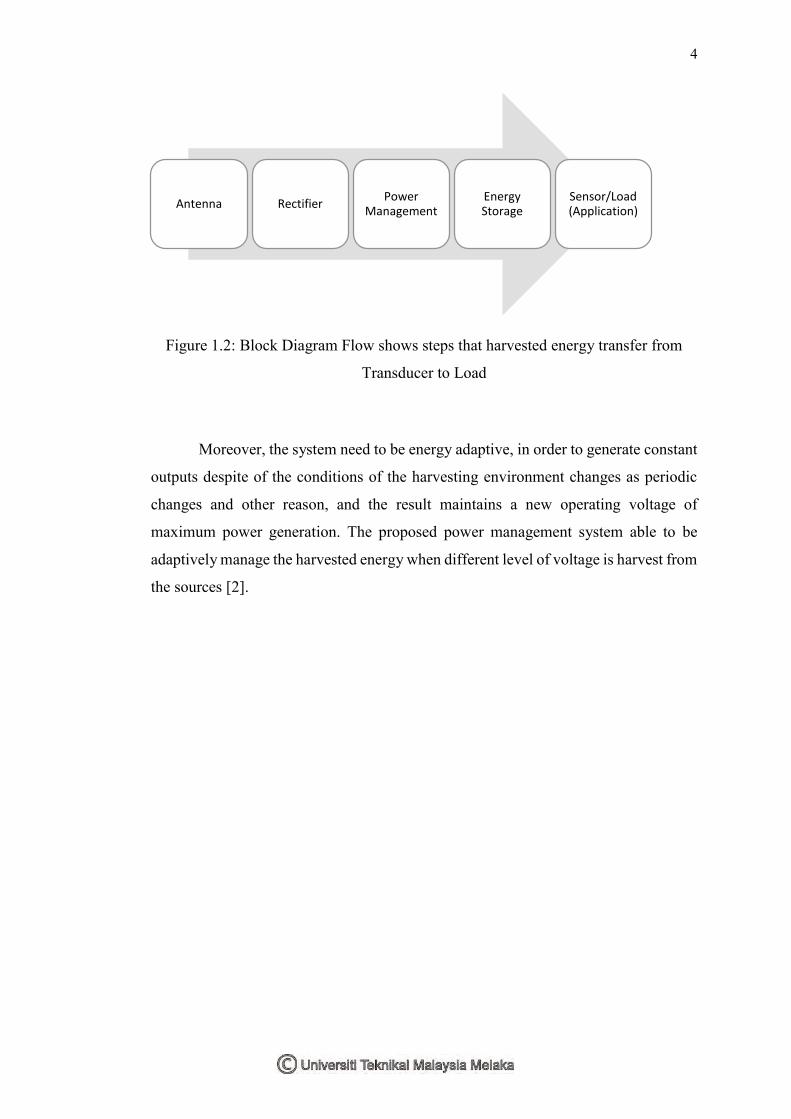
4
Figure 1.2: Block Diagram Flow shows steps that harvested energy transfer from
Transducer to Load
Moreover, the system need to be energy adaptive, in order to generate constant
outputs despite of the conditions of the harvesting environment changes as periodic
changes and other reason, and the result maintains a new operating voltage of
maximum power generation. The proposed power management system able to be
adaptively manage the harvested energy when different level of voltage is harvest from
the sources [2].
Antenna RectifierPower
ManagementEnergy Storage
Sensor/Load (Application)

5
1.2 Problem Statement
Energy harvesting has grown from long-established concepts into devices for
powering ubiquitously deployed sensor networks and mobile electronics. Systems can
scavenge power from human activity or derive limited energy from ambient heat, light,
radio, or vibrations. However, if the ubiquitous and sustainable energy sources are not
use, the energy source will be a waste to the surrounding. As an example, the RF
energy harvesting is developed by the wireless energy transmission technique for
harvesting and recycling the ambient RF energy that is widely broadcasted by many
wireless systems such as mobile communication systems, Wi-Fi base stations, wireless
routers, wireless sensor networks and wireless portable devices. Also, the Internet of
things (IoT) is the upcoming technology that will bring the communication between
devices to the next level. In other words, IoT means there will be Internet everywhere,
and overwhelmed with RF sources. RF energy harvesting is becoming the next
generation trend for mobile electronics devices and wireless sensor system. Imagine
the mobile devices able to harvesting energy to charge the battery while the user is
using the devices or browsing a website by a smartphone. The harvesting will extend
and improve the battery life for the devices and sensors without doubts.
In this project, a power management system will be designed and developed
for performing maximum power point tracking (MPPT) as the fluctuation of the input
power across the target frequency range. The power management system is a miniature
integrated circuit, therefore it is able to implement in the application of mobile
electronics or sensors. The proposed power management circuit will be fabricated.
Before the fabrication process, the power management circuit will be designed in
layout and tested by the standard verification tests.

6
1.3 Objectives
The objectives of the project included:
To investigate techniques and construct adaptive power management system
in miniature size.
To design a power management system to manages low-level energy.
To verify the functionality of the power management system that harvest
energy from ubiquitous energy sources in sensor networks and mobile
electronics.
1.4 Scope of Works
The project is to design an energy-adaptive MPPT power management unit for
harvesting energy from low level power sources. Prior energy sources for the power
management system is energy harvested by RF radiation, yet the power management
unit will have focused on applications that consume power in the order of µW to mW
or even higher in order to implement in more energy scavenging applications. The
proposed power management system will manage input voltage sources by energy-
adaptive MPPT technique, the energy harvested is able to be manage in high efficiency
even when the power level is changed or switched from the harvesting sources.
The schematic circuit design and layout design will be construct by using the
software Synopsis Custom Design. The completed circuit will be tested by verification
test included DRC (Design Rule Check), LVS (Layout Versus Schematic), and PEX
(Practices Extraction). A GDSII file will be created after the verifications tests.

7
CHAPTER 2
LITERATURE REVIEW
2 Overview
In this chapter, the dc biasing analysis and properties of transistor will be
discussed, included the cut-off condition, linear condition and the saturation condition.
Next, the basic methods to analyse the energy and efficiency power management
system will be shown. Moreover, different maximum power point tracking techniques
will be discussed and compared in this chapter.
2.1 DC analysis for MOSFET circuits
In order to design the integrated circuit using Metal-Oxide-Semiconductor-
Field-Effect Transistor (MOSFET), the operation mode need to be assumed and solve
the dc bias utilizing the corresponding current equation. Also, the assumption requires
to be verified with terminal voltages (cutoff, triode and saturation). If the solution is
invalid, change the assumption of operation mode and analyze again.

8
2.1.1 Cut-off
When VGS < VTH, there are no mobility carriers among the channel. There will
be no current conducted in this stage, so ID = 0.
2.1.2 Triode/Linear
In triode or linear stage, the VGS more than VTH, in in this stage the channel
stretches from the source to the drain. The voltage condition for VDS less than VDSat,
where VDSat, VGS − VTH. In other words, when VDS more than VDSat, the channel
stretches from the source to the drain, while when VDS more than VDSat, the channel
stops short of the drain. Also, drifting is the primary mode of current flow. If the
conductive channel achieves, applying VDS will generate an electric field from drain
to source, making electrons flow from source to drain. Therefore, the current able to
flow from drain to source. When the channel that conducts all the way to the drain, the
voltage VDS has to be dropped across the channel. In other words, the electric field will
depend on VDS, means current will depend on VD. Next, VGS will influence the current
since VGS controls the charges in the channel [8]. The ID is representing by the formula
2.1.
ID = 1
2 µn Cox
𝑊
𝐿 [2(VGS − VTH) VDS − VDS
2] (2.1)
The ID depends on both VGS and VDS condition, which the reason that this
region of operation is called triode. The current is also linear with VGS, which is the
region for linear.
2.1.3 Saturation
When VDS more than VDSat, the channel will not go from the source to the drain.
The channel will end before the drain edge or ends at the drain edge for VDS equal to
the VDSat. The effect is pinch-off effect, because the channel is pinched off from the
drain. In this condition, the voltage VDSat is decreased from the source to the edge of
the channel, and the voltage VDS minus VDSat is dropped from the edge of the channel
to the drain. The VDSat is actually not depends on the VDS, in other words the electric

9
field across the channel does not depend on VDS in saturation [8]. The ID in this region
is present by the formula 2.2.
ID = = 1
2 µn Cox
𝑊
𝐿 (VGS − VTH) 2 (2.2)
DC operating regions are very important in circuit design using MOSFET, the
reason is due to the process during designing an analog circuit using complementary
metal-oxide semiconductor (CMOS), and all the transistors should be biased in
Saturation region in order to make sure the circuit is well-performing. This is done in
order to achieve linearity and faithful amplification of the signal in analog circuits. For
biasing of MOSFETs:
Voltage source at the gate and/or a resistor at the source of the MOSFET.
Current source at the source of the MOSFET.
Drain to gate feedback resistor.
2.2 Energy efficiency of power management system
Energy efficiency is a significant factor for low energy harvesting system
design. The conventional energy harvesting systems are low energy efficient in
condition of energy conversion efficiency. Due to the cost and size when designing a
low energy harvesting system, a high efficiency circuit design is needed in order to
reduce the cost and size to achieve small and compact energy generators and energy
storages. The system efficiency of power management system is divided by two type
of efficiencies which included the energy conversion efficiency and energy transfer
efficiency. In this chapter, energy conversion efficiency and the energy transfer
efficiency improvement are discussed.
Energy conversion efficiency represents the total energy harvested by the
energy harvesting system. The energy conversion is very dependent to the features of
the harvesting technology, the capability of the energy harvesting system and the
surrounding environmental conditions. By designing or selecting a high efficient
energy harvester, the energy efficiency can be improved. If the environment energy is

10
Eenergy and the maximum harvested energy of the energy harvester is Eharvested, then the
energy conversion efficiency, ηE,conversion can be expressed as formula 2.3.
ηE,conversion = E harvested
E energy (2.3)
Energy transfer efficiency ηE,transfer determines how much the harvested energy
can available for using. This can be calculated as formula 2.4.
ηE,transfer = E regulated
E harvested (2.4)
where the Eregulated is the regulated energy of the system by a power conversion circuit.
The factors for this condition are the energy able to generated from the energy
harvester and the extracted energy level that able to be transferred to the system. From
[9], the system with a MPPT circuit able to improve a system efficiency by maintaining
the power management system operating at the maximum power point. Therefore, a
MPPT able to improve the energy being generated from the energy harvesting system.
So, the energy Etransducer able to be transferred to the power conversion circuit from the
energy harvesting system, which influence the MPPT efficiency of the MPPT circuit
ηMPPT. Then can be expressed as formula 2.5.
Etransducer = Eharvested • ηMPPT (2.5)
Then Etransducer will be transferred to the power conversion circuit and the
energy will be partly regulated and transferred Eregulated to the following circuit block.
Eregulated is shown in the formula 2.6.

11
Eregulated = Etransducer • ηconversion (2.6)
where ηconversion representing the regulating efficiency of the power conversion circuit.
From formula 2.5 and 2.6 into formula 2.4, ηE,transfer can be rewritten as:
ηE,transfer = E harvested • η MPPT • η conversion
E harvested (2.7)
2.3 Power Management System
In this section, power managements system for energy harvesting devices will
be further discussed. Different power management circuits and Maximum Power Point
Tracking Techniques will be compared in order to select the better power management
techniques for low power applications.
2.3.1 Energy Management System
Energy is generated from the harvesting device and transfer to the energy
storage need a DC-DC conversion, the converter could be a regulator circuit or a power
management circuit. This block should be able to provide the maximum power
generation, the condition can be achieved by controlling the operating voltage and
decreasing the transfer loss with high efficiency [1]. Power management system
including energy storage is the block between energy harvesting circuit and the load.
The main design consideration for power management circuit is to keep the circuit in
a low power consumption condition. Most of energy harvesting methods able to
generate instantaneous power with microwatts, as a result the power management
circuit should be able to designed in a lower power consumption level. Thus, the
ultralow power consumption requirement depends on a period when the device collects
and stores energy from energy harvesting circuit [7].
Usually, the energy harvesting circuit consists of voltage multiplier, rectifier
circuit and storage capacitor. Voltage multiplier able to turn low amplitude AC voltage

12
from energy harvester to higher DC voltage level. The energy harvesting circuit with
voltage multiplier able to be changed with Thevenin voltage and resistance. Thevenin
voltage can be set in the range of 10 V without losses consideration. Next, the Thevenin
resistance should be correspond to the instantaneous power available from different
energy harvesting techniques.
2.3.2 Maximum Power Point
The maximum power from an energy harvesting system able to achieved by
implementing different MPPT techniques. The MPPT keeps the operating voltage of
the harvesting system on a maximum level. Therefore, the harvesting can generate the
energy with maximum power.
2.3.3 Energy-Adaptive MPPT
For the energy-adaptive MPPT technique, the energy harvested is able to be
managed in high efficiency even when the power level is changed or switched from
the harvesting sources. Energy harvested from the surrounding environment could
replace or improve the lifetime of batteries in a wireless sensor network, and RF wave
is a promising source of energy. For example, signal processing may consume 20μ
watts while RF power amplification and transmission consumed approximately 1m
watt. The power management system should activate different blocks or circuit stages
as the input power level changes. To achieve energy-adaptive MPPT control,
information on the absolute or relative amount of available power is needed [4].
The challenge is obtaining and utilizing this information without using power-
demanding computational methods, for example quantizing voltages and currents.
Another difficulty of RF harvesting is to harvest energy efficiently from RF sources
with low power harvested. The energy harvested by RF sources is very dependent on
the signal strength of surrounding environment condition. Next, able to produce high
power conversion efficiency over different range of source voltage without using
switching converters is the challenge during the design of an adaptive energy
management system. For example, available power is measured by a simple hill
climbing method that is actually trial-and-error method. By this method, the power
management circuit able to operate in different modes according to the voltage level
condition [4].
13
Ottman et al. proposed two maximum power point tracking schemes by using
dc-dc converters. Expensive circuit components such as digital signal processor (DSP)
and computation-intensive control algorithms were employed to adaptively adjust the
duty cycle of the dc-dc converters to match the load with the MPP. The design
considerations are not for low voltage and micro-power applications. It is important to
develop a new maximum power point (MPP) tracking method that can provide ultra-
low power overhead and low-cost implementation. Lefeuvre et al. proposed a tracking
scheme that regulates the averaged input resistance of a dc-dc converter to the load
matching resistance of the energy harvesting device [5].
Moreover, D. Maurath compared an adaptive charge pump for dynamic
maximum power point tracking with a novel active full-wave rectifier design. The two
interfaces show different potential operation ranges for harvesting with an actual
electromagnetic transducer. Due to the force-feedback effect of the electromagnetic
transducer the rectifier interface achieves better results over an increased buffer
voltage range of the power management system. However, the charge pump interface
has better performance at high buffer voltages, and can keeps maximum energy on a
buffer capacitor in lower input level. The combination of both interfaces can provide
an autonomous system, which the better interface will be activated at a time dependent
to the actual relative buffer voltage level. The active full wave rectifier uses a common-
gate pseudo-comparator with an output pole. Even in a high resistive sources condition,
the system able to operate stably. The figures below show the active full-wave rectifier
(AFW) configuration uses and active diode schematic design with common-gate
comparator stage, associated biasing, and switch transistor between the diode
terminals anode and cathode [6].

14
Figure 2.1: The active full-wave rectifier configuration uses an active diode [6]
Figure 2.2: Schematic of the active diode [6]
In the bias control stage, the standard circuit topologies are to use a differential
amplifier with current mirror load. Two common-source connected transistors is the
differential pair and an active load formed by the current mirror generates the single-
ended output. The circuit able to provide a very high gain by the bias control stage. A
tail current source is generally used to bias the transistors and this current source can
also control the overall gain of the stage. However, in the design, the transistor is
biasing using a bias voltage applied at the gate of the transistor [6].

15
Figure 2.3: Differential-To-Single ended converter
Figure 2.4 shows the other design proposed by D. Maurath, which is the
adaptive charge pump interface comprises the input-load adapting charge pump.
Figure 2.4: Adaptive charge pump interface comprises the input-load adapting charge
pump [6]
Moreover, the advantage of the power management system is the high
efficiency which approximately 0.9, under a wide range of voltage between 0.5 V and
3.3 V. By using only standard CMOS devices a wide range able to achieved. The
adaptive charge pump gives a dynamic maximum power point tracking. Moreover, the
charge pump also able to operate with AC input voltages, therefore the harvesting
occurs independently from the buffer voltage. Yet, the intrinsic charge pump losses
limit on the performance with efficiency less than 0.48 [6].

16
Figure 2.5: Comparison of harvesting with the AFW and the ACP [6]
Moreover, the off-chip input capacitance provides a better harvesting results
for the interfaces. Also, the auxiliary transducer increases the construction size, yet
making the circuits simple, completely autonomous, and also low duty-cycle systems
due to better handling of high buffer voltages. Both interfaces are fully-integrated in a
0.35µ m CMOS process [6].
In [10], D. Vinko and G. Horvat proposed a power management circuit suitable
for energy harvesting system which operating around 5V voltage level. The energy
harvesting technique operate at low instantaneous power which is not suitable to
provide power continuously to the wireless sensor node. In [7], the operating power
management system, the maximum current that power management circuit produce is
around 100nA. This system suitable for usage with almost all energy harvesting system,
and the system input power operates with 1μW.
17
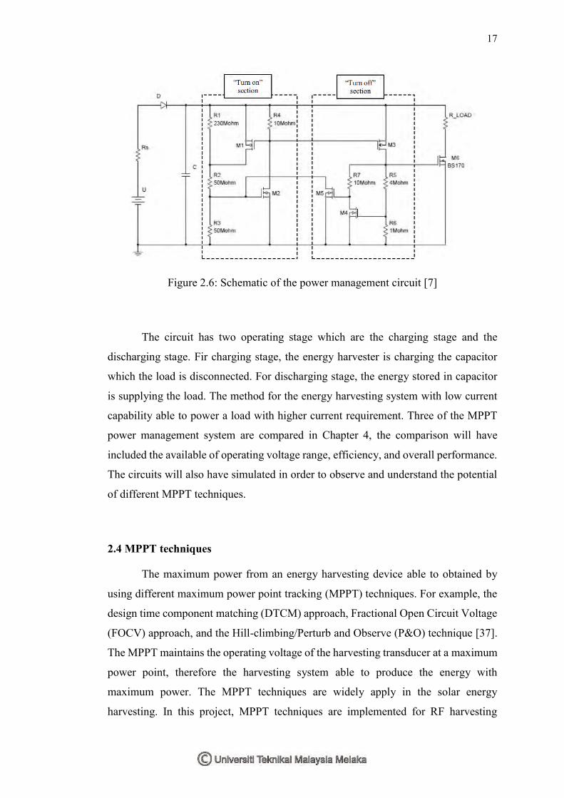
Figure 2.6: Schematic of the power management circuit [7]
The circuit has two operating stage which are the charging stage and the
discharging stage. Fir charging stage, the energy harvester is charging the capacitor
which the load is disconnected. For discharging stage, the energy stored in capacitor
is supplying the load. The method for the energy harvesting system with low current
capability able to power a load with higher current requirement. Three of the MPPT
power management system are compared in Chapter 4, the comparison will have
included the available of operating voltage range, efficiency, and overall performance.
The circuits will also have simulated in order to observe and understand the potential
of different MPPT techniques.
2.4 MPPT techniques
The maximum power from an energy harvesting device able to obtained by
using different maximum power point tracking (MPPT) techniques. For example, the
design time component matching (DTCM) approach, Fractional Open Circuit Voltage
(FOCV) approach, and the Hill-climbing/Perturb and Observe (P&O) technique [37].
The MPPT maintains the operating voltage of the harvesting transducer at a maximum
power point, therefore the harvesting system able to produce the energy with
maximum power. The MPPT techniques are widely apply in the solar energy
harvesting. In this project, MPPT techniques are implemented for RF harvesting
18
condition, and the techniques involved is the P&O techniques and fractional open
circuit voltage techniques. Basically, the P&O technique is a trial and error technique
while the FOCV is the technique that able to adapt in different condition and variation
of the inputs.
2.4.1 Perturbation and Observation (P&O)
In this technique, the voltage and current harvested are measured and the power
value is calculated using multiplier. Given that a small perturbation of voltage or
perturbation of duty cycle of the dc-dc converter, the next stage of the power value is
determined. Compared with the power value of the previous stage, the perturbation is
in the correct direction if next perturbation is larger than current perturbation. In this
way, the maximum power point is recognized and therefore the corresponding voltage
is fixed.
2.4.2 Fractional Open Circuit Voltage (FOCV)
This technique uses the approximately linear relationship between the MPP
voltage (VMPP) and the open circuit voltage (VOC), which varies with the irradiance
and temperature.
VMPP = KVOC (2.8)
K is a constant depending on the characteristics of the PV array and it has to
be determined beforehand by determining the VMPP and VOC for different levels of
irradiation and different temperatures. According to [11] the constant k1 has been
reported to be between 0.78 and 0.92.

19
2.5 Summary of Chapter
This chapter has discussed the dc analysis for standard MOSFET circuit,
included the cut-off region, triode/linear region and the saturation region. Moreover,
different conventional power management circuit and the maximum power tracking
circuit have been discussed and compared. Lastly, the MPPT techniques that applied
in the project, perturbation and observation (P&O) and fractional open circuit voltage
(FOCV) have been discussed in the chapter.

20
CHAPTER 3
METHODOLOGY
3 Overview
The proposed power management system able to manage low power energy
and small in size in order to achieve in the application for mobile electronics and sensor
devices. The software used to design and simulate the schematic and layout is Synopsis,
Full Custom Design and the components library and technology used for the design is
Silterra libraries of 0.13µm and 0.90µm process technology.
The schematic circuit design and layout design will be construct by using the
software Synopsis Custom Design. The completed circuit will be tested by verification
test included DRC (Design Rule Check), LVS (Layout Versus Schematic), and PEX
(Parasitic Extraction). The following flow chart shows the custom design flow for the
design.

21
3.1 Custom Design Flow
The flow chart below shows the custom design flow for the integrated circuit
before the fabrication process.
Figure 3.1: Flow chart for custom design process

22
3.1.1 Project Design Flow
The project flow can be concluded as the process flow in Figure 3.1.1.a. In the
initial stage, different power management system design and circuit topologies will be
compared in term of voltage level, efficiency, size availability and other. The next step
is the design specifications will be further confirmed after considering which
topologies is more suitable for the proposed project design, which is able to manage
low power from harvested RF energy and also suitable for mobile electronics and
devices. After the confirmation of the circuit design, the power management system
will be optimized by different design strategies. Next, standard verification tests will
be carried out in order to further confirm the design potentials.
Figure 3.2: Project flow for designing the power management circuit
Fabrication
Verification
Layout Design
Design Strategies
Design Specifications
Design Comparison

23
3.1.2 Design Comparison
There are three circuits are compared in the stage of Design Comparison:
Adaptive Charge Pump Converter
Common-Gate Stage Active Diode
Voltage Divider Monitoring PMC
Before verification and fabrication process, the circuit design will be optimized to
achieve higher performance on power management. Also, the system has to be energy-
adaptive to different range of voltage sources. The simulation result for common-gate
stage active diode and voltage divider monitoring PMC will show in the following
chapter.
3.1.3 Design Specification
The prior harvesting energy for the adaptive power management circuit is RF
energy. Therefore, the voltage level for the circuit must be low, yet adaptively
managing the harvested energy in different power range. Moreover, the integrated
circuit design has to be small in size in order to achieve the expected specification,
which is able to implement to mobile electronics and sensor device. Therefore, the size
and area of the design has to made as small as possible yet provide optimized
performance. The design challenges included:
Low power consumption
Small in size/area

24
3.1.4 Design Strategies
In this section, the design strategies will be discussed, included the transistors
DC bias operating techniques, parametric optimization, and the optimization for the
size of capacitors and transistors.
3.1.4.1 DC bias operating techniques
In order to ensure that the transistors used in the circuit design work in the
region of interest, usually saturation. The threshold voltage of the transistors is
obtained by printing HSPICE voltages and operating points in Synopsis software. The
width and length of the transistor set in the simulation will change the dc operating
point of the transistor in different conditions. Therefor the dc operating point need to
be obtained to make sure all the circuit is in saturation mode. By using the Synopsis,
the dc operating point of transistor can be obtained by prompt and select a wire from
the schematic for voltage and an instance for operating points. Operating points are
defined by the individual simulator based on the type of device. Once the selection is
made, the results appear in a table.
3.1.4.2 Parametric Optimization
The devices or components used in the design must has configurable
parameters. In order to meet the specifications of the circuit design, the parameters of
the components such as transistors and resistors must be adjusted in order to optimize
the design. For example, transistor gate width and length, or resistor dimensions can
be changed to change their electrical characteristics to match the design requirements.
Figure 3.3: Transistor gate width and length, or resistor

25
3.1.4.3 Optimize the size of capacitors or transistor
In order to minimize the size of the power management circuit design, the size
of the transistors, capacitors and other components need to be optimized. In this project
the techniques use to optimize the performance of the design is using the parametric
analysis tool in the Synopsis Software. The parametric analysis tool is an interactive
analysis that measures performance by simulating a circuit under varying conditions.
Parametric analyses able to define one or more nested sweeps, and you can vary the
value of a design variable for each sweep.
3.2 Schematic Design
Figure 3.4: Flow chart for schematic design process
Layout Design

26
3.3 Layout Design
In the Layout design process, the components presenting in schematic are place
in the new cell view for layout, and the circuit is connecting to each other according
to schematic. During the path connection, designer have to ensure that Layout will not
affect circuit operation. Also, ensure that Layout does not violate fabrication rules. The
aim of Layout design is to lay out a physical view of the schematic, which will operate
the same way.
Figure 3.5: Layout design example
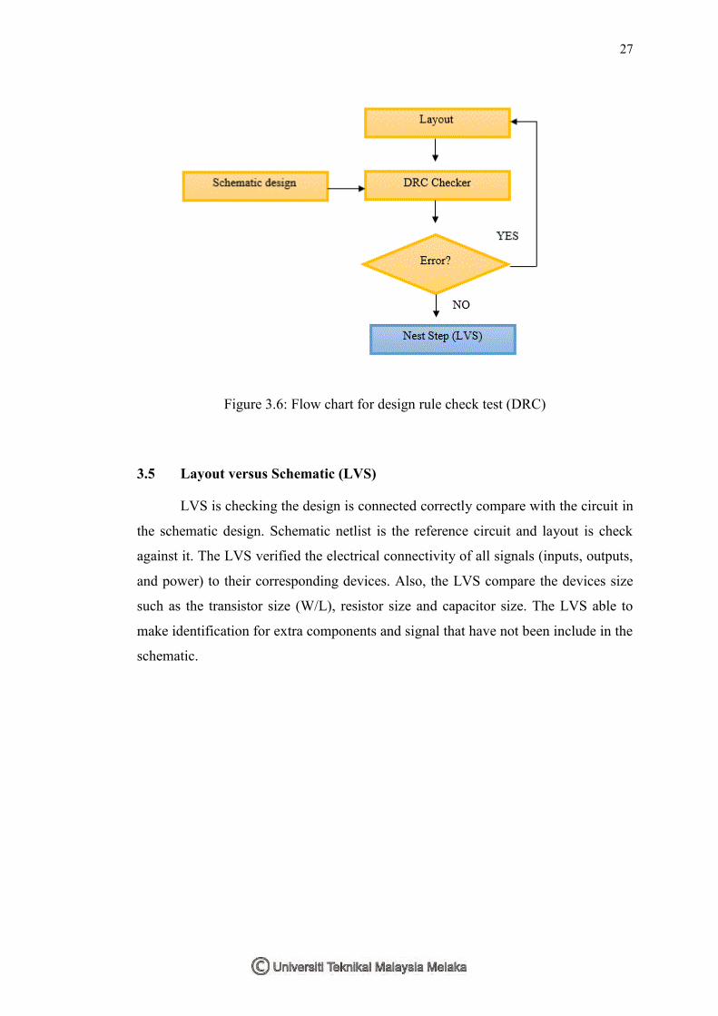
3.4 Design Rule Check (DRC)
The DRC is the checking process design rules and supplementary rules.
Basically, DRC checks all polygons and layers from the layout database to meet all of
the manufacturing process rule. Theoretically, the design rules represent the physical
limits of the manufacturing processes.
27
Figure 3.6: Flow chart for design rule check test (DRC)
3.5 Layout versus Schematic (LVS)
LVS is checking the design is connected correctly compare with the circuit in
the schematic design. Schematic netlist is the reference circuit and layout is check
against it. The LVS verified the electrical connectivity of all signals (inputs, outputs,
and power) to their corresponding devices. Also, the LVS compare the devices size
such as the transistor size (W/L), resistor size and capacitor size. The LVS able to
make identification for extra components and signal that have not been include in the
schematic.
28
Figure 3.7: Flow chart for layout versus schematic test (LVS)
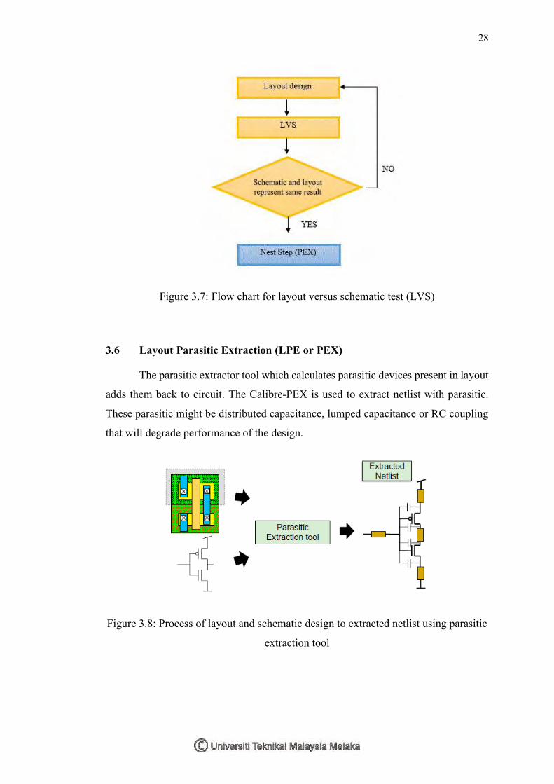
3.6 Layout Parasitic Extraction (LPE or PEX)
The parasitic extractor tool which calculates parasitic devices present in layout
adds them back to circuit. The Calibre-PEX is used to extract netlist with parasitic.
These parasitic might be distributed capacitance, lumped capacitance or RC coupling
that will degrade performance of the design.
Figure 3.8: Process of layout and schematic design to extracted netlist using parasitic
extraction tool
29
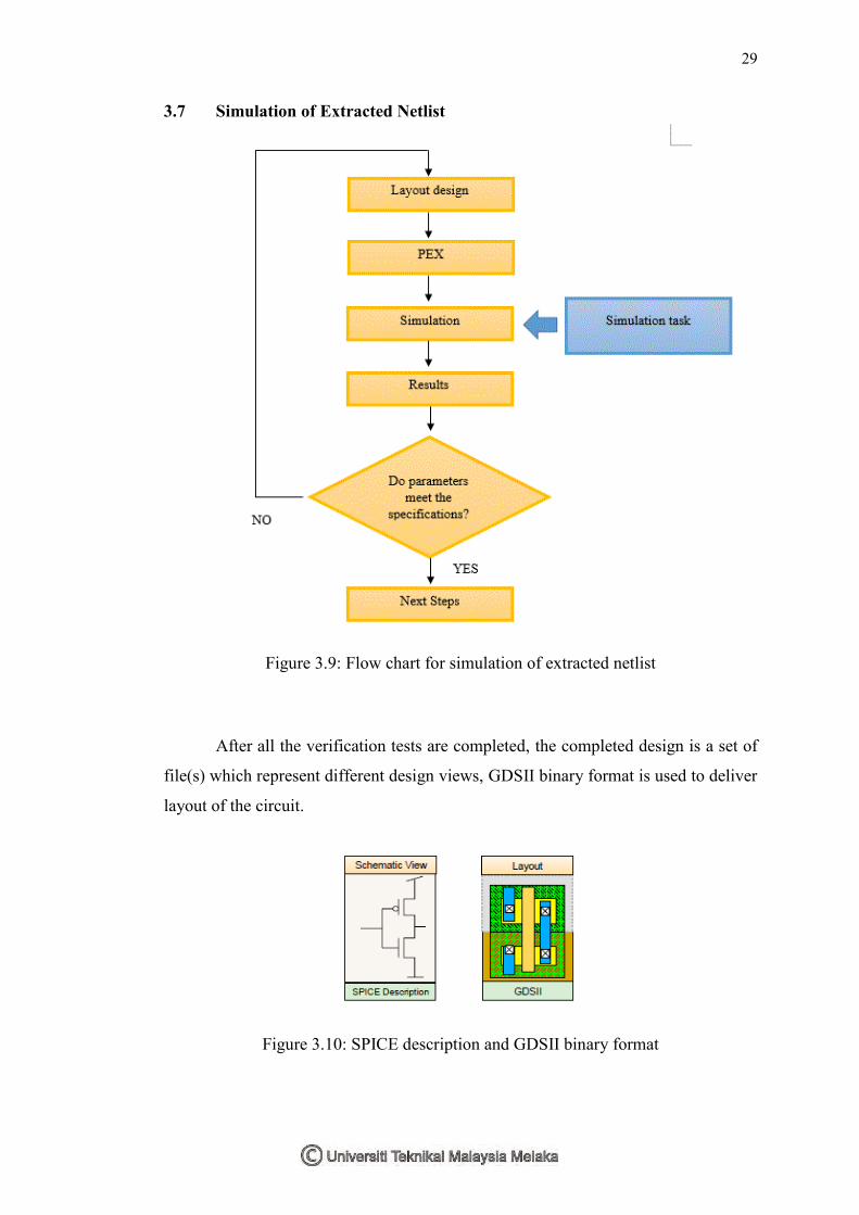
3.7 Simulation of Extracted Netlist
Figure 3.9: Flow chart for simulation of extracted netlist
After all the verification tests are completed, the completed design is a set of
file(s) which represent different design views, GDSII binary format is used to deliver
layout of the circuit.
Figure 3.10: SPICE description and GDSII binary format

30
3.8 Summary of Chapter
This chapter discussed the overall design flow for the project and the
description of each process and design flow. Firstly, the chapter discussed the custom
design flow such as the design review, design specification and design strategies. Next,
the schematic and layout design process were discussed in order to indicates the basic
requirements for CMOS schematic and layout design. Moreover, the verification tests
such as design rules check, layout versus schematic and layout parasitic extraction
process have also been discussed in this chapter.

31
CHAPTER 4
RESULT AND SIMULATION
4 Overview
In this chapter, the simulation results are simulated under Silterra 0.09um and
0.13um process technology. This chapter begins with the comparison and analysis of
different MPPT techniques, and included with the simulation for common-gate stage
active diode. Next, Chapter 4.2 is the main circuit design for this project, which is the
integrated circuit design for analog MPPT decision making circuit. The schematic
design of each blocks for analog circuit design will be shown and discussed with the
simulation result. Then, the parametric optimization of block will be discussed in the
following section with the layout design of selected block. Then the last section is
result and discussion for the digital controlled MPPT circuit. The digitally controlled
MPPT circuit indicates the idea and functionality of MPPT algorithm circuit in form
of digital control.

32
4.1 Comparison and simulation for different MPPT techniques
This subchapter discussed the comparison and analysis of different MPPT
techniques, the simulation for common-gate stage active diode.
4.1.1 Comparison and review of different MPPT techniques
There are three types of power management systems being compared for the
preliminary work, include the adaptive charge pump converter, common-gate stage
active diode, and the voltage divider monitoring power management circuit (PMC).
The common common-gate stage active diode and the voltage divider monitoring
PMC were simulated by using the software Synopsis full custom design, the
parameters of the transistors are set as the research [6] and [7] mentioned, in order to
observe the performance of the power management circuits. The common common-
gate stage active diode design consists of N-MOS and P-MOS, which the width of the
P-MOS is 80µm and length is 3µm while the N-MOS is 60µm in width and 3µm in
length. For voltage divider monitoring PMC, also included the N-MOS and P-MOS in
the design, the width and length of the N-MOS and P-MOS would be simulated in
variable parameter in order to obtain optimized performance.
The common-gate stage active diode and the voltage divider monitoring power
management circuit has been simulated in the software Synopsis Full Custom Design,
the parameters of the circuit are set according to the proposed design in literature
review in order to observe the power management circuit performance. The following
section shows the simulation results for the common-gate stage active diode, and the
voltage divider monitoring PMC, comparing the input source will output voltage that
the circuits can perform. The efficiency of the simulation circuit will be calculated and
compared with the literature review.

33
Table 4.1: Comparison of Different MPPT Power Management Circuit
Adaptive Charge
Pump Converter
Common-Gate
Stage Active
Diode
Voltage Divider
Monitoring PMC
Input Voltage
Range
0.5V – 2.5V 0.48V up to 3.3V Up to 5V
Efficiency close to 50% 90% -
Pros -Most beneficial
for high buffer
voltage
-Storing maximum
energy even with -
-Low input
amplitudes
-Able to handle
AC input voltages
-Better result for
increased buffer
voltage range
-Low voltage drop
(below 30mV) at
all voltage level
-Low complexity
ultra-low power
consumption
-Operating voltage
level is 5V.
-Maximum current
draws under
100nA
-Suitable for most
energy harvesting
methods
Cons -Lower efficiency - Not adaptive to
different power
inputs
-Low charging
current
-Charging time
higher
4.1.2 Schematic Circuit for Common-Gate Stage Active Diode
The common-gate stage active diode is simulated by using the software
Synopsis custom design, the technology used is 0.09um process technology. Figure
4.1 shows the complete schematic circuit for common-gate stage active diode with
labelled stages. Then, the following figures will indicate the schematic circuit of each
stages.
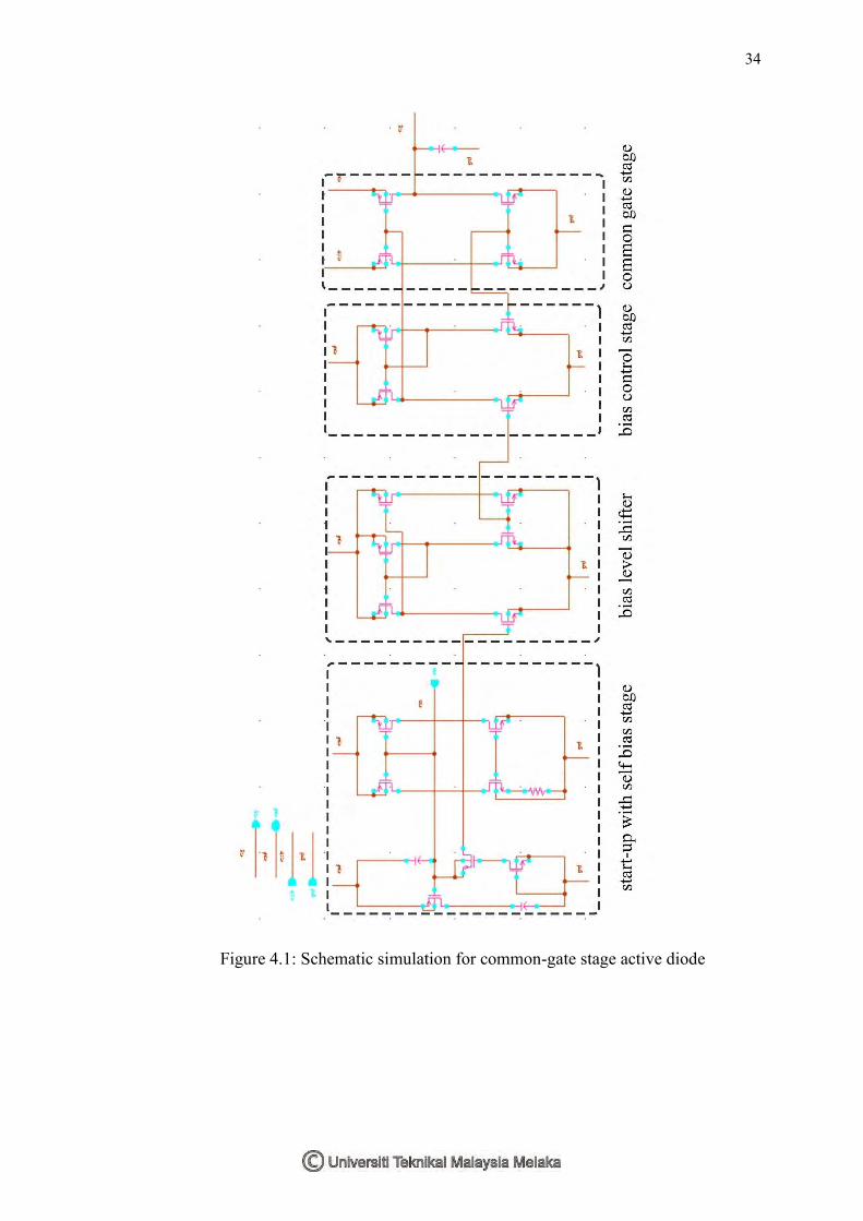
34
Figure 4.1: Schematic simulation for common-gate stage active diode
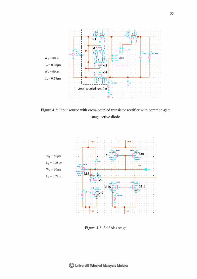
35
Figure 4.2: Input source with cross-coupled transistor rectifier with common-gate
stage active diode
Figure 4.3: Self bias stage
Wp = 80µm
Lp = 0.28µm
Wn = 60µm
Ln = 0.28µm
Wp = 80µm
Lp = 0.28µm
Wn = 60µm
Ln = 0.28µm

36
Figure 4.4: Bias level shifter
Figure 4.5: Bias control stage & CG stage
Wp = 80µm
Lp = 0.28µm
Wn = 60µm
Ln = 0.28µm
Wp = 80µm
Lp = 0.28µm
Wn = 60µm
Ln = 0.28µm

37
Figure 4.6: Switch circuit
4.1.3 Simulation Results for Common-Gate Stage Active Diode
The AC voltage set at the input is 0.6V, the voltage after the cross-coupled
transistor rectifier is 0.581V. The capacitor for buffering is 10µF, and the buffering
voltage for the simulation is 0.554V.
Figure 4.7: Simulation for common-gate stage active diode at 0.6V
Wp = 99µm
Lp = 0.28µm
0.581V
0.554V
38
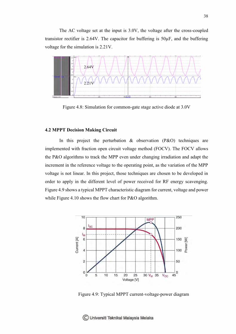
The AC voltage set at the input is 3.0V, the voltage after the cross-coupled
transistor rectifier is 2.64V. The capacitor for buffering is 50µF, and the buffering
voltage for the simulation is 2.21V.
Figure 4.8: Simulation for common-gate stage active diode at 3.0V
4.2 MPPT Decision Making Circuit
In this project the perturbation & observation (P&O) techniques are
implemented with fraction open circuit voltage method (FOCV). The FOCV allows
the P&O algorithms to track the MPP even under changing irradiation and adapt the
increment in the reference voltage to the operating point, as the variation of the MPP
voltage is not linear. In this project, those techniques are chosen to be developed in
order to apply in the different level of power received for RF energy scavenging.
Figure 4.9 shows a typical MPPT characteristic diagram for current, voltage and power
while Figure 4.10 shows the flow chart for P&O algorithm.
Figure 4.9: Typical MPPT current-voltage-power diagram
2.64V
2.21V

39
Figure 4.10: Perturbation and observation algorithm flow chart
4.2.1 MPPT Algorithm (Analog)
The MPPT circuit usually able to control by analog circuit or the digital control.
For analog MPPT circuit, the method uses an analog circuitry and a classical feedback
control to create an energy scavenging system. The main characteristic for analog
MPPT circuit is simplicity, low overhead and low cost. Digital controlled MPPT will
be further discuss in Chapter 4.3. Figure 4.11 shows the complete MPPT decision
making circuit for this project which consists of multiplier, sample and hold circuit,
comparator, D flip flop and the XNOR gate. The circuit is simulated under the
condition of the inputs below 1.5V in order to suit the RF energy scavenging condition.

40
Figure 4.11: Complete MPPT decision making circuit
4.2.2 Multiplier
The multiplier used in the MPPT design is a four quadrants analog multiplier
which consists of a multiplier cell, a mixed signal circuit and signal subtraction circuits.
The design has single ended inputs, the geometry of all transistors are equal, and the
output can be the product of two signal voltages, or the product of a signal current and
a signal voltage [12]. The proposed multiplier in [17] is a low-voltage low-power
CMOS RF four-quadrant multiplier which simulated in standard 0.5μm CMOS [17].
The proposed multiplier is simulated in 0.13μm Silterra process technology. Basically,
multiplier is used to evaluate the power (V*I), eliminating the need of analog to digital
conversion hardware. From Figure 4.12, the transistor M1 until M8 are pmos from
Silterra 0.13µm process technology library, while M9 until M16 are nmos from the
Silterra library. Wp is the width of the pmos while Lp is the length of the pmos, Wn is
the width of the nmos while Ln is the length of the nmos. The parameters for both nmos
and pmos have not being optimized by parametric optimization in this stage.

41
Figure 4.12: Schematic circuit for multiplier
A subtractor circuit is added to the in order to subtract the two outputs value of
the multiplier, and eventually represents as the output of multiplier before connected
to the comparator. The subtractor circuit is a differential amplifier which consists of
resistors R1 and R2 and Op-amp circuit. M1 to M3 are pmos transistor which using
the same width and length as multiplier, while M4 to M8 are nmos transistor. Figure
4.13 shows the schematic circuit for the subtractor. The output voltage represents as
the Formula 4.1.
Vout = 𝑅2
𝑅1 (V2 – V1) (4.1)
Wp = 3µm
Lp = 0.13µm
Wn = 4µm
Ln = 0.13µm
42
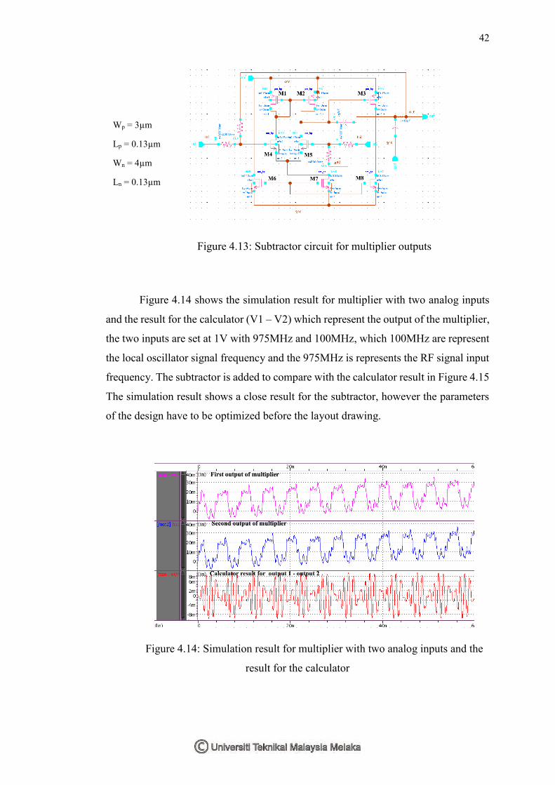
Figure 4.13: Subtractor circuit for multiplier outputs
Figure 4.14 shows the simulation result for multiplier with two analog inputs
and the result for the calculator (V1 – V2) which represent the output of the multiplier,
the two inputs are set at 1V with 975MHz and 100MHz, which 100MHz are represent
the local oscillator signal frequency and the 975MHz is represents the RF signal input
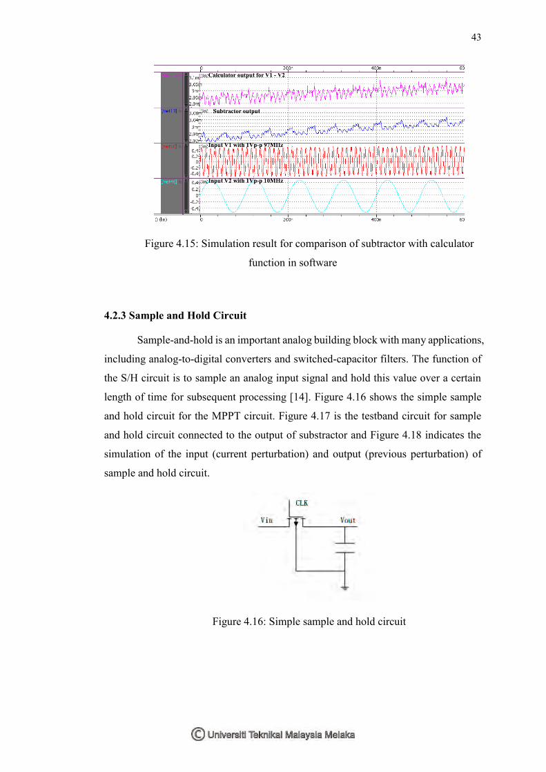
frequency. The subtractor is added to compare with the calculator result in Figure 4.15
The simulation result shows a close result for the subtractor, however the parameters
of the design have to be optimized before the layout drawing.
Figure 4.14: Simulation result for multiplier with two analog inputs and the
result for the calculator
Wp = 3µm
Lp = 0.13µm
Wn = 4µm
Ln = 0.13µm
43
Figure 4.15: Simulation result for comparison of subtractor with calculator
function in software
4.2.3 Sample and Hold Circuit
Sample-and-hold is an important analog building block with many applications,
including analog-to-digital converters and switched-capacitor filters. The function of
the S/H circuit is to sample an analog input signal and hold this value over a certain
length of time for subsequent processing [14]. Figure 4.16 shows the simple sample
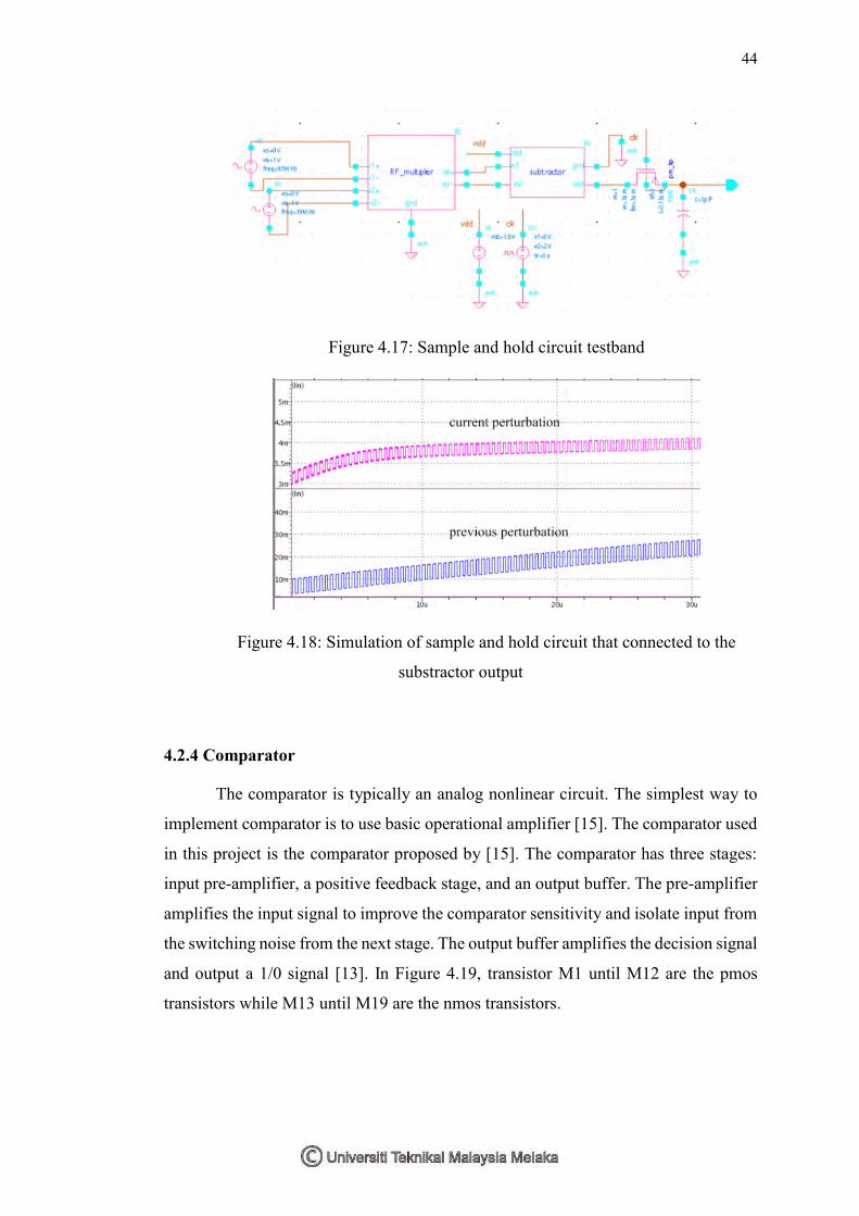
and hold circuit for the MPPT circuit. Figure 4.17 is the testband circuit for sample
and hold circuit connected to the output of substractor and Figure 4.18 indicates the
simulation of the input (current perturbation) and output (previous perturbation) of
sample and hold circuit.
Figure 4.16: Simple sample and hold circuit
44
Figure 4.17: Sample and hold circuit testband
Figure 4.18: Simulation of sample and hold circuit that connected to the
substractor output
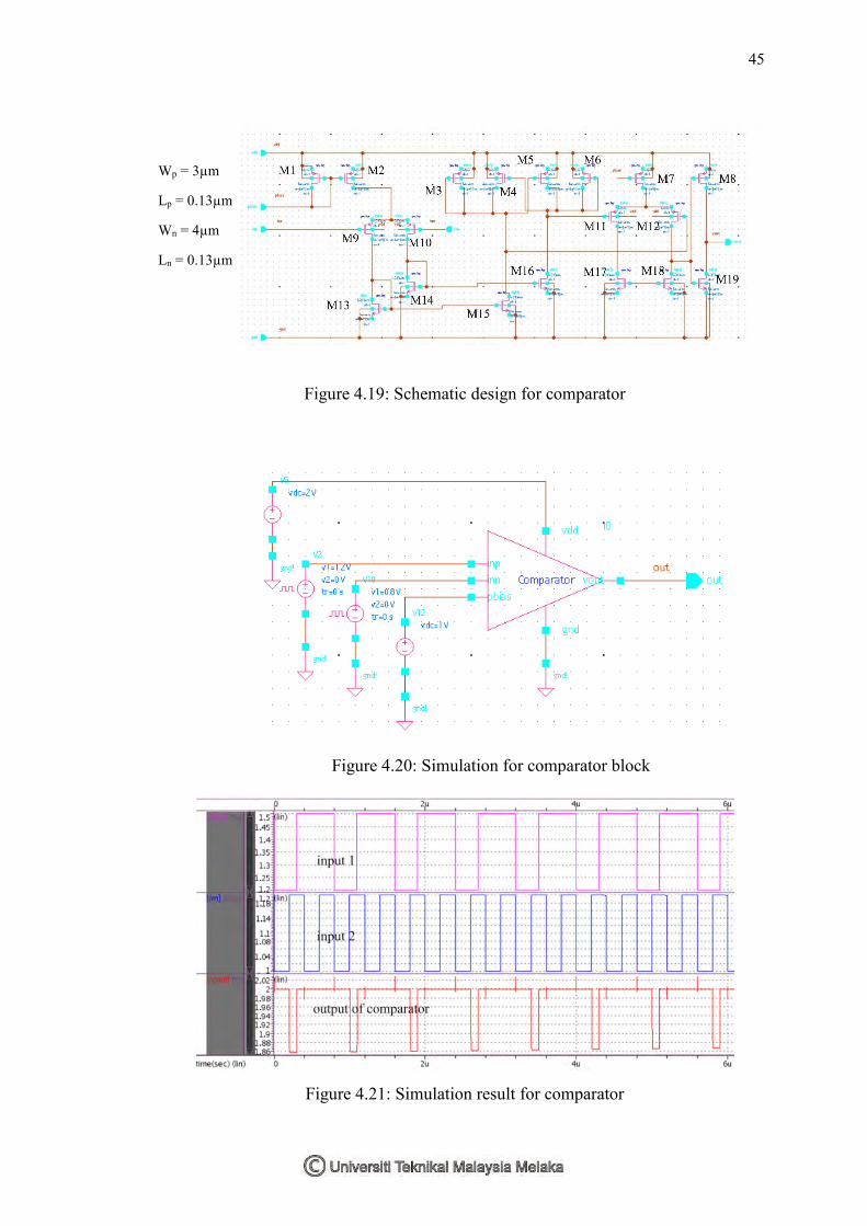
4.2.4 Comparator
The comparator is typically an analog nonlinear circuit. The simplest way to
implement comparator is to use basic operational amplifier [15]. The comparator used
in this project is the comparator proposed by [15]. The comparator has three stages:
input pre-amplifier, a positive feedback stage, and an output buffer. The pre-amplifier
amplifies the input signal to improve the comparator sensitivity and isolate input from
the switching noise from the next stage. The output buffer amplifies the decision signal
and output a 1/0 signal [13]. In Figure 4.19, transistor M1 until M12 are the pmos
transistors while M13 until M19 are the nmos transistors.
45
Figure 4.19: Schematic design for comparator
Figure 4.20: Simulation for comparator block
Figure 4.21: Simulation result for comparator
Wp = 3µm
Lp = 0.13µm
Wn = 4µm
Ln = 0.13µm
46
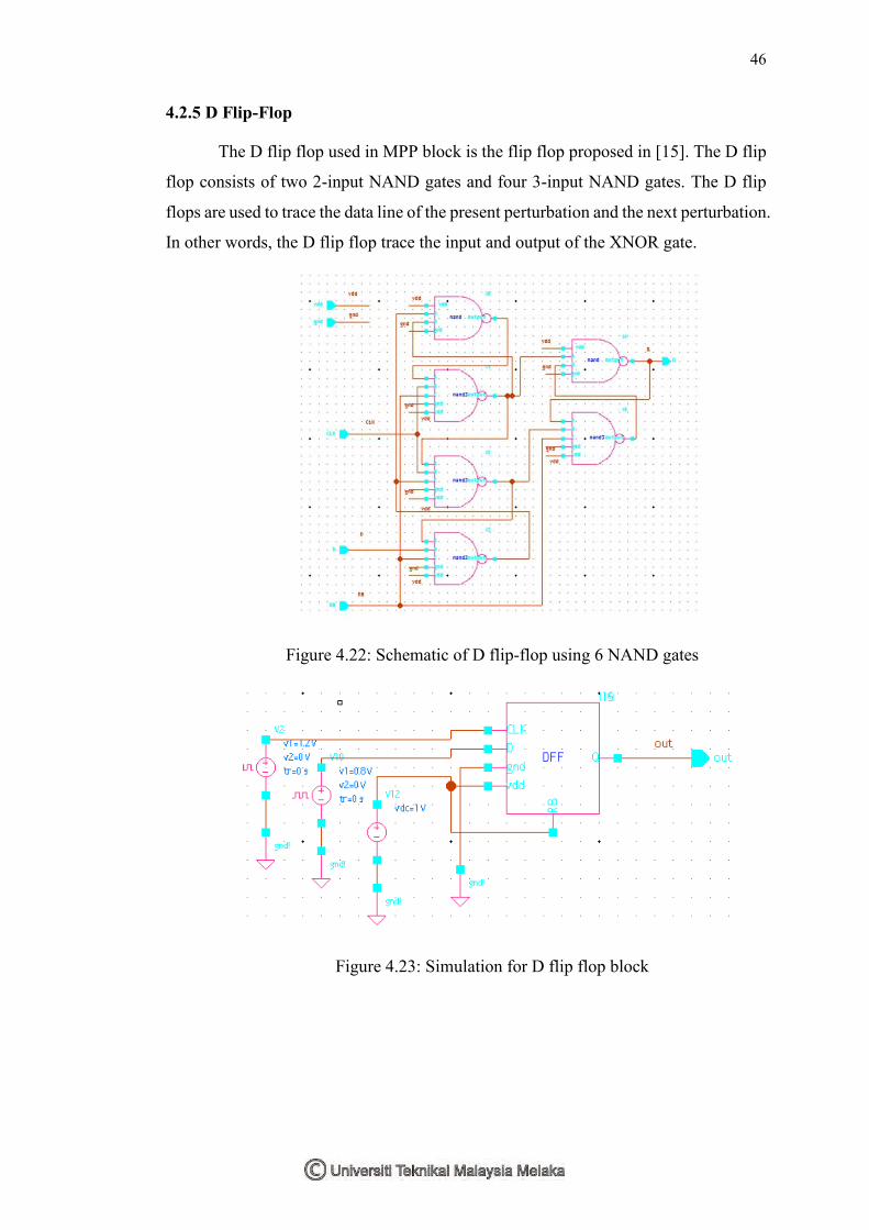
4.2.5 D Flip-Flop
The D flip flop used in MPP block is the flip flop proposed in [15]. The D flip
flop consists of two 2-input NAND gates and four 3-input NAND gates. The D flip
flops are used to trace the data line of the present perturbation and the next perturbation.
In other words, the D flip flop trace the input and output of the XNOR gate.
Figure 4.22: Schematic of D flip-flop using 6 NAND gates
Figure 4.23: Simulation for D flip flop block
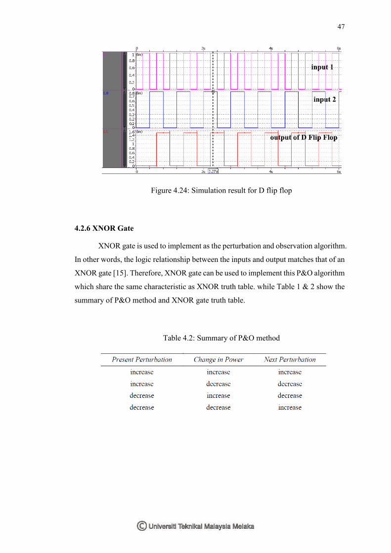
47
Figure 4.24: Simulation result for D flip flop
4.2.6 XNOR Gate
XNOR gate is used to implement as the perturbation and observation algorithm.
In other words, the logic relationship between the inputs and output matches that of an
XNOR gate [15]. Therefore, XNOR gate can be used to implement this P&O algorithm
which share the same characteristic as XNOR truth table. while Table 1 & 2 show the
summary of P&O method and XNOR gate truth table.
Table 4.2: Summary of P&O method

48
Table 4.3: Truth table of P&O method
The output from two D flip-flops which trace the input and output data line will
send to the XNOR Gate in order to achieve MPPT algorithm. Figure 4.25 shows the
schematic design for XNOR gate in Synopsis schematic cell view. Next, Figure 4.26
is the simulation testband design for XNOR gate, while Figure 4.27 shows the
simulation result for XNOR gate when input 2 is keep in HIGH condition and input 1
is vary as 1/0.
Figure 4.25: Schematic of XNOR gate

49
Figure 4.26: XNOR gate block testband
Figure 4.27: Simulation result for XNOR gate
4.2.7 Simulation Result and Discussion
The simulation results show the operation of the new MPPT controller of the
P&O method. Figure 4.28 shows the of simulation result for sample timing diagram.
The first row of Figure 4.28 is the current perturbation (m-1), second row is the next
perturbation (m), the third and fourth row are the clock (clk) and the comparator output
(cmd). Next, the Q1 and Q2 represent the output of first flip flop and second flip flop.
The timing diagram shows the operation of the proposed MPPT controller of the P&O
method. As the new perturbation cycle begins at the rising edge of clock. The
perturbation direction for next cycle will be determined based on the comparison

50
results of m and m-1, where m represents the sampled result of harvested power in the
present cycle and m-1 is the stored harvested power value in the last cycle. Thus, the
capacitor in the storage cell will be charged (discharged). Basically, the comparator
output, cmd is updated at the rising edge of clk (pulse from oscillator-clock input) and
the outputs of the two flip-flops are refreshed at the rising edge of clock. If the m is
greater (smaller) than m-1, the capacitor will be charged (discharged). And once its
voltage is higher (lower) than m, the cmd (comparator output) will toggle and
discharge/charge ends. The variation of both input for comparator will vary the cmd,
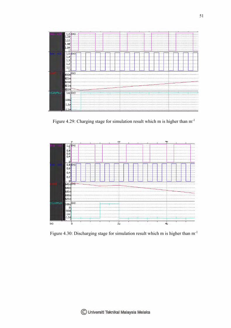
which controlling the duty cycle of the whole circuit. Next, Figure 4.29 shows the
simulation result for the Vref (XNOR gate output with energy storage) in charging
state while Figure 4.30 shows the simulation result for discharging state.
Figure 4.28: Sample timing diagram for MPPT decision making circuit
The cmd is controlling the duty cycle of the analog MPPT circuit which the
duty cycle will vary depend on the condition of both inputs of the comparator (m and
m-1). For example, Figure 4.28 indicates the charging stage for the circuit without
energy storage, which first perturbation input m is higher than the second perturbation
input m-1. If the condition which inverse, the m-1 is higher than m, the duty cycle will
shift the direction of the signal. Also, the width of the duty cycle depends on the
conditions for both inputs of comparator.
51
Figure 4.29: Charging stage for simulation result which m is higher than m-1
Figure 4.30: Discharging stage for simulation result which m is higher than m-1
52
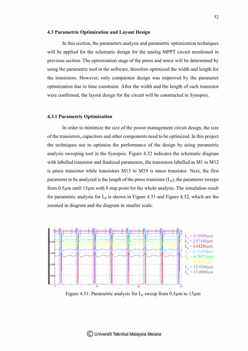
4.3 Parametric Optimization and Layout Design
In this section, the parameters analysis and parametric optimization techniques
will be applied for the schematic design for the analog MPPT circuit mentioned in
previous section. The optimization stage of the pmos and nmos will be determined by
using the parametric tool in the software, therefore optimized the width and length for
the transistors. However, only comparator design was improved by the parameter
optimization due to time constraint. After the width and the length of each transistor
were confirmed, the layout design for the circuit will be constructed in Synopsis.
4.3.1 Parametric Optimization
In order to minimize the size of the power management circuit design, the size
of the transistors, capacitors and other components need to be optimized. In this project
the techniques use to optimize the performance of the design by using parametric
analysis sweeping tool in the Synopsis. Figure 4.32 indicates the schematic diagram
with labelled transistor and finalized parameters, the transistors labelled as M1 to M12
is pmos transistor while transistors M13 to M19 is nmos transistor. Next, the first
parameter to be analyzed is the length of the pmos transistor (Lp), the parameter sweeps
from 0.5µm until 15µm with 8 step point for the whole analysis. The simulation result
for parametric analysis for Lp is shown in Figure 4.31 and Figure 4.32, which are the
zoomed in diagram and the diagram in smaller scale.
Figure 4.31: Parametric analysis for Lp sweep from 0.5µm to 15µm

53
Figure 4.32: Parametric analysis for Lp (small scale)
The variation for the output of comparator by sweeping the parameter Lp is
actually is low. Therefore, the parameter for Lp is set as low as possible in order to
reduce the total sizing for the comparator. Next, the width W is analyzed, the width
for both pmos (Wp) and nmos (Wn) shared the same value for the comparator, as a
result the widths will be analyzed by using the same variable value. The width of the
transistor is sweep from 0.5µm to 20µm with 8 step points in order to observe the
variation for the increasing width. Figure 4.33 shows the parametric analysis for the
width parameter. It is found that the smaller width will actually maintain more constant
output for the comparator. The first line of the graph is actually representing the 0.5µm
condition, then same goes to following defined width values.
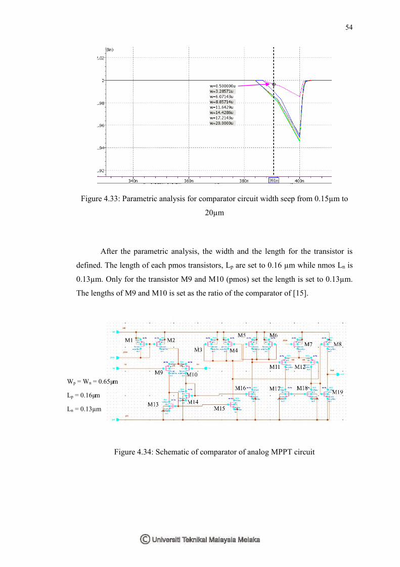
54
Figure 4.33: Parametric analysis for comparator circuit width seep from 0.15µm to
20µm
After the parametric analysis, the width and the length for the transistor is
defined. The length of each pmos transistors, Lp are set to 0.16 µm while nmos Ln is
0.13µm. Only for the transistor M9 and M10 (pmos) set the length is set to 0.13µm.
The lengths of M9 and M10 is set as the ratio of the comparator of [15].
Figure 4.34: Schematic of comparator of analog MPPT circuit
Wp = Wn = 0.65µm
Lp = 0.16µm
Ln = 0.13µm

55
4.3.2 Layout Design
In the Layout design process, the components presenting in schematic are place
in the new cell view for layout, and the circuit is connecting to each other according
to schematic. After the parameters of the comparator was confirmed, the layout of the
comparator is designed according to the design rules and techniques. The basic layout
techniques used in the layout design included matching single transistor, multiple
fingers, interdigitated devices, common centroid, dummy, and folded cascade
amplifier.
4.3.2.1 Matching Single Transistor
A CMOS transistor basically crossed with two rectangles, polysilicon and
active area. Each transistor of the design should be arranged in same orientation for
the layout design as the current for the circuit flowing in the same direction.
4.3.2.2 Multiple Fingers
Multiple fingers layout design is more preferable to reduce parasitic
capacitance and the resistance. By divide the transistor into multiple fingers also able
to split the layout area in order to fulfill design requirement.
4.3.2.3 Interdigitated devices
The interdigitated pattern used for the layout design for the comparator is a
four finger design, the pattern is shown as the configuration in Figure 4.36.

56
Figure 4.35: Typical circuit use for interdigitated transistor
Figure 4.36: Configuration of interdigitated pattern
4.3.2.4 Dummy
The dummy pattern may be formed to reduce the production tolerance. It is
important to maintain the same environment on the two side of the axis symmetry, the
dummy happened when one metal line passing over only one of the transistor indeed
degrade the symmetry and increasing the mismatch. The path need to be connected as
both ends of the same drains or sources connection.
Figure 4.37: Dummy transistor
57
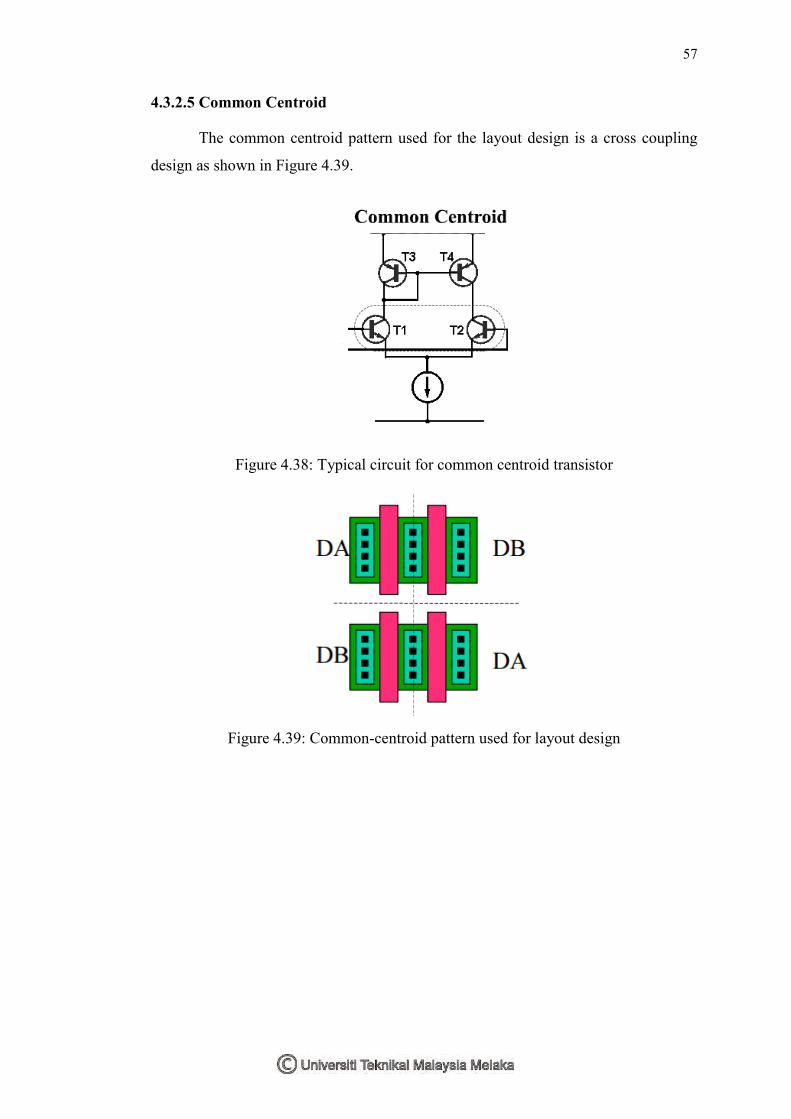
4.3.2.5 Common Centroid
The common centroid pattern used for the layout design is a cross coupling
design as shown in Figure 4.39.
Figure 4.38: Typical circuit for common centroid transistor
Figure 4.39: Common-centroid pattern used for layout design
58
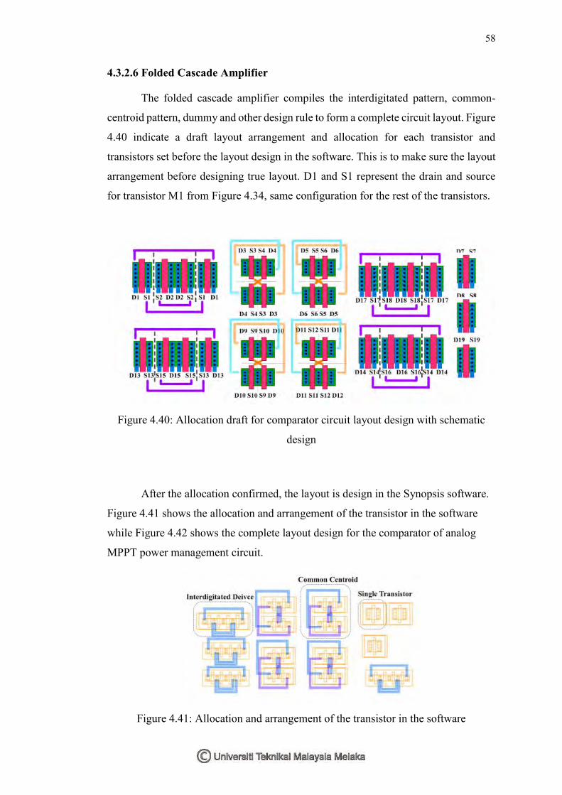
4.3.2.6 Folded Cascade Amplifier
The folded cascade amplifier compiles the interdigitated pattern, common-
centroid pattern, dummy and other design rule to form a complete circuit layout. Figure
4.40 indicate a draft layout arrangement and allocation for each transistor and
transistors set before the layout design in the software. This is to make sure the layout
arrangement before designing true layout. D1 and S1 represent the drain and source
for transistor M1 from Figure 4.34, same configuration for the rest of the transistors.
Figure 4.40: Allocation draft for comparator circuit layout design with schematic
design
After the allocation confirmed, the layout is design in the Synopsis software.
Figure 4.41 shows the allocation and arrangement of the transistor in the software
while Figure 4.42 shows the complete layout design for the comparator of analog
MPPT power management circuit.
Figure 4.41: Allocation and arrangement of the transistor in the software

59
Figure 4.42: Complete layout design for the comparator of analog MPPT power
management circuit
4.4 Digital Controlled MPPT by microcontroller
Digital MPPT circuit uses microcontroller unit (MCU) based with digital and
adaptive algorithm to track MPP of the system. Compared to analog design, power
consumption is the main challenge for using digital in the micro energy scavenging
system. A digital MPPT circuit is constructed for this project in order to indicates the
functionality and concept of the related MPPT techniques. The digital MPPT circuit is
controlled by using Arduino microcontroller. The digital MPPT circuit shared the same
algorithm (P&O) with the analog MPPT design of this project.
4.4.1 MPPT Algorithm (Digital)
The Arduino model used in the prototype is Arduino Mega 2560, and work
together with buck converter circuit, half bridge driver, rectifier (input), energy storage
and the voltage and current measurement circuit. The buck converter consists of three
power MOSFET, IRFZ44N. The half bridge driver is IR2104, and energy storage is a
two 1.2V rechargeable batteries. The voltage measurement is constructed by a basic
voltage divider circuit while the current measurement circuit is constructed by using
current sensor, MAX2473+. Figure 4.43 shows the block diagram of the digital MPPT
circuit while Figure 4.44 shows the schematic design for the digital MPPT circuit
without the voltage and current measurement circuit.

60
Figure 4.43: Block diagram for digital MPPT circuit
Figure 4.44: Schematic circuit diagram for digital MPPT circuit
4.4.2 Operation modes of circuit
There are 5 operation stage for the MPPT algorithm circuit where the charger modes
able to switch or change the operation mode according to the conditions of input power
and batteries power. The five operation modes included:
Buck Mode
Float Mode
Sleep Mode
No battery Mode
Discharging Mode

61
4.4.2.1“Buck” Mode
Buck mode is where the batteries start to charge by the buck circuit. The controller
will send a HIGH signal to the IR2104 where the IC driver will turn on the gate of the
power MOSFET to charge the batteries by the input power. The power MOSFET will
be turned on, thus Enabled plotted ON and indicated on the serial monitor.
4.4.2.2“Float” Mode
Float mode is the condition when the batteries still able to supply enough energy, after
the voltage drops until the low battery level, the batteries will switch the mode “Buck”
mode in order to charge the battery.
4.4.2.3“Sleep” Mode
Sleep mode is where the input voltage is in low voltage condition where there is less
supply to circuit, there will be no charging process in the mode. The circuit will turn
into mode when the input voltage is less than 3V.
4.4.2.4“No battery” Mode
No battery mode is the condition where the batteries is removed or the batteries voltage
level is drops to a low level without charging process. The limit set for the battery
voltage is 1.2V as the battery used is 2.48V.
4.4.2.5“Discharging” Mode
Discharging mode is the stage where the batteries power is used by the load provided.

62
Figure 4.45: Operation mode under different voltage conditions for the MPPT circuit
4.4.2 Prototype using Arduino as microcontroller unit
Figure 4.46 shows the circuit constructed on breadboard, the prototype circuit
contains voltage and current measurement circuit for both input and batteries, half
bridge driver, buck converter, rechargeable batteries and the Arduino Mega 2560
which connected to a personal computer. However, the MPPT circuit in this project,
load is not included in the circuit. Therefore, the batteries have to be discharged
manually.
Figure 4.46: Prototype of digital MPPT circuit

63
4.4.3 Serial Monitor Print and Serial Plotter Print
The prototype for digital MPPT circuit able to measure the input voltage, input
current, batteries voltage and current of voltage, therefore the power for both input and
batteries able to calculate by the system. The variation of the voltages of input and
batteries will switch the modes of the system depend on the voltage conditions. Then,
the analog input of voltage and current will be determined by the microcontroller, the
PWM variation depend on the voltages condition and follow the characteristic of P&O
algorithm. The PWM values is the main element for the MPPT controlling algorithm.
In other words, the PWM is actually works as the duty cycles changes as the analog
MPPT circuit mentioned in previous chapter. The percentage of PWM will be
increased or decreased according to the P&O algorithm, in order to change the
direction of the harvester system. Figure 4.47 shows the result printed on the serial
monitor of Arduino software while Figure 4.48 shows the voltages for both input and
the batteries on the serial plot of Arduino software.
Figure 4.47: Serial monitor printing for the results of digital MPPT circuit

64
Figure: 4.48: Serial plotter printing the input voltage and batteries voltage in real-
time
4.5 Summary of Chapter
In this chapter, a power management system has been designed and developed
for performing maximum power point tracking (MPPT) techniques as the fluctuation
of the input power across the target frequency range. The MPPT techniques involved
in the paper are the perturbation and observation (P&O) and the fractional open circuit
voltage (FOCV). The analog MPPT circuit control the charging and discharging stage
by the duty cycle which depends on the variation of harvested power. The circuit will
be simulated and designed using standard 0.13μm Silterra process technology.
Next, the comparator of the analog MPPT decision making block were selected
to optimize and construct in this paper, the parameters of the comparator circuit has
been optimized and minimized. In order to ensure accuracy result of the circuit, several
layout design rules such as common centroid, interdigitated transistor, folded cascaded
amplifiers are applied in the layout design of the comparator block.
Lastly, a digitally control MPPT circuit which controlled by microcontroller
unit (MCU) is constructed to control the operation stages and generate maximum
power point. The method that implemented in this project is perturbation and
observation (P&O) algorithm which is using same algorithm as the proposed analog
MPPT circuit. The microcontroller unit control the condition of the buck convertor
and able to operate at five operating modes according to the variations of the harvested
input power and the batteries power. Thus, the microcontroller controlled the MPPT
circuit by the pulse width modulation (PWM) generated by the controller.

65
CHAPTER 5
CONCLUSION
5 Introduction
The last chapter will indicate the sustainability and commercialize value for
the project. Moreover, the recommendation for future works will be discussed and the
project will be concluded in the following section.
5.1 Sustainability and Commercialization
The Internet of things (IoT) is the upcoming technology that will bring the
communication for mobile devices and wireless sensor to a brand new stage. In other
words, IoT means there will be Internet everywhere, and overwhelmed with RF
sources. RF energy harvesting is becoming the next generation trend for mobile
electronics devices and wireless sensor system. The anticipated RF such as the internet,
RFID, modem signals, and phone signals exist in the surrounding environment.
Therefore, the RF harvesting surely will extend and improve the battery life for the
devices and sensors.

66
5.1.1 Sustainability
The sustainability of this project are enable health monitoring system to go
battery less for society. It also is the longer term solution to the e-waste problem relies
upon the adoption of practices such as design for environment (DfE), cleaner
production and sustainable consumption leading to greener electronics reduce the
usage of battery which reduce the nature’s ability to replenish for the environment.
Moreover, self-sustainable internet of things and reduce the time to change the battery.
Reduce the usage of battery which enable the environment to replenish.
5.1.2 Commercialization
The project has a good commercialize value for the society. After fabrication
process the integrated circuit will able to manage the harvested energy adaptively, and
also system in miniature size which able to implement in mobile devices and wireless
sensor. Basically, the project able to contribute to three aspects which are the industry,
Original Equipment Manufacturers (OEM), and the consumers. Firstly, for the
industrial, the RF energy harvesting system able to minimizes the operating costs by
implement wireless sensors. This able to eliminates cost to hard wire or replace
batteries and also eliminates service downtime caused by depleted batteries. Moreover,
the system can reduce battery handling and disposal.
Moreover, for the OEMs, RF energy harvesting improved product design for
the mobile devices or other product. In term of product differentiation, the product
with the wireless harvesting system able to eliminate wires, cables, or connectors. The
system also increases the reliability of the product, which able to improve the
durability and reduced product failures. Lastly, the consumers have a more
convenience and usability product to use with. With placement flexibility, there will
be no charging mats or charging stations. Also, the system provides untethered
embedded power which eliminate wires, cables, connectors.

67
5.2 Recommendation and conclusion
In conclusion, an analog MPPT power management integrated circuit for the
RF energy harvesting is proposed and simulated under Silterra 0.13µm process
technology. The operation of the analog MPPT circuit has the advantage of fast and
accurate tracking and low power consumption. The functionality of each block for the
MPPT decision making circuit had been proven by simulation result. Moreover, a
digital controlled MPPT circuit had also been constructed in order to indicate the
concept and functionality for analog MPPT which shared the same MPPT algorithm,
P&O. The parametric optimization techniques are also shown in Chapter 4.3 with the
layout design of part of the analog MPPT circuit. Therefore, future work need to be
done included in order to complete the whole circuit layout. After the complete layout
design, DRC test, LVS test and parasitic test need to be tested to make sure the circuit
design is ready to be fabricated.
After the analog MPPT power management circuit is fabricated, the power
management system has to be tested with the other components of a whole RF energy
harvesting system, included the rectenna, energy storage and load. The test has to
carried out in order to obtain the suitable components that able to work with the power
management system.

68
REFERENCE
[1] Heo, S., Yang, Y. S., Lee, J., Lee, S., & Kim, J. (2011). Micro energy management
for energy harvesting at maximum power point. doi:10.1109/ISICir.2011.6131896
[2] Dolgov, A., Zane, R., & Popovic, Z. (2010). Power Management System for Online
Low Power RF Energy Harvesting Optimization. IEEE Transactions on Circuits and
Systems I-regular Papers. doi:10.1109/TCSI.2009.2034891
[3] T. Paing, J. Shin, R. Zane, and Z. Popovic, “Resistor Emulation Approach to Low-
Power RF Energy Harvesting,” IEEE Transactions on Power Electronics IEEE Trans.
Power Electron., pp. 1494–1501.
[4] Yi, J., Su, F., Lam, Y., Ki, W., & Tsui, C. (2008). An energy-adaptive MPPT
power management unit for micro-power vibration energy harvesting.
doi:10.1109/ISCAS.2008.4541981
[5] C. Lu, C.-Y. Tsui, and W.-H. Ki, “Vibration Energy Scavenging System with
Maximum Power Tracking for Micropower Applications,” IEEE Transactions on Very
Large Scale Integration (VLSI) Systems IEEE Trans. VLSI Syst., pp. 2109–2119.
[6] Maurath, D., Becker, P. F., Spreemann, D., & Manoli, Y. (2012). Efficient Energy
Harvesting with Electromagnetic Energy Transducers Using Active Low-Voltage
Rectification and Maximum Power Point Tracking. IEEE Journal of Solid-state
Circuits. doi:10.1109/JSSC.2012.2188562
[7] Huang, Z., & Inoue, Y. (2011). A sub-100nA power management system for
wireless structure health monitoring applications. doi:10.1109/ISCAS.2011.5938237
[8] Prof. Wu, “Discussion #9 MOSFET,” Spring-2008.
[9] Chulsung Park; Chou, P.H., "AmbiMax: Autonomous Energy Harvesting Platform
for Multi-Supply Wireless Sensor Nodes," in Sensor and Ad Hoc Communications and

69
Networks, 2006. SECON '06. 2006 3rd Annual IEEE Communications Society on,
vol.1, no., pp.168-177, 28-28 Sept.2006, doi: 10.1109/SAHCN.2006.288421.
[10] Vinko, D.; Horvat, G., "100 nA power management circuit for energy harvesting
devices," in Information and Communication Technology, Electronics and
Microelectronics (MIPRO), 2014 37th International Convention on, vol., no., pp.125-
129, 26-30 May 2014
[11] M.A.S.Mason, E.F.Fuchs, ―Theoretical and experimental analyses of
photovoltaic systems with voltage and current based maximum power point
tracking,‖ IEEE Trans. Energy Conv., vol. 17, no. 4, pp. 514–522, Dec. 2002.
[12] G.K. Ottman et al., “Adaptive Piezoelectric Energy Harvesting Circuit for
Wireless Remote Power Supply,” IEEE Trans. Power Electron. vol. 17, no. 5, Sept.
2002, pp. 669-676.
[13] K. Dejhan, P. Prommee, W. Tiamvorratat, S. Mitatha and I. Chaisayun, "A design
of four-quadrant analog multiplier," Communications and Information Technology,
2004. ISCIT 2004. IEEE International Symposium on, 2004, pp. 29-32 vol.1. doi:
10.1109/ISCIT.2004.1412443
[14] J. Cheuk Wai Wong, “CMOS Sample-and-Hold Circuits,” 2001. Department of
Electrical and Computer Engineering University of Toronto.
[15] W. Yi, Analog Maximum Power Point Tracking (MPPT) IC for Solar Cells.
Raleigh, North Carolina: Faculty of North Carolina State University, 2014.
[16] Zhi-Ming Lin and C. H. Huang, "A low voltage four-quadrant CMOS analogue
multiplier," Electronics, Circuits and Systems, 1999. Proceedings of ICECS '99. The
6th IEEE International Conference on, Pafos, 1999, pp. 1333-1335 vol.3. doi:
10.1109/ICECS.1999.814415
[17] Mohammed K. Salama and Ahmed. M. Soliman, “Low-Voltage Low- Power
CMOS RF Four-Quadrant Multiplier”, Int. J. Electron. Commun. (AEU) ¨ 57, No. 1,
74−78, (2003)
[18] deba 168, "ARDUINO MPPT SOLAR CHARGE CONTROLLER (version-
3.0)," inhttp://www.instructables.com/, Instructables.com, 2015. [Online]. Available:

70
http://www.instructables.com/id/ARDUINO-SOLAR-CHARGE-CONTROLLER-
Version-30/. Accessed: May 1, 2016.
[19] Hackaday, "ARDUINO MPPT SOLAR CHARGE CONTROLLER," in
hackaday.io, 2016. [Online]. Available: https://hackaday.io/project/4613/logs.
Accessed: May 2, 2016.
[20] Yogita Hiremath ., "DESIGN AND IMPLEMENTATION OF SYNCHRONOUS
4-BIT UP COUNTER USING 180NM CMOS PROCESS TECHNOLOGY,"
International Journal of Research in Engineering and Technology, vol. 03, no. 05, pp.
810–815, May 2014.
[21] "A logic design example: The full Adder/Subtractor," IEEE Transactions on
Education, vol. 18, no. 3, pp. 171–173, 1975.
[22] K. Prasad Babu, S. Ahmed Basha, and H. Devanna, "Design of Low Power
CMOS FULL SUBTRACTOR," IJISET - International Journal of Innovative Science,
Engineering & Technology, vol. Vol. 1, no. Issue 6, Aug. 2014.
[23] J. Lim and K. Choi, "CMOS Analog Addition/Subtraction,". D t t fC t S i dE i i
Department of Computer Science and Engineering The Pennsylvania State University,
2011, pp. 1–19.
[24] P. E. Allen, "CMOS AMPLIFIERS," in CMOS Analog Circuit Design. 2006, pp.
1–60.
[25] N. Tadza, D. Laurenson, and J. S. Thompson, "Adaptive switching detection
algorithm for iterative-mIMO systems to enable power savings," Radio Science, vol.
49, no. 11, pp. 1065–1079, Nov. 2014. [Online]. Available:
http://dx.doi.org/10.1002/2013rs005323. Accessed: May 31, 2016.
[26] M. Veerachary, "Analysis of Photovoltaic maximum power point Trackers," IEEJ
Transactions on Industry Applications, vol. 127, no. 12, pp. 1215–1223, 2007.
[27] Y. C. Wong, A. T. Erdogan, A. O. El-Rayis, and T. Arslan, "Efficient ultra-high-
voltage controller-based complementary-metal-oxide-semiconductor switched-
capacitor DC–DC converter for radio-frequency micro-electro-mechanical systems
switch actuation," IET Circuits, Devices & Systems, vol. 7, no. 2, pp. 59–73, Mar. 2013.

71
[28] X. H. Nie, "A new improved perturbation and observation MPPT control
algorithm in Photovoltaic system," Advanced Materials Research, vol. 457-458, pp.
877–883, Jan. 2012.
[29] T. Esram, J. W. Kimball, P. T. Krein, P. L. Chapman, and P. Midya, "Dynamic
maximum power point tracking of Photovoltaic arrays using ripple correlation
control," IEEE Transactions on Power Electronics, vol. 21, no. 5, pp. 1282–1291, Sep.
2006.
[30] E. Roman, R. Alonso, P. Ibanez, S. Elorduizapatarietxe, and D. Goitia,
"Intelligent PV module for grid-connected PV systems," IEEE Transactions on
Industrial Electronics, vol. 53, no. 4, pp. 1066–1073, Jun. 2006.
[31] A. Dolgov, R. Zane, and Z. Popovic, "Power management system for online low
power RF energy harvesting optimization," IEEE Transactions on Circuits and
Systems I: Regular Papers, vol. 57, no. 7, pp. 1802–1811, Jul. 2010.
[32] T. Paing, J. Shin, R. Zane, and Z. Popovic, "Resistor Emulation approach to low-
power RF energy harvesting," IEEE Transactions on Power Electronics, vol. 23, no. 3,
pp. 1494–1501, May 2008.
[33] T. Paing, E. A. Falkenstein, R. Zane, and Z. Popovic, "Custom IC for Ultralow
power RF energy scavenging," IEEE Transactions on Power Electronics, vol. 26, no.
6, pp. 1620–1626, Jun. 2011.
[34] F. Malobeti, "Transistor and Basic Cell Layout Part2," in Layout of Analog
CMOS Integrated Circuit.
[35] A. Kitagawa, "Analog layout design,". Microelectronics Research Lab.:
Kanazawa University.
[36] CEDEC/Silterra Platform Training on IC Design, INNOVATE MALAYSIA
2015 ed. Collaborative Microelectronic Design Excellence Centre: USM.
[37] D. Sanz Morales, Maximum Power Point Tracking Algorithms for Photovoltaic
Applications. Faculty of Electronics, Communications and Automation: Aalto
University, 2010
72
Abstract—Energy harvesting has grown from
long-established concepts into devices for powering ubiquitously deployed sensor networks and mobile electronics. Systems scavenge power from human activity or derive limited energy from ambient heat, light, radio, or vibrations. The radio frequency (RF) energy harvesting is developed by the wireless energy transmission technique for harvesting and recycling the ambient RF energy that is widely broadcasted by many wireless systems such as mobile communication systems, Wi-Fi base stations, wireless routers, wireless sensor networks and wireless portable devices. In this paper, a power management system has been designed and developed for performing maximum power point tracking (MPPT) techniques as the fluctuation of the input power across the target frequency range. The MPPT techniques involved in the paper are the perturbation and observation (P&O) and the fractional open circuit voltage (FOCV). The analog MPPT circuit control the charging and discharging stage by the duty cycle which depends on the variation of harvested power. The circuit will be simulated and designed using standard 0.13μm Silterra process technology.
Index Terms— RF energy, MPPT, P&O, FOCV, mobile electronics, wireless sensor.
I. INTRODUCTION everal environmental energy sources have been extensively investigated such as light, heat, vibration, and electromagnetic radiation
from communication devices. These energy sources able to provide instantaneous power for low power electronics. For example, RF energy scavenging from wireless electronics system has been widely used in wireless power transmission and Body Area Network (BAN). The radio frequency energy may not be the most promising
choice at this moment because the output power from RF energy is lower compared the resources such as solar and vibration. However, the RF energy is ubiquitously existing in the surrounding due to the requirements of telecommunication and wireless application nowadays. The main appliances emphasized by this project is the mobile electronics and sensor devices, by wirelessly harvest energy from RF sources, the user able to charge the devices in anytime and anyplace without battery. The energy harvested from antenna and convert to dc sources by rectifier, eventually generates electrical energy from the surrounding environment or from renewable sources.
However, the amount of the generated energy by RF is still very low. The power management system need to maintain the operating voltage of the harvesting device to maximum power output so that the harvesting device generates energy with maximum power [1]. Although the maximum power generation with power management techniques, the system will not appropriate to be applied when the amount of harvested energy is relatively small compared to that of consumed energy for the operation of the techniques [1]. Therefore, the power management system has to generate and maintain maximum output power even though the condition of the device is changed as time passes or by other reasons. The paper proposed MPPT techniques on RF power management block. Figure 1 shows the block diagram of typical energy harvesting system:
Energy Adaptive Power Management System
Design using MPPT techniques for energy scavenging in mobile and wireless devices
W.P. Ang1, Y.C. Wong2
Faculty of Computer Engineering and Electronic Engineering, Universiti Teknikal Malaysia Melaka (UTeM)
Melaka, Malaysia [email protected], [email protected]
S
APPENDIX A
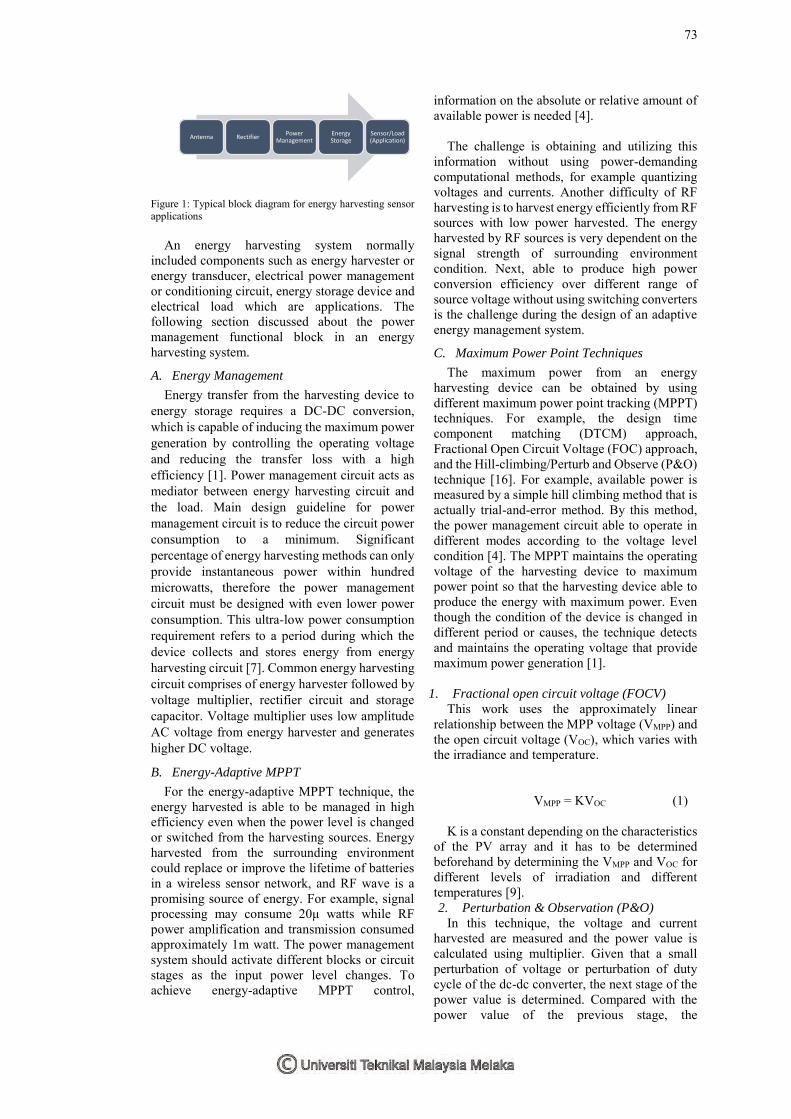
73
Figure 1: Typical block diagram for energy harvesting sensor applications
An energy harvesting system normally included components such as energy harvester or energy transducer, electrical power management or conditioning circuit, energy storage device and electrical load which are applications. The following section discussed about the power management functional block in an energy harvesting system.
A. Energy Management
Energy transfer from the harvesting device to energy storage requires a DC-DC conversion, which is capable of inducing the maximum power generation by controlling the operating voltage and reducing the transfer loss with a high efficiency [1]. Power management circuit acts as mediator between energy harvesting circuit and the load. Main design guideline for power management circuit is to reduce the circuit power consumption to a minimum. Significant percentage of energy harvesting methods can only provide instantaneous power within hundred microwatts, therefore the power management circuit must be designed with even lower power consumption. This ultra-low power consumption requirement refers to a period during which the device collects and stores energy from energy harvesting circuit [7]. Common energy harvesting circuit comprises of energy harvester followed by voltage multiplier, rectifier circuit and storage capacitor. Voltage multiplier uses low amplitude AC voltage from energy harvester and generates higher DC voltage.
B. Energy-Adaptive MPPT
For the energy-adaptive MPPT technique, the energy harvested is able to be managed in high efficiency even when the power level is changed or switched from the harvesting sources. Energy harvested from the surrounding environment could replace or improve the lifetime of batteries in a wireless sensor network, and RF wave is a promising source of energy. For example, signal processing may consume 20μ watts while RF power amplification and transmission consumed approximately 1m watt. The power management system should activate different blocks or circuit stages as the input power level changes. To achieve energy-adaptive MPPT control,
information on the absolute or relative amount of available power is needed [4].
The challenge is obtaining and utilizing this
information without using power-demanding computational methods, for example quantizing voltages and currents. Another difficulty of RF harvesting is to harvest energy efficiently from RF sources with low power harvested. The energy harvested by RF sources is very dependent on the signal strength of surrounding environment condition. Next, able to produce high power conversion efficiency over different range of source voltage without using switching converters is the challenge during the design of an adaptive energy management system.
C. Maximum Power Point Techniques
The maximum power from an energy harvesting device can be obtained by using different maximum power point tracking (MPPT) techniques. For example, the design time component matching (DTCM) approach, Fractional Open Circuit Voltage (FOC) approach, and the Hill-climbing/Perturb and Observe (P&O) technique [16]. For example, available power is measured by a simple hill climbing method that is actually trial-and-error method. By this method, the power management circuit able to operate in different modes according to the voltage level condition [4]. The MPPT maintains the operating voltage of the harvesting device to maximum power point so that the harvesting device able to produce the energy with maximum power. Even though the condition of the device is changed in different period or causes, the technique detects and maintains the operating voltage that provide maximum power generation [1].
1. Fractional open circuit voltage (FOCV)
This work uses the approximately linear relationship between the MPP voltage (VMPP) and the open circuit voltage (VOC), which varies with the irradiance and temperature.
VMPP = KVOC (1) K is a constant depending on the characteristics
of the PV array and it has to be determined beforehand by determining the VMPP and VOC for different levels of irradiation and different temperatures [9]. 2. Perturbation & Observation (P&O)
In this technique, the voltage and current harvested are measured and the power value is calculated using multiplier. Given that a small perturbation of voltage or perturbation of duty cycle of the dc-dc converter, the next stage of the power value is determined. Compared with the power value of the previous stage, the
Antenna RectifierPower
ManagementEnergy Storage
Sensor/Load (Application)
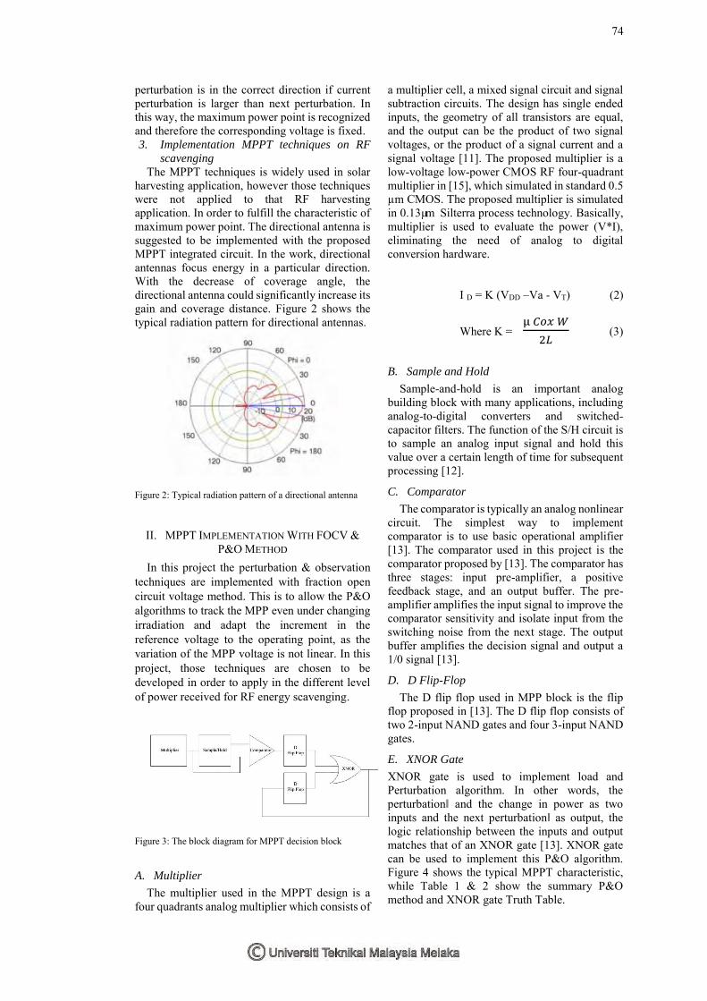
74
perturbation is in the correct direction if current perturbation is larger than next perturbation. In this way, the maximum power point is recognized and therefore the corresponding voltage is fixed. 3. Implementation MPPT techniques on RF
scavenging
The MPPT techniques is widely used in solar harvesting application, however those techniques were not applied to that RF harvesting application. In order to fulfill the characteristic of maximum power point. The directional antenna is suggested to be implemented with the proposed MPPT integrated circuit. In the work, directional antennas focus energy in a particular direction. With the decrease of coverage angle, the directional antenna could significantly increase its gain and coverage distance. Figure 2 shows the typical radiation pattern for directional antennas.
Figure 2: Typical radiation pattern of a directional antenna
II. MPPT IMPLEMENTATION WITH FOCV & P&O METHOD
In this project the perturbation & observation techniques are implemented with fraction open circuit voltage method. This is to allow the P&O algorithms to track the MPP even under changing irradiation and adapt the increment in the reference voltage to the operating point, as the variation of the MPP voltage is not linear. In this project, those techniques are chosen to be developed in order to apply in the different level of power received for RF energy scavenging.
Figure 3: The block diagram for MPPT decision block
A. Multiplier
The multiplier used in the MPPT design is a four quadrants analog multiplier which consists of
a multiplier cell, a mixed signal circuit and signal subtraction circuits. The design has single ended inputs, the geometry of all transistors are equal, and the output can be the product of two signal voltages, or the product of a signal current and a signal voltage [11]. The proposed multiplier is a low-voltage low-power CMOS RF four-quadrant multiplier in [15], which simulated in standard 0.5 µm CMOS. The proposed multiplier is simulated in 0.13µm Silterra process technology. Basically, multiplier is used to evaluate the power (V*I), eliminating the need of analog to digital conversion hardware.
I D = K (VDD –Va - VT) (2)
Where K = µ 𝐶𝑜𝑥 𝑊
2𝐿 (3)
B. Sample and Hold
Sample-and-hold is an important analog building block with many applications, including analog-to-digital converters and switched-capacitor filters. The function of the S/H circuit is to sample an analog input signal and hold this value over a certain length of time for subsequent processing [12].
C. Comparator
The comparator is typically an analog nonlinear circuit. The simplest way to implement comparator is to use basic operational amplifier [13]. The comparator used in this project is the comparator proposed by [13]. The comparator has three stages: input pre-amplifier, a positive feedback stage, and an output buffer. The pre-amplifier amplifies the input signal to improve the comparator sensitivity and isolate input from the switching noise from the next stage. The output buffer amplifies the decision signal and output a 1/0 signal [13].
D. D Flip-Flop
The D flip flop used in MPP block is the flip flop proposed in [13]. The D flip flop consists of two 2-input NAND gates and four 3-input NAND gates.
E. XNOR Gate
XNOR gate is used to implement load and Perturbation algorithm. In other words, the perturbation‖ and the change in power as two inputs and the next perturbation‖ as output, the logic relationship between the inputs and output matches that of an XNOR gate [13]. XNOR gate can be used to implement this P&O algorithm. Figure 4 shows the typical MPPT characteristic, while Table 1 & 2 show the summary P&O method and XNOR gate Truth Table.
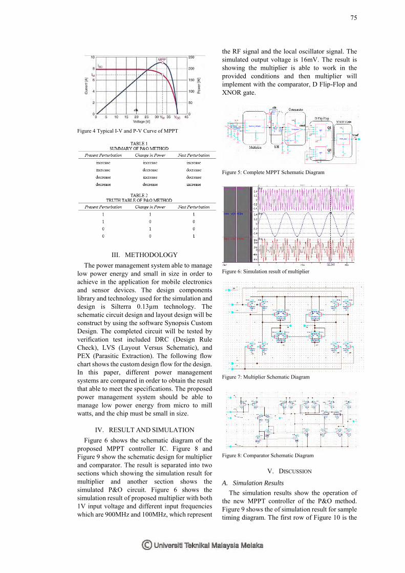
75
Figure 4 Typical I-V and P-V Curve of MPPT
III. METHODOLOGY The power management system able to manage
low power energy and small in size in order to achieve in the application for mobile electronics and sensor devices. The design components library and technology used for the simulation and design is Silterra 0.13µm technology. The schematic circuit design and layout design will be construct by using the software Synopsis Custom Design. The completed circuit will be tested by verification test included DRC (Design Rule Check), LVS (Layout Versus Schematic), and PEX (Parasitic Extraction). The following flow chart shows the custom design flow for the design. In this paper, different power management systems are compared in order to obtain the result that able to meet the specifications. The proposed power management system should be able to manage low power energy from micro to mill watts, and the chip must be small in size.
IV. RESULT AND SIMULATION Figure 6 shows the schematic diagram of the
proposed MPPT controller IC. Figure 8 and Figure 9 show the schematic design for multiplier and comparator. The result is separated into two sections which showing the simulation result for multiplier and another section shows the simulated P&O circuit. Figure 6 shows the simulation result of proposed multiplier with both 1V input voltage and different input frequencies which are 900MHz and 100MHz, which represent
the RF signal and the local oscillator signal. The simulated output voltage is 16mV. The result is showing the multiplier is able to work in the provided conditions and then multiplier will implement with the comparator, D Flip-Flop and XNOR gate.
Figure 5: Complete MPPT Schematic Diagram
Figure 6: Simulation result of multiplier
Figure 7: Multiplier Schematic Diagram
Figure 8: Comparator Schematic Diagram
V. DISCUSSION
A. Simulation Results
The simulation results show the operation of the new MPPT controller of the P&O method. Figure 9 shows the of simulation result for sample timing diagram. The first row of Figure 10 is the
clk

76
current perturbation (m-1), second row is the next perturbation (m), the third and fourth row are the clock (clk) and the comparator output (cmd). Next, the Q1 and Q2 represent the output of first flip flop and second flip flop. The timing diagram shows the operation of the proposed MPPT controller of the P&O method. As the new perturbation cycle begins at the rising edge of clock. The perturbation direction for next cycle will be determined based on the comparison results of m and m-1, where m represents the sampled result of harvested power in the present cycle and m-1 is the stored harvested power value in the last cycle. Thus, the capacitor in the storage cell will be charged (discharged). Basically, the comparator output, cmd is updated at the rising edge of clk (pulse from oscillator-clock input) and the outputs of the two flip-flops are refreshed at the rising edge of clock. If the m is greater (smaller) than m-1, the capacitor will be charged (discharged). And once its voltage is higher (lower) than m, the cmd (comparator output) will toggle and discharge/charge ends. The variation of both input for comparator will vary the cmd, which controlling the duty cycle of the whole circuit. Next, Figure 10 shows the simulation result for the Vref (XNOR gate output with energy storage) in charging state while Figure 11 shows the simulation result for discharging state.
Figure 9: Simulation results for sample timing diagram
Figure 10: Simulation result for when m is greater than m-1, the capacitor will be charged
Figure 11: Simulation result for when m is smaller than m-1, the capacitor will be discharged
VI. `CONCLUSION In conclusion, an analog MPPT power
management integrated circuit for the RF energy harvesting is proposed and simulated under Silterra 0.13µm process technology. The operation of the analog MPPT circuit has the advantage of fast and accurate tracking, miniature in size and low power consumption. The MPPT circuit able to control the charging and discharging stage by the duty cycle of the comparator output. With P&O algorithm, the duty cycle is changed or shifted according to the variation of the harvested power from transducer. The proposed MPPT circuit able to integrate with the RF energy harvesting system for mobile devices or wireless sensors.
REFERENCES [1] Heo, S., Yang, Y. S., Lee, J., Lee, S., & Kim, J. (2011).
Micro energy management for energy harvesting at maximum power point. doi:10.1109/ISICir.2011.6131896
[2] Dolgov, A., Zane, R., & Popovic, Z. (2010). Power Management System for Online Low Power RF Energy Harvesting Optimization. IEEE Transactions on Circuits
and Systems I-regular Papers. doi:10.1109/TCSI.2009.2034891.
[3] T. Paing, J. Shin, R. Zane, and Z. Popovic, “Resistor Emulation Approach to Low-Power RF Energy Harvesting,” IEEE Transactions on Power Electronics IEEE Trans. Power Electron., pp. 1494–1501.
[4] Yi, J., Su, F., Lam, Y., Ki, W., & Tsui, C. (2008). An energy-adaptive MPPT power management unit for micro-power vibration energy harvesting. doi:10.1109/ISCAS.2008.4541981.
[5] J C. Lu, C.-Y. Tsui, and W.-H. Ki, “Vibration Energy Scavenging System with Maximum Power Tracking for Micropower Applications,” IEEE Transactions on Very
Large Scale Integration (VLSI) Systems IEEE Trans. VLSI Syst., pp. 2109–2119.
[6] Maurath, D., Becker, P. F., Spreemann, D., & Manoli, Y. (2012). Efficient Energy Harvesting with Electromagnetic Energy Transducers Using Active Low-Voltage Rectification and Maximum Power Point Tracking. IEEE Journal of Solid-state Circuits. doi:10.1109/JSSC.2012.2188562.
[7] Vinko, D.; Horvat, G., "100 nA power management circuit for energy harvesting devices," in Information and Communication Technology, Electronics and
Microelectronics (MIPRO), 2014 37th International
Convention on, vol., no., pp.125-129, 26-30 May 2014 [8] Prof. Wu, “Discussion #9 MOSFET,” Spring-2008 [9] M.A.S.Mason, E.F.Fuchs, ―Theoretical and
experimental analyses of photovoltaic systems with

77
voltage and current based maximum power point tracking,‖ IEEE Trans. Energy Conv., vol. 17, no. 4, pp. 514–522, Dec. 2002
[10] G.K. Ottman et al., “Adaptive Piezoelectric Energy Harvesting Circuit for Wireless Remote Power Supply,” IEEE Trans. Power Electron. vol. 17, no. 5, Sept. 2002, pp. 669-676.
[11] K. Dejhan, P. Prommee, W. Tiamvorratat, S. Mitatha and I. Chaisayun, "A design of four-quadrant analog multiplier," Communications and Information Technology, 2004. ISCIT 2004. IEEE International
Symposium on, 2004, pp. 29-32 vol.1. doi: 10.1109/ISCIT.2004.1412443
[12] J. Cheuk Wai Wong, “CMOS Sample-and-Hold Circuits,” 2001. Department of Electrical and Computer
Engineering University of Toronto [13] W. Yi, Analog Maximum Power Point Tracking (MPPT)
IC for Solar Cells. Raleigh, North Carolina: Faculty of
North Carolina State University, 2014. [14] Zhi-Ming Lin and C. H. Huang, "A low voltage four-
quadrant CMOS analogue multiplier," Electronics,
Circuits and Systems, 1999. Proceedings of ICECS '99. The 6th IEEE International Conference on, Pafos, 1999, pp. 1333-1335 vol.3. doi: 10.1109/ICECS.1999.814415
[15] Mohammed K. Salama and Ahmed. M. Soliman, “Low-Voltage Low-Power CMOS RF Four-Quadrant Multiplier”, Int. J. Electron. Commun. (AEU) ¨ 57, No. 1, 74−78, (2003)
[16] D. Sanz Morales, Maximum Power Point Tracking Algorithms for Photovoltaic Applications. Faculty of Electronics,
Communications and Automation: Aalto
University, 2010.

78
Abstract— Energy harvesting is widely
implemented in many applications and eliminates cost to hard wire or replace batteries Through energy harvesting system, it is able to provide instantaneous power for low power electronics, wireless sensor and mobile electronics. In this paper, a power management circuit is proposed in order to control the operation stages and generate maximum power point. The control techniques use for the power management circuit is a digital Maximum Power Point Tracking (MPPT) techniques. The method that implemented in this project is perturbation and observation (P&O) algorithm, which controlled by microcontroller unit (MCU). The microcontroller unit control the condition of the buck convertor and able to operate at five operating modes according to the variations of the harvested input power and the batteries power. Thus, the microcontroller controlled the MPPT circuit by the pulse width modulation (PWM) generated by the controller.
Index Terms— Energy harvesting, MPPT, P&O, MCU, PWM.
I. INTRODUCTION everal environmental energy sources have been extensively investigated such as light, heat, vibration, and electromagnetic radiation
from communication devices. These energy sources able to provide instantaneous power for low power electronics. However, the amount of the generated energy from transducer need to manage by a regulator circuit or power management circuit. The power management system need to maintain the operating voltage of the harvesting device to maximum power output so that the harvesting device generates energy with maximum power [1]. For example, the MPPT techniques are widely used for the solar
harvesting system. The MPPT circuit usually able to control by analog circuit or control digitally. For analog MPPT circuit, the method uses an analog circuitry and a classical feedback control to create an energy scavenging system. Digital MPPT circuit uses microcontroller unit (MCU) and adaptive algorithm to track maximum power point (MPP) of the system.
A. Maximum Power Point
The maximum power from an energy harvesting device can be obtained by using different maximum power point tracking (MPPT) techniques. For example, the design time component matching (DTCM) approach, Fractional Open Circuit Voltage (FOC) approach, and the Hill-climbing/Perturb and Observe (P&O) technique [18]. For example, available power is measured by a simple hill climbing method that is actually trial-and-error method. By this method, the power management circuit able to operate in different modes according to the voltage level condition [4]. The MPPT maintains the operating voltage of the harvesting device to maximum power point so that the harvesting device able to produce the energy with maximum power. Even though the condition of the device is changed in different period or causes, the technique detects and maintains the operating voltage that provide maximum power generation [1]. Figure 1 indicates the typical power diagram for MPPT, the MPP is the maximum power output harvested while Isc is the short circuit current of the fractional short circuit current technique [18].
Digitally Controlled MPPT by Arduino Microcontroller using Perturbation and
Observation Algorithm W.P. Ang1, Y.C. Wong2
Faculty of Computer Engineering and Electronic Engineering, Universiti Teknikal Malaysia Melaka (UTeM)
Melaka, Malaysia [email protected], [email protected]
S
APPENDIX B

79
Figure 1: Typical MPPT current-voltage-power diagram
B. Perturbation & Observation (P&O)
In this technique, the voltage and current harvested are measured and the power value is calculated using multiplier. Given that a small perturbation of voltage or perturbation of duty cycle of the dc-dc converter, the next stage of the power value is determined. Compared with the power value of the previous stage, the perturbation is in the correct direction if Phase 2 is larger than Phase 1. In this way, the maximum power point is recognized and therefore the corresponding voltage is fixed.
Figure 2: Perturbation and observation algorithm flow
chart
C. Digitally Controlled MPPT
The MPPT circuit usually able to control by analog circuit or the digital circuit. For analog MPPT circuit, the method uses an analog circuitry and a classical feedback control to create an energy scavenging system. Digital MPPT circuit uses microcontroller unit (MCU) based with digital and adaptive algorithm to track MPP of the system. Compared to analog design, power consumption is the main challenge for using digital in the micro energy scavenging system. A digital MPPT circuit is constructed for this project in order to indicates the functionality and concept of the related MPPT techniques. The digital MPPT circuit is controlled by using Arduino microcontroller. The digital MPPT circuit shared the same algorithm (P&O) with the analog MPPT design of this project.
II. DIGITALCONTROLLED MPPT CIRCUIT DESIGN
In this paper, the perturbation & observation techniques are implemented with the buck convertor circuit and controlled by Arduino microcontroller. Figure 3 shows the block diagram of the digital MPPT circuit. Arduino Mega 2560 has been used in this work, and integrated with the buck converter circuit, half bridge driver, rectifier (input), energy storage and the voltage and current measurement circuit as shown in Figure 3.
Figure 3: Block diagram for digital MPPT circuit
Figure 4 shows the schematic design for the
digital MPPT circuit. The circuit excluded the voltage and current measurement block. The buck converter consists of three power MOSFET, IRFZ44N. The half bridge driver is IR2104, and energy storage is a two 1.2V rechargeable batteries. The voltage measurement is constructed by a basic voltage divider circuit while the current measurement circuit is constructed by using current sensor, MAX2473+.
Figure 4: Schematic circuit diagram for digital MPPT circuit
III. CONTROL MECHANISM IN DIGITAL MPPT Figure 5 shows the control flow chart for the
digital MPPT circuit. The digital MPPT power management circuit is controlled by the pulse width modulation (PWM) which control the direction of the energy harvester or the transducer. Firstly, the circuit will measure the voltages and currents from the input and the batteries. The analog signal will connect to the analog pins of the microcontroller and the power of both input and
Buck converter
IR2104

80
batteries will be measured. The variation of the both the input and batteries power will change or switch the operation mode of the power management circuit. Also, the microcontroller will control the PWM which control the direction of transducer according to the P&O algorithm.
Figure 5: Control mechanism for the digital MPPT circuit.
IV. OPERATION MODES OF CIRCUIT There are five operation modes for the MPPT
algorithm power management circuit where the charger modes able to switch or change the operation mode according to the conditions of input power and batteries power. The five operation modes included buck mode, float mode, sleep mode, no battery mode, discharging mode as shown in Figure 6.
A. Buck Mode
Buck mode is where the batteries start to charge by the buck circuit. The controller will send a HIGH signal to the IR2104 where the IC driver will turn on the gate of the power MOSFET to charge the batteries by the input power. The power MOSFET will be turned on, thus Enabled plotted ON and indicated on the serial monitor.
B. Float Mode Float mode is the condition when the batteries still
able to supply enough energy, after the voltage drops until the low battery level, the batteries will switch the mode “Buck” mode in order to charge the battery.
C. Sleep Mode Sleep mode is where the input voltage is in low
voltage condition where there is less supply to circuit, there will be no charging process in the mode. The circuit will turn into mode when the input voltage is less than 3V.
D. No Battery Mode No battery mode is the condition where the batteries
is removed or the batteries voltage level is drops to a
low level without charging process. The limit set for the battery voltage is 1.2V as the battery used is 2.48V.
E. Discharging Mode Discharging mode is the stage where the batteries
power is used by the load provided.
Figure 6: Operation mode under different voltage conditions
for the MPPT circuit
V. PROTOTYPE OF DIGITAL MPPT CIRCUIT AND SERIAL PRINT RESULTS
A. Prototype
Figure 7 shows the circuit constructed on breadboard, the prototype circuit contains voltage and current measurement circuits for both input and batteries, half bridge driver, buck converter, rechargeable batteries and the Arduino Mega 2560 which connected to a personal computer. However, the MPPT circuit in this project, load is not included in the circuit. Therefore, the batteries have to be discharged manually. In order to set up the measurement experiment for the power management circuit, a rectifier is connected before the power management circuit. The rectifier used is a Dickson’s Charger Pump rectifier.
Figure 7: Prototype of digital MPPT circuit
Figure 8: Measurement setup for the digital MPPT circuit
B. Serial Monitor Print and Serial Plotter Print
The prototype for digital MPPT circuit able to measure the voltages and currents for both input and batteries, therefore the powers are calculated
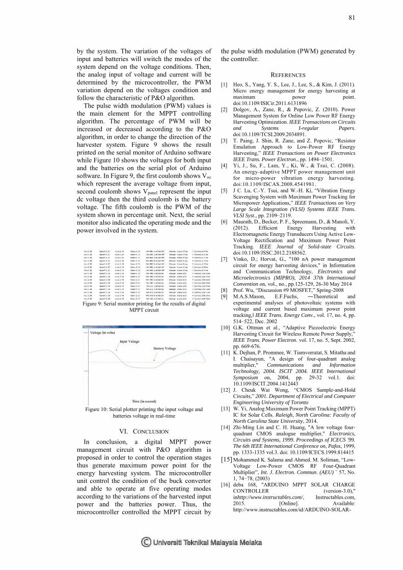
81
by the system. The variation of the voltages of input and batteries will switch the modes of the system depend on the voltage conditions. Then, the analog input of voltage and current will be determined by the microcontroller, the PWM variation depend on the voltages condition and follow the characteristic of P&O algorithm.
The pulse width modulation (PWM) values is the main element for the MPPT controlling algorithm. The percentage of PWM will be increased or decreased according to the P&O algorithm, in order to change the direction of the harvester system. Figure 9 shows the result printed on the serial monitor of Arduino software while Figure 10 shows the voltages for both input and the batteries on the serial plot of Arduino software. In Figure 9, the first coulomb shows Voc which represent the average voltage from input, second coulomb shows Vpanel represent the input dc voltage then the third coulomb is the battery voltage. The fifth coulomb is the PWM of the system shown in percentage unit. Next, the serial monitor also indicated the operating mode and the power involved in the system.
Figure 9: Serial monitor printing for the results of digital
MPPT circuit
Figure 10: Serial plotter printing the input voltage and
batteries voltage in real-time
VI. CONCLUSION In conclusion, a digital MPPT power
management circuit with P&O algorithm is proposed in order to control the operation stages thus generate maximum power point for the energy harvesting system. The microcontroller unit control the condition of the buck convertor and able to operate at five operating modes according to the variations of the harvested input power and the batteries power. Thus, the microcontroller controlled the MPPT circuit by
the pulse width modulation (PWM) generated by the controller.
REFERENCES [1] Heo, S., Yang, Y. S., Lee, J., Lee, S., & Kim, J. (2011).
Micro energy management for energy harvesting at maximum power point. doi:10.1109/ISICir.2011.6131896
[2] Dolgov, A., Zane, R., & Popovic, Z. (2010). Power Management System for Online Low Power RF Energy Harvesting Optimization. IEEE Transactions on Circuits and Systems I-regular Papers. doi:10.1109/TCSI.2009.2034891.
[3] T. Paing, J. Shin, R. Zane, and Z. Popovic, “Resistor Emulation Approach to Low-Power RF Energy Harvesting,” IEEE Transactions on Power Electronics
IEEE Trans. Power Electron., pp. 1494–1501. [4] Yi, J., Su, F., Lam, Y., Ki, W., & Tsui, C. (2008).
An energy-adaptive MPPT power management unit for micro-power vibration energy harvesting. doi:10.1109/ISCAS.2008.4541981.
[5] J C. Lu, C.-Y. Tsui, and W.-H. Ki, “Vibration Energy Scavenging System with Maximum Power Tracking for Micropower Applications,” IEEE Transactions on Very
Large Scale Integration (VLSI) Systems IEEE Trans.
VLSI Syst., pp. 2109–2119. [6] Maurath, D., Becker, P. F., Spreemann, D., & Manoli, Y.
(2012). Efficient Energy Harvesting with Electromagnetic Energy Transducers Using Active Low-Voltage Rectification and Maximum Power Point Tracking. IEEE Journal of Solid-state Circuits. doi:10.1109/JSSC.2012.2188562.
[7] Vinko, D.; Horvat, G., "100 nA power management circuit for energy harvesting devices," in Information and Communication Technology, Electronics and
Microelectronics (MIPRO), 2014 37th International
Convention on, vol., no., pp.125-129, 26-30 May 2014 [8] Prof. Wu, “Discussion #9 MOSFET,” Spring-2008 [9] M.A.S.Mason, E.F.Fuchs, ―Theoretical and
experimental analyses of photovoltaic systems with voltage and current based maximum power point tracking,‖ IEEE Trans. Energy Conv., vol. 17, no. 4, pp. 514–522, Dec. 2002
[10] G.K. Ottman et al., “Adaptive Piezoelectric Energy Harvesting Circuit for Wireless Remote Power Supply,” IEEE Trans. Power Electron. vol. 17, no. 5, Sept. 2002, pp. 669-676.
[11] K. Dejhan, P. Prommee, W. Tiamvorratat, S. Mitatha and I. Chaisayun, "A design of four-quadrant analog multiplier," Communications and Information
Technology, 2004. ISCIT 2004. IEEE International
Symposium on, 2004, pp. 29-32 vol.1. doi: 10.1109/ISCIT.2004.1412443
[12] J. Cheuk Wai Wong, “CMOS Sample-and-Hold Circuits,” 2001. Department of Electrical and Computer Engineering University of Toronto
[13] W. Yi, Analog Maximum Power Point Tracking (MPPT) IC for Solar Cells. Raleigh, North Carolina: Faculty of North Carolina State University, 2014.
[14] Zhi-Ming Lin and C. H. Huang, "A low voltage four-quadrant CMOS analogue multiplier," Electronics, Circuits and Systems, 1999. Proceedings of ICECS '99.
The 6th IEEE International Conference on, Pafos, 1999, pp. 1333-1335 vol.3. doi: 10.1109/ICECS.1999.814415
[15] Mohammed K. Salama and Ahmed. M. Soliman, “Low-Voltage Low-Power CMOS RF Four-Quadrant Multiplier”, Int. J. Electron. Commun. (AEU) ¨ 57, No. 1, 74−78, (2003)
[16] deba 168, "ARDUINO MPPT SOLAR CHARGE CONTROLLER (version-3.0)," inhttp://www.instructables.com/, Instructables.com, 2015. [Online]. Available: http://www.instructables.com/id/ARDUINO-SOLAR-

82
CHARGE-CONTROLLER-Version-30/. Accessed: May 1, 2016.
[17] Hackaday, "ARDUINO MPPT SOLAR CHARGE CONTROLLER," in hackaday.io, 2016. [Online]. Available: https://hackaday.io/project/4613/logs. Accessed: May 2, 2016.
[18] D. Sanz Morales, Maximum Power Point Tracking Algorithms for Photovoltaic Applications. Faculty of
Electronics, Communications and Automation: Aalto
University, 2010.

83
Abstract—Energy harvesting has grown from
long-established concepts into devices for powering ubiquitously deployed sensor networks and mobile electronics. An analog power management system has designed and proposed for performing maximum power point tracking (MPPT) as the fluctuation of the input power across the target frequency range. The comparator of the analog MPPT decision making block were selected to optimize and construct in this paper, the parameters of the comparator circuit has been optimized and minimized. In order to ensure accuracy result of the circuit, several layout design rules such as common centroid, interdigitated transistor, folded cascaded amplifiers are applied in the layout design of the comparator block. The integrated circuit will be simulated and designed using standard 0.13μm Silterra process technology.
Index Terms— MPPT, IC, parametric optimization, layout design, common-centroid, interdigitated transistor, folded cascaded.
I. INTRODUCTION he proposed power management circuit is an integrated circuit using analog MPPT
techniques. For analog MPPT circuit, the method uses an analog circuitry and a classical feedback control to create an energy scavenging system. The main characteristic for analog MPPT circuit is simplicity, low overhead and low cost. The devices or components used in the design must has configurable parameters. In order to meets the specifications of the circuit design, the parameters of the components such as transistors and resistors must be adjusted in order to optimize the design. For example, transistor gate width and length, or resistor dimensions can be changed to change their electrical characteristics to match the design requirements. Figure 1 shows a transistor gate width and length with resistor width and length.
Figure 1: Transistor gate width and length, or resistor In order to minimize the size of circuit design,
the size of the transistors, capacitors and other components need to be optimized. In this project the techniques use to optimize the performance of the design is using the tool, parametric analysis in the Synopsis Software. The parametric analysis tool is an interactive analysis that measures performance by simulating a circuit under varying conditions. Parametric analyses able to define one or more nested sweeps, and you can vary the value of a design variable for each sweep.
II. MPPT DECISION MAKING BLOCK The MPPT circuit usually able to control by
analog circuit or the digital control. For analog MPPT circuit, the method uses an analog circuitry and a classical feedback control to create an energy scavenging system. The main characteristic for analog MPPT circuit is simplicity, low overhead and low cost. Figure 2 is the block diagram of the MPPT decision making block.
Figure 2: The block diagram for MPPT decision block
Design and Parametric Optimization for
Comparator in MPPT Decision Making Block W.P. Ang1, Y.C. Wong2
Faculty of Computer Engineering and Electronic Engineering, Universiti Teknikal Malaysia Melaka (UTeM)
Melaka, Malaysia [email protected], [email protected]
T
APPENDIX C

84
A. Multiplier
The multiplier is used to evaluate the power (V*I), eliminating the need of analog to digital conversion hardware.
B. Sample and Hold
The function of the S/H circuit is to sample an analog input signal and hold this value over a certain length of time for subsequent processing [12].
C. Comparator
The comparator is typically an analog nonlinear circuit. The simplest way to implement comparator is to use basic operational amplifier [13]. The comparator used in this project is the comparator proposed by [13]. The comparator has three stages: input pre-amplifier, a positive feedback stage, and an output buffer. The pre-amplifier amplifies the input signal to improve the comparator sensitivity and isolate input from the switching noise from the next stage. The output buffer amplifies the decision signal and output a 1/0 signal [13].
D. D Flip-Flop
The D flip flop used in MPP block is the flip flop proposed in [13]. The D flip flop consists of two 2-input NAND gates and four 3-input NAND gates.
E. XNOR Gate
XNOR gate is used to implement load and Perturbation algorithm. In other words, the perturbation‖ and the change in power as two inputs and the next perturbation‖ as output, the logic relationship between the inputs and output matches that of an XNOR gate [13].
III. METHODOLOGY The power management system able to manage
low power energy and small in size in order to achieve in the application for mobile electronics and sensor devices. The technology used for the simulation and design is CMOS 0.13µm technology. The schematic circuit design and layout design will be construct by using the software, Synopsis Custom Design. Then, the completed layout design will be tested by verification test included DRC (Design Rule Check), LVS (Layout Versus Schematic), and PEX (Parasitic Extraction). The following flow chart shows the custom design flow for the design. The accuracy of the circuit is important; thus the layout design need to be designed according to the layout design rules in order to ensure accurate results.
Figure 3: Flow chart for custom design process
IV. PARAMETRIC OPTIMIZATION In order to minimize the size of the power
management circuit design, the size of the transistors, capacitors and other components need to be optimized. In this project the techniques use to optimize the performance of the design by using parametric analysis sweeping tool in the Synopsis. Figure 7 indicates the schematic diagram with labelled transistor and finalized parameters, the transistors labelled as M1 to M12 is pmos transistor while transistors M13 to M19 is nmos transistor. Next, the first parameter to be analyzed is the length of the pmos transistor (Lp), the parameter sweeps from 0.5µm until 15µm with 8 step point for the whole analysis. The simulation result for parametric analysis for Lp is shown in Figure 4 and Figure 5, which are the zoomed in diagram and the diagram in smaller scale.
Figure 4: Parametric analysis for Lp sweep from 0.5µm to
15µm
Figure 5: Parametric analysis for Lp (small scale)
The variation for the output of comparator by

85
sweeping the parameter Lp is actually is low. Therefore, the parameter for Lp is set as low as possible in order to reduce the total sizing for the comparator. Next, the width W is analyzed, the width for both pmos (Wp) and nmos (Wn) shared the same value for the comparator, as a result the widths will be analyzed by using the same variable value. The width of the transistor is sweep from 0.5µm to 20µm with 8 step points in order to observe the variation for the increasing width. Figure 6 shows the parametric analysis for the width parameter. It is found that the smaller width will actually maintain more constant output for the comparator. The first line of the graph is actually representing the 0.5µm condition, then same goes to following defined width values.
Figure 6: Parametric analysis for comparator circuit width
seep from 0.15µm to 20µm
After the parametric analysis, the width and the length for the transistor is defined. The length of each pmos transistors, Lp are set to 0.16 µm while nmos Ln is 0.13µm. Only for the transistor M9 and M10 (pmos) set the length is set to 0.13µm. The lengths of M9 and M10 is set as the ratio of the comparator of [13].
Figure 7: Schematic of comparator of analog MPPT circuit
V. LAYOUT DESIGN In the Layout design process, the components
presenting in schematic are place in the new cell view for layout, and the circuit is connecting to each other according to schematic. During the path connection, designer have to ensure that layout will not affect circuit operation. Also, ensure that layout does not violate fabrication rules. The aim of layout design is to lay out a physical view of the schematic, which will
operate the same way. In order to prevent parasitic effect and maintain the circuit performance, several layout design rules need to be considered, this section will discuss the basic design rules of layout design.
A. Matching Single Transistor
A CMOS transistor basically crossed with two rectangles, polysilicon and active area. Each transistor of the design should be arranged in same orientation for the layout design as the current for the circuit flowing in the same direction.
B. Multiple Fingers
Multiple fingers layout design is more preferable to reduce parasitic capacitance and the resistance. By divide the transistor into multiple fingers also able to split the layout area in order to fulfill design requirement
C. Interdigitated devices
The interdigitated pattern used for the layout design for the comparator is a four finger design, with pattern ABBA.
Figure 8: Typical circuit use for interdigitated transistor
pairs
Figure 9: Interdigitated transistor pattern
D. Dummy
The dummy pattern may be formed to reduce the production tolerance. It is important to maintain the same environment on the two side of the axis symmetry, the dummy happened when one metal line passing over only one of the transistor indeed degrade the symmetry and increasing the mismatch. The path need to be connected as both ends of the same drains or sources connection.
E. Common Centroid
The common centroid pattern used for the layout design is a cross coupling design as shown in Figure 4.
Wp = Wn = 0.65µm Lp = 0.16µm Ln = 0.13µm

86
Figure 10: Typical circuit for common centroid transistor
pairs
Figure 11: Common centroid pattern
F. Folded Cascade Amplifier
The folded cascade amplifier compiles the interdigitated pattern, common-centroid pattern, dummy and other design rule to form a complete circuit layout. Figure 12 indicate a draft layout arrangement and allocation for each transistor and transistors set before the layout design in the software. This is to make sure the layout arrangement before designing true layout. D1 and S1 represent the drain and source for transistor M1 from Figure 7, same configuration for the rest of the transistors.
Figure 12: Allocation draft for comparator circuit layout
design with schematic design
After the allocation confirmed, the layout is design in the Synopsis software. Figure 13 shows the allocation and arrangement of the transistor in the software while Figure 14 shows the complete layout design for the comparator of analog MPPT power management circuit.
Figure 13: Allocation and arrangement of the transistor in the
software
Figure 14: Complete layout design for the comparator of
analog MPPT power management circuit
VI. CONCLUSION In conclusion, the comparator of proposed
analog MPPT circuit were selected to optimize the parameters of the circuit. The parameters of the comparator circuit have been optimized and the size of the circuit has minimized. Moreover, in order to ensure accuracy result of the circuit, several layout design rules such as common centroid, interdigitated transistor, folded cascaded amplifiers are applied in the layout design of the comparator block.
REFERENCES [1] Heo, S., Yang, Y. S., Lee, J., Lee, S., & Kim, J. (2011).
Micro energy management for energy harvesting at maximum power point. doi:10.1109/ISICir.2011.6131896
[2] Dolgov, A., Zane, R., & Popovic, Z. (2010). Power Management System for Online Low Power RF Energy Harvesting Optimization. IEEE Transactions on Circuits
and Systems I-regular Papers. doi:10.1109/TCSI.2009.2034891.
[3] T. Paing, J. Shin, R. Zane, and Z. Popovic, “Resistor Emulation Approach to Low-Power RF Energy Harvesting,” IEEE Transactions on Power Electronics IEEE Trans. Power Electron., pp. 1494–1501.
[4] Yi, J., Su, F., Lam, Y., Ki, W., & Tsui, C. (2008). An energy-adaptive MPPT power management unit for micro-power vibration energy harvesting. doi:10.1109/ISCAS.2008.4541981.
[5] J C. Lu, C.-Y. Tsui, and W.-H. Ki, “Vibration Energy Scavenging System with Maximum Power Tracking for Micropower Applications,” IEEE Transactions on Very
Large Scale Integration (VLSI) Systems IEEE Trans. VLSI Syst., pp. 2109–2119.
[6] Maurath, D., Becker, P. F., Spreemann, D., & Manoli, Y. (2012). Efficient Energy Harvesting with Electromagnetic Energy Transducers Using Active Low-

87
Voltage Rectification and Maximum Power Point Tracking. IEEE Journal of Solid-state Circuits. doi:10.1109/JSSC.2012.2188562.
[7] Vinko, D.; Horvat, G., "100 nA power management circuit for energy harvesting devices," in Information and Communication Technology, Electronics and
Microelectronics (MIPRO), 2014 37th International Convention on, vol., no., pp.125-129, 26-30 May 2014
[8] Prof. Wu, “Discussion #9 MOSFET,” Spring-2008 [9] M.A.S.Mason, E.F.Fuchs, ―Theoretical and
experimental analyses of photovoltaic systems with voltage and current based maximum power point tracking,‖ IEEE Trans. Energy Conv., vol. 17, no. 4, pp. 514–522, Dec. 2002
[10] G.K. Ottman et al., “Adaptive Piezoelectric Energy Harvesting Circuit for Wireless Remote Power Supply,” IEEE Trans. Power Electron. vol. 17, no. 5, Sept. 2002, pp. 669-676.
[11] K. Dejhan, P. Prommee, W. Tiamvorratat, S. Mitatha and I. Chaisayun, "A design of four-quadrant analog multiplier," Communications and Information
Technology, 2004. ISCIT 2004. IEEE International Symposium on, 2004, pp. 29-32 vol.1. doi: 10.1109/ISCIT.2004.1412443
[12] J. Cheuk Wai Wong, “CMOS Sample-and-Hold Circuits,” 2001. Department of Electrical and Computer
Engineering University of Toronto
[13] W. Yi, Analog Maximum Power Point Tracking (MPPT) IC for Solar Cells. Raleigh, North Carolina: Faculty of
North Carolina State University, 2014. [14] Zhi-Ming Lin and C. H. Huang, "A low voltage four-
quadrant CMOS analogue multiplier," Electronics,
Circuits and Systems, 1999. Proceedings of ICECS '99.
The 6th IEEE International Conference on, Pafos, 1999, pp. 1333-1335 vol.3. doi: 10.1109/ICECS.1999.814415
[15] Mohammed K. Salama and Ahmed. M. Soliman, “Low-Voltage Low-Power CMOS RF Four-Quadrant Multiplier”, Int. J. Electron. Commun. (AEU) ¨ 57, No. 1, 74−78, (2003)
[16] F. Malobeti, "Transistor and Basic Cell Layout Part2," in Layout of Analog CMOS Integrated Circuit.
[17] A. Kitagawa, "Analog layout design,". Microelectronics Research Lab.: Kanazawa University.

88
APPENDIX D
89
APPENDIX E