
AdamCarroll-X00104026-Semester4Report
39
Adam Carroll Semester 4 Report X00104026 HIGHER CERTIFICATE IN ELECTRONIC ENGINEERING ACADEMIC YEAR 2013/2014 Department of Electronic Engineering Project title: Analogue to Digital Converter (Semester 4) Student name: Adam Carroll Student ID: X00104026 Submission date: 09/05/2014 Supervisor: Tom Murray 1 | Page
-
Upload
adam-carroll -
Category
Documents
-
view
12 -
download
0
Transcript of AdamCarroll-X00104026-Semester4Report

Adam Carroll Semester 4 Report X00104026
HIGHER CERTIFICATE IN ELECTRONIC ENGINEERING
ACADEMIC YEAR 2013/2014
Department of Electronic Engineering
Project title: Analogue to Digital Converter (Semester 4)
Student name: Adam Carroll
Student ID: X00104026
Submission date: 09/05/2014
Supervisor: Tom Murray
1 | P a g e

Adam Carroll Semester 4 Report X00104026
Declaration
This project entitled “Digital to Analogue Converter” is my original work and has not been submitted
for any other purpose to any other institute.
Signed: ........................................................
Full Name: .......................................................
Student No: ........................................................
Acknowledgements
Tom Murray was the lecturer for the digital to analogue converted, a thanks is owed to him for his
support and assistance during this project. I would also like to thank my classmates. Doing the same
project was very helpful because everyone in the class was more than willing to help if anybody was
unsure or had a question to ask, which was most helpful.
2 | P a g e

Adam Carroll Semester 4 Report X00104026
ContentsChapter 1 – Project Plan........................................................................................................................4
Chapter 2 – Abstract..............................................................................................................................5
Chapter 3 – Introduction.......................................................................................................................5
Chapter 4 – PCB Design.........................................................................................................................6
Chapter 5 – Arduino Code Introduction..............................................................................................12
i. Serial Communication..............................................................................................................12
ii. Analogue to Digital Conversion................................................................................................13
iii. Test Connections.....................................................................................................................13
Chapter 6 – Surface Mount Technology (SMT)....................................................................................16
Chapter 7 – Fault Finding.....................................................................................................................19
Chapter 8 – LM35 Temperature Sensor...............................................................................................21
Chapter 9 – Measuring Temperature..................................................................................................23
Chapter 10 – Writing Temperature to LCD using Uno32.....................................................................24
Chapter 11 – Bill of Materials..............................................................................................................27
Chapter 12 – Equipment Used.............................................................................................................28
Chapter 13 – Environmental Factors...................................................................................................28
Chapter 14 – Conclusion......................................................................................................................29
3 | P a g e

Adam Carroll Semester 4 Report X00104026
Chapter 1 – Project Plan
Report WritingStart: Fri 02/05/14ID: 5Finish: Fri 09/05/14Dur: 6 daysRes:
Multisim & UltiboardStart: Fri 07/02/14ID: 1Finish: Fri 28/02/14Dur: 16 daysRes:
Arduino Code WritingStart: Fri 07/03/14ID: 2Finish: Fri 21/03/14Dur: 11 daysRes:
Soldering & TestingStart: Fri 28/03/14ID: 3Finish: Fri 11/04/14Dur: 11 daysRes:
Faulting FindingStart: Fri 18/04/14ID: 4Finish: Fri 25/04/14Dur: 6 daysRes:
4 | P a g e

Adam Carroll Semester 4 Report X00104026
Chapter 2 – Abstract
The aim of this project was to build a digital to analogue converter over the semester 4 of year 2. In
the class the aim was to build on your knowledge of different aspects of the course. Varying from
designing a PCD for manufacture using Multisim & Ultiboard, writing code on new software called
Mpide and learning how to solder micro components such as chips and resistors. The focus of the
project was broken into several parts;
I. Design
II. Writing code
III. Soldering practice.
At the start of the class you would talk about the tasks in hand with Tom and carry these tasks out.
Over the 12 week semester each of the skills mentioned above would be significantly improved as
they were vital to the project working. Over the twelve weeks a successful working board was
achieved by most and overall skills were significantly improved.
Chapter 3 – Introduction
The aim of this project was to have a properly functioning digital to analogue circuit PCB with the use
of an Uno32 Arduino board. One that would be able to take it temperature of its surroundings and
display it on the 40 pin LCD. This would be done through the Mpide software where you write a code,
transfer it to the Uno32 Arduino board through serial communication. Then the code that was written,
if correct, would transfer this data to the LCD. It is an exciting prospect to be able to get the chance to
design and build your very own project, as this is a vital skill that an engineer has to maintain. As
mentioned in the semester 3, this project was to be very challenging at times, but, a lot of the skills we
gained, such as micro soldering for example, something that would not have been covered before. It
also gave an insight into industry where PCB’s are designed and manufactured every day using
particular types of material and processes
Other sides of industry were also explored as there was introduction to SMT (Surface Mount
Technology) which is of standard regulation, compared to previous lectures the student would only
have experience soldering components that were two or three times as big.
When a PCB came back from production it had to be tested and trailed to discover if it had errors.
This is another vital skill that an engineer has to have a problem solving is sometimes depending on
the job something that occurs on a daily basis.
5 | P a g e
Adam Carroll Semester 4 Report X00104026
Chapter 4 – PCB Design
Mentioned in the first class by Tom Murray (class project lecturer) this semester of the project would
require less physical building than the last. The three main characteristics of this project semester
would be;
I. Design
II. Writing code
III. Soldering practice.
From the board composed in semester 3 the only components that would be required this time would
be the three decoders (74HCT4543) and the physical LCD from the actual project. The reason for this
being that a code could be written in the Mpide software and transferred to the PCB through the Uo32
Arduino board. This meant that these components would no longer be necessary.
The next part was to then begin the design of the board. As mentioned above, the three decoders
(74HCT4543) and the LCD from the semester 3 project would be the only components necessary this
semester. A PCB would have to be designed from scratch that carried out the same function as the
previous board but at a fraction of the physical size. It was decided that the Multisim & Ultiboard
software would be the software that would be used for this project.
When designing the board it was becoming difficult to place connections, this was due to the lack of
space of the page, so in order to get around this a data bus was required. It was advised by Tom to
use a data bus. A data bus is a computer subsystem that allows for the transferring of data from one
component to another on a motherboard. This would allow for multiple connections going to a similar
or different component to travel on the same track. This would save a lot of space, something that
was becoming increasingly smaller with the more tracks were placed. It would turn out to be extremely
helpful as the project progressed. Figure.1 shows the difference bewteen a data bus & 3 connections.
Figure.1
The data buses used in this project were called DataBus, CTRLBus & DisplayBus. The address (data)
inputs that were connected to DataBus were D0-D3 which were connected to digital I/O pin J4. The
address (data) inputs that were connected to CTRLBus were Enable (EN), Blank (BL) & Phase (PH)
which were connected to the power pin J1, the digital I/O pins J3 & J4 and also the LCD. The
6 | P a g e

Adam Carroll Semester 4 Report X00104026
segment outputs were on the DisplayBus which were primarily connected to the LCD but also to the
digital I/0 pin J3.
After making the respective connections from the decoders to the LCD a power supply had to be
designed which would drive these three decoder chips. This would be J1 on the PCB board (but is J2
on the Uno32, which it would eventually be connected to down the line). This project required three
ports from J1, a 5V power supply and two common GND’s. Resistor R1 would be used as a pull-up
resistor for when the board was set to 5V DC, which meant that all components had a voltage/current
flowing through them. R1 was connected to three capacitors C1, C2 & C3, these capacitors would
eliminate any noise that was present. These three capacitors were connected to R2, which was a pull-
down resistor that would pull the board to GND when the board was set to 0V DC. Figure.2 as shown
below is simply a voltage divider where the output is connected to port A0 on J2 on the PCB (or
Analog I/P J2, port A0 also).
Figure.2
After I had made all the required connections in Multisim, this part of the design was now complete.
The final design can be shown below in Figure.3
Figure.3
7 | P a g e

Adam Carroll Semester 4 Report X00104026
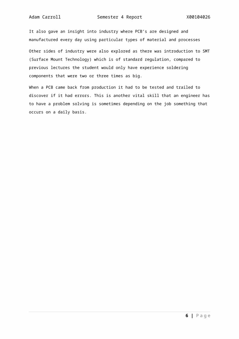
After the Multisim part of the design was complete it was then time to transfer the design to Multisim.
But just before the design could be transferred, each of the components had to be given a footprint.
For the LCD a separate footprint had to be created. The whole Multisim design is then ready to be
transferred to Ultiboard, the transferred design, Figure. 4 is shown below.
Figure.4
Next, was to make all of the connections that had been laid down in Multisim and replicate this in the
Ultiboard using the ‘follow me’ track placing function command which highlights the tracks made in
Multisim. There is a function called auto-route, which gives you an option to automatically place the
tracks but this was option was not chosen for this project. After several attempts at trying this auto-
route function the program froze due to the lack of room available. Manually rooting was then chosen
as the designer had a big say in the layout of the PCD.
Placing each track individually is quite time consuming but the user is ensured a genuine connection
will be made in the correct place. Also the error rate for this would turn out to be quite low compared
to those who used the ‘auto-route’ function. After all the tracks had been manually placed there was
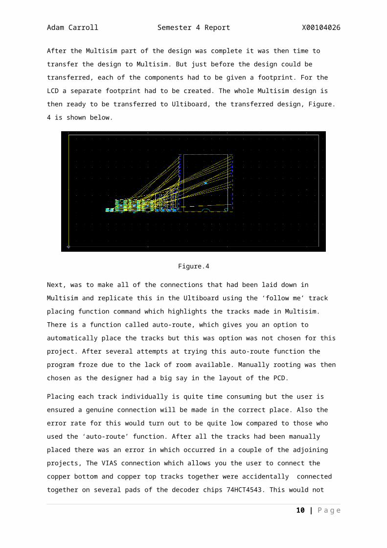
an error in which occurred in a couple of the adjoining projects, The VIAS connection which allows
you the user to connect the copper bottom and copper top tracks together were accidentally
connected together on several pads of the decoder chips 74HCT4543. This would not ensure a 100%
connection, 50/50 or the “toss of a coin” was the best description of its possible functionality. A picture
of a vias is shown below in Figure.5
Figure.5
8 | P a g e

Adam Carroll Semester 4 Report X00104026
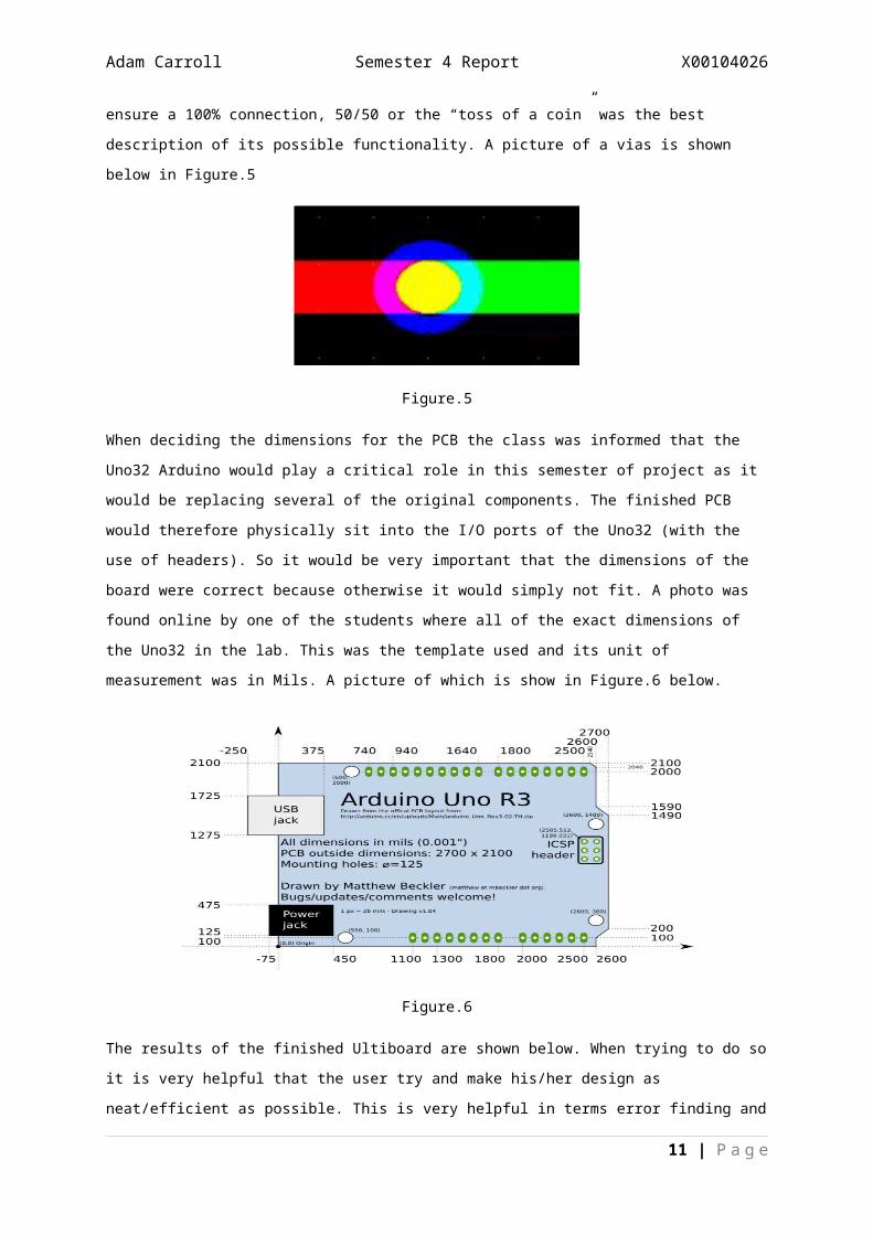
When deciding the dimensions for the PCB the class was informed that the Uno32 Arduino would play
a critical role in this semester of project as it would be replacing several of the original components.
The finished PCB would therefore physically sit into the I/O ports of the Uno32 (with the use of
headers). So it would be very important that the dimensions of the board were correct because
otherwise it would simply not fit. A photo was found online by one of the students where all of the
exact dimensions of the Uno32 in the lab. This was the template used and its unit of measurement
was in Mils. A picture of which is show in Figure.6 below.
Figure.6
The results of the finished Ultiboard are shown below. When trying to do so it is very helpful that the
user try and make his/her design as neat/efficient as possible. This is very helpful in terms error
finding and especially in terms of a visual aspect. Nobody likes to look at a PCB that has tracks here,
there and everywhere. There is a definite room for improvement in this respect. Figure.7 below shows
the finished Ultiboard design.
Figure.7
9 | P a g e
Adam Carroll Semester 4 Report X00104026
RF-4 (RF meaning Retardant Flame) is the primary insulating backbone upon which the vast majority
of rigid PCB’s are produced. A thin layer of copper foil is laminated to one, or both sides of an FR-4
glass epoxy panel. These are commonly referred to as copper clad laminates. It is the primary
insulating backbone upon which the vast majority of PCB’s are produced. The RF-4 copper clad
sheets are fabricated with circuitry engraved into copper layers to produce the PCB’s. Figure.8 below
shows a RF- 4 board.
Figure.8
Source of information about the: RF-4 – https://en.wikipedia.org
10 | P a g e
Adam Carroll Semester 4 Report X00104026
Chapter 5 – Arduino Code Introduction
Once the boards were sent away for production it was time to practice writing code with the Mpide
software as mentioned before. There was an introduction to the basic software of the Uno32 where
topics such as writing code for analogue to digital conversion, serial communication and test
connections were covered. All of which are discussed and shown below.
i. Serial Communication – The Uno32 board has two hardware serial ports. One of
these is used to create an USB interface that allows the MPIDE software to communicate with
the Uno32 board through an USB port. This will allow for a two-way serial communication
between the Uno32 and the PC. The Uno32 board receives a serial command through the
PC’s USB port to carry out a specific code which will print digits on the LCD. In return, the
Uno32 board acknowledges to the PC by sending the new state of the LED. The code is as
shown in Figure.9
Figure.10
11 | P a g e

Adam Carroll Semester 4 Report X00104026
ii. Analogue to Digital Conversion –
The LM35 is a temperature sensor that provides an analog output voltage which is linearly
proportional to the Celsius temperature. It does not require any external adjustment and is
rated to operate over -55°C to 150°C. The temperature-to-voltage conversion factor is
32mV/°C. This means it gives an output of 320 mV at 10°C temperature. The LM35 output is
connected to analog I/P channel A0 port J7 of Uno32 for ADC conversions. The ADC output
derives the temperature information, which is later displayed on the LCD. The code is as
shown in Figure.11
Figure.11
iii. Test Connections –
Digital inputs are useful to determine whether there is a connection between different test pins
on the PCB. A simple application of digital input is writing to a particular pin, setting it high for
one second and the setting it low for another second. Which will show something similar to a
square wave when you scope the test pin, meaning that there is a connection on that in. The
state is continuously switching by one second and this is read by Uno32, which will flash the
LED on and off every time the switch is pressed. The code is as shown in Figure.12
12 | P a g e
Adam Carroll Semester 4 Report X00104026
Figure.12
Figure.13 as shown below shows all of the physical I/O connections on the Uno32 and the project I/O
pins of which will be sitting into them. Note that the project pins were labelled J1-J4 and the Uno32
has its own set J pin numbers.
13 | P a g e
J1 / J2Reset3V35V0GNDGNDVINJ2 / J7A0 A6A1 A7A2 A8A3 A9A4 A10A5 A11
J3 / J5AKP13 Phase/ComP12 ColP11 DotP10 BlankP9 EN3/KP8 EN2J4 / J6P7 EN1P6 EN0P5 D3P4 D2P3 D1P2 D0P1 TxP0 Rx

Adam Carroll Semester 4 Report X00104026
Figure.13
*J1, the purple writing represents the port location J1 on the PCB.
J2 in red writing represents the port location J2 on the Uno32*
It is also worth noting what each of these ports do:
= USB Serial Communication to PC
= Data Bus for display
= Enables for each decoder
14 | P a g e
P1 Tx
P0 Rx
P5 D3
P4 D2
P3 D1
P2 D0
P9 EN3/K
P8 EN2
P7 EN1
P6 EN0
A
K
P13 Phase/Com
P12 Col
P11 Dot
P10 Blank

Adam Carroll Semester 4 Report X00104026
= The output pins, that will travel to the LCD
Figure.14 below shows all of the pins of the LCD but for this the primary concern is the Phase, Col,
Dot & Blank pins.
Figure.14
Chapter 6 – Surface Mount Technology (SMT)
While the boards were sent away the Mpide software was used and there was also an introduction to
Surface Mount Technology (SMT).
Abbreviated as SMT, surface mount technology is a design standard for constructing
electronic circuits where the components are mounted directly onto the surface of the printed circuit
board (PCB). The components have small metal tabs (or caps) that are soldered directly to the
surface of the printed circuit board on tin-lead, silver, or gold plated copper pads, called solder pads.
In the case of this project the pads were gold plated copper.
In industry it has largely replaced through-hole technology, which is the method of soldering
components with wire leads into a hole a PCB. Surface mount components are generally smaller than
through-hole parts because they either have smaller leads or no leads at all.
For this project the user would have to solder the components onto the board once the board came
back from production. There was decision to be made regarding this, the user would have a choice of
either soldering the components on by hand or use an alternative method where the board would be
placed into an oven. You would be given a solder mask, place it over the board and would scrap the
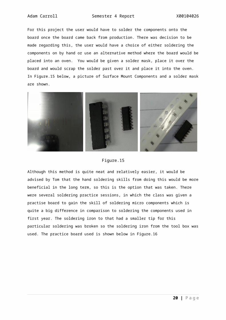
solder past over it and place it into the oven. In Figure.15 below, a picture of Surface Mount
Components and a solder mask are shown.
15 | P a g e

Adam Carroll Semester 4 Report X00104026
Figure.15
Although this method is quite neat and relatively easier, it would be advised by Tom that the hand
soldering skills from doing this would be more beneficial in the long term, so this is the option that was
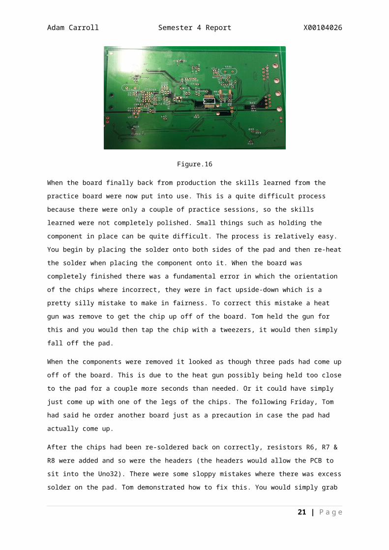
taken. There were several soldering practice sessions, in which the class was given a practise board
to gain the skill of soldering micro components which is quite a big difference in comparison to
soldering the components used in first year. The soldering iron to that had a smaller tip for this
particular soldering was broken so the soldering iron from the tool box was used. The practice board
used is shown below in Figure.16
Figure.16
When the board finally back from production the skills learned from the practice board were now put
into use. This is a quite difficult process because there were only a couple of practice sessions, so the
skills learned were not completely polished. Small things such as holding the component in place can
be quite difficult. The process is relatively easy. You begin by placing the solder onto both sides of the
pad and then re-heat the solder when placing the component onto it. When the board was completely
finished there was a fundamental error in which the orientation of the chips where incorrect, they were
in fact upside-down which is a pretty silly mistake to make in fairness. To correct this mistake a heat
gun was remove to get the chip up off of the board. Tom held the gun for this and you would then tap
the chip with a tweezers, it would then simply fall off the pad.
16 | P a g e

Adam Carroll Semester 4 Report X00104026
When the components were removed it looked as though three pads had come up off of the board.
This is due to the heat gun possibly being held too close to the pad for a couple more seconds than
needed. Or it could have simply just come up with one of the legs of the chips. The following Friday,
Tom had said he order another board just as a precaution in case the pad had actually come up.
After the chips had been re-soldered back on correctly, resistors R6, R7 & R8 were added and so
were the headers (the headers would allow the PCB to sit into the Uno32). There were some sloppy
mistakes where there was excess solder on the pad. Tom demonstrated how to fix this. You would
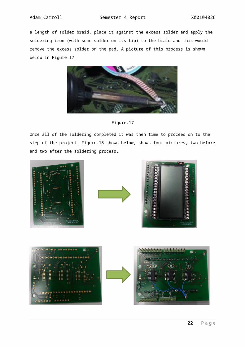
simply grab a length of solder braid, place it against the excess solder and apply the soldering iron
(with some solder on its tip) to the braid and this would remove the excess solder on the pad. A
picture of this process is shown below in Figure.17
Figure.17
Once all of the soldering completed it was then time to proceed on to the step of the project. Figure.18
shown below, shows four pictures, two before and two after the soldering process.
17 | P a g e

Adam Carroll Semester 4 Report X00104026
Figure.18
18 | P a g e

Adam Carroll Semester 4 Report X00104026
Chapter 7 – Fault Finding
As shown in Firgure.18 above, all of the components were now soldered onto the board so it was
now time to test the board. This is done by connecting the PCB onto the Uno32 and using the code
shown in Figure.12 called ‘TestConnection_V2’. This code would test each individual Test pins from
1-8 and then have to scope this and it would produce a square wave on the designated pin.
Figure.19 below shows the output on Test Pin2.
Firgure.19
This showed that each of the test pins 1-8 were all working correctly. Next was the hardware test.
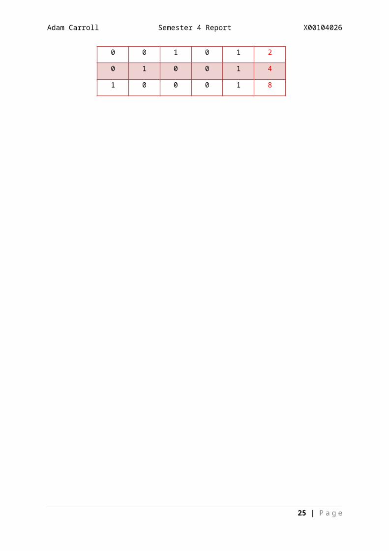
J4 P5 P4 P3 P2 P6
D3 D2 D1 D0 EN0 Output
0 0 0 0 1 0
0 0 0 1 1 1
0 0 1 0 1 2
0 1 0 0 1 4
1 0 0 0 1 8
19 | P a g e
Adam Carroll Semester 4 Report X00104026
If all the conditions are met as follows, this data should transfer from the Uno32, through to the
headers, then to the 74HCT4535 decoder chips and finally to the LCD, displaying whichever binary
number has been selected in the code. The results of this showed that the board was not working
because the display was completely blank. The next step was to begin fault finding, this showed that
there were 4 errors on this board.
1) Forgot to make a solder splash for resistor R2 – Because there was no solder splash it meant
that the resistor R2 that was the pull-down resistor was not supplying Ground (GND) to the
decoders (U1, U2 & U3).
2) Forgot to make a solder splash for resistor R1 – Because there was no solder splash it meant
that the resistor R1 that was a pull-up resistor was not supplying 5V (VCC) to the decoders
(U1,U2 & U3).
3) Missing a GND rail for the decoders (U1, U2 & U3) – To fix this Pin 8 of the decoders (GND
Pin) was soldered to R2 meaning they now had GND to drive the LCD.
4) Used the 3V3 header port on J1 – The board had a 3V3 supply flowing through it, this was
incorrect because you needed a %v supply. To fix this there was a solder splash between the
3V3 header and 5V header and cut the 3V3 header off so that it would not be directly
connected to the Uno32.
20 | P a g e
Adam Carroll Semester 4 Report X00104026
Chapter 8 – LM35 Temperature Sensor
The LM35 is an integrated circuit temperature sensor that has an output voltage linearly proportional to centigrade temperature.
Features:
Reads temperature in Celsius(°C0 OR Centigrade Its range varies from roughly -55°C to +150°C Low costing due to the wafer-level trimming It operates from 4V to 30V Less than 60µA current drain It is suitable for remote applications, which is what this project is
The code in Figure.20 below shows the code that coverts the analog voltage to a temperature below. The voltage value for this is voltage = value*32mV and if the value is greater than 1.72 (value>1.72), temperature is found by multiplying the value (which is greater than 1.72 because it has jumped down to the next line of code) by 100/1024 = 0.097655625 = Temperature
The second picture below shows the temperature of the surrounding. When the code is verified and uploaded you click the serial monitor button which will show the temperature.
Figure.20 below shows the Mpide functions verify, upload and serial monitor, the code used in configuring temperature (taken from ‘Write_Temperature_to_LCD’ code) & the result through the serial monitor.
Figure.20
21 | P a g e
Adam Carroll Semester 4 Report X00104026
It is also worth noting that a small test can be carried to test you temperature sensor. Pinch the sides of it, this will result in an increase in temperature. If this gain in temperature is shown the sensor through the serial monitor is working correctly.
Figure.21
Figure.21 Above shows the physical look of the LM35, showing where each of the pins goes into J5,
the voltage divider. Figure.22 below shows where each pin will go.
Figure.22
BE CAREFUL! – When placing the temperature sensor into J5 because if it is placed in the wrong
way it will overheat and the entire component will burn out.
22 | P a g e

Adam Carroll Semester 4 Report X00104026
Chapter 9 – Measuring Temperature
Figure.23 below shows two temperature codes. Version 1 is on the left and Version 2, on the right.
Version 1 of this code is relatively simple where it takes in a reading from the temperature sensor and
displaying it on the serial monitor. Version 2 is a bit more complicated where this time you are writing
for the temperature to be display on the LCD.
This was done by the introduction of int’s or integers. Which will write to Dig0 = temp%1, Dig1 = temp
%10, Dig2 = temp%100 & Dig3 = temp%1000. A similar instruction to ‘Write_Temperature_to_LCD’
will now happen here where the analog voltage is read from the temperature sensor and then
converted by using the following line of code - ((100*Sample)*5)/1024 which when calculated will be:
= AnalogueVoltage
1024=Answer x SampleValue
Firgure.23
23 | P a g e

Adam Carroll Semester 4 Report X00104026
Chapter 10 – Writing Temperature to LCD using Uno32
After carrying out the whole process of the design, testing and code writing it was now time to carry
out the last step in the project. The user needed to write a piece of code which would be able to
display the temperature of its surroundings and display it clearly on the LCD. First a code had to be
assembled where you could communicate to the LCD through the Uno32 board. This was a relatively
simply code to write. First you would activate the following pins 2,3,4,5,6,7,8,10,13. You do this simply
by declaring it ‘ pinMode(2,OUTPUT); ’ this would then activate pin 2 and whatever other pin that has
been declared. You then assign a value of 2 to an integer called pin. If the value of pin is less than 8,
you keep incrementing it until it is less than or equal to it. As shown:
‘ (int pin=2;pin <=8;pin++) ‘
You then declare the digital pin to a Logic ‘1’ or 5V so the pin can be activated high. You then write to
each of the digits on the LCD, this should display all zeros on the output ([000]). This is a handy piece
of code for communicating to the board. Shown:
After this code had been completed the user now knew that communication was possible between the
program and the LCD, and that printing temperature was not too far away.
24 | P a g e
digitalWrite(pin,HIGH);{
}
digitalWrite(6,LOW);
digitalWrite(7,LOW);
digitalWrite(8,LOW);
Adam Carroll Semester 4 Report X00104026
Next what had to be done was the final piece of code which is shown Figure.24 below. This will also
be described below, paragraph by paragraph because it is quite long.
Figure.24
The first paragraph of the code simply tells the LCD the different binary combinations varying from
Decimal 0 [0,0,0,0] to Decimal 9 [1,0,0,1] and also Blank [1,1,1,1]. The next paragraph simply
declared all of that outputs on the Uno32 pins 2-13 which made them available to be written to. The
next step is the ADC code/ formula, which, as mentioned before takes in an analog voltage and
converts it to digital. The paragraph below this shows the modulus calculation for each of the separate
digits which are shown after the Dot(.) port e.g. 29.1°C, the .1 being the modulus. The next step was
25 | P a g e

Adam Carroll Semester 4 Report X00104026
to write to the LCD, where you had to set Pin13 HIGH (Phase) and Pin11 LOW (Dot), this is because
the directly inverse to one another. Next, was to set Pins 9 (En3/K), 10 (Blank) & 12 (Col) Low as they
would not be needed for this section. The paragraph below this was directly inverse as you would be
doing the opposite for the same time frame. The last section of the code shows that you select an
integer value, enable its driver, select what number you wish to use and set it logic HIGH to display it
on the LCD(with a Phase of time of 1/5 seconds). This code was tested, and was probably Version 6
or Version 7 of the original code as there had to be a lot of adjustment due to integrating the Dot,
Phase and three other Digitals all simultaneously. This would prove to be quite the challenge, but
enjoyable.
Figure.25 as shown below, demonstrations the overall project working. It takes in the temperature of
the room and displays it on the LCD, which is 22.8°C. The other test given was to check if the LCD
would show an increase in temperature if the user were to pinch the sides of the LM35 temperature
sensor. This is shown in Figure.26 below also.
Figure.25 Figure.26
26 | P a g e

Adam Carroll Semester 4 Report X00104026
Chapter 11 – Bill of Materials
Description
Package Type
Designator
Supplier
Product Code
Quantity
Cost/Unit
Total DS Link
LCD Axial Leaded
LCD Farnell
1671495
1 €5.53 €5.53 http://ie.farnell.com/varitronix/vi303-dprc/lcd-module-reflective-3-5digit/dp/1183160?ref=lookahead
Resistor Surface Mount
R6,R7 + R8
Farnell
1108863
3 €1.64 €4.92 http://ie.farnell.com/welwyn/pcf0805-13-1k-b-t1/resistor-1kohm-100mw-0805/dp/1108863
Decoder Surface Mount
U1,U2 + U3
Farnell
1468752
3 €0.51 €1.53 http://ie.farnell.com/on-semiconductor/mc74ac138dg/ic-decoder-demux-smd/dp/1468752?Ntt=1468752
Temperature Sensor
Axial Leaded
LM35 Farnell
9488200
1 €4.00 €4.00 http://uk.farnell.com/texas-instruments/lm35dz/ic-precision-temp-sensor-to-92/dp/
27 | P a g e

Adam Carroll Semester 4 Report X00104026
9488200
PCB PCB 2 €20.00 €40.00
€55.98
Chapter 12 – Equipment Used
To be able to test and analyse the project the following equipment was used:
Multimeter Oscilloscope USB Cable Mpide software program Arduino Uno32 Board
For the construction of the board the following tools were used:
Soldering Iron Solder Braid Standard issue solder Multisim & Ultiboard Version.12 software by National Instruments.
Chapter 13 – Environmental Factors
PCB manufacture requires numerous chemical processes and materials, many of which contain
chemicals that can be difficult to dispose of and harmful are to the environment. With growing
awareness of environmental issues and stricter regulations the treatment and disposal of these
materials can have a significant cost impact on the profitability of producers.
Some of the main environmental factors are mentioned below:
Contaminated rinse water (may be contaminated with heavy metals and/or solvents). Waste chemicals Effluents which may contain metals such as copper, lead, chromium, antimony, nickel and
gold, organic solvents, acids and cyanides Waste boards Acidic air emissions VOC emissions
28 | P a g e

Adam Carroll Semester 4 Report X00104026
Chapter 14 – Conclusion
From the build of the Analogue to Digital converter a lot of skills were learned and also a lot of knowledge was gained. The project was a good learning experience because the design process was explored for the first time, there was an introduction to surface mount technology (SMT) and knowledge in writing C code with the Mpide software was a good learning experience.
The project was tested and analysed over the 12 week semester and worked successfully. Last semesters experience helped because it made the user realise how organised they had to be in term of preparation for class and how 100% concentration was necessary at every stage of the build because one small mistake could have a huge effect in terms of progress as it could delay you by possibly a week or more. This was something that was discovered last semester when using the Schmitt Trigger & Comparator.
As per usual attendance is absolutely key in understanding the project. Taking notes would have the most significance to understanding all of the content you will implement on your project. This made the project report and log books a lot easier.
Again, I would recommend doing this project because it is very interesting. How the whole boards works and carries out every function. From writing a code to the Uno32 and transferring it to the LCD through the LM35 temperature sensor, down through the tracks, taking in an analog voltage and converting it to digital and driving this digital conversion to the LCD.
Similarly to last year some silly mistakes were made when designing the project, but knowledge was gained from last semester in terms of checking your work at every stage. The mistake rate for this semester was roughly 50%-75% down from last year as there were only 4 significant mistakes made which inhibited the board from working, so you are gaining knowledge as you go and not making the same mistakes that you made before.
This accumulation of different reasons is why I would recommend this project to any 1st year next year, I’d happily recommend it.
29 | P a g e


