AD-A267 268 PAGE A6Form ApprovedNo. AD-A267 268 PAGE A6Form OMB ApprovedNo. 0704-0,88 ... high...
89
A6Form Approved AD-A267 268 PAGE OMB No. 0704-0,88 P. , II - me 1n e''e-nq str c, c q t-nq 3ts c 1. AGENCY USE ONLY (Leave blank) 2 REPORT DATE 3. REPORT TYPE AND DATES COVERED 7 May 1993 Final Report August 1992-July 1993 4. TITLE AND SUBTITLE 5. FUNDING NUMBERS (u)High Voltage Conductors in Spacecraft AFOSR-87-0340 6. AUTHOR(S) Daniel Hastings AMSR.TR. • 8 '- 7. PERFORMING ORGANIZATION NAME(S) AND ADDRESS(ES) 8. PERFORMING ORGANIZATION MIT, Aeronautics and Astronautics REPORT NUMBER 77 Massachusetts Avenue, Bldg. 37-451 9. SPONSORINGiMONITORING AGENCY NAME(S) AND ADOR S) 10. SPONSORING / MONITORING VO N AGENCY REPORT NUMBER 110 Duncan Ave, Suite B115 P0.' Bolling AFB, DC 20332-0001 11. SUPPLEMENTARY NOTES 12a. DISTRIBUTION / AVAILABILITY STATEMENT Approved for public release; distribution is 93-16916 unlimited. I I III i 13. ABSTRACT (Maximum 200 words) Future solar arrays are being designed for much higher voltages in order to meet high power demands at low currents. Unfortunately, negatively biased high voltage solar cells have been observed to arc when exposed to the low earth orbit plasma environment. Analytical and numerical models of this arcing phenomenon on conventional solar cells have been developed which show excellent agreement with experimental data. With an understanding of a mechanism for arcing, it is possible to determine methods of arc rate mitigation and to predict arc rates for experiments. Using the previously developed models, it was determined that the arcing rate can be decreased by (1) increasing the interconnector work function, (2) increasing the thickness of the coverglass and adhesive, (4) decreasing the ratio of the coverglass/adhesive dieletric constants, and (5) overhanging the coverglass. Of these, methods (4) and (5) show the most promise in reducing or even eliminating arcing. In addition, arcing rates were predicted for the high voltage biased arrays of the Air Force's Photovoltaic and Space Power Plus Diagnostics experiment (PASP Plus) and NASA's Solar Array Module Plasma Interactions Experiment (SAMPLE). These predictions provide both expectations for the missions and a means to test the numerical and analytical models in the space environment for different solar cell technologies. Fimally, a numerical model of the arc initiation process was also developed for wrap-through-contact cells, but experimental data is not available for comparison. 14. SUBJECT TERMS IS. NUMBER OF PAGES Arcing, high voltage solar array I 9. PRICE COOl 17. SECURITY CLASSIFICATION 18. SECURITY CLASSIFICATION 19. SECURITY CLASSIFICATION 20. LIMITATION OF ABSTRACT Unclassified Unclassified Unclassitied UL -- - --- IA C.IAStandard Form 298 (Rev 2-8W
-
Upload
phunghuong -
Category
Documents
-
view
214 -
download
1
Transcript of AD-A267 268 PAGE A6Form ApprovedNo. AD-A267 268 PAGE A6Form OMB ApprovedNo. 0704-0,88 ... high...
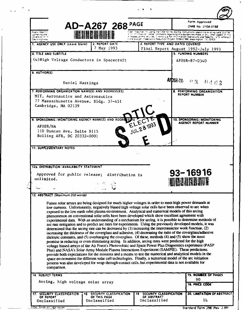
A6Form ApprovedAD-A267 268 PAGE OMB No. 0704-0,88
P. , II - me 1n e''e-nq str c, c q t-nq 3ts c
1. AGENCY USE ONLY (Leave blank) 2 REPORT DATE 3. REPORT TYPE AND DATES COVERED
7 May 1993 Final Report August 1992-July 1993
4. TITLE AND SUBTITLE 5. FUNDING NUMBERS
(u)High Voltage Conductors in Spacecraft AFOSR-87-0340
6. AUTHOR(S)
Daniel Hastings AMSR.TR. • 8 '-
7. PERFORMING ORGANIZATION NAME(S) AND ADDRESS(ES) 8. PERFORMING ORGANIZATION
MIT, Aeronautics and Astronautics REPORT NUMBER
77 Massachusetts Avenue, Bldg. 37-451
9. SPONSORINGiMONITORING AGENCY NAME(S) AND ADOR S) 10. SPONSORING / MONITORINGVO N AGENCY REPORT NUMBER
110 Duncan Ave, Suite B115 P0.'
Bolling AFB, DC 20332-0001
11. SUPPLEMENTARY NOTES
12a. DISTRIBUTION / AVAILABILITY STATEMENT
Approved for public release; distribution is 93-16916unlimited. I I III i
13. ABSTRACT (Maximum 200 words)
Future solar arrays are being designed for much higher voltages in order to meet high power demands atlow currents. Unfortunately, negatively biased high voltage solar cells have been observed to arc whenexposed to the low earth orbit plasma environment. Analytical and numerical models of this arcingphenomenon on conventional solar cells have been developed which show excellent agreement withexperimental data. With an understanding of a mechanism for arcing, it is possible to determine methods ofarc rate mitigation and to predict arc rates for experiments. Using the previously developed models, it wasdetermined that the arcing rate can be decreased by (1) increasing the interconnector work function, (2)increasing the thickness of the coverglass and adhesive, (4) decreasing the ratio of the coverglass/adhesivedieletric constants, and (5) overhanging the coverglass. Of these, methods (4) and (5) show the mostpromise in reducing or even eliminating arcing. In addition, arcing rates were predicted for the highvoltage biased arrays of the Air Force's Photovoltaic and Space Power Plus Diagnostics experiment (PASPPlus) and NASA's Solar Array Module Plasma Interactions Experiment (SAMPLE). These predictionsprovide both expectations for the missions and a means to test the numerical and analytical models in thespace environment for different solar cell technologies. Fimally, a numerical model of the arc initiationprocess was also developed for wrap-through-contact cells, but experimental data is not available forcomparison.
14. SUBJECT TERMS IS. NUMBER OF PAGES
Arcing, high voltage solar array I 9. PRICE COOl
17. SECURITY CLASSIFICATION 18. SECURITY CLASSIFICATION 19. SECURITY CLASSIFICATION 20. LIMITATION OF ABSTRACT
Unclassified Unclassified Unclassitied UL
-- - --- IA C.IAStandard Form 298 (Rev 2-8W

Accesion For....... L NTIS CRA&I
DTIC TABUnannouicedJust i cation
By .. .. ......................B y ................ ................ ...............
Dist, ibution I
Availability Codes
ARCING MITIGAfION AND PREDICTIONS Avail and I or
FOR HIGH VOLTAGE SOLAR ARRAYS Dist Special
by I 1Renee Lynn Mong
Submitted to the Department of Aeronautics and Astronautics
on May 7, 1993 in partial fulfillment of therequirements for the Degree of Master of Science in
Aeronautics and Astronautics
Future solar arrays are being designed for much higher voltages in order to meet highpower demands at low currents. Unfortunately, negatively biased high voltage solar cellshave been observed to arc when exposed to the low earth orbit plasma environment.Analytical and numerical models of this arcing phenomenon on conventional solar cellshave been developed which show excellent agreement with experimental data. With anunderstanding of a mechanism for arcing, it is possible to determine methods of arcrate mitigation and to predict arc rates for experiments. Using the previously developedmodels, it was determined that the arcing rate can be decreased by (1) increasing theinterconnector work function, (2) increasing the thickness of the coverglass and coveradhesive, (3) decreasing the secondary electron yield of the coverglass and adhesive, (4)decreasing the ratio of the coverglass/adhesive dielectric constants, and (5) overhangingthe coverglass. Of these, methods (4) and (5) show the most promise in reducing oreven eliminating arcing. In addition, arcing rates were predicted for the high voltagebiased arrays of the Air Force's Photovoltaic and Space Power Plus Diagnostics exper-iment (PASP Plus) and NASA's Solar Array Module Plasma Interactions Experiment(SAMPLE). These predictions provide both expectations for the missions and a means totest the numerical and analytical models in the space environment for different solar celltechnologies. Finally, a numerical model of the arc initiation process was also developedfor wrap-through-contact cells, but experimental data is not available for comparisons.
2
Contents
Acknowledgements 3
1 Introduction 12
1.1 Background .......................................... 13
1.2 Overview of This Research ................................ 19
2 Numerical and Analytical Models 21
2.1 Conventional Solar Cells ................................ .. 21
2.1.1 Numerical Model .................................. 21
2.1.2 Analytical Model .................................. 27
2.2 Wrap-Through-Contact Cells ............................... 33
3 Arc Mitigation Methods 42
3.1 Control Case ......................................... 42
3.2 Interconnector Material ................................... 45
3.3 Dielectric Thickness ..................................... 47
3.4 Secondary Electron Yield ................................. 48
3.5 Dielectric Constants ..................................... 5o
3.6 Overhanging the Coverglass ............................. 54
3.6.1 Numerical Results ................................. 54
3.6.2 Analysis ....................................... 583.7 Arc Rate Results ....................................... 61
4 PASP Plus and SAMPLE Predictions 66
4.1 PASP Plus ........................................... 66
4.1.1 Experiment Description .............................. 67
4.1.2 Predictions ...................................... 69
4.2 SAMPIE ............................................ 79
4.2.1 Experiment Descripiu~n ............................. 79
4
' I
4.2.2 Predictions ....................................
5 Conclusions 85
5.1 Summary of Results ....................................
5.2 Recommendations for Future Work .......................... S
m m • •5

List of Figures
1.1 Schematic of a conventional solar cell ......................... 13
1.2 Model of the conventional solar array used for numerical simulations .. 6
1.3 Arcing seqence of a high voltage solar array ..................... 18
2.1 Model system of the high voltage solar array and plasma interactions 22
2.2 Grid structure for conventional cell calculations ..... .............. 23
2.3 Typical electric potential contour plot for ambient ion charging of con-
ventional cells ........ ............................... .. 25
2.4 Typical surface charge density along side dielectrics after ambient ion
charging of conventional cells ...... ........................ 25
2.5 Electric field lines over a whisker on conductor surface ............. 26
2.6 Geometry for EFEE charging ............................... 28
2.7 Typical electric field run-away versus time ..................... 29
2.8 Experimental data for ground and flight experiments ............... 32
2.9 Schematic of a wrap-through-contact solar array .................. 33
2.10 Wrap-through-contact solar array model used for numerical simulations 34
2.11 Typical grid structure for calculations .......................... 35
2.12 Typical electric potential for ambient ion charging of WTC cells ..... . 36
2.13 Typical surface charge density along the side dielectric surface after am-
bient ion charging of WTC cells ............................ 37
2.14 Class 1 electric field at upper triple junction versus time .......... .. 38
2.15 Class 2 electric field at upper triple junction versus time .......... .. 39
2.16 Class I surface charge density over the coverglass (a) side surface, (b)
front surface ....... .................................. 40
2.17 Class 2 surface charge density over the coverglass side surface ...... .. 41
3.1 Enhanced field electron emission charging time, ref,, versus W~V for the
silicon conventional control case ........................... 44
3.2 Analytic arc rates for the silicon conventional control case ........... 44
6

t
3.3 Enhanced field electron emission charging time, 7,f,, versus 3V for
different work functions, o,, (eV) ...... ...................... 46
3.4 Analytic predictions and numerical results for Tefee/Tefee(Qtv 4.76eV)
versus 3V .......... ................................... 46
3.5 Enhanced field electron emission charging time, 7,f,, versus 3V for
different dielectric thick'- sses, d(pm) ....................... 47
3.6 Analytic predictions and numerical results for "refe/1i7,e(d = 19opnm.) ver-
sus V ........................................... 483.7 Enhanced field electron emission charging time, rft,, versus 3V for
different secondary electron yields, -f ......... ................... 49
3.8 Surface charge density as a function of distance from the triple junction
for different secondary electron yields, Y.e.. ................ 503.9 Enhanced field electron emission charging time, rf,,,, versus 3V for
different dielectric constant ratios ........................... 513.10 Dielectric side surface charge density before EFEE charging for different
dielectric constants ...................................... 523.11 Electron trajectories for Ed,/1 fd, = 2.7 ......................... .... 53
3.12 Electron trajectories for the control case of Eýd/Ed 2 = 1.3 ............. 53
3.13 Electron trajectories for Ed, /ld, = 0.74 .......................... 54
3.14 Average secondary electron yield over the adhesive versus time for dif-
ferent dielectric constants ................................. 553.15 Model of coverglass overhang ............................. .. 553.16 Enhanced field electron emission charging time, Tefee, versus /3V for
different overhang lengths ................................. 563.17 Class comparison of -rT ef versus ETj for OIV = 3.5 x 10⁵ V ........... 57
3.18 Electron trajectories for 10ILm overhang; ,3V = 3 x 10V ............. 573.19 Electron trajectories for 50pm overhang; 13V 3 x 10'V .............. 58
3.20 Class I dielectric surface potential; O3V = 3x lOV, d, = 10m ...... ... 59
3.21 Class 2 dielectric surface potential; L3V = 3.25x l10V, d, = 5011m . . .. 59
3.22 Analytic arc rates for varying interconnector work functions, 0 ,..... .. 62
3.23 Analytic arc rates for varying dielectric thicknesses, d ........... .. 623.24 Predicted arc rates for varying secondary electron yields, '-Y ............ 63
3.25 Predicted arc rates for varying dielectric constant ratios, Ed,/Ed, . . . .. . . . . 643.26 Predicted arc rates for varying coverglass overhang lengths, d, (pm) . . . 65
4.1 Deployed APEX spacecraft with PASP Plus experiment payload ..... .. 68
7

4.2 Selected arc rate predictions with standard deviation errors for Si conven-
tional array #1 ........................................ 73
4.3 Complete arc rate predictions in the differentiating voltage range for Si
array #1 ........................................... 7:
4.4 Selected arc rate predictions with standard deviation errors for Si conven-
tional array #2 ........ ................................ 74
4.5 Complete arc rate predictions in the differentiating voltage range for Si
array #2 ............................................. 74
4.6 Selected arc rate predictions with standard deviation errors for GaAs/Ge
conventional array #4 .................................. 75
4.7 Complete arc rate predictions in the differentiating voltage range for
GaAs/Ge array #4 ................................... 75
4.8 Selected arc rate predictions with standard deviation errors for GaAs/Ge
conventional array #6 .................................... 76
4.9 Complete arc rate predictions in the differentiating voltage range for
GaAs/Ge array #6 ...................................... 76
4.10 Selected arc rate predictions with standard deviation errors for GaAs/Ge
conventional array # 11 ...... ............................ 77
4.11 Complete arc rate predictions in the differentiating voltage range for
GaAs/Ge array #11 ....... .............................. 77
4.12 Selected arc rate predictions with standard deviation errors for APSA (#36) 78
4.13 Complete arc rate predictions in the differentiating voltage range for
APSA (#36) ........ .................................. 78
4.14 Arc rate prediction comparison for all PASP Plus conventional arrays at
350km ........ ..................................... 80
4.15 SAMPIE experiment package .............................. 81
4.16 SAMPLE experiment plate layout ............................ 82
4.17 SAMPLE arc rate predictions with standard deviation error bars for the
silicon conventional array and APSA .......................... 84
8

List of Tables
3.1 Conventional silicon cell data used in numerical simulations .......... 43
4.1 PASP Plus data used for arc rate predictions ..................... 70
9

S
List of Symbols
A Fowler Nordheim coefficient (1.54 x 10-6 x 104.520•w/•OW A/V 2 )
B Fowler Nordheim coefficient (6.53 x 1091 V/m)
Cdt,,, capacitance of dielectric (F/m 2)Cfrnt capacitance of coverglass front surface (F)
d thickness of dielectric (m)
di thickness of coverglass (m)
d2 thickness of adhesive (m)d,,ap bap distance between cathode and anode (m)
d, distance of electron first impact point from triple junction (m)
do overhang distance of coverglass (m)
do critical overhang distance of coverglass (m)
E, electric field at emission site (V/m)
E, electron incident energy on dielectric plate (eV)E,a,, electron incident energy for maximum secondary electron yield (eV)
ETj electric field at triple junction (V/m)E, electric field of coverglass (V/m)
E2 electric field of adhesive (V/m)
electron current density from conductor (A/M 2)
jee secondary electron current density from dielectric (A/m 2)
JFN Fowler-Nordheim current density from the conductor (A/m 2)jid ion ram current density to the dielectric (A/m 2)
n, plasma number density (M-3 )n., emission site number density (M- 2)m, electron mass (kg)
mi ion mass (kg)
R arc rate (sec-')
r, sheath radius (m)
SFN emission site area determined from F-N plot (M2)
10
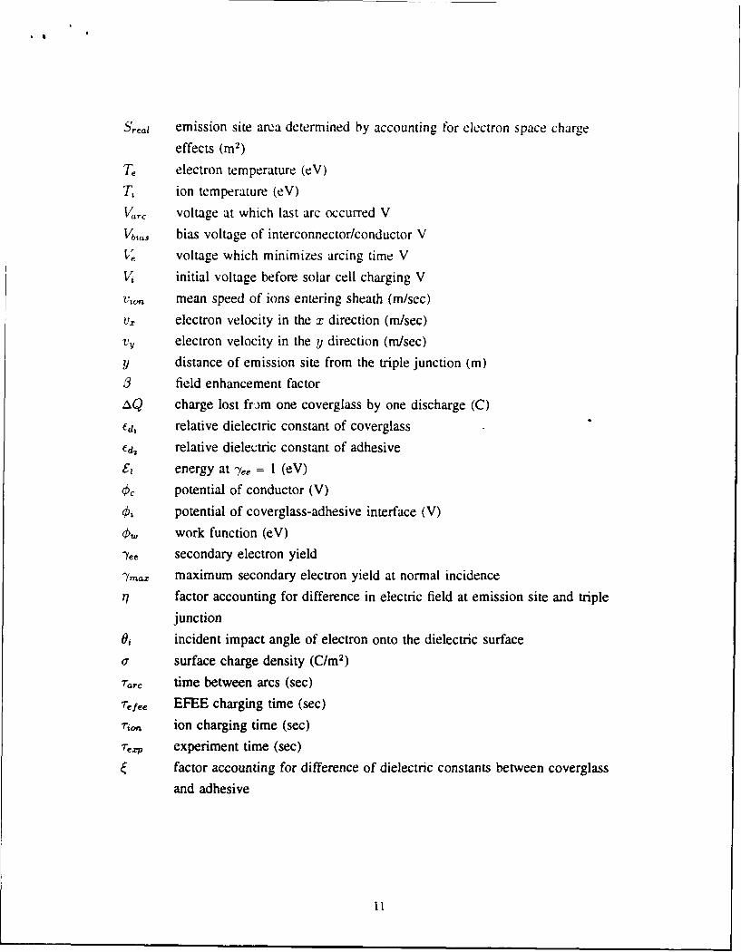
S.eal emission site area determined by accounting for electron space charge
effects (M 2 )
Te electron temperature (eV)
T", ion temperature (eV)Varc voltage at which last arc occurred V
Vbia, bias voltage of interconnector/conductor VVII voltage which minimizes arcing time V
V, initial voltage before solar cell charging V
Vio mean speed of ions entering sheath (m/sec)
vX electron velocity in the x direction (m/sec)VY electron velocity in the y direction (m/sec)
y distance of emission site from the triple junction (m)3 field enhancement factorAQ charge lost from one coverglass by one discharge (C)
Ed, relative dielectric constant of coverglassEd2 relative dielectric constant of adhesive
E,• energy at -Yee = I (eV)
Oc potential of conductor (V)O, potential of coverglass-adhesive interface (V)0. work function (eV)
Yee secondary electron yield
/maxz maximum secondary electron yield at normal incidence77 factor accounting for difference in electric field at emission site and triple
junctionO, incident impact angle of electron onto the dielectric surface
a surface charge density (C/m 2)
Trac time between arcs (sec)
Tefee EFEE charging time (sec)
"rio,, ion charging time (sec)-•e, experiment time (sec)
factor accounting for difference of dielectric constants between coverglassand adhesive
11

Chapter 1
Introduction
In the nast and present, solar arrays used in space have been operating at low voltage
levels, typically biased at '18V. Future solar arrays, however, are being designed for much
higher voltages in order to meet high power demands of the order of 10kW to IMW. High
current levels could be used instead to achieve these increased power demands, but thepower distribution cables would need to be more massive and the resistive losses would
be greater. Consequently, the current is maintained at a low value while the voltage isincreased to attain the necessary power level.
A schematic of a conventional solar cell is shown in Fig. 1.1. The coverglass and sub-
strate shield the solar cell from the environment, mainly to reduce radiation degradation.These are attached to the cell with adhesives. The solar cell itself is a scmiconductor of
two nirts, a p-type semiconductor which has an abundance of electrons and an n-typesemiconductor which has an abundance of electron holes. This construction allows the
solar cell to use the photoelectric effect to convert solar energy into electric power. Aphoton with energy equal to or greater than the energy gap of the solar cell it enters will
free an electron. This creates an electron-hole pair. If the pair is in the p-type semicon-
ductor, the electron will be accelerated across the p-n barrier to the n-type semiconductorwhere it will recombine. The hole, however, will be repelled by the barrier because of
the excess of holes in the n-type semiconductor. Likewise, if the electron-hole pair is
in the n-type semiconductor, the hole will be accelerated across the p-n barrier and the
electron repelled. Consequently, metal interconnectors connect the n-type semiconductorof one cell to the p-type semiconductor of the adjacent cell to utilize the current created
by the electron and hole movement. Solar cells are connected in parallel with metalinterconnectors to obtain desired current levels and connected in series to obtain desired
voltage levels.
The solar array, along with other surfaces of the spacecraft which can allow the passage
of current, collects current from the ambient plasma. In steady state, the spacecraft is
12

SCoverglass
Solar CellPAdhesive
Interconnector
11 ISubstrate
Figure 1.1: Schematic of a conventional solar cell
grounded with respect to the plasma by the zero net charging condition
Op - o (1.1)7-+ Vj -7 0,
which is derived from Ampere's Law and Gauss's Law. To obey this condition, most of
the solar array floats negatively with respect to the plasma This is because tho random
thermal flux of the lighter electrons to the spacecraft is greater than the random flux of
the heavier ions. Therefore, the spacecraft surfaces must be negatively biased in order to
maintain zero net current collection.
High voltage solar arrays, however, have been observed to interact with the plasma
environment of low earth orbit in two undesirable manners. For positive voltages, the
current collection can be anomalously large, possibly leading to surface damage [25].
This phenomenon, known as "snap-over", occurs when the dielectric surface potential
becomes positive, attracting electrons. Above a certain potential, more than one secondary
electron is released by the incident electrons. These excessive secondary electrons are
collected by the interconnector and seen as a current increase, which then incurs a power
loss. For large negative voltage biases, arc discharges can occur [ii]. Arcing observed
in experiments has been defined as a sharp current pulse much larger than the ambient
current collection which lasts up to a few microseconds. This current pulse is usually
accompanied by a light flash at the edge of the solar cell coverglass. Arc discharges can
cause electromagnetic interference and solar cell damage [26], so there is a need to study
mitigation methods and to be able to predict arcing rates with models.
1.1 Background
Arcing has been studied in many experiments and theoretical arguments. The Plasma
Interactions Experiments have been the only space experiments so far, though several
13

space experiments are planned for the near future. Arcing has also been observed in
many grourni tests conducted in vacuum plasma chambers. Two different theoretical
explanations were given by Parks et al. [21] and Hastings et al. [10]. Cho and Hastings
[3] used ideas from both to present a more complete theory of the arcing sequence of
events.
Arcing on solar cells was originally observed by Heron et al. [111 in 1971 during a
high voltage solar array test in a plasma chamber. The array was biased to -16kV, and
arcing was observed as low as -6kV in a plasma density of 10m- 3 .
In 1978, the first Plasma Interactive Experiment (PIX) [61 confirmed that arcing occurs
in space. As an auxilliary payload on Landsat 3's Delta launch vehicle, PIX operated
for 4 hours in a polar orbit around 920km. A solar array of twenty-four 2cmx2cm
conventional silicon cells was externally biased to -1000V. Arcing discharges began at
-750V.
In 1983, PIX 11 [7] was launched also as an auxilliary payload aboard a Delta launch
vehicle into a near circular polar orbit of approximately 900km in altitude. 'he five
hundred 2cmx2cm silicon conventional cells, biased to -1000V, experienced arcing as
low as -255V and at densities as low as 103cm- 3 . The results also found arcing to be
the most detrimental effect of negative biasing.
Ferguson [4] studied the PIX H1 ground and flight results. The interconnectors collected
current proportional to the applied voltage bias. The arc rate R was determined to scale
as
R ;:zen, 1/2 ) ~s (1.2)
where a = 5 for the ground experiments and a - 3 for the flight experiments, n, is the
ambient plasma number density, T, is the ambient ion temperature, and m, is the ambient
plasma ion mass. The dependence of the arc rate on these parameters indicates that the
coverglass surface is recharged by the thermal flux of ions.
Ground experiments revealed more characteristics of the arcing phenomenon. Exper-
iments by Fujii et al. [51 showed that dielectric material near the biased conductor in
the plasma environment is essential for arcing to occur. Fujii et al. tested material plates
biased to high negative voltages in a plasma environment. The plate partially covered
by a 200pim thick coverglass experienced arcing at -450V while the uncovered plate did
not arc, except at -1000V when the arc occurred at the substrate. Snyder [22] measured
the electric potential on the coverglass and found that it decreased significantly when an
arc occurred. This indicates that the negative charge created during arcing discharged the
positive surface charge accumulated on the coverglass surface. Both Snyder and Tyree
14

[23] and lnouye and Chaky [15] observed electron emission from the solar array that
could not be explained by the ambient plasma. Finally, electromagnetic waves generated
from the arcing current were measured by Leung [19].
The first theoretical model was proposed by Jongeward et al. [16] and later expanded
by Parks et al. [211. Jongeward et al. attributed Snyder's [22] experimental observation
of the decrease in coverglass potential prior to arcing to enhanced electron emission from
the interconnector, which corresponds to the electron emission observed in Refs. [23]
and [15]. They suggested the emission is due to a thin layer of ions deposited on
the interconnector, causing the electric field to be significantly increased. The time for
positive charge build up is then dependent on the ambient density n,, the interconnector
size, and the bias voltage. The arc discharge is proposed to occur by a positive feedback
mechanism from electron heating which leads to a space charge limited discharge. At
low ion densities, other surface neutralizing effects are said to dominate, thus inhibiting
the positive charge build up. Jongeward et al. also modeled the arc discharge decay time
by assuming space charge limited conditions and showed that the peak current rifagnitude
agrees well with this assumption.
Parks et al. [211 concentrated on further detailing the theory proposed by Jongeward
et al. [16] on the prebreakdown electron emission current. They accepted Jongeward's
theory of positive charge build-up in a thin insulating layer on the interconnector and
of arcing orginated from interconnector electron emission instead of from the ambient
plasma. Parks et al. proposed the addition of the phenomena presented by Latham
[17, 18], namely that nonmetallic emission processes are significantly responsible for
electron emission by nominally metallic surfaces. Therefore, Parks et al. claimed that the
arc rate must be proportional to the electron emission current density and the bias voltage.
They further suggested that electron emission is controlled by the vacuum electric field
at the surface of the insulator. Given these assumptions, they determined that the rate of
field build-up in the insulator isd
Eo- d(EinsEns - Esns..•ac) = ji + jFN(e P - 1), (1.3)
where f, is the dielectric constant of the insulator layer, E,,. is the electric field inside
the insulator, Ei,-,_ is the electric field at the insulator-vacuum interface, jt is the
ion current density, jFN is the Fowler-Nordheim emission current at the metal-insulator
interface, a is the rate of ionization per unit distance inside the layer, d is the thickness of
the insulator layer, and P is the probability that electrons are emitted from the insulator-
15

.- ,Coverglass Tnple Junction
"%"Adhesive Interconnector
Figure 1.2: Model of the conventional solar array used for numerical simulations
vacuum interface. The emission current from the metal-insulator interface is given by
JFN = AE%2ne-z!--, (1.4)
where A and B are the Fowler-Nordheim emission coefficients, given in Eqns. 1.8 and
1.9. This expression for the electric field accounted for experimental observations of the
characteristics of the voltage threshold, the prebreakdown electron emission current, and
the arcing rate.
Hastings et al. [ 10] did not try to explain the prebreakdown electron emission current
but instead proposed a model for the gas breakdown seen as the arc discharge. They
suggested that neutral gas is desorbed from the sides of the coverglass by electron bom-
bardment, a phenomena known as electron stimulated desorption (ESD). The bombarding
electrons are emitted from the interconnector, as determined from Snyder's experiments
[221, and from the coverglass as secondary electrons which return to the side surface.
The desorbed neutrals then accumulate in the gap between the coverglasses over the inter-
connector, forming a potentially high-pressure gas layer which can break down from the
electron emission current flowing through it. This was in contrast to the previous theory
which suggested that the arc occurs in an insulator on the surface of the interconnector.
Recent work by Cho and Hastings [3] combined some of the ideas from these two
theories and studied the charging of the region near the plasma, dielectric, and conductor
triple junction. The model that they studied is shown in Fig. 1.2. The dielectric consists
of both the coverglass and the adhesive bonding the coverglass to the solar cell. The
conductor is the interconnector, which is usually placed between the cell and substrate
on one end and between the cell and cover adhesive in the adjoining cell. The solar cell
itself was neglected since the potential drop across it is at most a few volts while the
potential drop across the coverglass and adhesive is hundreds or even thousands of volts
for high voltage operation.
Cho and Hastings developed a numerical simulation of the arc initiation processes.
They studied charging of the dielectric surfaces by three sources: ambient ions, ion-
induced secondary electrons, and enhanced field electron emission. From numerical
16

results, they determined the following arc sequence, illustrated in Fig. 1.3:
(1) ambient ions charge the dielectric front surface, but leave the side surface
effectively uncharged;
(2) ambient ions induce secondary electrons from the conductor which charge the side
surface to a steady state unless enhanced field electron emission (EFEE) becomes
significant;
(3) EFEE will charge the side surface if there is an electron emission site close to the
triple junction with a high field enhancement factor, 3; and
(4) EFEE can result in collisional ionization of neutrals desorbed from the coverglass,
which is what is observed as the arc discharge.
They also found that the electric field at the triple junction is not bounded during EFEE
charging.
Cho and Hastings used the numerical results to develop analytical formulas describing
the arcing rate [3, 9]. They suggested that the time between arcs is the minimum of the
sum of the ambient charging time ri, and the enhanced field electron emission charging
time Tefee, so that the arc rate R is given by:
R = min(Tron + 7efee))- (1.5)
For the ion charging, Cho and Hastings showed that ambient ions mainly charge the front
surfaces of the coverglass, not the side surfaces. They expressed this time as
7"ion = - eio~aQ
where AQ is the charge lost by the coverglass due to an arc discharge, which must be
recovered; enevi, is the ambient ion flux to the front surfaces, with vi as the mean
speed of ions entering the sheath surrounding the solar array; and A, 1 is the frontal area
of the coverglass. Assuming a constant secondary electron yield and constant voltage
bias, they derived the following analytical expression for the EFEE charging time, r,,,e:
Tefee (Cdiel di exp d' (1.7)
=-y-1)V a7A s-- BO /eVxp
where A and B are the Fowler-Nordheim coefficients given by
1.54 x 10-6104.52/V'(1.8A = 0.(1.8)
6.53 x 10 Ow , (1.9)
17

electric sheath
(charging•coverglass of front
+- +- surface
*-V interconnector
secondary electronmultiplication charging.
(9 (Dof sidesurface
•=-V enhanced field emission
discharge
o J discharge
+ 0) + ambientr "-",...•1on s
recharging___________by ions
Figure 1.3: Arcing seqence of a high voltage solar array
18
,c is a factor to account for the difference in dielectric constants and is given by
c [2+ d , •(d - d2)l-
co is c evaluated with d, = d, d1, is the distance from the triple junction of the first impact
by an electron emitted from the conductor, CGdee is the capacitance of the dielectric atthis impace site, --,, is the secondary electron yield of the dielectric, Sreai is the real areaof the emission site, SFN is the Fowler-Nordheim "effective" area of the emission site, qj
is a factor to account for the difference in the electric field at the emission site from the
triple junction, di is the thickness of the coverglass, d2 is the thickness of the adhesive,
d = d, + d2, V is the voltage at which the arc occurs, and ,3 is the field enhancement
factor. From comparison with experiments, Hastings et al. [91 suggested that 3 must be
greater than a few hundred, so they assumed that the field enhancement is due to a thindielectric layer on the conductor surface rather than microprotrusions. They later updated
their views as explained in Section 2. 1. 1.From experimental observations, Hastings et al. [9] suggested other characteristics of
the arcing processes, such as the discharge wave hypothesis and the occurrence of onearc at a time within a certain area. The discharge wave hypothesis suggested that at-c initiation emitted electrons form a plasma cloud over the solar array. Some of the
electrons, attracted by the positive surface potential, strike the coverglasses in the localarea until they are discharged. Experimental results also showed that the arc currentis more likely to be carried by electrons, consistent with the hypothesis that arcing isinitiated by electron emission from the interconnector. In addition, as the temperature
increased fewer neutral gas molecules were desorbed from the dielectrics and the arc ratewas seen to decrease, consistent with the hypothesis that ionization of the neutral gases
also plays a role in arc initiation.
1.2 Overview of This Research
Power requirements for space systems are increasing significantly. As the most reliable
power source, high voltage solar arrays will be needed to meet these requirements. Sincearcing degrades the array performance and causes electromagnetic interference which
affects nearby instruments, it is imperative to study arcing. Recent studies by Cho andHastings (3, 9] determined an arcing sequence of events and an arcing rate based on
numerical and theoretical work which has been shown to agree well with experimental
results. With these models it is possible to determine methods of arc rate mitigation and
19

to predict arc rates for experiments. This research can then be used in the design of new
solar cells and in the design of high voltage solar arrays.
The focus of this research is twofold: to identify and study mitigating effects on arc
rates and to present arc rate predictions for two space experiments soon to be launched.
In Chapter 2 the numerical and analytical nodels developed by Cho and Hastings are
reviewed, and the numerical model modified for the wrap-through-contact solar cell ge-
ometry is presented. Based on the analytical model for conventional solar cells, arc rate
reduction methods are studied using the corresponding numerical model in Chapter 3. In
Chapter 4, arcing rates are predicted for the high voltage biased arrays of the Air Force's
Photovoltaic and Space Power Plus Diagnostics experiment (PASP Plus) and NASA's
Solar Array Module Plasma Interactions Experiment (SAMPIE). Finally, conclusions are
summarized and future work is suggested in Chapter 5.
20

Chapter 2
Numerical and Analytical Models
2.1 Conventional Solar Cells
A schematic of a conventional solar cell is shown in Fig. 1.1. In high voltage operation,
the voltage differential over the coverglass and adhesive can be hundreds or even thou-
sands of volts while the voltage differential over the cell itself is at most a few volts.
For modeling purposes, the cell semiconductor can therefore-be neglected, as shown in
Fig. 1.2. In this model, the interconnector is a conductor and the coverglass and adhesive
are dielectrics. The numerical and analytical models used for conventional cells were
developed by Cho and Hastings [3, 9], as briefly described in Section 1.2.
2.1.1 Numerical Model
The numerical model incorporates all relevant physical characteristics and processes for
solar cell charging from the ambient plasma, electron emission from the interconnector,
and secondary electron emission from the dielectrics. A representation of this system is
shown in Fig. 2.1. The coverglass and adhesive surface charge densities are affected by
the ion ram current density jid, the electron emission current density from the conductor
jec, and the secondary electron current density from the surface j,,. After arc initiation,
the current densities from the ionization of neutral gases may also be significant. These
are not considered, however, as only the time to arc initiation is the focus of this research.
The rate of change of the dielectric surface charge density can then be expressed asda-(Xt) = jid(Xt) 0 P(x, y,t)j (y,t)dy - f P(x, x', t)je(x')dx' + j.e(x,t), (2.1)
where P(x, y, t) is the probability that an electron emitted from position y on the conductor
hit the dielectric at position x at time t, and P(x, x', t) is the probability that an electron
emitted at x' hits the dielectric at x.
21

dielectric(coverglass, adhesive)
frontsurface
conductor '4"(interconnector) i id (ion current ambient
"rl to dielectric) plasmajunction • 'nto e J(electron current
from conductor)
Jic (ion current 4- Jrem-V "," ,• to conductor)
V -, 1 ,,.(secondaryside . electron on sheathsurface , d dielectric) edge
L! X
Figure 2.1: Model system of the high voltage solar array and plasma interactions
The numerical model consists of three schemes. The first scheme uses the capacitance
matrix method to obtain a preliminary electric potential distribution along the dielectricsurfaces. The second scheme involves a particle-in-cell (PIC) method which is used forambient ion charging. Once a steady state is obtained from the ion charging, a space-
charge-free orbit integration scheme calculates the electron charging by enhanced field
electron emission (EFEE).All schemes use the same computational domain and grid. The phase space of the
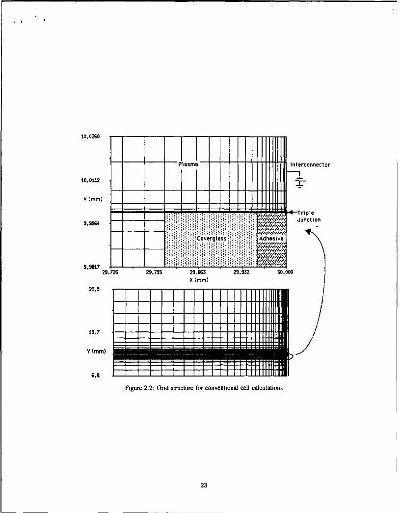
domain consists of two position coordinates and three velocity coordinates. As shown ;nFig. 2.2, the domain includes two halves of solar cells with the interconnector forming
the lower boundary of the gap between the cells. The boundary condition far from the
cells at x = 0 is € = 0, simulating the far field. In these simulations, any electrons leavingthe domain at x 0 will also leave the sheath. The boundaries are thus Dirichlet in the
x direction and periodic in the y direction to simulate a solar array. The grid is clusteredalong the dielectric sides and near the interconnector for better resolution of the large
electric potential gradients in these areas.
The capacitance matrix method is used to obtain an inititial condition for the PICcode, thus reducing the simulation time. In employing this method, which is given in
22
10.0260 -
i:.ozlasm - _ _-i nterconnector
~ Triple
9. 9964.... Jnto
Cverg ass Aduncesio
9.M8729.726 29.J95 2.02.3 00
X (mm)
20.5 - - - - - - - - - -
13.7 - - - - - - - - - - -/
Y (MM)
Figure 2.2: Grid structure for conventional cell calculations
23

Ref. [14], a unit charge is ascribed to one cell on the dielectric surface while all other
cells have zero charge. The Poisson equation is then solved to determine the electric
potential in every cell on the dielectric surface due to this unit charge. This process is
repeated for each grid cell along the surface of the dielectrics. Afterwards, the array
containing all of the potential values calculated is inverted to determine the capacitance
value for each grid cell. This matrix is stored for use as the initial conditions of the PIC
code, so that the simulation can be started from any charging state described by only the
surface charge or the surface potential.With the capacitance matrix calculated for unit charges, the PIC code calculates the
space potential based on a pre-determined surface potential. The initial conditions for
the dielectric potential are 0 = 0 on the front surface and a linear distribution of 0 on
the side surface with the conductor voltage at one end and the front surface zero voltage
at the other end. The ram velocity is oriented 901 to the dielectric front surfaces and
conductor. To save computational time, an artificial ion mass is used such that m,/m, =
100. Ions and electrons are initially inserted uniformly throughout the domain Sccording
to the ambient density. After the space potential is calculated using the Poisson equation,
the ions and electrons are moved according to the new potential. A new space charge
density for each grid point can then be calculated based on the new ion and electron
positions. This loop is then repeated with the potential being re-calculated based on the
new charge density. The PIC code is run for a time equivalent to the inverse of the ion
plasma frequency to adjust the space charge completely with the surface potential.
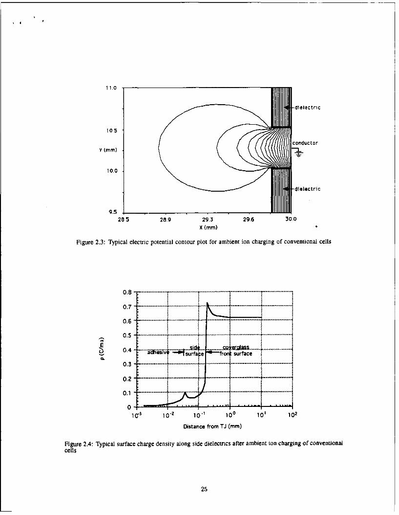
The results from the PIC scheme are the initial conditions for the dielectric charging
scheme. A typical contour plot of the initial electric potential is shown in Fig. 2.3, and
the corresponding surface charge density is shown in Fig. 2.4.
No electron emissions from the conductor or dielectric are taken into account in the
PIC code since they are negligible. The electron emission which leads to arc initiation
was determined to be enhanced field electron emission (EFEE) by Cho and Hastings [3].
They described this current density from a finite emission site on the conductor surface
as
.h(y) = A -'N 02 E2 exp -- , (2.2)
which is the Fowler-Nordheim expression for field emission due to a thin dielectric layer
with the added factor SFNI/SaO to account for the negative space charge effect near the
emission site. The electric field E in this expression is the electric field at the dielectric-
vacuum interface. A and B are the Fowler-Nordheim emission coefficients given by
Eqns. 1.8 and 1.9. The field enhancement factor 0 is assigned to the emission site
24
11.0
10.5
conductor
Y (Mm) --1
10.0
I dieleoctric
9.5
28.5 28.9 29.3 29.6 30.0
X (Mm)
Figure 2.3: Typical electric potential contour plot for ambient ion charging of conventional cells
0.8 -................................
0.7 8 .
0.6
0.5 .0 . .................................... .... ..... ........ ..................... .•g r l ......... ......."......... ..... ...... ..... ..... .....
Z3 0 - aanesiv* "- surfai:e fronk surface
0 .3 .................... ....................... . ......... 4 .......... ........................ .
° " ........................... ... ................... .........................0. ........ ....................... ... ... .. r ........
103 10o-2 10-1 100 10, 102
Distance from TJ (mam)
Figure 2.4: Typical surface charge density along side dielectrics after ambient ion charging of conventionalcells
25

hh
Figure 2.5: Electric field lines over a whisker on conductor surface
to represent an enhancement due to manufacturing defects or impurities. As shown in
Fig. 2.5, the protrusion causes a higher electric field gradient which enhances the electric
field at its tip. From electrostatic theory for a whisker, 3 is the factor of the enhanced
electric field at the tip of the whisker defect relative to the average electric field in thevicinity is equivalent to the ratio of the height of the protrusion to its radius of curvature.
This factor can be of the order of 1 to 101, with typical values of interest in the hundreds.
"The secondary electron current density at each point x is given by
jee(X, t) = f Je(X, y)P(x, y, t)jec(y, t)dy + f y,.(x, x')P(x, x', t)jee(x')dx'. (2.3)
In the orbit integration scheme, the first term in Eqn. 2.1 is neglected since it was shown
to be insignificant during electron charging [3]. Using Eqn. 2.3, the surface charge density
equation can be rewritten as
da(x, t) frdt = ] (Yee (x, y) - 1)P(x, y, t)jec(y, t)dy+f (%y(x, x') -1)P(xX',t)jee(x')dx'. (2.4)
The orbit integration scheme then consists of
(1) obtaining the surface potential by using the capacitance matrix method;
(2) solving Laplace's equation to obtain the space potential;
(3) integrating test electron orbits from the conductor to calculate -y,, and the impact
probabilities P for a given electron current density from the conductor;
(4) solving Eqns. 2.1 and 2.3 for the secondary electron current density j,. and the rate
of change of the surface charge density;
(5) renewing the surface charge density;
(6) obtaining the new potential for the renewed surface charge density;
(7) calculating the timestep;
(8) determining if the space charge current density is too high or the tinestep is too
small, either of which will halt the program; and
26
(9) calculating electron trajectories.
Steps (4) through (9) are repeated until the specified number of timesteps are completed
or the progam is stopped in step (8). If the space, charge current density is too high, thespace charge effects of the emission current can no longer be neglected so the PIC code
must be run if further calculations are needed. If the timestep is too small, the electric
field is most likely running away.
The timestep for EFEE charging is calculated based on the rate of change of thedielectric surface charge density at the first impact point x = d,. This can be expressed
by neglecting the second term in Eqn. 2.1, reducing the equation to
fd d = 1 .1 P(x,.y t)dx( - i)jc(yý t)dy. (2.5)
The integral fd, P(x, y, t)dx is approximately unity since the point x = d, is the first
impact point by emitted electrons. The equation then simplifies todcd
dt ' = ('Ye - O)jec(y.t)v-0VS, (2.6)
orAt = , (2.7)
(%e - 1)jey, t)(1v-/d,)'
where S is the area of the emission site, as shown in Fig. 2.6. The potential difference
between the triple junction (x = 0) and the impact point (x = di) can be expressed as
01Od- Cdzae' (2.8)
where Cd,,Le is the capacitance of the dielectric surface and a is the surface'charge density.
The electric field, then, is approximately
E" (2.9)Cdwiedti
The timestep can therefore be determined by solving
At = 0.02 ECded(2.10)
(-yee - 1)jec(y,t)(V3/do)'
where the empirical factor 0.02 is used so that the timesteps will be shorter than the
actual timescale of arc initiation.
2.1.2 Anaulytical Model
The analytical model, which is used to calculate the arc rates, is drawn from the theory
of Cho and Hastings [3, 91, discussed in Section 1.2. The arc rate is determined by
27
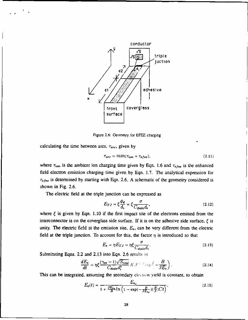
. I
conductor
-Is; tripleuction
d2 7
dl adhesive
front coverglasssurfac e
Figure 2.6: Geometry for EFEE charging
calculating the time between arcs, Tarc, given by
Tarc = min(r",., + refe), (2.11)
where -rim is the ambient ion charging time given by Eqn. 1.6 and Tefe is the enhanced
field electron emission charging time given by Eqn. 1.7. The analytical expression for7efee is determined by starting with Eqn. 2.6. A schematic of the geometry considered is
shown in Fig. 2.6.The electric field at the triple junction can be expressed as
ET = cd = - 0 (2.12)
di CdieLed'
where C is given by Eqn. 1.10 if the first impact site of the electrons emitted from the
interconnector is on the coverglass side surface. If it is on the adhesive side surface, ý is
unity. The electric field at the emission site, E•, can be very different from the electric
field at the triple junction. To account for this, the factor 17 is introduced so that
E, = T/ETJ i=C ~ 1 (7 (2.13)
Substituting Eqns. 2.2 and 2.13 into Eqn. 2.6 results in
dE -(Ye1)V3~g p B)2 E ( (2.14)
This can be integrated, assuming the secondary eVlcuton yield is constant, to obtain
E, (t) = Eo (2.15)1 + n In(- exp(-r-)( ct)2
28
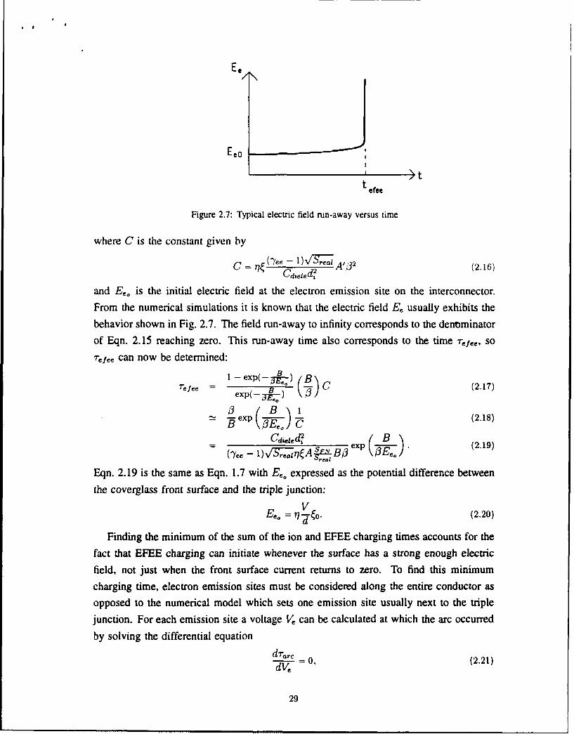
E.i
Eeo
t efee
Figure 2.7: Typical electric field run-away versus time
where C is the constant given by
c " -_1'A132 (2.16)Cdieled
and Eo is the initial electric field at the electron emission site on the interconnector.
From the numerical simulations it is known that the electric field E, usually exhibits the
behavior shown in Fig. 2.7. The field run-away to infinity corresponds to the denOminatorof Eqn. 2.15 reaching zero. This run-away time also corresponds to the time Te,!,, so
Tref can now be determined:
"refee = e - C (2.17)exp( B ) 0
exp (2.18)
=d,, d', i2 )• A,',B- exp ( B (2.19)
Eqn. 2.19 is the same as Eqn. 1.7 with E,. expressed as the potential difference between
the coverglass front surface and the triple junction:
VEe. = 7-•-o. (2.20)
Finding the minimum of the sum of the ion and EFEE charging times accounts for the
fact that EFEE charging can initiate whenever the surface has a strong enough electric
field, not just when the front surface current returns to zero. To find this minimum
charging time, electron emission sites must be considered along the entire conductor as
opposed to the numerical model which sets one emission site usually next to the triple
junction. For each emission site a voltage Ve can be calculated at which the arc occurred
by solving the differential equation
d = o, (2.21)
29
or
d ( e (V-,-•, +'n (C )• f, Aile 2 X •Fd Ye- Vrc- -)C~ -1 + Gdce~exp (Bd 0
7141en;'~ cell (-te - 1)vT'_az1cA!FvB3 31c I 0
(2.22)
where Varc is the voltage of the last arc discharge and Cfr, is the capacitance of the
coverglass front surface.
In order to solve Eqn. 2.22, a number of properties must be known or determined.First, the following cell properties must be known: the thickr.. ss of the coverglass and
cover adhesive (dl,d 2), the dielectric constants of the coverglass and adhesive (Edt,,d 2 ),
the energy of incident electrons for maximum secondary electron yield for the coverglass
and adhesive (Emx, ,Ema_,,), the maximum secondary electron yield at normal incidencefor the adhesive and coverglass (y,-y,3, ), the interconnector work function (0w,),
and the solar cell frontal area (Ac,,). Then, the following factors can be determined: Aaccording to Eqn. 1.8; B from Eqn. 1.9; ý and o from Eqn. 1.10; d = di + d2; Cfr o,which is approximated as
= (Aceuld,)/dl + (AclLd,)/d 2 (2.23)
and -y,, which is given by [8]
-Yee = e•n mj exp 2-2 - I exp[2(1 - cos O,)l. (2.24)
Here E, is the incident energy of the emitted electrons impacting the dielectrics given by
E,= ETJdI = LoVdt (2.25)Sd
and O, is the incident angle of those electrons at the first impact site given by
0i = arctan ( ,) , (2.26)
where y is the distance of the emission site from the triple junction. The mission param-
eters determine the ion velocity v,1 and the range of the ambient density ne. If the array
is orientated at 900 to the ram velocity, vi is the orbital velocity. Otherwise, vi.. is asum of the orbital velocity and the mean thermal speed of ions 6,/4, where
8r = Ti (2.27)7 rm,
Consequently, the ion mass and electron temperature must also be known. For eacharc calculation, n, is chosen randomly from a uniform distribution in Ioglo n,. Other
30
properties only known within a range include areas Sq f and Sr,,L and enhancement factor
3. Areas Seif and Sre,a are randomly chosen from uniform distributions in log 10 Sf f and
logio Sreoa, respectively, between given minimum and maximum values. The enhancement
factor 3 is randomly selected from the distribution f(3) = foexp(-3/1 3), where f" is
determined from the normalization: f f(3)d0 = 1. Finally, the three parameters left to
be determined are Cdiete, di, and rq, all of which are functions only of the emission site
distance y from the triple junction. To determine C'diie, the capacitance matrix scheme
used with unit surface charge values must be run. The relevant values are the diagonal
elements. Those that correspond to the lower side dielectric are non-dimensionalized by
the normal capacitance 1ý- + d (2.28)
and inverted. The corresponding distances from the triple junction are non-dimensionalized
by the thickness of the two dielectrics, d. These values are plotted and fit to a five orderpolynomial:
ile 1: Cn (2.29)
To determine d, and 17, results from the orbit integration scheme of the numerical model
are used to obtain functional forms. These are
= bn d(2.30)
and771 ' E an((9 -- 1 -1) (2.31)
fl= I
where ) = Y/(dgap/2).
The voltage V, is determined to be in the range of V,, the voltage differential between
the front surface and conductor just after the arc, and Vba1 . If 7f,, dominates to the point
where ri.. is insignificant, V, = Vi. Likewise, if -,on dominates, Ve = Vb1,. Otherwise,
the arcing time is affected by both T-rfe and -,m, so V,, is determined by the Newton-
Raphson method. After rar is calculated for every emission site, typically numbering
1000, the smallest Tar, is compared with the experiment time, Tez. If r'e,, is greater than
-arc, another rc is calculated until the sum of the arcing times is greater than -r',-p. The
arc rate is then the number of arcs counted less one divided by the experiment time.For a given solar array, the surface is divided into sections of area equivalent to
the area covered by the arc discharge wave. Based on experimental measurements in
Ref. [9], this area is chosen to be 0.012m2 . All arcs in a section are assumed to be
31

100
10*1
0-. O" . o
10'2r~-' 0
- PIX .1 flight
2 10.3 Threshold ,l"S / ,-• ,1 ,a PIX 11 ground
S/r'0 Leung
10 4 X Miller
/ - kNumerical flight
Nu.......Nmerical ground
10-5 __ _ __ _ __ _ __ _ __ _
200 300 500 1000
Negative Bias (Volts)
Figure 2.8: Experimental data for ground and flight experiments
correlated, but arcs are assumed to be uncorrelated between different sections. The arc
rate is calculated for each correlated area independent of the other areas. If there is more
than one correlated area, the actual arc rate for the array is the sum of the arc rates of
each area.
Cho and Hastings use this procedure in Ref. [3] to calculate the arc rate numerically
for the PIX II flight and ground experiments. As can be seen in Fig. 2.8, the results
show excellent agreement with the data over the range that the data exists. They predict
a threshold when the charging process is exponentially slow and also predict a saturation
for high voltages. The lower parts of the curves cover the regime where the enhanced
field electron emission charging is the slowest charging process in the system. The arcrate dependence on voltage here is exponential and enables a threshold voltage to be
defined with a small uncertainty. This threshold voltage can be defined as the voltage at
which the arc rate is decaying very rapidly. The upper parts of the arc rate curves cover
the regime dominated by the ion recharging time. This leads to a decrease in the rate
of change of arc frequency as can be clearly seen in the data. The fact that the arc rate
scales with the density for the higher voltages can also be explained from the dominance
of the ion recharging time since this scales directly with density.
32
Coverglass/j- Silicon Cell /Wrap-through hole
.. o..=............ ....... ................. •......... ..... .............. ° °. . ° ......... °..... o.......... ............. •............
,. o. . . . . . . . . . . . . °. . . . . .. . . . °. . . . . . . . . =... . . . . . . ... M° . . . . . = . . . .
apton Substrate Metal Interconnector
Figure 2.9: Schematic of a wrap-through-contact solar array
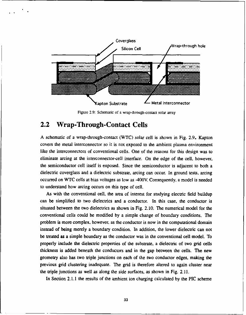
2.2 Wrap-Through-Contact Cells
A schematic of a wrap-through-contact (WTC) solar cell is shown in Fig. 2.9. Kapton
covers the metal interconnector so it is not exposed to the ambient plasma environmentlike the interconnectors of conventional cells. One of the reasons for this design was to
eliminate arcing at the interconnector-cell interface. On the edge of the cell, however,
the semiconductor cell itself is exposed. Since the semiconductor is adjacent to both adielectric coverglass and a dielectric substrate, arcing can occur. In ground tests, arcingoccurred on WTC cells at bias voltages as low as -400V. Consequently, a model is needed
to understand how arcing occurs on this type of cell.
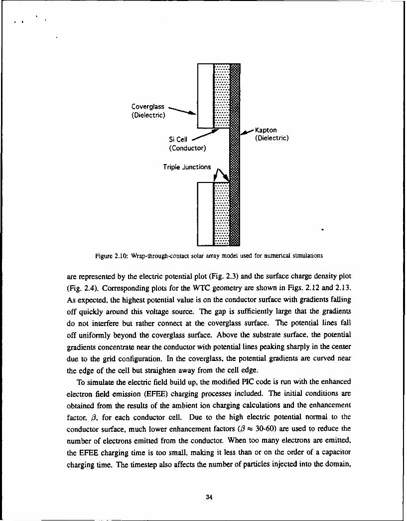
As with the conventional cell, the area of interest for studying electric field buildupcan be simplified to two dielectrics and a conductor. In this case, the conductor is
situated between the two dielectrics as shown in Fig. 2.10. The numerical model for theconventional cells could be modified by a simple change of boundary conditions. Theproblem is more complex, however, as the conductor is now in the computational domaininstead of being merely a boundary condition. In addition, the lower dielectric can not
be treated as a simple boundary as the conductor was in the conventional cell model. Toproperly include the dielectric properties of the substrate, a dielectric of two grid cellsthickness is added beneath the conductors and in the gap between the cells. The new
geometry also has two triple junctions on each of the two conductor edges, making the
previous grid clustering inadequate. The grid is therefore altered to again cluster nearthe triple junctions as well as along the side surfaces, as shown in Fig. 2.11.
In Section 2.1.1 the results of the ambient ion charging calculated by the PIC scheme
33
S S
Coverglass(Dielectric)
Si Cell /(Dielectric)
(Conductor)
Triple Junctions
Figure 2.10: Wrap-through-contact solar array model used for numerical simulations
are represented by the electric potential plot (Fig. 2.3) and the surface charge density plot
(Fig. 2.4). Corresponding plots for the WTC geometry are shown in Figs. 2.12 and 2.13.
As expected, the highest potential value is on the conductor surface with gradients falling
off quickly around this voltage source. The gap is sufficiently large that the gradients
do not interfere but rather connect at the coverglass surface. The potential lines fall
off uniformly beyond the coverglass surface. Above the substrate surface, the potential
gradients concentrate near the conductor with potential lines peaking sharply in the center
due to the grid configuration. In the coverglass, the potential gradients are curved near
the edge of the cell but straighten away from the cell edge.
To simulate the electric field build up, the modified PIC code is run with the enhanced
electron field emission (EFEE) charging processes included. The initial conditions are
obtained from the results of the ambient ion charging calculations and the enhancement
factor, 03, for each conductor cell. Due to the high electric potential normal to the
conductor surface, much lower enhancement factors (W3 s 30-60) are used to reduce the
number of electrons emitted from the conductor. When too many electrons are emitted,
the EFEE charging time is too small, making it less than or on the order of a capacitor
charging time. The timestep also affects the number of particles injected into the domain,
34

,Ill .! ! l llDieloectricDielectric-ý :Con ductor:
Triple Junctions
21.0
14.0 - -
7.0
0.0 0.0 7.5 15.0 22.5 30.0
Figure 2.11: Typical grid structure for calculations
35

di electric /conductor
10.72
Y (mm) dielectric
10.30
9.8828.47 28.85 29.23 29.62 30.00
X (mm) dielectric conductor
Figure 2.12: Typical electric potential for ambient ion charging of W'I'C cells
so it is typically chosen to be w•At = 0.01. Larger timesteps can be used when fewerparticles are in the domain, which occurs when the electric field at the triple junction hasnot increased enough for EFEE charging to begin. The PIC code is run until the electricfield runs away at one or both of the triple junctions. Since the PIC code automaticallyaccounts for space charge effects, the simulation is often run beyond the electric fieldrunaway into the space charge current limited regime, which limits the electric fieldmagnitude.
The cell properties used for the WTC simulations are based on the Space StationFreedom WTC cell. The coverglass and semiconductor are each 203,um (8 mil) thick, andthe cell gap is 1mm. The semiconductor is silicon, which has a work function of 4.85eV.The coverglass is assumed to be ceria-doped microsheet (CMX) with a dielectric constantof 4 and secondary electron properties of E,, = 400V and y,,. = 4. The Kaptonsubstrate has a dielectric constant of 3.5 and assumed secondary electron properties ofE,,. = 300V and -y,,. = 3.
The EFEE charging of the WTC cells over the range of 300-500V is distinguishedby two classes of behavior, the first occurring with lower 03 (,30) values and the secondoccurring with higher 03 (-50-60) values. As seen in Figs. 2.14 and 2.15, the electric
36

0 .4 ...... . . .............. . ..... ........ . .... .. ..... ... ...... ........ . .............. . ........ .... . . .............. . ..........0 .2 ......... .............. . ..... ........ . ii .... .... ......... ....... ... .... .....
0~~~~~ ~ ~ .................. ................ ... .... .. ............... . .
02--0.2
S-0 .2 . ....... ............... . ..... .. ...... ........ . ....... ...... . .............. . ........ s.... . .............. . ..........
-0 .4 - -- ... . ....... . .... ....... . ... • .... ............ ....... . .............. ..... ......... "
-0.6 '..... .i.-0.8~~ ---- -.-....-........... . .... ' . ... '
-0, Substrete,0.01 0.1 1 1 0 100
Distance from upper triple junction (ram)Upper TJx Lower
TIJ
2 0 -.. ..- ..---.--. ... .... .. ..... .. ..... ......... ........ ... ...... .. .i0 ... .. .... .......... . . .... .
•" -200 - . ....... .............. . ....... •.. . .. ........... ....... ....... --- ---------
EU
S -6 0 0 - -- ... .......... ....... .................. ......... .... .......... . .................. .. ...........-800 2 ... .. ... ... ..... ......... ........ ........
- 10 0 0 ... ... ......... ....... ....... .. .............. . ....... ...... . .............. . .............. . ...----........... ...........-1200.
10.4 1013 10.2 10"t 100
Distance from lower triple junction (mm)
Figure 2.13: Typical surface charge density along the side dielectric surface after ambient ion charging ofWTC cells
37

2 I
3 .0 1 0 . ......... .............. . . . ........... ...................................... ... ................ " ... .......... .
S2 .84 1 0 5 . ............. ............. .. ............... .. . . .. . . . .............. . ........ ......... .....2.6 10~ ........
S :2 .2 .1 0 .............. ............... ............... .............. .................. .................. .............. S2.4 10C.
2.210.
2.0 10.
1.6 10 ............. .. ................ ........... ........ ......
1.4 10s -
0.0 100 4,0 10" 8.0 10"s 1.2 10.4
time (sec)
Figure 2.14: Class I electric field at upper triple junction versus time
field at the upper triple junction increases initially for the first class and decreases initially
for the second class. No runaway occurs at the lower triple junction within this time.
In the first class, the ambient ion charging continues to build up the electric field at the
upper triple junction until it is high enough to initiate EFEE charging. Once initiated, the
high flux of electrons causes the field to decrease for a short time before the runaway. As
shown in Fig. 2.16, the surface charge along the side of the coverglass does not change
much during the ambient ion charging, as expected, but also does not change much
during the electric field runaway. The surface charge along the front surface, however,
does increase substantially, indicating that the electrons from the conductor are striking
there and increasing the surface charge through secondary electron emission.
In the second class of behavior EFEE charging begins immediately, emitting many
electrons into the domain. Although the surface charge density does increase, as shown
in Fig. 2.17, most of the electrons quickly exit the domain without striking any of the cell
surfaces. Just prior to runaway, the difference between the number of electrons emitted
and the number of electrons impacting the dielectric increases substantially at the same
time that the total number of electrons in the domain increases substantially. The electric
field then runs away, and the surface charge density along the coverglass side and front
surfaces increases significantly.
38

4.5 10~ ....................................... ..... ..... ...... .. .
E 4.0 10~ 6 ..........:............ ... .... ....
> S
3 .5 1 0 s . ............................. ................ ....................................... ..... ........................ .
3 .0 1 0 ' ... ..................................... ........................ .............. ....... i ........................
2 .0 1 0 s . ............................................ ..................... ............. ...... ... ................... . . .
3 .0 .0 ........ ............. ............................................... .......... .. ........ ......................:1.5 10 -
I-
w, 1 .0 1 0 S .......... .................................................... .......... .......... .......................
a.
60 1
0.0 10OP 5.010- 1.0 10"7 1.5 10 7 2.0 10- 2.5 10,7
time (sec)
Figure 2.15: Class 2 electric field at upper triple junction versus time
39

0 ...... ........ ... ......... ....... ......... . ...
-After ambient ion-0 5 .......... j..... .. ............. - r--IV PiaI EKiE charging
MU Before runaway
-0.80.04 '6 0.08 0.1 0.12 0.14 0.16
Distance from upper Ti (mm)
(a) Covergiass side surface
100. .......... .. - Ambient ion charging
-0- Initial EFEE charging
10- ......... .........-.... Before runaway- -During runaway J
0.1 ...... ............ ......... ........ ..................
0.01 ....... .. ... . ........... . .................... 4... .....
0 2 4 6 8 10 12Distance from upper Ti (mm)
(b) Covergiass front surface
Figure 2.16: Class 1 surface charge density over the coverglass (a) side surface, (b) front surface
40

0.5 --------------- - Ambient ion charging
----- Initial EFEE chargingSBefore runaway
o ............ .............. ..... • ..... ............ ..... .............. •...... ................ -- ---- ---0-
" - i0.5 --.------------....- .................... ........... . ...... ...... ..
0.04 0.06 0.08 0.1 0.12 0.14 0.16Distance from upper T J (mm)
- -Before runaway
70- ................ During runaway0 .. . . . . . . . . . . . . . . . . . .. . . . . . . . .. .. . . . . . .. . . . . . . . .. . . . . . . . . .. . . . . . . . . .. . . ..
60 .............................. .............
5 0 . .................. ..................... ...... .............. .- .................... ................... ........... ........... .
S4 . .. .. .. .. .. ...................... ...................... ..................... .................... ....................... .C6- 40 .........E
o 3 . .. .... .. .. ...................... ...................... ..................... ................ .... ....................... .30- ........... .
1 0 . .................. ....................... . ................ .................... ............................................ .
0- .-......:101 0 , , ,-, , i , , , , t . ..
0.04 0.06 0.08 0.1 0.12 0.14 0.16Distance from upper TJ (n n)
Figure 2.17: Class 2 surface charge density over the coverglass side surface
41

Chapter 3
Arc Mitigation Methods
In this research several methods of reducing the arc rate were studied. As expressed in
Eqn. 1.5, the arc rate is the inverse of the sum of the two charging times, the ambient
ion charging time r,, and the enhanced electron field emission (EFEE) charging time
rf,,. Since irj, is dependent mainly on mission parameters such as the ambient plasma
density, arc rate mitigation can only be achieved by increasing efe,,, which is affected by
cell properties only. From Eqn. 1.7, the properties which affect ref, to the greatest extent
are those in the exponential factor and the secondary electron yield Ny, which causes
the time to be non-existent if it is equal to or less than unity. In addition, lengthening
the coverglass over the interconnector to obstruct the electron trajectories should also
increase -rf,,, if only by increasing the distance over which the surface charge must
build up.For all numerical simulations described in this chapter, the domain size used is 3mm
in the x direction and 2.5mm in the y direction, which includes one-half of two 2mm
wide cells and a 0.5mm gap in between them, as shown in Fig. 2.2. The simulations
assumed the same environment of n, =5x 10'1 m-3, T, = T, =0.1eV, and a kinetic energy
of incoming ions of 5eV, all typical of low earth orbit. A 900 orientation to the ramvelocity was used for simplicity. In addition, the emission site on the conductor was set
adjacent to the triple junction with an area of S,, =l.2x10-1 3m 2, as determined by the
grid cell length at that location. Since EFEE charging is dependent on an emission site
near the triple junction, this condition should define the upper bound for Tqp2 .
3.1 Control Case
The cell used as the control case for these arc rate simulations is the silicon conventional
cell without a coverglass overhang. The input parameters chosen to simulate this cell are
shown in Table 3.1. The dielectrics are a fused silica coverglass and DC 93500 adhesive,
42

Table 3.1: Conventional silicon cell data used in numerical simulations
d, 0.153mm(12 0.037mm
CQ, 3.5
Ed, 2.7
"ma,.r 1 3.46
Ytmx2 3.0
E.X 1 330V
Eax.2 300V
dgap 0.5mm
O 4.76eV
and the interconnector material is Kovar. The interconnector work function is taken to
be the weighted average of the work functiUns of the elements which compose it. The
dielectric thicknesses are typical values.
To determine the effect of varying each parameter, two calculations are made. First,
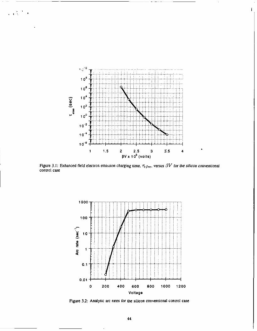
the numerical code discussed in Section 2.1.1 is used to determine refee over a range of
typically 5 values of /3V. The charging time ref,, is then plotted against /3V since the
analytic theory [9] indicates that -efee is a strong function of /3V. This plot is shown in
Fig. 3.1 for the control case over a relevant range. Times less than 1 x 10⁻⁸ sec are not
useful as that interval is on the order of a capacitor build-up time. Times greater than
1 x 10⁴sec are also not useful as either the ion charging time would dominate or the orbit
would be completed, causing the power system to regenerate. In the following property
variations, however, the same range of /3V is maintained where possible to simplify
comparisons.
Second, the analytical model discussed in Section 2.1.2 is used to determine the arc
rates. In this model, the arcing time is determined by the one emission site on a conductor
of typically 1000 sites which has the shortest charging time of all the cells. This is a
more realistic simulation than the numerical simulations in which only the effect of one
site on one conductor was studied. Hence, the effects determined by the numerical
simulations often do not have as much impact on the arc rate results as one might expect.
The experiment time is also a consideration, particularly for lower voltages where arcing
takes a longer time to occur. For the control case and the mitigation cases the experiment
43
1 0 ...... ......
10
100 .....
102
1 0 . . . .... .. 4 .
106 ..... ..: . . ....L..L -
100
1'A
1 1. . .
Voltage(vots
~~~~~Figure 3.1 2nane Al lcrnal misic n arc gin rates,,vrus3 for the silicon conventional cnrlcs
contrl c44

time is arbitrarily chosen to be one second. Also, arc rates are calculated at intervals of
-100V. The arcing rates for the control case are shown in Fig. 3.2. The curve clearly
shows the two dominating revions of e,q, and mo. At lower voltages, 7q, dominates
and the arc rate is a strong function of the voltage. At higher voltages, r,, limits the
arcing rate to the value determined by mission parameters, which is a weak function ofthe voltage. Consequently, the arc rate mitigation methods studied are intended to shift
and alter the slope of the 7ref, dominated region. The r7, dominated region can also be
shifted though it will remain at the same arc rate. The arc rate results are presented at
the end of the chapter in a separate section so that comparisons may be made among all
methods studied.
3.2 Interconnector Material
The work function of the electron emitting surface determines the ease with which elec-
trons are released. If the number of electrons emitted from the interconnector is-reduced,
the time for the electric field at the triple junction to build up will be increased. In
the analytical formula for 7ef,,, the work function determines the value of the Fowler-
Nordheim coefficients A and B given by Eqns. 1.8 and 1.9. Fig. 3.3 shows rTe, plottedagainst ,3V over a range of significant values for varying work functions. As expectedmetals with work functions higher than the control case of 4.76eV have longer times for
EFEE charging, and metals with lower work functions have shorter times.These numerical simulation results can easily be predicted -from the theory. To de-
termine the effect of a different work function t•,, we can solve the ratio refe( 4)w,)I
fe,•((Ok) usino Eqn. 1.7:
Tefee(4W 2 ) = exp ((A1.5 oI,5)6.53 x o09d\ (3.1)
-ref.e(OkW) ( fw2 up V-Rj- )The only unknown variable is q/, which is within the range 1.001-1.005 for emission
sites adjacent to the triple junction. For the cases shown in Fig. 3.3, this expression is
evaluated and plotted with the equivalent numerical values in Fig. 3.4. The predictions
are all within the margin of error for the analytical and numerical values, except for the
extreme case of Ow, =5.9eV which is predicted about an order of magnitude too high. Thisis therefore a useful tool for predicting the effect of changing the exposed interconnector
metal.
45

7 .. . .. . . .. . ... . .. . . . . .. .
10 . .Kovar (0 w=4.76eV)
p q: ; E Mn (0 w=4. I1eV)
1 0 -6.--Ag (0w=4.26eV)-4-Au (0w=5. 1eV)
* 10,
10
*0 10
........... .......
2.4 2.6 2.8 3 3.2 3.4 3.6OV x I e (volts)
Figure 3.3: Enhanced field electron emission charging time, ref,,, versus /3V for different work functions,Ow (eV) L *w=4. 1/0 w=4.76 Analytic -*w-5. 1/0 w-4.76 Analytic
-- O w-4.1/*w.4.76 Numeric --0- * w=6.1/0w-4.76 Numeric-,wi4.26/0 w.4.76 Analytic- w-5.9/0 w=4.76 Analytic
-A- w-4.26/ 0w-4.76 Numeric G8- 0 w=5.9/ 0w=4.76 Numeri
106.~~ ~~ .l*....h...4...4 .... 4 .... 4.. ................
10000
* 100
3 .. ..L.....
0.0
001 *.)~~~ .............4. .. b.. I.*..I 4
2.4 2.6 2.8 3 3.2 3.4 3.6PVX 10 (volts)
Figure 3.4: Analytic predictions and numerical results for TefeeITefee(Owta 4.76eV) versus f3V
46
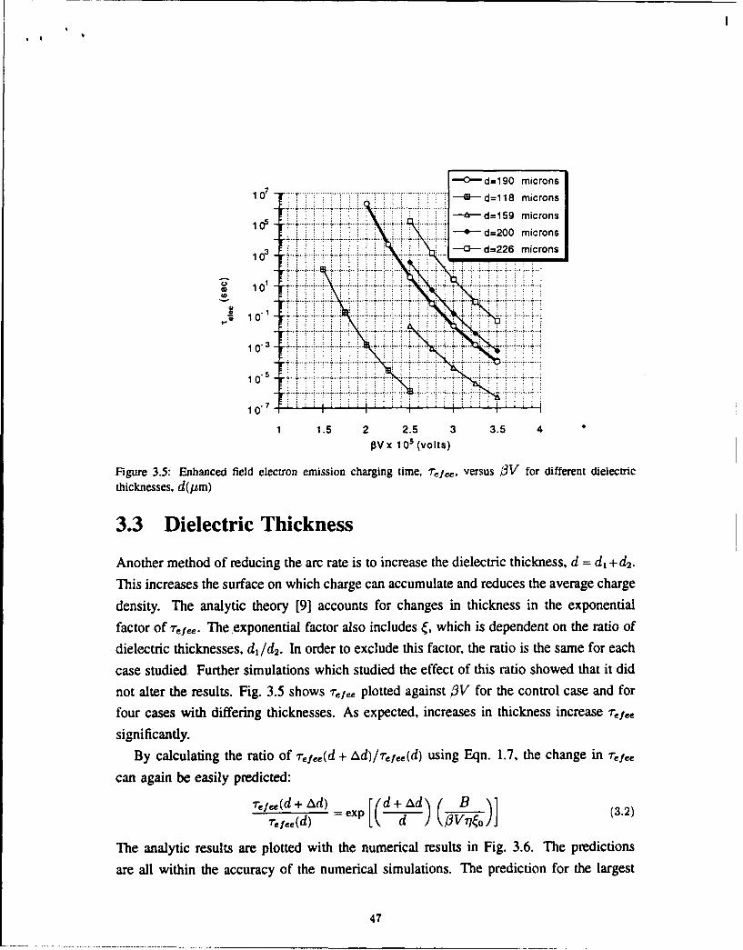
-Od= 190 microns
10. ' . ..........- d118 microns-6-d=159 microns
"-" -d=200 microns
.. ." " ....-- - d=226 microns
.0 -' . . . . . . . . . . . . . .. ..iii•""T :" "I '
1 0 .... ...
s 4. '..•..!. .i..... .. . .... ....... ...- .-+ . ...i..-..+ .
,o~ ~ ~~~~~ ~~~~~ .::::::::::::::::::: ::::::: ::::::: : . . . ... ............. .. . . . .o 10'
1 15 2 2.5 3 3.5 4lV x 10s (volts)
Figure 3.5: Enhanced field electron emission charging time, T efee, versus O3V for different dielectric
thicknesses, d(/Im)
3.3 Dielectric Thickness
Another method of reducing the arc rate is to increase the dielectric thickness, d = d, +d2.
This increases the surface on which charge can accumulate and reduces the average charge
density. The analytic theory [91 accounts for changes in thickness in the exponential
factor of Trefe. The exponential factor also includes ý, which is dependent on the ratio of
dielectric thicknesses, d1 /d 2. In order to exclude this factor, the ratio is the same for each
case studied Further simulations which studied the effect of this ratio showed that it did
not alter the results. Fig. 3.5 shows -efe plotted against OV for the control case and for
four cases with differing thicknesses. As expected, increases in thickness increase Tefee
significantly.
By calculating the ratio of rqfee(d + Ad)/r-,ee(d) using Eqn. 1.7, the change in Trefe
can again be easily predicted:
Te,,fe(d + ad) [d +ad) ( B (3.2)Teiee.(d) ex-p d 76
The analytic results are plotted with the numerical results in Fig. 3.6. The predictions
are all within the accuracy of the numerical simulations. The prediction for the largest
47
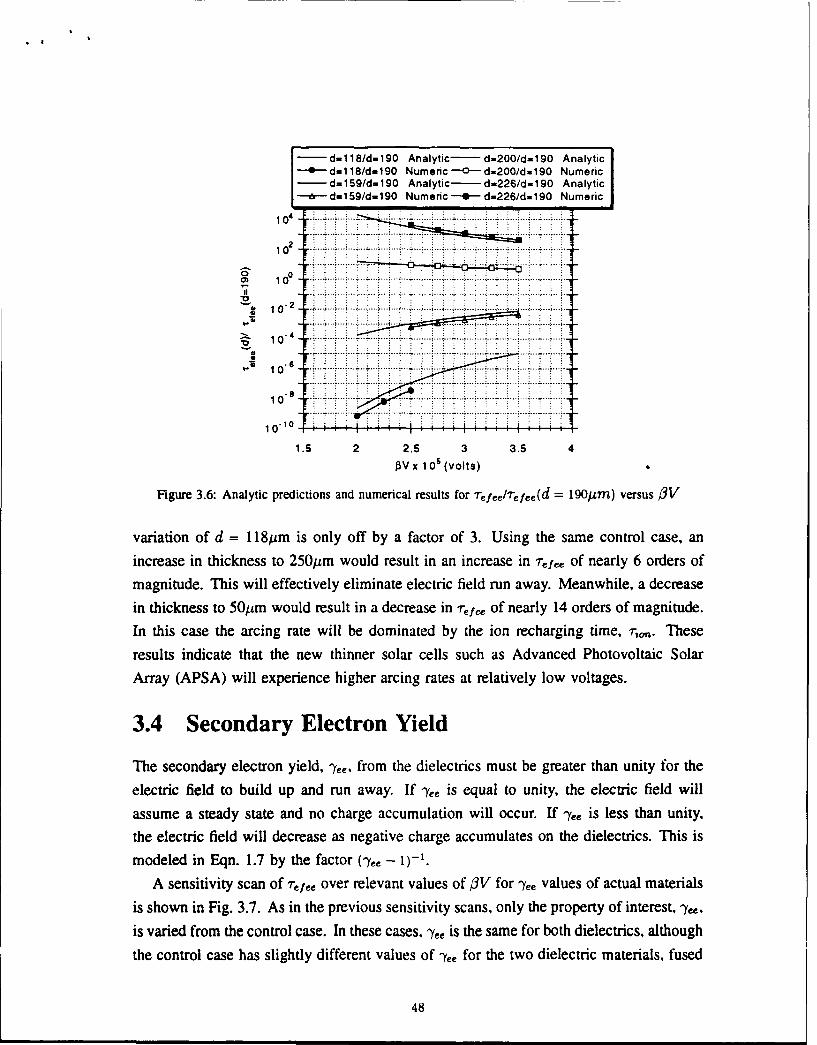
d- 118/d.190 Analytic- d-200/d=190 Analytic@- d=118/d=190 Numenc-O-c d=200/d=190 Numeric
-d=159/d=190 Analytic- d-226/d- 190 Analytica dI159/d.190 Numenc - d-226/d.190 Numeric
i02
............. .......... . . . . .. .
l op ,.- ,-- - -i ; .-. -, . -. , 3. ... . •.... ... . .. ... .. •....•. .... ..- . -• ., . .
....... . . .......
* = 1 0 -2 .................................... .• . i, ,-.--L - L - .- ! .- - - -.. ".". ' .. -.. ... - -•- - .. .....°...- --.
> 1 0 "4 ....... .. ...... ....... : : : : : : ......
108
10-10 l
1.5 2 2.5 3 3.5 4
V x 1 0 (volts)
Figure 3.6: Analytic predictions and numerical results for refee/lrefee(d = 190jtm) versus O3V
variation of d = 118pim is only off by a factor of 3. Using the same control case, an
increase in thickness to 250•m would result in an increase in rf,., of nearly 6 orders of
magnitude. This will effectively eliminate electric field run away. Meanwhile, a decrease
in thickness to 50,um would result in a decrease in Tefe of nearly 14 orders of magnitude.
In this case the arcing rate will be dominated by the ion recharging time, 7ro. Theseresults indicate that the new thinner solar cells such as Advanced Photovoltaic Solar
Array (APSA) will experience higher arcing rates at relatively low voltages.
3.4 Secondary Electron Yield
The secondary electron yield, %e, from the dielectrics must be greater than unity for the
electric field to build up and run away. If -ye is equal to unity, the electric field will
assume a steady state and no charge accumulation will occur. If Ne is less than unity,the electric field will decrease as negative charge accumulates on the dielectrics. This is
modeled in Eqn. 1.7 by the factor ( -e - '.
A sensitivity scan of refee over relevant values of 2V for -y values of actual materials
is shown in Fig. 3.7. As in the previous sensitivity scans, only the property of interest, -,
is varied from the control case. In these cases, -ye is the same for both dielectrics, although
the control case has slightly different values of -ee for the two dielectric materials, fused
48

i I I
-$----t]----h+-jt--l-j--OSi:'Yes- 7-.-- C:Yee=4-4.S
102 "''' BeO:Y ee-0.4-2.4
-0-- U: YeeO.4-2
-4 Cs:Yee-O.7-1.2
100 .. h .E E..... ... E...........0 1 0°
10.2
2.4 2.6 2.8 3 3.2 3.4 3.6
PV x 1 0s (volts)
Figure 3.7: Enhanced field electron emission charging time, refee, versus OV for different secondaryelectron yields, -yee
silica and DC 93500. In order to choose relevant values, the Eqn. 2.24 for -ye is evaluated
for different a'• d and E, values determined for actual materials. Since the ambient ion
charging is not calculated with secondary electron effects, the initial conditions for EFEE
charging are the same as for the control case for every f, variation. Consequently, d,
must only be known for the control case to determine y, for any other set of secondary
electron parameters. From the numerical simulation of the control case, d,- is 35.6tim, so
0, is estimated to be 890, and E, is estimated to be 75V. For the control case the estimated
"Yee is 15, but the numerical results showed -ye to be 7. In the other cases studied the
estimated values of -ye are also about a factor of 2 higher than the calculated values. The
lowest estimated value studied is N,, = 2.5 for cesium's properties, but the calculated
value is -ye = 0.7-1.2. The latter corresponds to the result of no electric field run away
by the numerical simulation. The results are shown in Fig. 3.7 with the numerical values
of -ye,. As expected, cases with secondary electron yields near unity have much longer
EFEE charging times, and the case (Cs) with -, values near and less than unity has an
infinite EFEE charging time since the electric field at the triple junction did not run away.
One difference between the analytical and numerical results is the effect of the dielec-
tric surface charge, which is not taken into account in the analytical model. As shown in
Fig. 3.8, the surface charge next to the triple junction is negative during EFEE charging
49
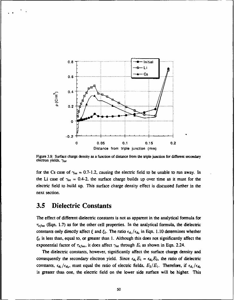
L i
0 .6 .. ..................
EC.,
-0.2
0 0.05 0.1 0.15 0.2Distance from triple junction (mm)
Figure 3.8: Surface charge density as a function of distance from the triple junction for different secondaryelectron yields, ^ee
for the Cs case of %Ye = 0.7-1.2, causing the electric field to be unable to run away. Inthe Li case of Ne = 0.4-2, the surface charge builds up over time as it must for the
electric field to build up. This surface charge density effect is discussed further in the
next section.
3.5 Dielectric Constants
The effect of different dielectric constants is not as apparent in the analytical formula for
"T-hfe (Eqn. 1.7) as for the other cell properties. In the analytical formula, the dielectricconstants only directly affect C and Co. The ratio Ed,/efd in Eqn. 1.10 determines whether
ýo is less than, equal to, or greater than 1. Although this does not significantly affect theexponential factor of refe, it does affect -y, through E1 as shown in Eqn. 2.24.
The dielectric constants, however, significantly affect the surface charge density and
consequently the secondary electron yield. Since ed, El = e 12E2, the ratio of dielectric
constants, Ed, /f,, must equal the ratio of electric fields, E2/E1 . Therefore, if (d,/f/2
is greater than one, the electric field on the lower side surface will be higher. This
50
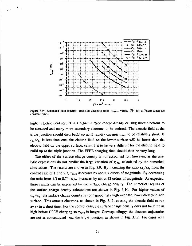
1013 * -. O- * - Ed1/ Sd2=1.3So " ..i--i--i.-.i.-.i ..- ..-- .. -- - -.... -- •• • . .. . . .. . . . . . ............... . . ... .. .d l/•Ed 2=2.7
10 1...... . Edl/- Ed2=1l110. " --- Edl/Ed2=-.74
I . .OP . :.. .- .. -.- . . -. . -- ..? ..-..-. .. . ......
• - ..- ..-- ..-- . . ... .. .. .. ... .. .. ...'-° - ---- .-÷-- +°---
= ,~.•-----.i.-..... ... - - .....---..-... . ....... ." °"°1 . , , , , ... ..... .. ....So • i•...•.• i..i.•.• +•. .•.• •.. .. ...•.•....i .i •.•.•. .. •.. ... ....... H
ox10, .volts)
10-
16 15 2 25 . 3. .4
OVX 1 05 (volts)
Figure 3.9: Enhanced field electron emission charging time, -"efee, versus )3V for different dielectricconstant ratios
higher electric field results in a higher surface charge density causing more electrons to
be attracted and many more secondary electrons to be emitted. The electric field at the
triple junction should then build up quite rapidly causing efe,, to be relatively short. If
Ed, /f4 is less than one, the electric field on the lower surface will be lower than the
electric field on the upper surface, causing it to be very difficult for the electric field to
build up at the triple junction. The EFEE charging time should then be very long.
The effect of the surface charge density is not accounted for, however, as the ana-
lytic expressions do not predict the large variation of refe calculated by the numerical
simulations. The results are shown in Fig. 3.9. By increasing the ratio Ed•3 /•, from the
control case of 1.3 to 2.7, rf,,, decreases by about 7 orders of magnitude. By decreasing
the ratio from 1.3 to 0.74, refe increases by about 12 orders of magnitude. As expected,
these results can be explained by the surface charge density. The numerical results of
the surface charge density calculations are shown in Fig. 3.10. For higher values of
fd, /ed, the surface charge density is correspondingly high over the lower dielectric side
surface. This attracts electrons, as shown in Fig. 3.11, causing the electric field to run
away in a short time. For the control case, the surface charge density does not build up as
high before EFEE charging so Tefee• is longer. Correspondingly, the electron trajectories
are not as concentrated near the triple junction, as shown in Fig. 3.12. For cases with
51
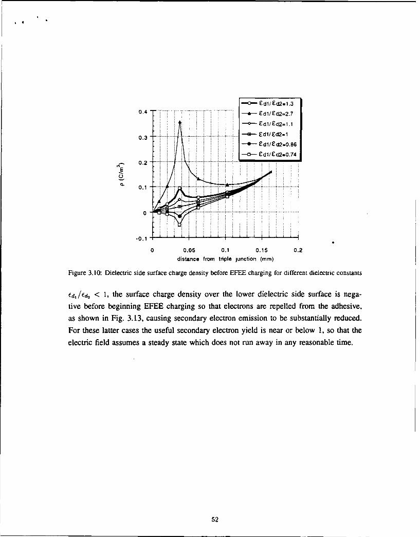
. I
SEwiEd2=1.304 -a--- Ed,/Ed2-2.7
-in- Edl/Ed2-10 .3 ......;.... .. .... ; .•..... .. : .... .......•. : d /E 2
-. e--Edl/Ed2,,O.86
03
-a- dlfEd2-0.74
0.1
0
0 0.05 0.1 0.15 0.2distance from triple junction (mm)
Figure 3.10: Dielectric side surface charge density before EFEE charging for different dielectric constants
Ed, /E4 < 1, the surface charge density over the lower dielectric side surface is nega-tive before beginning EFEE charging so that electrons are repelled from the adhesive,
as shown in Fig. 3.13, causing secondary electron emission to be substantially reduced.
For these latter cases the useful secondary electron yield is near or below 1, so that the
electric field assumes a steady state which does not run away in any reasonable time.
52
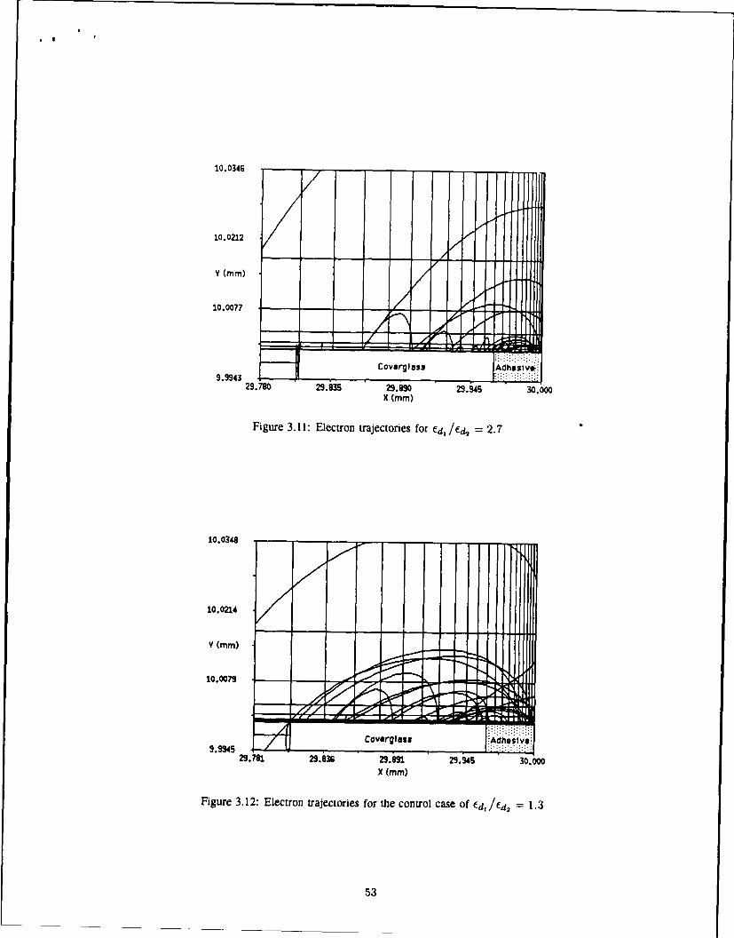
10.0346
10.0212
V (mm)
10.0077 - - - - - -
Coverglass Adhesive.'.:9.9943
29.780 29.835 29.890 29.A45 30.000X (mm)
Figure 3.11: Electron trajectories for Ed,/Ed, = 2.7
10.0348
10.0214
Y (mm)
10.0079 .
9.9545 29.M8 29.836 29.m5 29.A4S 30.000
X (mm)
Figure 3.12: Electron trajectories for the control case of Ed, •d, = 1.3
53

10.0355
10.0218
Y (Mm
10.008M0
Coverglass :Adhesive:9.9942
29.780 29.835 29.990 29.9ý45 30.0'00X (MM)
Figure 3.13: Electron trajectories for Ed, lfd2 =- 0.74
The effects on the secondary electron yield as calculated by the numerical simulations
can be seen in Fig. 3.14. As expected from the surface charge density results, -ye, for
cases with Cd, /Qd2 < i is significantly lower than for the other cases.
3.6 Overhanging the Covergiass
The final mitigation strategy studied involves lengthening the coverglass into an overhaii-
over the interconnector to create a back surface, as shown in Fig. 3.15, on which charge
can accumulate. This method was expected to increase ref,, since the overhang creates
an additional surface over which the charge must build up for the electric field to run
away.
3.6.1 Numerical Results
As shown in Fig. 3.16, the results confirm this expectation. As the overhang is incro-ased
in length up to 30,4m, 7-f, is increased uniformly. in the O3V range studied, this pattern
changes for overhangs longer than 3O0Am, indicating a different physical effcct of the
overhang on the EFFE charging time.
The difference between these two classes is clearly shown in Fig. 3.17. The electric
field at the tripbý junction ETJ increases with time for the the first class, indicating a
54

8 ... :'"''" ''" . . SEd1/Ed2=1.3
87 ........ .................... ........ . . ................
* -- 0- Edl/,d2=1.1
0 0 - u- 5 o/Ed2-1.1
0a E4 d1IcZd2-0.86.>. 5 ............... .. : : : + l"0 /Ed2-I.04
4" 6.........'' : : ' ' ' " " ' " ... . ........
3 ... . ... -7 : ...... . .. .. . .. .....:.....
2 -7': ............................... ..........--.-- ...d/ ........3 40
3
10.' 10 10a 10. 2 100 1l2 10' 106 108 101° 1012
time (sec)
Figure 3.14: Average secondary electron yield over the adhesive versus time for different dielectric con-stants
Coverglass Overhang
7X-Coverglass_ _'A d h eI siv-Adesv
"Triple Junction
Figure 3.15: Model of coverglass overhang
55

ii
101.......... -~--0 no ove rha ng
10 10 microns014
1012 3.. ... 50 microns
10 0 75 microns
CD 108....... .... . . ...
: 16
10
10.2
10 .... .1 . .
2 2.5 3 3.5 . . 4.51v x . . (volts)
Figure 3.16: Enhanced field electron emission charging time. T"efee, versus /3V for different overhanglengths
build up of charge due to EFEE and secondary electron emission. However, it decreases
initially before increasing, often drastically, for the second class, indicating an inital
build up of negative charge from electron accumulation before electron emission from
the side surface becomes high enough to create the positive charge build up necessary
for runaway.
The corresponding effects of these differing electric fields on the electron trajectories
can be seen in Figs. 3.18 and 3.19. The first shows that the electrons in the first class
of simulations are merely diverted by the overhang. The second shows that the electrons
in the second class are mainly confined to the back surface with few arriving at the
side surface of the coverglass. This shows that the first class of overhangs are acting as
additional surface area while the second class are obstructing the electron trajectories to
the side surface.The potential along the surface reflects these electron trajectories. Fig. 3.20 shows that
for the first class the potential along the back surface increases with time, which causes
the electric field at the triple junction to increase with time as well. For the second
class, shown in Fig. 3.21, the back surface potential initially decreases with time until
it eventually increases at very larg,. times. This initial potential decrease corresponds to
56

6 10-micron overhang3.1 10 .... . . 50-micron overhang .
3 .0 1 0 6 - ......................................... .................................................... ................
0-_ 2 . 6 .................. .. .... ........ ........... .... ................. ................ ................. 4, .. ............S2.9 10
2 7 1 6 .............. .... ........ ................ ................. ................ .................. 1................. ."' 2.8 10.
6S 2 .7 1 0 ............... .. ........ ..... ; ....... . . ......... . ... . .... ............
LL 2 .6 1 o0 .......... ............ .... . ....... .... ............ ........ , ........ ........... •~- 2.6 10 -
10`4 0.01 1 10 2
Time (sec)
Figure 3.17: Class comparison of 7-efee versus ETj for kJV = 3.5x10 5 V
10.0259 -
10.0167
Y (mm) I/. •/, -
10.0075
coverglass
9.992adhesive23.790 29.93S 298M 29.i44 29.
X (mm)
Figure 3.18: Electron trajectories for 101im overhang; 3V = 3x 10⁵ V
57
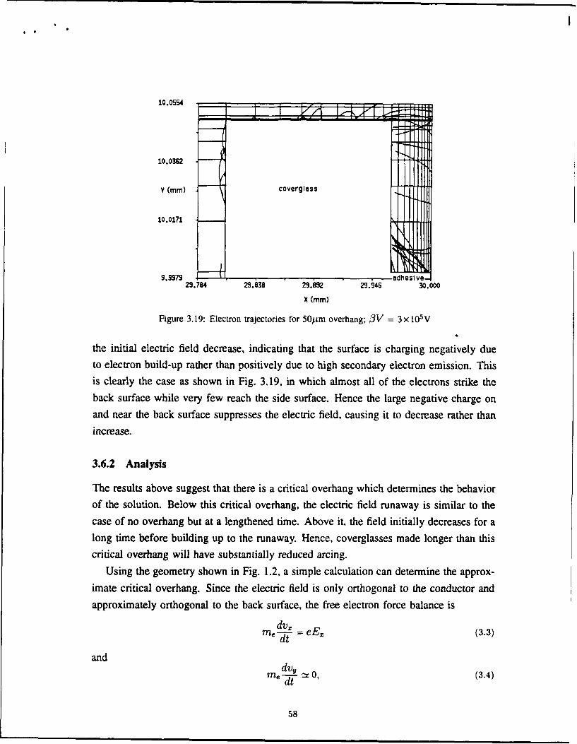
10.0554
10.0362
Y (mM) covergless
10.0171
9.9979 ". edhesive-29.784 29.i38 29.892 2.946 30.000
X (Mm)
Figure 3.19: Electron trajectories for 50Atm overhang; OV = 3 x 10⁵V
the initial electric field decrease, indicating that the surface is charging negatively dueto electron build-up rather than positively due to high secondary electron emission. This
is clearly the case as shown in Fig. 3.19, in which almost all of the electrons strike the
back surface while very few reach the side surface. Hence the large negative charge on
and near the back surface suppresses the electric field, causing it to decrease rather than
increase.
3.6.2 Analysis
The results above suggest that there is a critical overhang which determines the behavior
of the solution. Below this critical overhang, the electric field runaway is similar to the
case of no overhang but at a lengthened time. Above it, the field initially decreases for a
long time before building up to the runaway. Hence, coverglasses made longer than this
critical overhang will have substantially reduced arcing.
Using the geometry shown in Fig. 1.2, a simple calculation can determine the approx-
imate critical overhang. Since the electric field is only orthogonal to the conductor and
approximately orthogonal to the back surface, the free electron force balance isdv,
m,--- - = eE. (3.3)
andrdvy (3.4)
dv
58
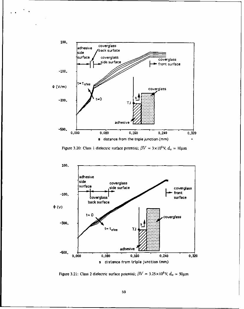
100.
adhesive coverglass
side /back surface
surface / coverglass ergassiesurface front surface
"-100. cov
t=lefee /J€ (V/m) coverglass
-300. , i
0.. 000 080 O. 0.10 0.24I0 0.320
s distance from the triple junction.(mm)
Figure 3.20: Class 1 dielectric surface potential; 3V 3 x 1O5V, d, = 10om
100.
adhesiveside coverglasssurface side surface coverglass
""00 front-10 loverglass' surfaceback surfaces
0(V)
t0.....- coverglass
-300. ,
adhesive ....
0.000 0.0oio 0160 0.240 0.320s distance from triple junction (mm)
Figure 3.21: Class 2 dielectric surface potential; OV = 3.25x 10⁵ V, do = 50pm
59
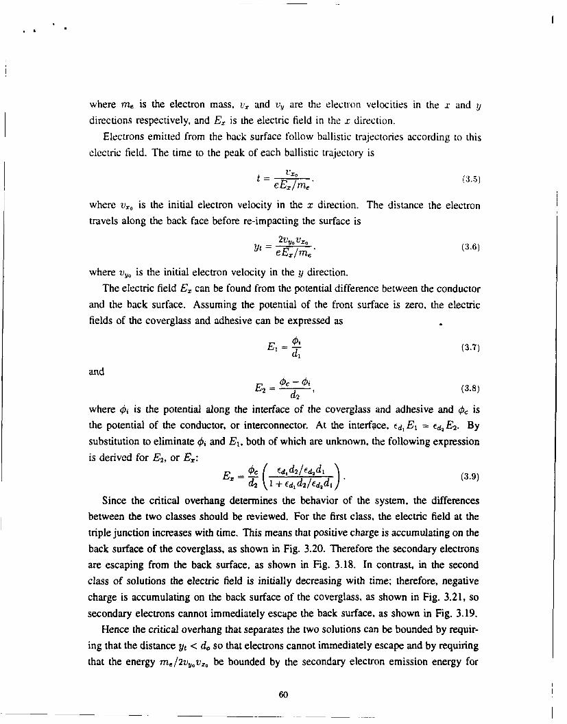
, S
where m, is the electron mass, v, and v, are the electron velocities in the x and y
directions respectively, and E. is the electric field in the x direction.
Electrons emitted from the back surface follow ballistic trajectories according to this
electric field. The time to the peak of each ballistic trajectory is
eE/m" (3.5)
where Vo is the initial electron velocity in the x direction. The distance the electron
travels along the back face before re-impacting the surface is
2v 0 L'ro0 (3.6)
eE,/m,'
where vyo is the initial electron velocity in the y direction.
The electric field E, can be found from the potential difference between the conductor
and the back surface. Assuming the potential of the front surface is zero, the electric
fields of the coverglass and adhesive can be expressed as
E, = d't (3.7)
and ttc - c¢,E2 = d-(3.8)
where q, is the potential along the interface of the coverglass and adhesive and Oc is
the potential of the conductor, or interconnector. At the interface, ,d E, = fd E2. By
substitution to eliminate O, and El, both of which are unknown, the following expression
is derived for E2, or E.:
EX • fd1 ,d2/Ed.,d " (3.9)d2 + 1Ed~d2/Ed,,dl) . 39
Since the critical overhang determines the behavior of the system, the differencesbetween the two classes should be reviewed. For the first class, the electric field at the
triple junction increases with time. This means that positive charge is accumulating on the
back surface of the coverglass, as shown in Fig. 3.20. Therefore the secondary electrons
are escaping from the back surface, as shown in Fig. 3.18. In contrast, in the second
class of solutions the electric field is initially decreasing with time; therefore, negative
charge is accumulating on the back surface of the coverglass, as shown in Fig. 3.21, so
secondary electrons cannot immediately escape the back surface, as shown in Fig. 3.19.
Hence the critical overhang that separates the two solutions can be bounded by requir-
ing that the distance yt < d, so that electrons cannot immediately escape and by requiring
that the energy m,/2vt°,vr be bounded by the secondary electron emission energy for
60

o tg
unity yield, C1. This latter requirement means that an electron striking the back surface
never has enough energy to release more than one electron. Therefore, the back surface
must charge negatively. These two bounds give
d'o < 4EI 1 + (d, d2/Ed 2 did2- eo, (d,/ d~dl (3d.10)
For the conditions in Table 3.1, .61 40eV and with 0, = 400V, Eqn. 3.10 gives dc <
67pim. 1This corresponds well with what is observed in Fig. 3.16 where the 50Lm over-
hang shows the characteristics of both classes while the 7 5 1im overhang shows only the
characteristic of the second class.
This approximate expression can be further simplified in the limit d2 < d, (which is
usually the case). Eqn. 3.10 then simplies tod - < 4E1d"d (3.11)
0 - e~fcd, "
This shows that one can obtain the smallest critical overhang by reducing di -as much
as possible, consistent of course with the need to maintain radiation protection, and by
modifying the secondary electron emission properties of the covergiass so as to reduce
the energy at which the yield is unity.
3.7 Arc Rate Results
The arc rates are determined by using the analytical model discussed in Section 2.1.2, as
explained for the control case. This model is limited by the analytic expressions, which
are only approximations of real processes and effects. For the results in the previous
section which are consistent with the analytic predictions, the model is used with the
varying parameters. For the secondary electron yield, dielectric constant, and overhang
effects on "rf;,, which are not fully accounted for in the analytic expression, the model
is used with 'ref modified according to the results from the numerical simulations.
The results are shown in Figs. 3.22-3.26. In all cases the curves saturate around
350sec-', where the arc rate is limited by r,. which is not as dependent on voltage as
is rfee. The goal of the mitigation strategies can clearly be seen, then, as increasing the
voltage range of T e,-• dominance.
The effect of different work functions on the arc rate is shown in Fig. 3.22. None of
the work functions significantly affect the arc rate, although the higher work functions
do not arc at -200V. Also, little difference is seen between the arc rates of commonly
used Kovar and silver interconnectors.
61
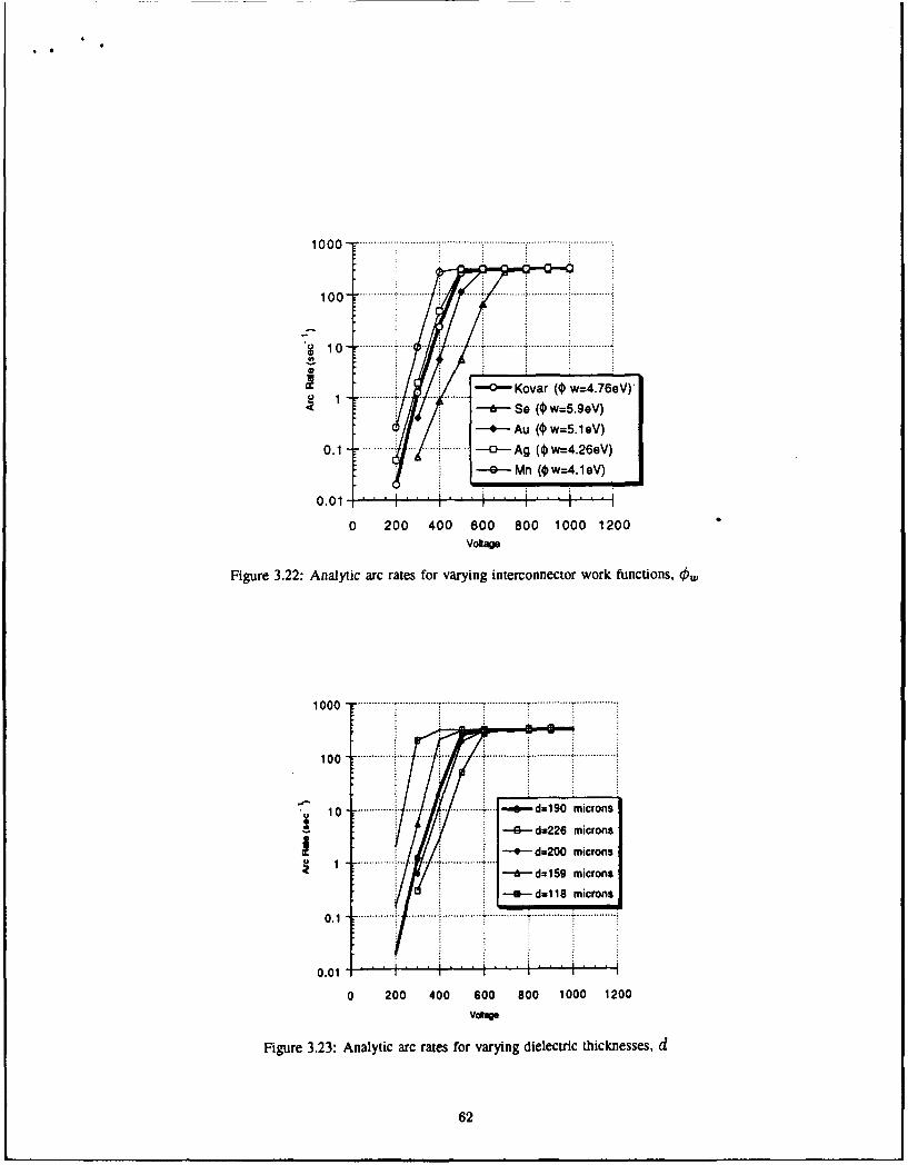
100-
0 Kovar (~w=4.76eV)'1~ So (O w=5.9eV)
-4--Au (0) w=5.1leV)0.1 -0 Ag (0 w=4.26eV)
-0-Mn (40 w=4.1 9V)
0.01-+.L
0 200 400 600 800 1000 1200Vokage
Figure 3.22: Analytic arc rates for varying interconnector work functions, 4
100.... ...................-.........
10 .............. ........ -. *.--d=190 microns-1- dz226 microns-.. dz200 microns
6 -d=159 microns
a4-d=llS microns
0.1
0.01 - ------0 200 400 600 800 1000 1200
VOlage
Figure 3.23: Analytic arc rates for varying dielectric thicknesses,d
62

io
| o 3 .-- .-- - .... .. .. .....W .-.-- -- . ......-7----..-. .. ....... ... .. .. . .. .. . .. .. .. .. .. ..
a- 10•
-0 .• ....•... -.... ..... . .. .. •... . ... . -i ..•. ..... .... .. ... .
a -0Si: )fae7
8 LC: Y ee=4-42510- ~ ~ .. .. ..... 6 B :Yee--0.42.3~~ 10- UL: Yee=0.42
) - Cs:Yee=0.7-12
1 0 -.. . . .. .
0 200 400 600 800 1000 1200
Voltage
Figure 3.24: Predicted arc rates for varying secondary electron yields, 'Yee
The thickness variations show a greater effect on the arc rate, especially for thesmaller thicknesses between -200V to -400V. For a 118pm thickness of the coverglass
and adhesive dielectrics, the arc rate is almost saturated at -300V, while the control casethickness of 190gm does not saturate until -600V. Increasing the thickness to 200/m oreven 226gm eliminates arcing at -200V but does not reduce arcing significantly at highervoltages.
The effect of th5" secondary electron yield on the arc rate is shown to be significantonly when the electric field does not run away, as in the N, = 0.7-1.2 case. Even forthe two cases (BeO and Li) which have secondary electron yields near and below unity,
the arc rate is just barely reduced from the control case. Any secondary electron yieldnot near unity, such as that of carbon ('/e = 4-4.5), did not change the arcing rates at all
from the control case of -y,, = 7.
The dielectric constant variations and coverglass overhang cases show the largest effect
on the arc rate. For the Ed,/f,, = 2.7 case, the arc rate is almost saturated at -300V. Forthe case of equal dielectric constants, however, the arc rate does not saturate until -900V.For variations of fd,/I,4 < i the arc rate is reduced significantly. No arcing is predicted
until -600V for the fd, /E, 2 = 0.74 case.For the coverglass overhang arc rates, the two different classes can be seen clearly in
Fig. 3.26. The arc rates of the first class do not decrease much even with an overhang
63

S 4I
-'--E dl/Ed2-2.7 - E dl/ .d2=1100 .. •..CEdl/Ed2,,1.1 C dl1/ E.d2=0.74
S E ddl/Sd2=1.E d l/E d2-0.86
1000
1 0 0 ..... .. ........ .... .... ....... .. ...... ...* . I , il. 1. 0 . . ................... ......... .. ................. .
0.01
0 200 400 600 800 1000 1200
Voltage
Figure 3.25: Predicted arc rates for varying dielectric constant ratios, d, /Ed,
of 30,rm, but the arc rates of the second class are significantly reduced. The 75,4m case,which is beyond the critical overhang for the cell studied, shows no arcing until -600V
and does not reach the saturation level in the range of voltages examined.
These predictions will be tested in the upcoming Air Force Photovoltaic and SpacePower Plus Diagnosics (PASP Plus) space experiment and the NASA Space Shuttle
SAMPLE flight which will overhang the coverglass as well as apply a coating over the
triple junction. These experiments are discussed in the next chapter.
64
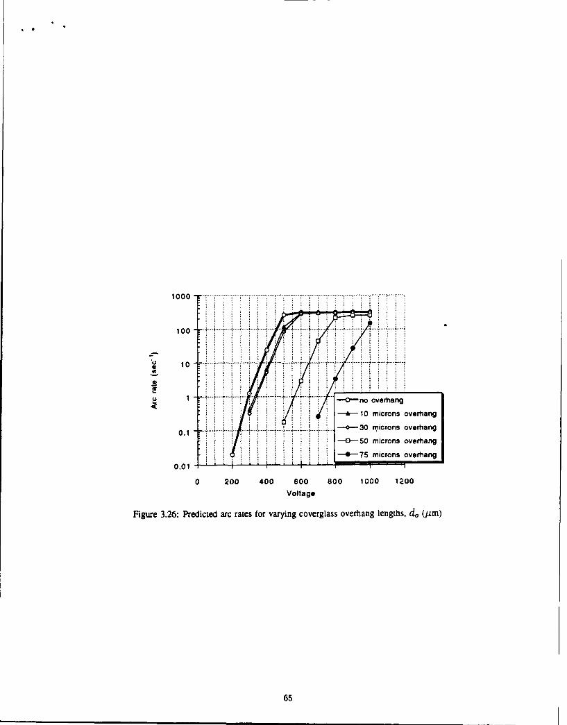
10 0 0 -....... ...........................
1oo~ ~~. 'i i i"iiii ..... ... .. .. .. ... ~ii ..1 7 -0*-no overhang
f10 microns overhang
01 30 microns overhang
0 -.1 -' ..r" - " ........
---- 50 microns overhang
-- 75 microns overhang
0.01 - J
0 200 400 600 800 1000 1200
Voltage
Figure 3.26: Predicted arc rates for varying coverglass overhang lengths, do (/Im)
65

Chapter 4
PASP Plus and SAMPIE Predictions
In the next few years, four space missions are planned to study high voltage solar ar-
rays. Two of these are the Photovoltaic and Space Power Plus Diagnostics (PASP Plus)
experiment and the Solar Array Module Plasma Interactions Experiment (SAMPIE). By
using the numerical and analytical models for the conventional and wrap-through-contact
cells, arcing predictions can be made for these missions to aid in their preparation and
to further check the validity of these models.
4.1 PASP Plus
PASP Plus is designed to provide the Air Force with important information regarding
higher power space systems. Since greater spacecraft power will be required, the Air
Force anticipates using advanced high voltage solar arrays and power distribution systems.
The environmental interaction hazards of these systems therefore need to be determined
to improve the reliability of future missions. To accomplish its task, the PASP Plus
experiment includes both advanced solar arrays and a number of diagnostic instruments.
PASP Plus has four main objectives[201:
(1) characterize the electrical performance and the environmental interaction of
advanced solar array designs operating at high voltages in the ionosphere and
magnetosphere;
(2) determine the long-term radiation degradation effects of several advanced solar
arrays;
(3) determine the impact of the space environment on solar array operation for various
solar cell technologies; and
(4) obtain flight performance data for advanced array designs never before flown.
66
Q II
4.1.1 Experiment Description
The PASP Plus experiment will be flown on the Advanced Photovoltaic and Electronics
Experiments (APEX) satellite, scheduled to be launched in the summer of 1993 aboard
the Pegasus launch vehicle. The satellite should reach an orbit of 1850km apogee, 350km
perigee, and 70' inclination. This polar orbit allows the payload to be continuously sun
pointing. The experiment is expected to last one year minimum and three years nominal.
The APEX spacecraft in its deployed configuration is shown in Fig. 4.1. The arrays
are located on the top shelf and on one of the deployed panels. The other three panels
are the solar arrays needed for the spacecraft power system. Beneath the payload shelf
is the avionics shelf, where most of the diagnostic instruments are located. There are
three types of sensors to obtain array performance data and five types of sensors to
characterize the space environment around the spacecraft. To calibrate the performance
of the solar arrays, the following instruments will be used: a sun sensor to measure
the incidence angle, meters to measure the current and voltage, and sensors aear each
array to measure the temperature. Instruments which characterize the space environment
include a transient pulse monitor for measuring electromagnetic interference, a langmuir
probe with sense potential capability for measuring the thermal plasma temperature and
density, a dosimeter for measuring ion and electron radiation, an electrostatic analyzer
to determine electron and ion spectra of moderate energy (10eV - 30keV), and five
monitors for determining the amount of degradation due to radiation and the amount due
to contamination. The spacecraft also contains a voltage generator capable of biasing the
arrays at multiple high voltage levels, an electron emitter which will enable the satellite's
potential to be altered, and an electronics controller for satellite operation.
Seventeen arrays of twelve different types will be mounted on the payload shelf and
the deployed panel. Since there are only 16 electrical channels, one of the arrays will not
be used. Ten of these arrays will be subject to multiple voltage biasing. The arrays, as
well as the instruments described above, are all numbered for identification. They will be
therefore introduced in order of their instrument numbers, and the biased arrays will then
be described in further detail, with the exception of the concentrator arrays which are not
included in this research. Arrays #0, #1, and #2 contain silicon conventional cells. The
silicon WTC cells designed for Space Station Freedom make up array #3. Arrays #4 - #6
are Applied Solar Energy Corporation's (ASEC) gallium arsenide/germanium (GaAs/Ge)
conventional cells, but array #5 will not be used so that its channel can be used by the
APSA cell array. The advanced solar cells of AIGaAs/GaAs Monolithic MBG are on
array #7. Spectrolab's WTC GaAs/Ge cells are located on array #8. Array #9 contains
67

Figure 4.1: Deployed APEX spacecraft with PASP Plus experiment payload
the amorphous silicon cells developed by TRW and Solarex. Another advanced solar
cell, indium phosphate (InP), is on array #10. The conventional GaAs/Ge cells made by
Spectrolab are on array #11. Another MBG cell, Boeing's GaAs/CuInSe solar cell, make
up arrays #12 and #13. The Mini-Cassegrainian GaAs cell created at TRW will be on
array #14 to accompany the newer Mini-Dome Fresnel Concentrator created at Boeing
which is on array #15. Finally, the APSA cell was added late to the list so its array is
#36.
The silicon conventional arrays #1 and #2 are the first biased arrays, containing 10
and 20 cells respectively. Originally built by RCA in 1984, these cells are included
to be representative of present operational space flight solar cells. Also, they were not
designed to withstand high voltage operation. The cells are 2cm x4cm and 203/rm (8mil)
thick. The coverglass is fused silica and the cover adhesive is DC 93500, of estimated
thickness 153pm (3mil) and 37jim (1.Smil) respectively. The interconnector is assumed
to be Kovar, which has an estimated work function 4.76eV.
The Space Station Freedom array of 4 cells (#3) will also be biased. These WTC
cells were designed to operate in low earth orbit at a 160V nominal operating voltage.
The 8cmx8cm cells are 203pm (8mil) thick. As discussed in Section 2.2. the cells are
68

covered with a ceria-doped borosilicate..coverglass and a Kapton substrate.
Arrays #4 and #6 of ASEC's GaAs/Ge conventional cell design are comprised of 20
and 12 cells respectively, and both will be biased. These cells were designed to have high
radiation resistance and high cell efficiency, making them representative of the standard
for the next generation of satellite photovoltaic power. The 4cmx4cm cells have a
thickness of 76jLm (3.5mil) and CMX coverglasses of 102,tm (4mil). The interconnector
is silver-plated invar so the relevant work function is that of silver, which is 4.26eV.
Both of Spectrolab's arrays, #8 and #11, will be biased. The first array is their WTC
design, which is expected to operate better than conventional cell designs at high voltages.
The 4cmx4cm cells, which are 1771im (7mil) thick, are covered by a 152,um (6mil) thick
coverglass and mounted on a Ge substrate. The second array contains a similar cell of
conventional design. The dimensions of both the cell and coverglass are the same, and
the adhesive is estimated to be 761Lm (3mil) thick. Like the ASEC GaAs/Ge cells, these
cells also have a silver-plated invar interconnector.
The Advanced Photovoltaic Solar Array (APSA) is the final high voltage biased array
studied. These thin-film silicon cells are expected to be the cells of the future, based on
the mass cost savings they yield. Built by TRW, they are 2.6cmx5.lcm of only 56pm
(2.2mil) thickness. More importantly for arcing considerations, the cell CMX coverglass
thickness is merely 51)im (2mil) thick and the DC 93500 cover adhesive is estimated to
be 76Pm (3mil) thick. The interconnector is again silver-plated invar.
The voltage biasing will be performed in pre-set sequences from -500V to +500V,
usually in increments of 25V. Each voltage level will be maintained for twenty seconds
so that the array can attain steady state conditions.
4.1.2 Predictions
To predict the arcing rate of the biased arrays, the analytic arc rate method described in
Section 2.1.2 is used. Table 4.1 shows the given and assumed cell properties necessary
for the arc rate calculations. To determine Cde,,, and the offset of 7ef,. due to the surface
charge density (see Section 3.4), the numerical model must be run initially. Only the
first scheme, the capacitance matrix method, is necessary to determine the polynomial fit
for Cdi,•,. Since the surface charge density is not incorporated into the analytic model,
an offset of reiee(numerical) versus rf,, (analytical) must be accounted for. The case
chosen by Cho [3] closely matches the numerical and analytical TfLe values. Since Trefe
versus WV curves have the same shape, the best technique is to determine the offset of
each curve from the case that can be accurately predicted analytically. Therefore, the
69

Table 4.1: PASP Plus data used for arc rate predictions
Instrument No. 1, 2 3 4, 6 8 11 36
Cell Type Si Si WTC GaAs/Ge GaAs/Ge WTC GaAs/Ge APSA
Manufacturer RCA NASA ASEC Spectrolab Spectrolab TRW
Cell Size (cm2 ) 2x4 8x8 4x4 4x4 4x4 2.6x5. INo. of Cells 20,60 4 20, 12 4 8 12
Cell Gap (jim) 500 1000 500 1000 500 635
d,11 (jim) 203 203 89 178 178 56
d, (4m) 153 203 102 152 152 51
d 2 (WiM) 37 N/A 51 N/A 76 76
CE, 3.5 4 4 4 4 4
•d 2 2.7 3 2.7 3 2.7 2.7
^,-,axi 3.46 4 4 4 4 4
7,-,ax 3 2 3 2 3 3
E., (eV) 330 400 400 400 400 400
E•2 (eV) 300 200 300 200 300 300
0, (eV) 4.76 4.85 4.26 4.5 4.26 4.26
entire numerical model is used at a specified voltage with the orbit integration scheme
run for several 3 values, typically five, to determine this offset.
The orbital data for the analytical model requires a different approach. Since the orbit
is neither circular nor of constant altitude, the orbital parameters must be determined for
each point along the orbit at which the arc rate is to be calculated. The International
Reference Ionosphere (IRI) program, developed at Goddard Space Flight Center in June
1987, can calculate the ambient density ne, the electron temperature T, and the ion mass
m, if given the altitude, month, hour, sunspot number, and the geodetic coordinates.
Since the exact time of the biasing is unknown, the parameters are averaged over the
entire year by hour and by month. The times that gave the lowest and highest ambient
densities ire also used to define the lowest and highest arcing rates which might be
observed. The variation due to different sunspot numbers is within the variation due
to ambient densities. To determine the coordinates, as well as the altitude and orbital
velocity, a separate calculation is necessary. Orbital mechanics are used to find the state
vector in inertial coordinates of a given altitude. These are then converted to the earth-
fixed coordinates. By using the orbit inclination, longitude of the ascending node and
70

* g
the orbital eccentricity, the equations of motion can be integrated using a fourth-order
Runge-Kutta method to obtain other positions along the orbit.
At altitudes higher than 1000km, the IRI model is useless for obtaining particle den-
sities. At these altitudes, however, the following formula developed by Al'Pert [11 has
been shown to agree well with experimental measurements:
he(z) :: neo-:- exp +~ R+In .(4.1)z 2kTo [+~ 1-o"Z
In this equation Ro is the Earth's mean radius, no is the electron density at 1000km, g0
is the gravitational acceleration at 1000km, M, is the mass of hydrogen at 1000km, To
is the electron temperature at 1000km, and zo is the altitude of 1000km. Finally, the arc
rate program requires the input of a range of electron densities. Since each voltage bias
will be held for 20sec, the electron densities at either end of that range along the orbit
are used to define the maximum and minimum densities expected.
For each array arc rates are predicted for voltages up to -500V in 25V increments at
intervals of 600sec around the orbit. Near apogee, the spacecraft slows and the arcing
rates have less variation due to the lower ambient densities so the intervals are increased
to 1200sec.
The arc rate results for the conventional arrays are presented in Figs. 4.2-4.13. For
each array, the first figure shows representative arc rates around the spacecraft orbit for
the entire voltage range. Standard deviation error bars included on these figures are based
on typically 100 calculations for each voltage. The arc rates at lower voltage biases are
identical since r'f,, is dominant. The diverging curves at higher voltages indicate 7jm is
beginning to affect the arc rates. To distinguish the arc rates at these higher voltages, a
second figure for each array shows all of the arc rate curves in the r,, range. As shown
in Fig. 4.2, the arc rates for the silicon conventional array with 20 cells range from an
average of 0.004sec-I at 200V to 21 lsec-I at 500V. At 500V bias, the arcing rates are as
low as 8.75sec- 1 , which is calculated at apogee. The addition of 40 more solar cells to
the array increases the number of emission sites where arcing can occur, thus decreasing
the time between arcs. This is clearly seen in Fig. 4.4, which shows that arcing begins
at voltages as low as 175V for array #2. The highest arcing rate calculated is 366sec-'
at perigee for a voltage bias of 500V, while at apogee the arcing rate is 33sec-'. For
ASEC's GaAs/Ge array of 20 cells (#4), arcing is predicted at 125V, as shown in Fig. 4.6.
Accordingly, the arcing rates are much higher at 500V, with a maximum of 1382sec-' and
a minimum of 50sec-t. The slightly smaller array of only 12 cells (#6) is also predicted
to experience arcing at 125V, but its arcing rates at 500V range from 918sec- 1 to only
71

33sec-'. The arc rate predictions, shown in Fig. 4.10, for Spectrolab's GaAs/Ge array
of 8 cells are significantly lower than predictions for ASEC's GaAs/Ge array. Arcing is
not predicted until 175V, and arc rates at 500V are at most 69sec-' (at perigee) and at
least l5sec-' (at apogee). The thin APSA is predicted to experience arcing at the low
voltage of IOOV in the lower altitudes. The high arcing rates, however, are not nearly as
high as for arrays #4 and #6. The lower arc rates are much higher, indicating a higher
Trefe, but the arc rates saturate around 300V by ri,,. Consequently at 500V, the highest
arc rate is predicted to be only 413sec-' and the lowest is predicted to be 15sec-'.
To compare these results, Fig. 4.14 shows the arc rate predictions for each conven-
tional array at perigee. The GaAs/Ge arrays and APSA only differ in ref,, properties in
dielectric thickness (See Table 4.1). As expected, the thin APSA has the highest arc rate
predictions in the 7rf,-dominanted range, with only 127/Lm dielectric thickness. Spectro-
lab's GaAs/Ge cells with 228/im thick dielectrics have the lowest predicted arc rates, and
ASEC's GaAs/Ge cells with 153Am thick dielectrics are predicted to experience arcing of
intermediate intensity. All of these arrays have silver-plated interconnectors, in* contrast
with the Kovar interconnectors of the silicon cells. From the arc rate sensitivity study
of different interconnector work functions in Chapter 3, however, the difference in arc
rates between these two metals is negligible (see Fig. 3.22). The silicon cells also have
190im thick dielectrics, which is between the thicknesses of Spectrolab's GaAs/Ge cells
and ASEC's GaAs/Ge cells. The predicted arc rates of the silicon arrays also fall between
the arcing rates of those arrays, so the dielectric thicknesses must be the discriminating
factor among all of the arrays for the range dominated by efe. For the range dominated
by --r, the major difference between the arrays is the cell frontal area, Ajl. According
to Eqn. 1.6 the smaller APSA cells increase ri,,, thus decreasing the arc rate saturation
level from that of the larger cells.
To predict the arc rates of the WTC cell arrays, an analytical model similar to the one
for the conventional cell arrays should be used. This model has not yet been determined
so the arc rate predictions for this cell design are left for future work.
72
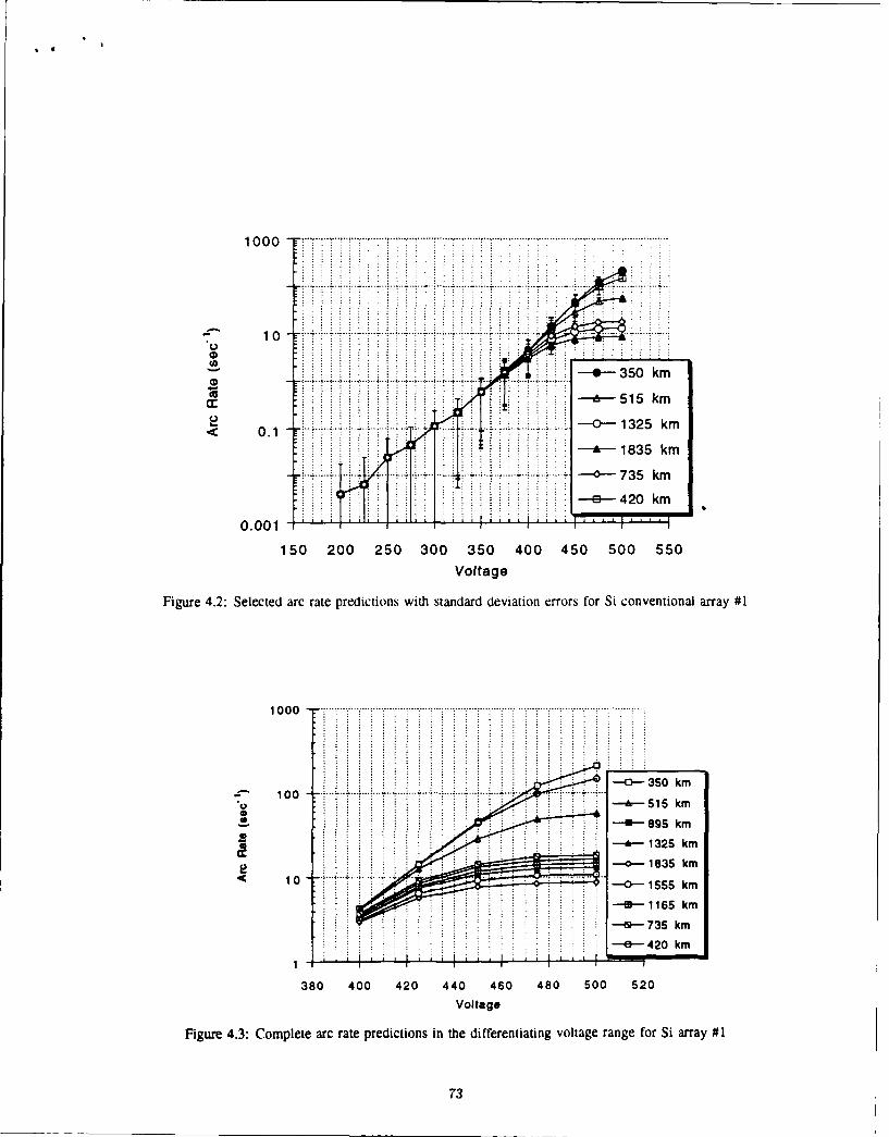
100
-0-350 km
cc - 515 km
--- 1835 km
.. ~ ~ .....-- 735 km
-e420 km
0.00 1
150 200 250 300 350 400 450 500 550Voltage
Figure 4.2: Selected arc rate predictions with standard deviation errors for Si conventional array #1
--0--350 km
o -'-515 kmo -6-895 km
-4132S km
H-o--1836 km
10~~ -O--55 km
M -1165 km
-t9-735 km
-e-420 km
380 400 420 440 460 480 500 520
Voltage
Figure 4.3: Complete arc rate predictions in the differentiating voltage range for Si array #1
73
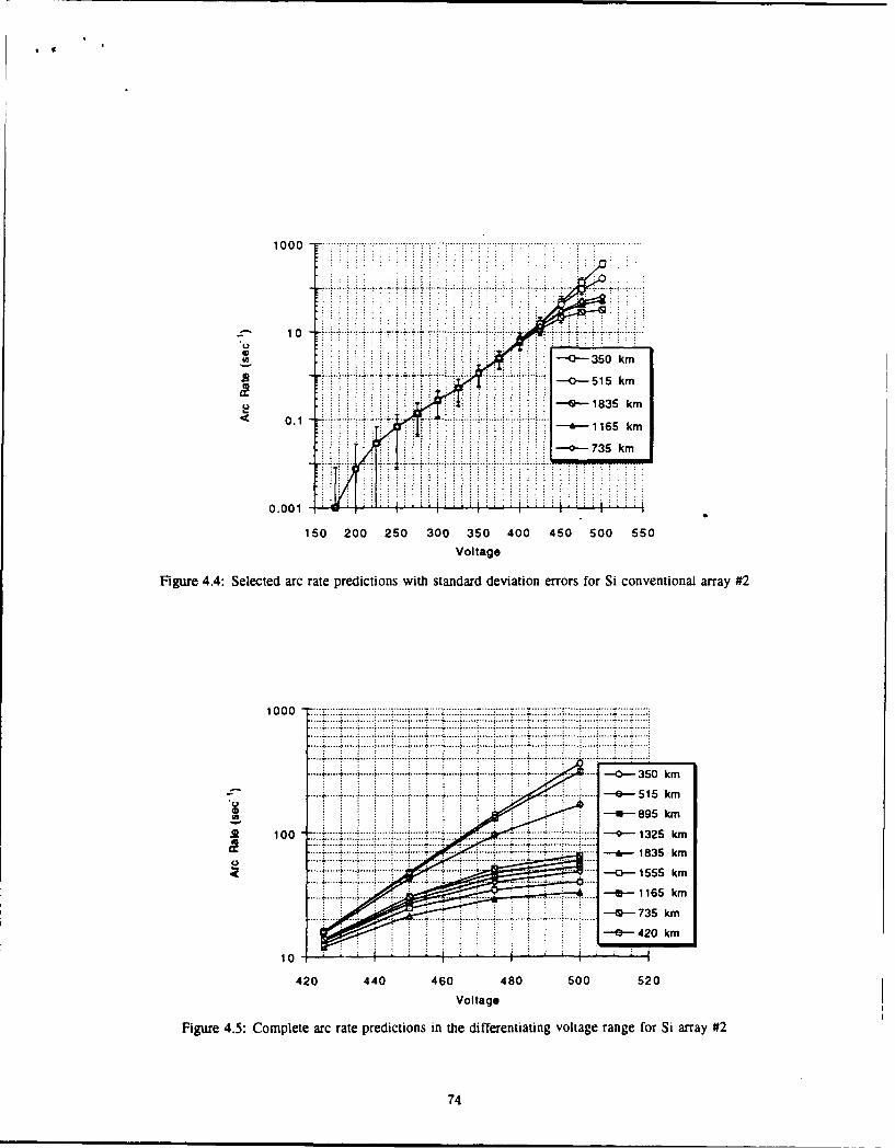
10 0 0 .............. .. ....
- 10 ......
..... ... 350 km
.. ...... 515 km
-s-1835 km< 0.1 -- 1165 km
-- 735 km
0.001
150 200 250 300 350 400 450 500 550Voltage
Figure 4.4: Selected arc rate predictions with standard deviation errors for Si conventional array #2
S......¶... .......... .......... *....... .
.... ... .... .... ...--. 350 km.....- e-515 km
o -0-895 km8 100 ......... 1325 km
...... ........- 1835 km
.......... ..- 0..- 1555 km
-Q-735 km-- 420 km
420 440 460 Vlae480 500 520
Figure 4.5: Complete arc rate predictions in the differentiating voltage range for Si array #2
74
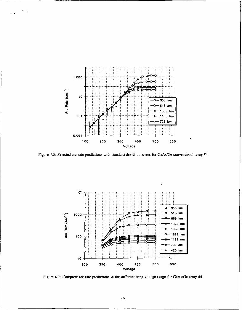
10 0 0 ......... .... .
0-0-515 km
-9-1835 km
-O-73S km
0.001
100 200 300 400 500 600Voltage
Figure 4.6: Selected arc rate predictions with standard deviation errors for GaAs/Ge conventional array #4
10 ..................................... ..........
--0- 350 km
1000U -- w-895 km
~1325 km-0- 1835 km
2 -0---1555 km.( 100 = . ..i.. .. -- 4..i.
* . -Ua 1165 km
-Q-735 km
-- 420 km
10
300 350 400 450 500 550Vol tag.
Figure 4.7: Complete arc rate predictions in the differentiating voltage range for GaAs/Ge array #4
75

1000.........
Cr -0-515 km
0.1 -8-1835 km-- 1165 km
..............420 km
0.001 ------ " -
100 200 300 400 500 600
Vol tag.
Figure 4.8: Selected arc rate predictions with standard deviation errors for GaAs/Ge conventional array #6
1000 ...................... ....... .......... . .......
S~..............,
-0---350 km
515Si km
o -4-895 km
--1325 km
-~1835 km
-40--1555 kmr'":-0-1165 km
-6--735 km
&-420 km
10
300 350 400 450 500 550Voltage
Figure 4.9: Complete arc rate predictions in the differentiating voltage range for GaAs/Ge array #6
76
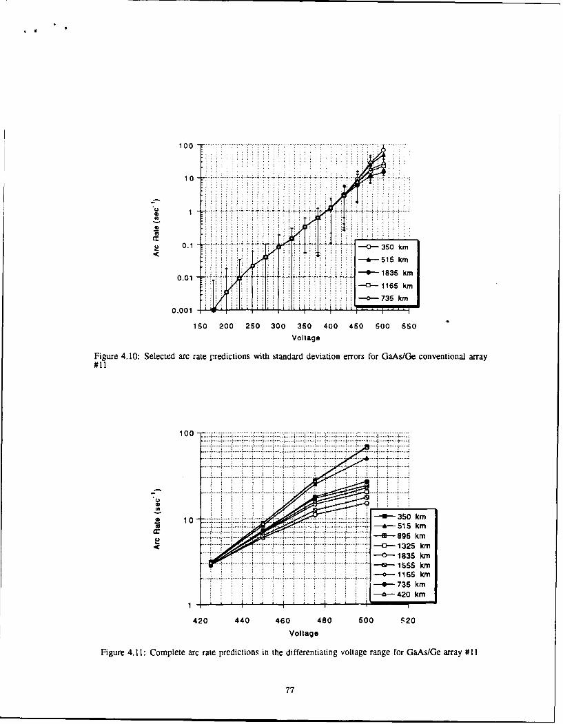
1 0 0.......... ...
1 0 .. ....- -------
u 0.1 --0-350 km-*515 km
...... 1835 km0.01
-0-)--1165 km-o- 735 km
0.001
150 200 250 300 350 400 450 500 550Voltage
Figure 4.10: Selected arc rate predictions with standard deviation errors for GaAs/Ge conventional array#11
100.............................
* 100-
.. .............. ... .. ..... .. .. . ..
420.............. 440......... 460 4. 500.52Vol.... tage ..
Figure~~~~~~~~~~~~~~~~~...... 4.11 Copeeacrt.r.ito.i.h ifrntaigvlaerne o asG ra 1
........ .....77 .

100
VU 1 -- 350 km
cc -~ 515 km
2 -- 0-895 kmS 0.1 --. --.
-- 1835 km-0-- 1555 km
-~-420 km
0.00 1
0 100 200 300 400 500 600Voltage
Figure 4.12: Selected arc rate predictions with standard deviation errors for APSA (#36)
1000. .. ......... .. .. . ... ..... ..... ,......1....
S:. :............ ........
100Q 355k
~ 10 -- 1835 km
-- 1165 km
-735 km
.... .... .... .... .... - 0- 420 km
200 250 300 350 400 450 500 550Voltage
Figure 4.13: Complete arc rate predictions in the differentiating voltage range for APSA (#36)
78

4.2 SAMPIE
The Solar Array Module Plasma Interactions Experiment (SAMPLE) is designed to pro-
vide NASA with data on the interaction of high voltage space power systems with the
ambient plasma environment of low earth orbit (LEO). The experiment will focus onthe investigation of the arcing and current collection of typical materials and geometries
likely to be a part of future high voltage power systems in LEO. The objectives SAMPLE
is intended to accomplish, fully described in its Technical Requirements Document [12],
are the following:
(1) characterize arcing on selected solar cell technologies by determining the magnitude
of the arc currents, the arc rates, and the arcing thresholds;(2) measure the collected plasma current versus the applied bias of these solar cell
arrays;
(3) test a pre-determined arc mitigation strategy for a selected solar cell design;
(4) measure the current collection on simple metal/insulator geometries;
(5) determine the dependence of arcing characteristics on the metal of the
interconnector;
(6) time permitting, study basic phenomena related to arcing and its effects such as
arcing from pinholes in coated conductors, arcing from anodized aluminum typical of
alloys and anodization processes being considered for large space structures, and
sputtering and degradation of metals biased at high negative potentials;
(7) characterize the space environment for use in data reduction and analysis; and(8) validate computer models.
4.2.1 Experiment Description
SAMPLE is to be carried on a shuttle flight currently scheduled for launch in early 1994.
The layout of SAMPLE is shown in Figs. 4.15 [13]. This metal box will mount on one
of the four top mounting positions of a Hitchhiker-M carrier, which is located in the
shuttle bay. Most of the instruments are located inside the box. These include the elec-
tronics necessary for experiment control and data storage, a pressure gauge to measure
background pressure, a langmuir probe to monitor plasma density and temperature, and
a V-body probe to monitor the shuttle potential with respect to the ambient environment.
The latter probe is crucial for determining the bias voltage since the power supply can
only apply voltage with respect to the shuttle ground, which will shift during SAMPLE
operations. In addition, the bias voltage needs to be with respect to the ambient en-
79

0Si (20 cells)---- Si (60 cells)---'O: ASEC GaAs/Ge (12 cells)
9ASEC GaAs/Ge (20 cells)"1 Spectrolab GaAs/Ge
APSA
0 0 0 . . . . . . . . . .
10 10 20 30 40 50 60
Voltage
Figure 4.14: Arc rate prediction comparison for all PASP Plus conventional arrays at 350km
vironment so the actual voltages applied need only be determined with the data of the
shuttle potential. This problem was accounted for in mission planning through extensive
modelling, and it is expected that the offset of the ground will be in the range of 10 to
25V. A sun sensor to measure the incidence angle is located on top of the box along with
the test modules.
A more detailed schematic of the positioning of the test modules on the experiment
plate is shown in Fig. 4.16. Three solar cell designs have been chosen to accomplish
objectives (1) and (2): the silicon conventional cells, a Space Station Freedom cell,
and the Advanced Photovoltaic Solar Array (APSA). Two of the modified Space Station
Freedom cells will test arc mitigation strategies to meet objective (3). The first will
test the effect of creating an overhang of the coverglass over the 8mil silicon cell. The
four exposed cell edges will have overhangs of 0, 4, 7. and 1 Ilmil respectively. The
second modified SSF cell will have its excess adhesive removed in a special treating
process to test the theory [101 that the arc discharge is actually a breakdown in water
vapor desorbed from the adhesive. The third SSF cell will test the computer prediction
that current collection is linear with exposed cell area. Multiple breakdown tests are
designed to determine the effects on arcing due to the metal material. The five metals
chosen are gold, silver, copper, aluminum, and tungsten. The first test consists of strips
80

Figure 4.15: SAMPLE experiment package
of Kapton Imil thick, 0.0625in wide, spaced 0.0625in apart on the metal. This simple
metal/insulator configuration is typical of many space power applications including the
solar cell/interconnector geometry. However, affixing the Kapton to the metal requires
the use of an adhesive bond, which complicates the arc process. The second test was
therefore designed to eliminate the dielectrics from the charging process. For these tests,
a stainless steel rod of 1mm diameter is suspended 1mm above the metal surface. These
rods are grounded, acting as anodes. Both tests are included as the first test is a better
model of real space systems while the second test isolates the metal's effect on the
arcing process. The three final experiments combine to fulfill objective (6). The first
is included on the multiple breakdown coupon, though it is not designed to test arcing.
This aluminum sample is coated with Z93, a thermal coating often applied to spacecraft
which has been found to collect electrons when biased positively under some conditions.
The second is the single breakdown test which will test a sample of anodized aluminum,
currently planned for the SSF main structure, for dielectric breakdown and arcing at high
voltage biases. The third is the snapover and current collection test. This includes 6
copper disks of lcm diameter covered with Kapton 3mil thick. A pinhole is centered in
the Kapton of each disk with hole sizes of 1-30mil.
The tests relevant to this research involve those concerning the actual solar cells:
silicon conventional, SSE and APSA. The silicon cells are 2cmx2cm, but otherwise are
81

-l 16" ---un Sensor
Snapover MO 0Experiment
SpaceS t a t io n
Si n gl eCell
Breakdown
N •- -- Breakdown0 OO0O0O1 Test
Silicon -I000-00 Multipl-Conventional 01500130Array 0 10000
100000~ Modified
Space Station
Figure 4.16: SAMPIE experiment plate layout
82

assumed to have the same characteristics as the PASP Plus cells in arrays #0-2. These
cells are planned to be used for 3 different tests, only one of which involves arcing. In
this test, only the four innermost cells will be used. The SSF cell is again 8cmx8cm,
and the APSA includes twelve 2cm x4cm cells. The material properties of these cells are
described in Section 4.1.1 and tabulated in Table 4.1.
The entire space experiment is expected to be completed during 12 hours facing the
ram velocity and 6 hours facing the wake. Each sample will be biased individually while
all others are held at the ground potential. The power supply will bias the solar cell
samples from 0 to -600V for the arcing tests. The bias trme varies significantly with the
voltage since the arc rate is known to increase substantially as the bias voltage becomes
more negative. The experiment times are expected to be the following: 40rain (2400sec)
at -120V; 20min (1200sec) at -150V; 5min (300sec) at -180V; 2min (120sec) at -210V,
60sec at -240V, -270V and -300V; 30sec at -400V; 5sec at -500V; and 2sec at -60OV.
4.2.2 Predictions
Arc rate predictions for SAMPLE are determined in the same manner as for the PASP
Plus predictions. The analytical model discussed in Section 2.1.2 is again used for the
conventional cell arrays, and the IRI model also is used to determine the ionospheric
conditions necessary for the analytical model. The shuttle orbit is assumed to be circular
with an altitude of 250km and an inclination of 28.50.
The arc rate predictions for the silicon conventional array and APSA are shown in
Fig. 4.17. Arcing is not predicted until the 210V step for the silicon array, but the thin
APSA is expected to experience arcing at 120V. These arc rate curves have the general
characteristics of the two dominating regions of 7-.,, and ro; however, the curves are
not as smooth due to the irregularity of the voltage and time intervals. The arc rates
are also significantly lower at the higher voltages than those predicted for the PASPPlus experiment. This is mostly due to the much shorter experiment time of only a few
seconds compared to the 20sec experiment time of the PASP Plus tests. In addition, only
4 silicon cells are used for arc rate measurements in this experiment compared to the 20
and 60 cells of the PASP Plus silicon arrays.The arc rate predictions for the SSF cell is left for future work. These predictions can
be made from an analytical model developed from the results of the numerical model
presented in Section 2.2, with experimental results used for model verification.
83
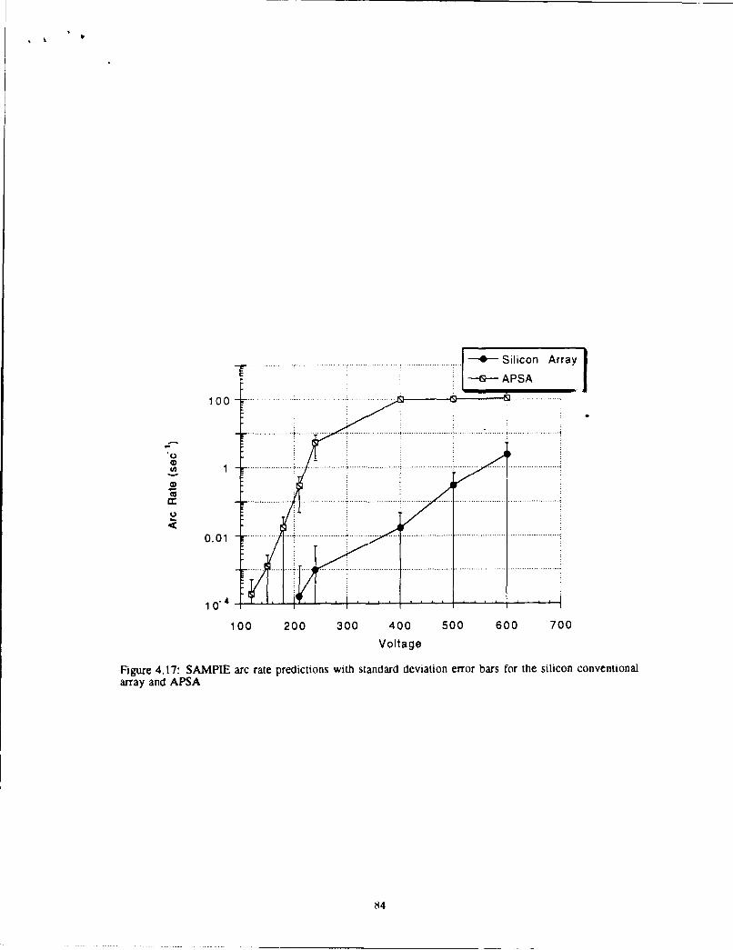
S. .......... .. ;...... ........ . . .......... ........ ....... ............... 0 S ilic o n A rra y
S• :. • APSA1
10
0 0 . ................. .. .. . ........ ... ... . ................ .......... . .. ... ... ... ....................
0.0
104 _
100 200 300 400 500 600 700
Voltage
Figure 4.17: SAMPLE arc rate predictions with standard deviation error bars for the silicon conventional
array and APSA
84

Chapter 5
Conclusions
The emergence of high voltage solar arrays has been driven by recent space system
designs which require high power levels. Consequ -tly, only recently has the negativeinteraction of arcing on high voltage solar arrays in low earth orbit been a concern. Since
arcing can eventually destroy solar cells, it is imperative to investigate methods to reduce
or even eliminate it as well as to develop methods to predict it for existing solar cells
which might be used on future high voltage solar arrays. This research has addressed
both of these needs.
5.1 Summary of Results
All of the research presented in this thesis has been based on the numerical and analytical
models discussed in Chapter 2. These models accounted for the ambient ion chargingand enhanced electron field emission (EFEE) charging processes which were previously
determined to be the two main factors leading to arc initiation. The numerical modelsimulates this arc initiation process by integrating the particle trajectories self-consistentlywith the dielectric surface charge. Electrons emitted from the conductor that hit the
dielectric surface released secondary electrons, creating a positive surface charge which
further enhances the electric field at the triple junction. With an EFEE charging site onthe conductor near the triple junction, the exponential dependence of the EFEE current
on the electric field causes the electric field to run away. This gives rise to arc initi,.tion.
The analytical model represents the time to arc initiation by the sum of the ambien, ion
charging time and the EFEE charging time. The numerical model was also modified
to represent the wrap-through-contact geometry using the same charging processes. The
electric field runaway, signifying arc initiation, occurs at the triple junction including
the semiconductor and the coverglass. Two different dielectric charging behaviors are
exhibited for relatively low and high field enhancement factors.
85

The models for conventional solar cells were used to determine methods of arcing
mitigation in Chapter 3. Based on the analytical model, five cell properties were varied
to determine their effect on the arc rate: the coverglass and adhesive dielectric thickness,
the interconnector work function, the secondary electron yield, the ratio of the dielectric
constants, and the length of the coverglass overhang above the interconnector. The
dielectric thickness was found to affect the arc rate, but significant reduction could only be
attained by large thicknesses which would be costly in mass addition. The interconnector
work function did not affect the arc rate much for typical metals, though very high
work functions decreased the arcing rates and very low work functions increased the
arcing rates at lower voltages. Secondary electron yields below unity eliminated arcing
since the electric field could not run away; yields just above unity, however, did not
reduce the arc rate significantly. Coverglass to adhesive dielectric constant ratios of
less than unity caused the surface charge near the triple junction to remain negative for
a considerably long time, thus significantly reducing the arcing rates. Overhanging the
coverglass above the interconnector also caused the dielectric surface to charge negatively
if the overhang was longer than the critical overhang. Overhangs less than the critical
overhang only acted as thicker dielectrics with no negative surface charging. Shorter
overhangs did not affect the arc rate much, but longer overhangs significantly reduced
arcing rates. Therefore, arcing rates can be best reduced by increasing the dielectric
thicknesses, selecting dielectric materials with coverglass to adhesive dielectric constant
ratios near unity, and overhanging the coverglass above the interconnector. Dielectric
secondary electron yields lower than unity will eliminate arcing at all voltage biases.
Arcing rates for actual solar cells were predicted in Chapter 4 for two near future space
experiments, Photovoltaic and Space Power Plus Diagnostics (PASP Plus) experiment and
the Solar Array Module Plasma Interactions Experiment (SAMPLE). Using the numerical
and analytical models, the high voltage biased conventional cell arrays were studied.
The most significant factors which discriminated the arcing rates in the EFEE charging-
dominated voltage range were the cell thickness and number of cells in the array. As
expected from the sensitivity scans, the cells with thinner dielectrics had higher arcing
rates at the low voltages. In addition, the increased number of EFEE emission sites due
to a higher number of cells increased the arcing rates.
86
S
5.2 Recommendations for Future Work
The numerical model for wrap-through-contact (WTC) cells should be involved in future
work. The model should be used to investigate the effects of different properties on the
EFEE charging time and to further study the two different charging behaviors seen. Amodified orbit integration scheme might be necessary to determine EFEE charging timeslonger than 10- 3 sec. To be successful, this may require a re-evaluation of the timestep
calculation. Also, an analytical model for WTC cells based on numerical and experi-
mental work would be very useful, particularly for future designs. With both numerical
and analytical models, mitigation strategies other than overhanging the coverglass could
be studied. When experimental data becomes available, the charging times and pro-cesses can be compared to determine any necessary modifications. The PASP Plus andSAMPLE missions should provide data for various types of WTC cells as well as forvarious coverglass overhang lengths for the Space Station Freedom cell.
For arc rate mitigation on conventional solar cells, experimental work should be done
to confirm the results of this research and to develop optimum cell designs for highvoltage solar array operation. This work should include tests of different coverglass
overhang lengths, which would confirm the critical overhang length hypothesis, and testsof different coverglass to adhesive dielectric constant ratios to determine the effects ofmaterial choice on the arc rate. In addition, doping procedures could be used to reduce thedielectric secondary electron yield below unity to test the hypothesis of no arc discharge
under these conditions. From these tests, a solar cell could be designed to optimize the
mass, efficiency, and arcing rate trade-off.
The arc rate predictions for the PASP Plus and SAMPLE will be useful in verifyingand possibly improving the numerical and analytical models. Since these experimentswill be launched in the next year or two, data will soon be available to compare with
the predictions presented in this thesis. Of particular interest should be whether themodifications used to account for the surface charge density variations were necessary
and whether the assumed value for 03o is always near 200. The latter is noted since inRef. [2] Cho indicated that this value was the only variable of freedom but it had to be
chosen in each case to match the slope of the arc rate curve in the lower voltage region.Additional research with the aid of the experimental results should be able to determine
these points.
87
Bibliography
[1] YA. L. Al'Pert. The Near-Earth and Interplanetary Plasma. Vol. 1, Cambridge
University Press, 1983, pp. 22-24.
[21 M. Cho, "Arcing on High Voltage Solar Arrays in Low Earth Orbit: Theory and
Computer Particle Simulation," Ph.D. Thesis, M.I.T., 1992.
[3] M. Cho and D. E. Hastings, "Dielectric Charging Processes and Arcing Rates of
High Voltage Solar Arrays", Journal of Spacecraft and Rockets, Vol. 28, pp. 698-706,
1991.
(41 Ferguson D. C., "The Voltage Threshold for Arcing for Solar Cells in LEO-Flightand Ground Test Results", NASA TM-87259, March 1986.
[5] H. Fujii, Y. Shibuya, T. Abe, K. Ijichi, R. Kasai, and K. Kuriki, "Laboratory Simula-
tion of Plasma Interaction with High Voltage Solar Arrays", Proceedings of the 15th
International Symposium on Space Technology Science, Kanagawa, Japan, 1986.
[6] N. T. Grier and N. John Stevens, "Plasma Interaction Experiment (PIX) Flight
Results", Spacecraft Charging Tecnology 1978, NASA CP-2071, pp. 295-314.
[7] N. T. Grier, "Plasma Interaction Experiment H: Laboratory and Flight Results",
Spacecraft Environment Interactions Technology Conference, 1983, NASA CP-
2359, pp. 333-348.
[8] 0. Hachenberg and W. Brauer, "Secondary Electron Emission from Solids", Ad-
vancement in Electronics and Electron Physics, Vol. 11, pp. 413-499, 1959.
[9] D. E. Hastings, M. Cho, and H. Kuninaka, "The Arcing Rate for a High Voltage Solar
Array: Theory, Experiments and Predictions", Journal of Spacecraft and Rockets,
Vol. 29, pp. 538-554, 1992.
[10] D. E. Hastings, G. Weyl and D. Kaufman, "The Threshold Voltage for Arcing
on Negatively Biased Solar Arrays", Journal of Spacecraft and Rockets, Vol. 27,
pp. 539-544, 1990.
88

[Il] B. G. Herron, J. R. Bayless and J. D. Worden, "High Voltage Solar Array Technol-ogy", Journal of Spacecraft and Rockets, Vol. 10, pp. 457, 1973.
[121 G. B. Hillard and D. C. Ferguson, "The Solar Array Module Plasma Interaction
Experiment: Technical Requirements Document", NASA TM-105660, 1992.
[131 G. B. Hillard and D. C. Ferguson, "The Solar Array Module Plasma Interactions
Experiment (SAMPLE): Science and Technology Objectives", to be published in the
Journal of Spacecraft and Rockets.
[141 R. W. Hockney and J. W. Eastwood. Computer Simulation Using Particles. McGraw-
Hill, USA, 1981.
[151 G. T. Inouye and R. C. Chaky, "Enhanced Electron Emission from Positive Dielec-
tric/Negative Metal Configurations on Spacecraft", IEEE Trans. Nuc. Sci., Vol. NS-
29, No. 6, December 1982, pp. 1589-1593.
[16] G. A. Jongeward, I. Katz, M. J. Mandell and D. E. Parks, "The Role of Unne'utralized
Surface Ions in Negative Potential Arcing", presented at the 1985 IEEE 22nd Annual
Conference, NSRE.
[17] R. V. Latham, High voltage Vacuum Insulation: The Physical Basis. Academic
Press, London, England, 1981.
[18] R. V. Latham, "Prebreakdown Electron Emission", IEEE Transactions on Electrical
Insulation, Vol. EI-18, June 1983.
[19] P. Leung, "Characterization of EMI Generated by the Discharge of a 'Volt' Solar
Array", Technical Report CR-176537, NASA, November 1985.
[20] "PASP Plus Experiment Specification," Phillips Laboratory, US Air Force, Jan 17,
1991.
[21] D. E. Parks, G. Jongeward, I. Katz and V. A. Davis, "Threshold-Determining Mech-
anisms for Discharges in High-Voltage Solar Arrays", Journal of Spacecraft and
Rockets, Vol. 24, pp. 367-371, 1987.
[22] D. B. Snyder, "Discharges on a Negatively Biased Solar Cell Array in a Charged
Particle Environment". Spacecraft Environment Interactions Technology Conference,
1983, NASA CP-2359, pp. 379-388.
[23] D. B. Snyder and E. Tyree, "The Effect of Plasma on Solar Cell Array Arc Charac-
teristics", Technical Report TM-86887, NASA, 1985.
89)
[24] N. J. Stevens, "Review of Interactions of Large Space Structures with the Envi-
ronment, Space Systems and their Interactions with Earth's Space Environment".
Progress in Aeronautics and Astronautics", Vol. 71, AIAA, Washington D. C.,
pp. 437-454, 1980.
[25] H. Thiemann and K. Bogus, "Anomalous Current Collection and Arcing of Solar-
Cell Modules in a Simulated High-Density Low-Earth-Orbit Plasma, ESA Journal,Vol. 10, pp. 43-57, 1986.
[26] H. Thieman, R. W. Schunk and K. Bogus, "Where do negatively biased solar arrays
arc?", Journal of Spacecraft and Rockets, Vol. 27, pp. 563-565, 1990.
90