AD-A263 277 - Defense Technical Information Center · AD-A263 277 a I NI D&sn w NEUTRON RADIATION...
40
AD-A263 277 a I NI D&sn w NEUTRON RADIATION INDUCED DEGRADATION OF DIODE CHARACTERISTICS (U) by S.M. Khanna, G.T. Pepper and R.E. Stone i2 E DEFENCE RESEARCH ESTABLISHMENT OTTAWA REPORT NO. 1155 93-08566 31 856 December 1992 Canadg IIIIIIIIIII BIMIIII Ottawa ~TN SA.IT ' Afil)l, 0~IQQ 26
Transcript of AD-A263 277 - Defense Technical Information Center · AD-A263 277 a I NI D&sn w NEUTRON RADIATION...
AD-A263 277 a
I NI D&sn w
NEUTRON RADIATION INDUCED DEGRADATIONOF DIODE CHARACTERISTICS (U)
by
S.M. Khanna, G.T. Pepper and R.E. Stone
i2 E
DEFENCE RESEARCH ESTABLISHMENT OTTAWAREPORT NO. 1155
93-0856631 856 December 1992Canadg IIIIIIIIIII BIMIIII Ottawa
~TN SA.IT
' Afil)l, 0~IQQ 26

NEUTRON RADIATION INDUCED DEGRADATIONOF DIODE CHARACTERISTICS (U)
by
S.M. Khanna, G.T. Pepper and R.E. StoneRadiation Effects Section
Electronics Divisiona
DEFENCE RESEARCH ESTABLISHMENT OTTAWAREPORT NO. 1155
PCN December 1992041LS Ottawa

ABSTRACT
Neutron radiation effects on diode current-voltage characteristics have been studied
for a variety of diodes over IxlO'3 to 3x10 5 n/cm2 I MeV equivalent neutron fluence range.
A classification scheme consisting of three types of neutron effects on diode forward
characteristics is proposed here for the first time. For constant forward current lF higher than
that in the generation-recombination regime, the diode voltage VF either increases with
fluence 4P (Type 1 diode), or VF first decreases with 4) at lower fluence levels and then
increases with 4) at higher fluence levels (Type 2 diode), or VF decreases with 4) at all fluence
levels used in this work (Type 3 diode). Most of the previous results on p-n junction diodes
correspond to Type I diode results. Type 2 diode results are rather rare in the literature.
Several examples of Type 2 diode results are presented here. Type 3 diode results are
reported here for other types of diodes not reported earlier. These results are explained
qualitatively in terms of the theories for a p-n junction and for radiation effects on
semiconductors. It is shown here that a Type 3 diode could be developed as a high neutron
fluence monitor with three orders of magnitude higher upper limit than the Harshaw p-i-n
diode neutron fluence monitor under evaluation at the US Army Aberdeen Proving Grounds,
Aberdeen, Md. The results also suggest a methodology for radiation hard diode
development.AcccFion ror
NiTS (Js \C!IDTiC (I : ..
U 2
!t Ey.. ...... ..
N ------
1A,_

RiESUMNI
Les effects de radiation de neutrons sur la carract~ristique courant-voltage de
diodes ont Wt~s 6tudi~s pour une varidtd de diodes sur une gamme neutron-fluance
dquivalente de Ix IO01 . 3xA0R5 n/cm2 1 MeV. Une astuce de classification consistant de
trois types d'effets de neutron sur la carract~ristique avant de diodes est proposde ici pour
la premiere fois. Pour un courant avant constant IF plus 6lev6 que celui du rdgime
gdn6ration-recombination, le-voltage de diode VF ou alors augmente avec la fluance 4,
(diode du type 1), ou alors VF diminue pour commencer avec ,D sous faible niveau de
fluance pour ensuite augmenter avec 4, sous plus fort niveau de fluance (diode du type 2),
ou alors VF diminue avec 4) sous tout niveau de fluance utilis6 dans ce travail (diode du
type 3). La plupart des r6sultats anterieurs sur les diodes A jonction p-n correspondent aux
r~sultats des diodes du type 1. Les diodes du type 2 sont plut6t rares dans la littdrature.
Plusieurs exemples de diodes du type 2 sont prdsentds ici. Les r~sultats des diodes du type
3 sont observes ici pour d'autres types de diodes non reportds plus t6t. Ces rt~sultats sont
expliqu~s qualitativement-en termes des th6ories pour une jonction p-n et pour les effects
de radiations sur semiconducteurs. II est pr6dit qu'une diode du type 3 pourrait &re
d~velopp6e comme monitrice de haute fluance de neutron avec une limite sup~rieure de
trois ordes de grandeur plus dlev6e que la diode p-i-n monitrice de fluance de neutron sous
Evaluation IT'US Army Aberdeen Proving Grounds, Aberdeen, Md. Les r6sultats
sugg~rent aussi une mdthodologie de d~veloppement de diode i l'6preuve des radiations.
bv

EXECUTIVE SUMMARY
Neutron radiation effects on the current-voltage (I-V) characteristics for a variety
of diodes have been studied over lxIO0I to 3x10' 5 n/cm 2 I MeV equivalent neutron fluence
range. A classification scheme consisting of three types of neutron radiation effects on
diodes is suggested here for the first time. These results and all prior similar results can
be grouped into three categories corresponding to Type 1, Type 2,and Type 3 diodes as
defined later in this work.
Most of the earlier results for neutron radiation effects on diodes correspond to
Type 1 diodes. Type 2 diode results are rather novel in character. There have been only
few reports on such effects on diodes in the literature. Type 3 diode results are observed
here for other types of diodes not reported earlier. These results can be explained
qualitatively on the basis of the existing theories for a p-n junction and for radiation
effects on semiconductors.
Applications of these results with vastly improved performance in two areas is
predicted. These results show that a Type 3 diode could be used for high neutron fluence
measurements. This monitor has at least three orders of magnitude higher upper limit for
neutron fluence measurement than the Harshaw p-i-n diode neutron fluence monitor which
is under evaluation at the US Army Aberdeen Proving Grounds, Aberdeen, Md.
Further, the results also suggest the possibility of developing a radiation hard diode.
vii

TABLE OF CONTENTS
ABSTRACT .............................................. iii
RI• SUM .. ............................................... v
EXECUTIVE SUMMARY .................................... vii
1.0 INTRODUCTION ....................................... 1
2.0 EXPERIMENTAL MEASUREMENTS .......................... 4
3.0 EXPERIMENTAL RESULTS ............................... 53.1 PRIOR RESULTS ................................. 53.2 PRESENT WORK: FORWARD I-V CHARACTERISTICS ........ 53.3 REVERSE I-V CHARACTERISTICS .................... 17
4.0 DISCUSSIONS ........................................ 20
5.0 APPLICATIONS ....................................... 25
6.0 CONCLUSIONS ........................................ 26
7.0 ACKNOWLEDGEMENTS ................................. 28
8.0 REFERENCES ......................................... 29
APPEND IX ............................................. 31
ix

LIST OF FIGURES
Fig. 1 Typical I-V characteristics (Fig. la) and percentage change inforward voltage and reverse current (Fig lb) of diodes before andafter neutron irradiation from the published data (".2) ........ ............... 6
Fig. 2 Forward log I-V characteristics of (a) IN 914 and (b) IN 4006diodes before and after neutron irradiation ....................... 7
Fig. 3 Forward log I-V characteristics of (a) MVAM 109 and (b) MPN3401 diodes before and after neutron irradiation ................... 8
Fig. 4 Forward I-V characteristics of Type 1 diodes before and afterneutron irradiation .................................... 9
Fig. 5 Forward I-V characteristics of Type 2 diodes before and afterneutron irradiation. . ........................... 11
Fig. 6a Forward I-V characteristics of Type 3 diodes before and afterneutron irradiation .................................... 13
Fig. 6b Forward I-V characteristics of Type 3 diodes before and afterneutron irradiation. .................................... 14
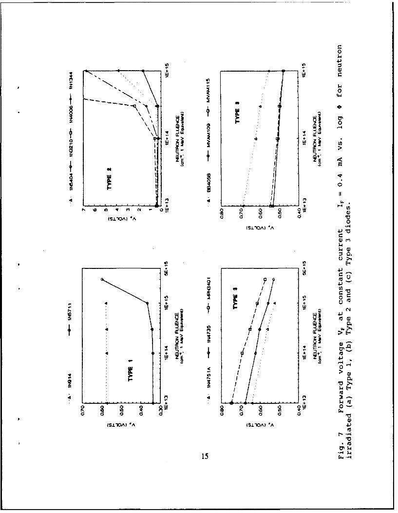
Fig. 7 Forward voltage VF vs. log (D at constant current IF = 0.4 mA forneutron irradiated (a) Type 1, (b) Type 2 and (3) Type 3 diodes ..... 15
Fig. 8 Change in forward voltage AVF at constant current IF = 0.4mA vs.log 4 for neutron irradiated (a) Type 1, (b) Type 2 and (c) Type 3diodes ... . . . . . . . . . . . . . . . . . . . . . . . . . . . . . . . . . . . . . . . . . 16
Fig. 9 Reverse I-V characteristics for (a) 1N4735A and (b) 1N4751 Zenerdiodes irradiated at different neutron fluence levels ................ .18
Fig. 10 Reverse current 'R at constant reverse voltage Vf vs. log 4I for(a) IN4735A and (b) 1N4751 Zener diodes ..................... 19
xi

1.0 INTRODUCTION
It is well known that nuclear radiation can destroy or substantially degrade the
performance of semiconducting electronic devices and systems. The permanent damage
can be estimated from an analysis of their pre and post irradiated electrical characteristics.
As a first step in understanding the radiation damage mechanisms in such devices, it was
decided to study the electrical characteristics of different variety of diodes including p-n
junction, p-i-n and Schottky diodes. Degradation of electrical parameters and eventual
total failure of such devices can begin at as low as (10"l-1012) n/cm2 1 MeV equivalent
fluence range. Such devices are amongst the simplest of all semiconducting device
structures and the corresponding results are therefore more amenable to analysis. An in-
depth investigation of nuclear radiation effects on these devices can also lead to a better
understanding of radiation effects in more complex semiconducting devices consisting of 2
or more p-n junctions.
In the present report, we give results on the effects of neutron irradiation on the
current-voltage (I-V) characteristics of twelve different types of commercial p-n, p-i-n and
Schottky diodes. It was observed that all of these results can be divided into three groups
which are described later on in this report.
Most of the published work on neutron radiation effects on I-V characteristics
of diodes could be classified into one group'"5'. The second type of results described here
are rare in the literature(3 ) and will be discussed in some detail. The third type of results
have been reported previously for a select type of diodes, i.e. p-i-n diodes, only"). This
type of results have been observed in this work for other types of diodes also.
Preliminary results on neutron radiatiorn effects on different diodes studied in this report
were presented earlier by one of the authors I. This work has led to an in-depth
radiation damage study due to different types of radiations for a specific diode, viz. MRD
500 p-i-n diode made by Motorola Co. These results are being reported separately in a
companion DREO Report(8) .

There have been several investigations on nuclear radiation damage in p-n and
p-i-n diodes('--'. This is mainly due to their application in a variety of electronic devices
in different frequency regimes and their use as a radiation monitoring sensor. Recently,
there has been a renewed interest in this field due to their application in electro-optical
systems and in high energy physics experiments in new high energy high intensity
eolliders -u
Radiation damage in a semiconducting device occurs mainly due to Ionization
and displacement damage in semiconducting materials and oxide barrier regions of the
device (").3 In the present paper, we will be concerned with radiation effects due to
displacement damage only. Briefly, the interaction between nuclear radiation and
semiconductor lattice could lead to different types of defects in the lattice structure. The
defect could be simple, such as a Frenkel defect, or be a complex defect pair, such as a
vacancy-vacancy pair or a variety of possible complexes between the vacancy, impurity
atom and host lattice. These defects lead to localized impurity levels within the energy
gap of the host semiconductor. The energy and other characteristics of these levels could
vary to a great extent. Thus, both shallow and deep levels with different charge states are
observed although deep defect states are more common. The characteristics of these states
affect the electrical properties of the semiconductor material and hence, the
semiconducting device under study.
.The major and most common source of degradation of diode characteristics on
neutron irradiation is due to the degradation of minority carrier lifetime. Reduction in
minority carrder lifetime due to irradiation could lead to a reduction in conductivity
modulation effect in the high current regime, Another source of device degradation is the
reduction of base conductivity on irradiation. In addition, in the generation- recombination
region, there will also be excess forward current due to additional recombination centers
created by neutron radiation. The latter effect could be ignored if one is working well
outside this regime. The relative contributions from these different phenomena depend
upon the current level, and device electrical and physical parameters. Further, the
2

relative significance of these effects could change with irradiation. As a result, a diverse
variety of neutron radiation effects on diodes, as observed in the present work, are
possible.
Section 2 gives the details of experimental procedures and some specifications
of the samples used in this work. Sections 3 and 4 give the results of experimental
measurements and their discussions respectively. Possible applications and main
conclusions are summarized in Sections 5 and 6 respectively.
3

2.0 EXPERIMENTAL MEASUREMENTS
Appendix A gives some of the pertinent specifications of the different types of
diodes studied in this work. These diode: provide a representative sample of diodes
currently in commercial use. The I-V characteristics of the diodes were measured with a
Hewlett-Packard HP 4145B semiconductor parameter analyzer operated under the control
of an IBM-PC through an HP-IB interface. All measurements were taken at =250C.
In the present work, typical I-V characteristics for an unirradiated diode
represent an average of I-V characteristics of six diodes of the same type. Typical
forward and reverse I-V characteristics for unirradiated diodes were determined for all
twelve different types of diodes used in this work. These measurements also assisted to
some extent in defining the range of I-V measurements that can be carried out without
thermally annealing the irradiated diodes.
The diodes were neutron irradiated at the US Army Pulse Radiation Facility
(APRF), Aberdeen Proving Grounds, Aberdeen, MD. All devices were irradiated with
junctions shorted to avoid damage due to radiation-induced ,Thotocurrents and static
charges. Five separate batches of diodes were prepared with each batch containing the
twelve types of diodes. These batches of diodes were irradiated with 1 MeV neutron
fluence of lx1013, lx1014, 3x10 14, Wx1011, 3xl0's n/cm2 .
The I-V characteristics of neutron irradiated diodes were measured
approximately one month after their removal from the reactor. This delay was required to
allow neutron activation products to decay sufficiently to permit their safe handling. Each
I-V characteristic of an irradiated diode in this report represents an average of
measurements taken for several (two to four) devices of the same kind. The temperature
of the devices was maintained at --25°C during neutron irradiation. Device
characteristics were also measured at this temperature to minimize any annealing effects.
4

3.0 EXPERIMENTAL RESULTS
All of our results and the published results for the forward I-V characteristics
of neutron irradiated diodes could be divided into three groups. The corresponding diodes
are termed as Type 1, Type 2 and Type 3 diodes respectively. We limit our discussion to
the voltage region beyond the generation-recombination region in the diode forward
characteristics. Thus, the present results and discussion are applicable to the diffusion and
high current regimes in a diode.
3.1 PRIOR RESULTS
Typical previous results for neutron radiation effects on p-n junctions and some
p-i-n diodes are shown in Figs. la and lb ".-2). These results show that the rate of change
of current with voltage decreases with irradiation. Thus, an increase in the diode forward
voltage at constant current on neutron irradiation is reported in most previously published
results for neutron radiation effects on p-n junctions. At the same time, the reverse
leakage current increases and breakdown voltage becomes more negative with irradiation.
These results correspond to Type 1 diodes described below.
3.2 PRESENT WORK: FORWARD I-V CHARACTERISTICS
A wide range of neutron radiation effects on the I-V characteristics of diodes
were observed. Figures 2 and 3 show representative results for the I-V characteristics of
some of these diodes before and after irradiation with neuutons. These results can be
grouped into three categories as discussed below.
Type 1 Diode - Figure 4 shows pre- and post-irradiation forward I-V characteristics of
1N914 switching diode and 1N5711 Schottky diode. It is noted that the I-V characteristics
of the diodes in this group are shifted to higher voltages on irradiation. This corresponds
to an increase in the diode voltage at constant current on irradiation. Such diodes are
named as Type 1 diodes in this report. It should be pointed that most of the published
results on neutron radiation effects on p-n junctions (see Figs. la and lb) fall under this
category.

I
I
P~REWRATIOt4 PO8T-UMAADATION/
//
• V
(a)
100: 100
10 10
S. £
>--
0.1 0.110"1 1012 i0'O 1014
NEUTRON FLUENCE (cm ")
(b)
Fig. 1 Typical I-V characteristics (Fig. la) and percentagechange in forward voltage and reverse current (Fig 1b) of diodesbefore and after neutron irradiation from the published data "'b.
6

Neutron Fluence (cm-2, 1 MeV Equivalent):
0 1E 13 1E14 3E14 1E15
10-'
10-3
10-4
U 10"o
10".
S _ 1 0 "7
10-010-I0
0.00 0.10 0.20 0.30 0.40 0.50 0.60 0.70
IN914 DIOOE FORWARD VOLTAGE (V)
(a)
Neutron Fluence (cm-2 , 1 MeV Equivalent):
0 1E13 1E14 3E14 1E15
S10--2
1° -4 ...... ... . . . ._.. .
10- 4 /
_ 10
10-9'
10-,1o ,0 2 3 4 5
1N4006 DIODE FORWARD VOLTAGE M/)
(b)
Fig. 2 Forward log I-V characteristics of (a) 1N914 and (b)
1N4006 diodes before and after neutron irradiation.
7

Neutron Fluence (cm-2 1 MeV Equivalent):
0 1E13 1E14 3E14 1E15
10-I
10 14 • t
10-4
S..- > .-- -10-4 .
10-7
/10" -10-4'
1 0 -*t, I ,
10-11
0.00 0.20 0.40 0.60 0.80 1.00
MVAM 109 DIODE FORWARD VOLTAGE (V)
(a)
Neutron Fluence (cm-2 . 1 MeV Equivalent):
0 1E13 1E14 3E14 1E15 3E15
I- 0-
10-4- - .
10---
10-' /4 " ' -
S1 0.0110-io - .
0.00 0.20 0.40 0.60 0.80 1.00
K1:N3401 DIODE FORWARD VOLTAGE (V)
(b)
Fig. 3 Forward log I-V characteristics of (a) MVAY109 and (b)MPN3401 diodes before and after neutron irradiaticn.
8

Neutron Fluence (cm" 2. 1 MeV Equivalent):
0 1E13 1E14 3E14 1E15
0.20Z /0
0.15
AV /
0., 0
3:7IL 0.05
0.000.40 0.50 0.60 0.70
1N914 DIODE FORWARD VOLTAGE (V)
(a)
Neutron Fluence (Cm-2 , 1 MeV Equivalent):
0 1E13 1E14 3E14 1E15020
I. /'0.15-/
• I.
0.10 ,/
0.05
0.000.00 0.10 0.20 0.30 0.40 0.50 0.60 0.70
IN5711 FORWARD VOLTAGE (V)
(b)
Fig. 4 Forward I-V charanteristics of Type 1 diodes before andafter neutron irradiation.
9

Type 2 Diode - Next, we describe a different type of neutron radiation effect observed
for some of these diodes. Such effects on diodes are not commonly known and should be
carefully interpreted. Figure 5 gives the pre- and post-irradiated I-V characteristics for
1N1344, 1N3210, IN4006 and 1N5404 rectifier diodes. The I-V characteristics of the
diodes in this group are shifted to lower voltages on irradiation up to a certain radiation
level which varies with the diode. Above this level, the shift in I-V characteristic is
reversed. The I-V characteristic is now shifted back to higher voltages towards the I-V
characteristic for the unirradiated diode. At some higher fluence level which varies with
the diode, the I-V characteristic of the radiated diode is shifted towards higher voltages
even beyond the I-V characteristic for the unirradiated diode. Thus, in such diodes, the
forward voltage across the diode at constant current first decreases with radiation initially
up to a certain fluence level. Above this fluence level, the diode voltage at constant
current begins to increase with radiation and eventually becomes equal to that for the
unirradiated diode at that current level. Above this radiation level, the diode voltage
continues to increase with fluence.
Thus, on irradiation, the change in diode forward voltage at constant current, as
compared to its pre-irradiated value, AV = (V).d,.., -(V)i,,,,I,., is increasingly negative
with increasing neutron fluence up to a certain fluence level. Above this level, the
absolute change, I AV I , in diode forward voltage begins to decrease with fluence and
eventually becomes zero. On further increasing the fluence, the change in diode forward
voltage, AV, is positive and increases with fluence. The diodes with this type of radiation
response are termed as Type 2 diodes in this report. There have been few results in the
literature which correspond to Type 2 diodes 3.
Type 3 Diode - A third type of neutron radiation effect on the I-V characteristics of
some diodes used in this work is shown in Figs. 6a,6b which show pre- and post-
irradiation forward voltage I-V characteristics of MPN3401 switching diode, 4735A and
4751A Zener diodes, and BB405B, MVAM 109 and MVAM 115 varactor diodes. On
10

0
'-441
40
4-J
T o 0
%4J
04 01 1 ,
0 a
o i 0 0 2
(Z-3 (3-30Ita) JJJmuV (V)~0 lpdi- ±Nvm~iO .1PA%. 30
E-
11W~

irradiation, the I-V characteristic of this type of diode is shifted increasingly to lower
voltages for all levels of irradiation used in this work. The change in diode forward
voltage, AV, is always negative and I AV I increases with neutron fluence level. Diodes
with this type of radiation response are termed here as Type 3 diodes. As far as is known
to us, similar type of radiation response has been reported for p-i-n diodes only(56 ). In the
present work, we report this behaviour for other type of diodes also.
It is useful to examine the forward voltage VF at a fixed forward current IF vs.
log D for these diodes. Figures 7a, 7b, and 7c give VF vs log 4P at IF = 0.4 mA for
Type 1, Type 2, and Type 3 diodes respectively. Using this data, the change of forward
voltage z"VF at a constant IF = 0.4 mA is determined at different radiation levels. These
results are shown in Figures 8a, 8b, and 8c for Type 1, Type 2, and Type 3 diodes
respectively. It should be noted that the selected constant current level is arbitrary so long
as it is outside the generation-recombination region. The suggested classification of
radiation effects on diodes would be valid at some higher current level such as 2 mA also
as can be seen from Figs. 4-6.
For Type I diodes, there is a small, approximately linear increase in the change
in diode forward voltage, AVF, at a fixed current IF, with log 4, up to a certain fluence
level _ 10i4 n/cm 2 as shown in Figs. 7, 8 and 4. Beyond this level, AVF increases
sharply and non-linearly with log C. These results are similar to the previous results on
neutron radiation effects on diodes~'"," and will be discussed further in this report.
For Type 2 diodes (see Figs. 7, 8 and 5), AVF is negative and I AVF I
increases with log 4,. Beyond a certain fluence level, the increase in AVF I with
fluence reaches a maximum value. Above this fluence level, I AVF begins to decrease
with fluence although AVF still remains negative. The fluence, at which the radiation-
induced change in the I-V characteristic reverses its trend, varies with the diode and is
termed here as IR,. At some value of ,i > *R,, AVF becomes zero. At still higher
fluence levels, AVp becomes positive and increases non-linearly with fluence.
12

Neutron Fluence (cmr0. 1 MeV Ecquivalent):
0 1613 1E14 3E14 6I15 3EI50203 il i0.15
Ojosj0.1 • / -
0.00 :~/ ,
,, /7 /
0.40 O.,0 0. -0 0.70 O.8O 0.90
mPN3401 DKX0E FoARwAD vcTA.E m
Neutron Fluenre (c•"2, 1 MeV Equivalent):O 1613 1614 3614 1615 31615
oao , I "
0.120 ,~5 ~S/ I I
I. . I•I 0.10 1 ,
* ,'"/
WO-
0.000.30 0,40 0.50 0.60 0,70 O.8O
1N4736A 0OOCE FCRWAPO V40TAGE M
Neutron Fluence (cmn-. 1 MeV EQuivalent):
0 1E13 -E14 1E15020
S1 I
0•15 1
0,00 . . . . """-" " • . .O.20 0.30 00 0.50 080 0.0 OO Ot
Fig. 6a Forward I-V characteristics of Type 3 diodes before andafter neutron irradiation.
13

Neutron Fluence (crnm'. 1 MeV Equivalent):
(5 ;E 3 -E 1-4 3E 14 3 1-5
020 *
0.6/ :
0.10 -/ /41."10
IL 0,/ I / -,/
0.30 0.40 0W 0.60 0.70 0.80
S46 DOOME FORAMD VOLTAGE M
Neutron Fluence (cm'. 1 MeV Equivalent):
0 1E13 1E14 3E14 1E15020 '
0.16 if 1' ,,
M.10 Ii
0.000§20 030 0.j: 0 0 oJ00 0.70
MV016I09 011 FC II) VOLTAGE M
Neutron Fluierce (cm-t, 1 MeV Eqluivalent):
0 1E13 1E 14 3E14 1E 15
020
020 0.20 0.40 0.5 0W 0.70 0.0
oAMI IS 010M PWAM VCLTA4 M
Fig. 6b Forward I-V characteristics of Type 3 diodes before andafter neutron irradiation.
14
o0
÷ .w
< 0
. I I I
4E-4
4. 4J
o o
(SJ.•OAV A (0J0 0A 0A 0,
4 0
P•.w -
. . . .. . 4 L 4
0 0
(S±LIA) 'A (S.LIOA? *A 4
15 - **

0
4.)
+ 4
/ /
0
-~E-4
1:1
E4.
uu.
0>
/ 07
w w44
161

Fo, Type 3 diodes, AVF remains negative at all fluence levels used in this work
and varies - linearly wihh log 4, up to the highest fluence level (- 3x1O0• n/cm2) used
here (see Figs. 7, 8 and 6).
3.3 REVERSE I-V CHARACTERISTICS
Reverse I-V characteristic measurements were limited to Zener diodes only.
Figures 9a and 9b give log IR vs. VR for 1N4751A and 1N4735A Zener diodes
respectively at different levels of neutron irradiation. The reverse current 'R at a fixed
reverse voltage VR increases with neutron fluence. Figures 10a and 10b give log IR vs.
log 4, at three values of reverse voltage VR for these Zener diodes. This data shows that
'R increases by about 2 to 3 orders of magnitude in both types of Zener diodes. Further,
the Zener voltage Vz changes to more negative voltages with neutron fluence. At 3x10¹⁵
n/cm2, the absolute increase in I AVz I is - 100 mV for 1N4735A (Vz - 6.2 V) and is
, 2 V for 1N4751A (Vz - 30 V) Zener diodes. These results for the increase in
reverse current and absolute value of Zener breakdown voltage confirm the trend of
neutron radiation effects observed in other Zener diodes"'2 ). The radiation-induced
changes in the reverse electrical characteristics of Zener diodes could be important and
should be taken into account in circuit design.
17

-2 ?AAT
VM fkADATEO
ý5 -4
- -6 -- -- E14
-10 -
-120 1 2 3 4 5 6 7
V. (V)
(a) 1N4735A
-2
4 II LtAPADIA1ED- 4
C~ -6 1E14
* 3E14
leis... _..• .• .-• ..- J . .. : - ,1
-12
0 10 20 30 40
V (V)
(b) 1N4751
Fig. 9 Reverse I-V characteristics for (a) 1N4735A and (b)1N4751 Zener diodes irradiated at different neutron fluence levels.
18

-5
0
"A -7 1 4 VOLT
8-8 0 3 VOLTS
_1 _g o5 VOLTS
-10
-1112.50 13.50 14.50 15.50 16.50
LOG ((0) (cm-2 )
(a) 1N4735A
-5
$ -6
-7 A 5 VOLTS
0 15 VOLTS
0 25 VOLTS
-10
-1112.50 13.50 14.50 15.50 16.50
LOG (0) (cm")
(b) 1N4751
Fig. 10 Reverse current IR at constant reverse voltage VR vs.log 4 for (a) 1N4735A and (b) IN4751 Zener diodes.
19

4.0 DISCUSSIONS
All of the results described in Section 3 can be explained qualitatively in terms
of radiation damage to the junction and base region of the diode. Quantitative analysis of
the data is not possible at present due to a lack of data for the electrical and physical
parameters of the devices used in this work. Various physical phenomena which affect
the diode characteristics on irradiation have been pointed out earlier in Sec. 1.
The applied voltage VA across the diode is given by
v= vf + VJ
- I ( Rn + RP ) ÷VJ (1)
where V8 represents the sum of ohmic voltage drops IR, and IRK, across the neutral n and
p regions of the diode respectively and V, is the change in voltage across the junction due
to an applied voltage VA across the diode. In the case of a p-i-n diode, VB would
correspond to the voltage drop across the intrinsic (i) region. Normally VB is small and
can be ignored at low currents. However, both components of rhs of Eq. (1) should be
taken into account for comparing the I-V characteristics of a diode before and after
irradiation.
The change in V, on neutron irradiation is thus the sum of changes in V, and
VB. It will be shown in the following that (dV1/d,), is always negative and (dV,/d4,), is
always positive. The magnitudes of these two components depend on device dimensions
and electrical properties of the materials making up the device. Thus, the change in VA
with fluence, (dVA/d,)I, could be negative, positive or zero depending on the values of
these respective components. The feasibility of (dVA/d)l, being equal to zero, at least in
theory, is particularly attractive for developing rad-hard p-n junctions and p-i-n diodes.
20

The current through an ideal diode in the diffusion current regime is given by
the Shockley equation:
ffVa
I e ( - - ( 2 )
where Is is the saturation current, I is the diode current, q is the electronic charge, k is
Boltzmann constant and T is the device temperature. The saturation current Is is given by
,, Aqni LI.VNA LpND(3I, = A 2n• D, + _D
where ND and NA are the donor and acceptor densities, L. and LP are the diffusion
lengths, D. and DP are the diffusion coefficients, ni is the intrinsic carrier density and A is
the cross-sectional area of the diode. For simplicity, let us consider an abrupt junction
with say ND > > NA. This leads to
qVjAqn2 Dn ( e k- _. ) (4)I Aqni L nNA
Further,
Ln = Vf'-nr n
where r. is the carrier life time. Substituting this in Eq. (4) and for V, > > kT/q
Aqz21 , '
vrvnNA
21

or Vj - (in (N (6)
q Aqnif2
Substituting Eq.(6) in Eq.(1), we have
VA = I ( RP + R, + k in INAV,, (7)
q AqnJ2 VI
Thus, the change in I-V characteristics of a diode on neutron irradiation is the
sum of two components corresponding to the changes in each of the two rhs terms in Eq.
(7). Neutron irradiation could lead to poor conductivity modulation and decrease in base
conductivity which would result in an increase in V.. On the other hand, the life time 70
of the carriers decreases with neutron irradiation which leads to a decrease in the junction
voltage. Thus neutron irradiation would always lead to a positive value for the change in
the first rhs term in Eq. (7) and a negative value for the change in its second term.
Results for Type 1 diodes could be explained on the assumption that on
irradiation, the change in the ohmic term in Eq.(7) corresponding to the conductivity
change in the base or i region of the diode dominate the change in the voltage drop across
the junction region. This would lead to an increase in the applied voltage across the diode
at constant current with neutron irradiation as has been observed for Type I diodes in the
present work (see Figs. 4, 7, and 8) and in other published diode results ("I (see Fig. 1).
The results corresponding to Type 3 diode (see Figs. 6-8) will be discussed
next. These results are just opposite to that for Type 1. They can be explained if it is
assumed that the base region (or the i region) is narrow such that the voltage drop across
it is negligible in comparison to the voltage drop across the junction. In this case, the 2nd
term in Eq. (7) controls neutron radiation effects of such diodes. This would result in a
decrease in the applied diode voltage at constant current on neutron irradiation as observed
here for Type 3 diodes.
22

It is possible that Type 3 diodes are merely a subset of Type 2 diodes. In this
context, all Type 3 diodes may show Type 2 behaviour if they are subjected to sufficiently
higher neutron fluence levels than used in this work.
The results for Type 2 diodes are more complex. In Type 2 diodes (see Figs.
5, 7 and 8), it would be expected that the base region is neither sufficiently narrow such
that the voltage drop across it could be neglected nor it is dominant at lower irradiation
levels. The change in voltage drop across the junction controls the total effect of neutron
radiation on the diode at lower fluence levels. This leads to a net negative change in
diode forward voltage at constant current at these radiation levels. However, at some
radiation level, conductivity modulation effects are reduced due to a decrease in the
minority carrier lifetime and diffusion length in the base region. In addition, there could
be a decrease in the bulk conductivity of the base region due to neutron radiation effects.
Thus, at some fluence level, the voltage drop over the base region begins to be
significant. These effects will oppose increasingly the negative change in the diode
voltage at constant current on irradiation. Eventually, at a certain fluence level, the
decrease in diode voltage on irradiation attains a peak value. Beyond this fluence level,
the reduction, I AV I, in diode voltage on irradiation begins to decrease. It is recalled that
DR•, is that fluence level at which the shift in I-V characteristics with irradiation reverses
its trend. For 4,b > 4,Rw, the voltage drop across the base plays an increasingly more
significant role and the change in the diode voltage continues to become less negative.
Eventually, it becomes zero at a higher fluence level. A further increase in radiation
leads to a net positive change of the diode forward voltage at constant current. In this
fluence regime, the increase in resistance of the base region and poor conductivity
modulation control the net change of diode voltage with radiation.
The results for Type 2 diodes indicate that for a given device, [(dV,/D4>), +
(dVI/DI')d could change with 4,. From the above discussion, it would appear that both
(dVB/Df)I and (dVj/Df)1 are not constant but may change with 4,. Creation of complex
defects at higher neutron fluence level could lead to a reduction in the minority carrier
lifetime, reduced diffusion length and possibly poorer conductivity modulation. This
23

could be accompanied by reduced bulk conductivity in the base region. Further, the base
width/diffusion length ratio would change with fluence and hence, the relative values of
base width and diffusion length will be important in determining their effects on the diode
characteristics. Thus, with irradiation, both poorer conductivity modulation and reduction
in base conductivity could change with 4 and play increasingly important role in
controlling the current through the diode at a fixed applied voltage. Further work with
devices of known dimensions and parameters would be needed to understand the
dependence of the two factors in the rhs of Eq. (7) on fluence.
24

5.0 APPLICATIONS
5.1 HIGH NEUTRON FLUENCE MONITOR
It is predicted from these results that a Type 3 diode could be developed as a
high neutron fluence monitor in the range of 10" - 3x10 5 n/cm2 and possibly to still
higher levels. Type 3 diodes would offer a clear advantage over the Harshaw diode which
is being studied at present for the measurements of high neutron fluence""2 . However, the
Harshaw diode suffers from the problem of saturation at n - lx 102 n/cm2" 2". Thus, a
Type 3 diode would be easily capable of measuring about three orders of magnitude
higher neutron fluence than the present Harshaw diode. Type 2 diodes could also be used
for this purpose up to 'R•, neutron fluence level. It may be recalled that 4ý, represents a
quite high fluence level in many diodes. DIR•, is equal to 10'" n/cm 2 for a number of
diodes in the present work. However, a Type 2 diode cannot be used to measure fluence
levels above IýR, since the change in forward voltage is a multi-valued function of neutron
fluence beyond that flunece level.
5.2 RAD-HARD P-N DIODE
It was pointed in the previous Section that (dVA/d4I,)I =- 0 in principle with a
proper choice of device dimension and material properties. This possibility could be
exploited to develop rad-hard p-n junctions and p-i-n diodes. However, further work
would be necessary to fully understand the radiation-induced effects on such devices.
25

6.0 CONCLUSIONS
In summary, we have observed a variety of neutron radiation effects on the I-V
characteristics of different types of commercial diodes. A new classification scheme
consisting of three categories of these effects has been proposed in this work for the first
time. All of our results and the prior results on neutron radiation effects on diodes could
be classified in these three groups. The corresponding diodes are termed as Type 1, Type
2 and Type 3 diodes as defined earlier. The list of diodes studied in this work and their
classification in the proposed scheme are shown in Appendix A.
It was noted, that most of the previously reported results for neutron radiation
effects on I-V characteristics of p-n junctions correspond to Type I diode results.
Extensive results for Type 2 diodes are reported here. There have been only few
references corresponding to such diodes in the past. Type 3 diode results are also
reported for different types of diodes not reported previously. All of the results are
explained qualitatively on the basis of the theories for a p-n junction and neutron radiation
effects on semiconductors. Radiation effects on the diode characteristics are explained on
the basis of radiation dependence of the minority carrier lifetime and bulk conductivity of
the base. The variety of effects on diode characteristics obtained in this work indicate
rather complex dependence of these diode parameters on neutron radiation.
This work points at the possibility of developing both rad-hard diodes as well as
high neutron fluence monitors with vastly improved performance. The present results
show that a Type 3 p-n junction or p-i-n diode could be used as an improved high neutron
fluence monitor. Its upper limit for fluence measurement would be more than three
orders of magnitude higher than that of a Harshaw p-i-n diode neutron fluence monitor
a Type 1 diode in our classification --that has been evaluated recently for high neutron
fluence measurements("). Further, it would appear that a Type 2 diode could also be
developed to monitor high neutron fluence below a certain limit corresponding to (DR,, for
that diode.
26

It is planned to study the dependence of I-V characteristics on electron and
neutron fluence of different energies for selected Type 2 and Type 3 diodes of known
device dimensions and material properties.
27

7.0 ACKNOWLEDGEMENTS
We would like to thank sincerely Mr. John G. Gerdes Jr. of US Army
Aberdeen Proving Grounds, Aberdeen, Md. for neutron irradiation of the devices reported
in this work. This work would not have been possible without his active collaboration.
28

8.0 REFERENCES
1. G.C. Messenger and M.S. Ash, The Effects of Radiation on Electronic Systems, Van
Nostrand Reinhold Company, New York, 1986.
2. N.J. Rudie, Principles and Techniques of Radiation Hardening, Western Periodicals
Company, California, 1986.
3. V.S. Vavilov and N.A. Ukhin, Radiation Effects in Semiconductors and
Semiconductor Devices, Consultant Bureau, New York, 1977.
4. R.J. Chaffin, Permanent Neutron Damage in PIN Microwave Diode Switches. IEEE
Trans. Nucl. Sci., NS-16, 6, 1971.
5. J.M. Swartz and M.O. Thurston, Analysis of the Effect of Fast-Neutron Bombardment
on the Current-Voltage Characteristic of a Conductivity-Modulated P-I-N Diode. J. Appl.
Phys. 37, 2, 1966.
6. R.J. Chaffin, Microwave Semiconductor Devices: Fundamentals and Radiation Effects,
Wiley, 1973, p. 2 0 4 .
7. S.M. Khanna, Neutron Radiation Effects on I-V Characteristics of p-n Junction
Diodes. US/CA MDEA Meeting, Ottawa, Aug. 1989.
8. G.T. Pepper, S.M. Khanna, R.E. Stone, Neutron, Electron and Gamma-Ray Radiation
Responses of a Fast P-I-N Photodiode. DREO Report, 1992 (to be published).
9. W. Dabrowski, K. Korbel and A. Skoezdn, Fast Neutron Damage of Silicon PIN
Photodiodes. Nucl. Instr. and Methods in Phys., A301, 288-294, 1991.
29

10. W. Dabrowski and K. Korbel, The Influence of Fast Neutron Irradiation on the Noise
Performance of Silicon Surface Barrier Detectors. Nucl. Instr. and Methods in Phys.,
A271, 585-587, 1988.
11. H. Hasegawa, S. Mori, T. Ohsugi, H. Kojima, A. Taketani, T. Kondo, M. Noguchi,
Radiation Damage of Silicon Junction Detectors by Neutron Irradiation. Nucl. Instr. and
Methods in Phys., A277, 395-400, 1989.
12. C.R. Heimbach, Methodology Investigation Final Report of Neutron Device Monitors.
Report No. USACSTA-7005, US Army Test and Evaluation Command, Aberdeen Proving
Ground, MD 21005-5055, Aug. 1990.
30

zz c0 0
> 0
<H r E 80C 4.) 0 ~ .
C) 00)4@ ; @ @
C) C14 >
> >
0 11 >> CO > > ->
E
~U EEEtn< 0 0 00OUr ef n e
-IMT r~e
0m
31
UNCLASSIFIEDSECURITY CLASSIFICATION OF FORM -33-
(hignest classification of Title. Abstract. Keywords)
DOCUMENT CONTROL DATA(Security classification o t itle oody of alostract anoid fldering annfotaiion Mutui o* antritMo n !Mie ov ersai 004"OC.!m 11 ý5 3 iasec
1.ORIGINATOR (tne name ando address of the organization prepiaring the document. 2. SE'UR17v C-ASSiFlCA7ICNOrganizations for whom the document was prepared. e.g. Establishment saonsorimg ioverall Secijrty classification~ c" !"e lccove--a contractor's repor. or tasking agency. are entered in section 8.) including speciat warnin;, -efer itoo ci el
Defence Research Establishment Ottawa IIEOttawa, Ontario UCASFE
KIA OZ4
3. TITLE (the complete document title as indicated on the title page. Its classification should be inidicated by the aparooriateabbreviation (S.C or U) in parentheses after the title.)
Neutron Radiation Induced Degradation of Dfode Characterist-ics(U)
4. AUTHORS (Last name. first name. middle initial)
Khanna, S.M., Pepper, G.T., and Stone, R.E.
7. DESCRIPTIVE NOTES (the category of the document. e.g. technical report. technical note or memorandum. il acti.-or ate. en'ter e.! ecreport. e~g. interim, progress. summary. annual or final. Give the inclusive daites when a specific reaoriing period is coverec.!
DREO Report
S. SPONSORING ACTIVITY (the name of the department project office or laboratory sponsoring the research and levelooment. neluce 7neaddress)
Radiation Effects Section, Electronics Division,
Defence Research Establishment Ottawan f- f- q w Clnr ri ri r) T1 fl07 4 _____________________
9& PR0..JECT OR GRANT NO. (if apropriate. the applicable research 9b. CO.NTR;AC- N(:. ýii aoor.-or;ate. me sooicsole nur~ .ioe-and develooment project or grant number under which the document which the doccument was wrirteniwas written. Please spectfy whether project or grant)
Project: 041LS N/A
10a. ORIGINATOR'S DOCUMENT NUMBER (the official document 1lOb. OTHER DOCUMENT NOS- (Ary otner numroer ov-- a,number by which the document is identified by the originating be assigned this document either ov the originator a, tv tneactivity. This number must be unique to this document.) sponsor)
DREO REPORT 1155
11. DOCUMENT AVAILABILITY (any limitaltions on further dissemination of the document. otner mhan those 'maosee ov securit'i Z:NaSSIýCJT!Ci
I X) Unlimited distributionI)Distribution limited to defence departments and defence contractors; further distribution only as acorovea
IDistribution limited to defence departments and Canadian defence contractors: further distribution cmiy as accrcvel:Distribution limited to government departments anid agencies: further liisirl~uti=r oniv is soprovecDistribution limited to defence departments: further distribution only as avorovedOther (please specify):
1 2. DOCUMENT ANNOUNCEMENT (anty limitation to the bibliographic announcement of .his document- This will -iorrnaii :ýr~esccrithe Document Availaibilty (11). However, where furter distribution (beyond the audience scecified in 11) is oossrbie. a widerannouncement audience may be selected.)
Unlimi ted
UNCLAS SIFItED
SECURITY CL.ASSIFICATION OF FORM
=03 *5a

-34- UNCLASSIFIED
SECURITY CLASSIFICATION OF FORM
13. ABSTRACT a brief and factual summary of the document- It may also appear elSewnere .r ".ne coov 04 mine 'oc.cer" '.!se' I IS 1;1%desirable that the aostract of classified documents be unclassified. Each paragraph oa the aos',ac: snail De;ir, wrt- art ,atr•of O' Vn.-Security ciassification of the information in tne paragraph (unless the document itseii is unclass~iec) rerresentea as ýSý. : • ^r IL;It is not necessary to incluOe here abstracts in botn officai languages unless the ,ex: is bilingual),
Neutron radiation effects on diode current-voltage characteristics have been studietd tor a variety of diodes over
Ixl0'3 to 3x10"5 n/cra 1 MeV equivalent neutron fluence range. A classification scheme cousisting of three types of
neutron effects on diode forward characteristics is proposed here for the first time. For constant forward current IF higher
than that in the generation-recombination regime, the diode voltage VF either increases with fluence 4i, (Type I diode), or
VF first decreases with 4, at lower fluence levels and then increases with 4, at higher fluence levels (Type 2 diode), or VF
decreases with 4? at all fluence levels used in this work (Type 3 diode). Most of the previous results on p-n junction diodes
correspond to Type 1 diode results. Type 2 diode results are rather rare in the literature. Several examples of Type 2
diode results are presented here. Type 3 diode results are reported here for other types of diodes not reported earlier.
These results are explained qualitatively in terms of the theories for a p-n junction and for radiation effects on
semiconductors. It is shown here that a Type 3 diode could be developed as a high neutron fluence monitor with three
orders of magnitude higher upper limit than the Harshaw p-i-n diode neutron fluence moritor under evaluation at the US
Army Aberdeen Proving Grounds, Aberdeen, Md. The results also suggest a methodology for radiation hard diode
development.
14. KEYWORDS. DESCRIPTORS or IDENTIFIERS (technically meaningful terms or short phrases that cnaracteize a iccumeiit ano co,! behelpful in cataloguing the document They should be selected so that no security classification is reouirea. oent;?ers. sucr as ecjiouie"model designation, trade name, military prolect cooe name, geograpnic location may also be inciuoeo if possiole Kevwords srICu~c ce se-,tevtfrom a published thesaurus. e.g. Thesaurus of Engineering and Scientific Terms (TEST) and that tnesaurus-ioenvhfev ' t 's 'a: ioSs eselect indexing terms which are Unclassified, the classification of each snouil be indicatea as witn the tie.?
NeutronRadiation EffectsDiode CharacteristicsNeutron Fluence MonitorRadiation Hardness
UNCLASSIFIED
SECURITY CLASSIFiCAflON OF FORM

![Chapter 1: Diode circuits vtusolutionvtusolution.in/uploads/9/9/9/3/99939970/analog_electronic[15ec32].pdf · Chapter 1: Diode circuits ... • Diode testing • Zener diode • Diode](https://static.fdocuments.us/doc/165x107/5aedefea7f8b9a9031905d54/chapter-1-diode-circuits-vt-15ec32pdfchapter-1-diode-circuits-diode.jpg)