Active C4 Electrodes for Local Field Potential Recording...
16
sensors Article Active C4 Electrodes for Local Field Potential Recording Applications Lu Wang 1, *, David Freedman 1 , Mesut Sahin 2 , M. Selim Ünlü 1,3 and Ronald Knepper 1 1 Department of Electrical and Computer Engineering, Boston University, 8 Saint Mary’s St, Boston 02215, MA, USA; [email protected] (D.F.); [email protected] (M.S.Ü.); [email protected] (R.K.) 2 Department of Biomedical Engineering, New Jersey Institute of Technology, 323 Martin Luther King, Jr. Boulevard, University Heights Newark, Newark 07102, NJ, USA; [email protected] 3 Department of Biomedical Engineering, Boston University, 44 Cummington St, Boston 02215, MA, USA * Correspondence: [email protected]; Tel.: +1-617-480-9674 Academic Editor: Alexander Star Received: 8 December 2015; Accepted: 31 January 2016; Published: 4 February 2016 Abstract: Extracellular neural recording, with multi-electrode arrays (MEAs), is a powerful method used to study neural function at the network level. However, in a high density array, it can be costly and time consuming to integrate the active circuit with the expensive electrodes. In this paper, we present a 4 mm × 4 mm neural recording integrated circuit (IC) chip, utilizing IBM C4 bumps as recording electrodes, which enable a seamless active chip and electrode integration. The IC chip was designed and fabricated in a 0.13 μm BiCMOS process for both in vitro and in vivo applications. It has an input-referred noise of 4.6 μV rms for the bandwidth of 10 Hz to 10 kHz and a power dissipation of 11.25 mW at 2.5 V, or 43.9 μW per input channel. This prototype is scalable for implementing larger number and higher density electrode arrays. To validate the functionality of the chip, electrical testing results and acute in vivo recordings from a rat barrel cortex are presented. Keywords: 3D electrodes; C4; CMOS; extracellular; in vitro; in vivo; MEA; neural sensors 1. Introduction Extracellular recordings of neural activity with an array of electrodes placed on the brain surface or juxtaposed to an extracted brain slice have been shown to be very useful for studying neural function at the network level [1,2]. To achieve high spatial resolution, high density multi-electrode arrays (MEAs) are often used for extracellular recordings [3–5]. These MEAs can record the low frequency field potentials generated by local neurons, and sometimes high frequency neural spikes if they are sufficiently close to individual cells, even though the extracellularly recorded neural signals are on the order of tens of microvolts. Both local field potentials (LFP) at the lower end of the frequency spectrum and the multi-unit activity in the kilohertz region contain functional information [6,7]. There is an increasing demand for larger count electrodes with increased spatial density in order to collect the maximum amount of information from the neural tissue of interest. Large amplification and low input-referred noise are also required due to the low amplitudes of extracellular potentials. Additionally, power density must be kept below 0.8 mW/mm 2 to prevent damage to the surrounding neural cells [8]; this requirement demands minimal power dissipation from the system [9]. High density active MEAs with small chip areas have been developed to achieve high spatial resolution [10–12]. Usually a large amount of post processing is required to fabricate the 2D electrodes on top of a standard CMOS chip. Passive MEAs with 3D electrodes, such as the Utah electrode array (UEA) [8,13–17], and flexible or rigid multi-shank electrode arrays [18–21], have been integrated with CMOS integrated circuits (ICs) to create active MEAs. A capacitive feedback pre-amplifier topology [22] has been widely adopted in the neural recording system design [15,23–25]. The voltage Sensors 2016, 16, 198; doi:10.3390/s16020198 www.mdpi.com/journal/sensors
Transcript of Active C4 Electrodes for Local Field Potential Recording...

sensors
Article
Active C4 Electrodes for Local Field PotentialRecording Applications
Lu Wang 1,*, David Freedman 1, Mesut Sahin 2, M. Selim Ünlü 1,3 and Ronald Knepper 1
1 Department of Electrical and Computer Engineering, Boston University, 8 Saint Mary’s St, Boston 02215,MA, USA; [email protected] (D.F.); [email protected] (M.S.Ü.); [email protected] (R.K.)
2 Department of Biomedical Engineering, New Jersey Institute of Technology, 323 Martin Luther King, Jr.Boulevard, University Heights Newark, Newark 07102, NJ, USA; [email protected]
3 Department of Biomedical Engineering, Boston University, 44 Cummington St, Boston 02215, MA, USA* Correspondence: [email protected]; Tel.: +1-617-480-9674
Academic Editor: Alexander StarReceived: 8 December 2015; Accepted: 31 January 2016; Published: 4 February 2016
Abstract: Extracellular neural recording, with multi-electrode arrays (MEAs), is a powerful methodused to study neural function at the network level. However, in a high density array, it can becostly and time consuming to integrate the active circuit with the expensive electrodes. In this paper,we present a 4 mm × 4 mm neural recording integrated circuit (IC) chip, utilizing IBM C4 bumps asrecording electrodes, which enable a seamless active chip and electrode integration. The IC chip wasdesigned and fabricated in a 0.13 µm BiCMOS process for both in vitro and in vivo applications. It hasan input-referred noise of 4.6 µVrms for the bandwidth of 10 Hz to 10 kHz and a power dissipationof 11.25 mW at 2.5 V, or 43.9 µW per input channel. This prototype is scalable for implementinglarger number and higher density electrode arrays. To validate the functionality of the chip, electricaltesting results and acute in vivo recordings from a rat barrel cortex are presented.
Keywords: 3D electrodes; C4; CMOS; extracellular; in vitro; in vivo; MEA; neural sensors
1. Introduction
Extracellular recordings of neural activity with an array of electrodes placed on the brain surfaceor juxtaposed to an extracted brain slice have been shown to be very useful for studying neuralfunction at the network level [1,2]. To achieve high spatial resolution, high density multi-electrodearrays (MEAs) are often used for extracellular recordings [3–5]. These MEAs can record the lowfrequency field potentials generated by local neurons, and sometimes high frequency neural spikes ifthey are sufficiently close to individual cells, even though the extracellularly recorded neural signalsare on the order of tens of microvolts. Both local field potentials (LFP) at the lower end of the frequencyspectrum and the multi-unit activity in the kilohertz region contain functional information [6,7].There is an increasing demand for larger count electrodes with increased spatial density in order tocollect the maximum amount of information from the neural tissue of interest. Large amplificationand low input-referred noise are also required due to the low amplitudes of extracellular potentials.Additionally, power density must be kept below 0.8 mW/mm2 to prevent damage to the surroundingneural cells [8]; this requirement demands minimal power dissipation from the system [9].
High density active MEAs with small chip areas have been developed to achieve high spatialresolution [10–12]. Usually a large amount of post processing is required to fabricate the 2D electrodeson top of a standard CMOS chip. Passive MEAs with 3D electrodes, such as the Utah electrodearray (UEA) [8,13–17], and flexible or rigid multi-shank electrode arrays [18–21], have been integratedwith CMOS integrated circuits (ICs) to create active MEAs. A capacitive feedback pre-amplifiertopology [22] has been widely adopted in the neural recording system design [15,23–25]. The voltage
Sensors 2016, 16, 198; doi:10.3390/s16020198 www.mdpi.com/journal/sensors

Sensors 2016, 16, 198 2 of 16
gain of this pre-amplifier is determined by the ratio of its input coupling capacitor and the feedbackcapacitor. However, the use of this approach also limits its scalability, since the capacitance per unitarea does not increase linearly as CMOS technology scales down. Critically, commercially availableUEAs have a maximum of 100 electrodes with a minimum pitch of 400 µm, which further limits thescalability of such active MEAs.
In this paper, we present the characterization and preliminary animal testing results of a scalable,CMOS compatible, neuropotential recording IC with C4 (controlled collapsed chip connect) solderbumps as 3D electrodes, as shown in Figure 1. The recording system has AC-coupled single-endedinput channels with PMOS transistors biased in the accumulation region as pseudo-resistors toachieve sub-Hertz low-frequency bandwidth, and uses the cascode transistor of the input stageas a switch, which enables input channel multiplexing for data serialization and tail current reusefor power reduction. Current conveyor circuitry is incorporated into the design to achieve highvoltage gain with improved stability. This is the first time C4s have been demonstrated as electrodesfor in vivo recording.
Figure 1. Micrograph of the fabricated neural recording integrated circuit (IC). The input channels withdirect connections to the package are all labeled near the chip’s corresponding pads. The C4 image iscompiled from a number of different focus points on the microscope; i.e., to see the whole C4, this andthe previous C4 images were assembled from multiple Z focus-positions
2. Chip Design
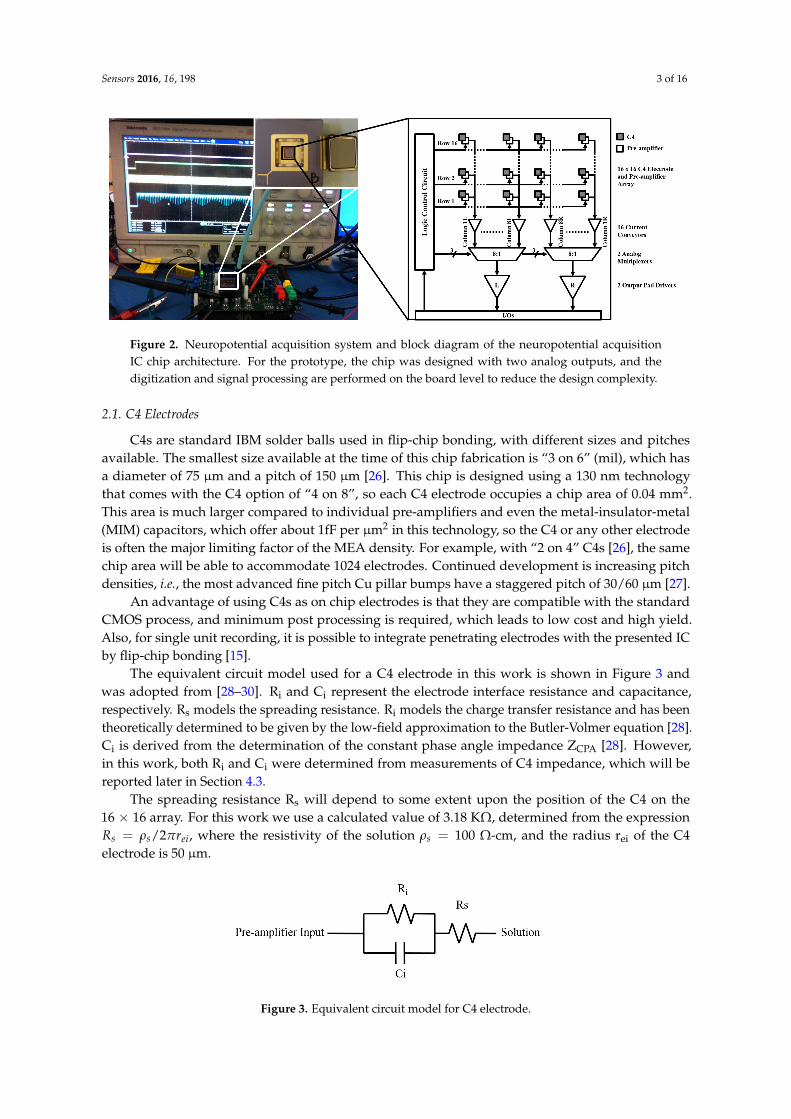
The architecture of the neuropotential recording IC chip is shown in Figure 2. The active MEA has256 on-chip C4 electrodes for extracellular recording, occupying an area of 3.2 mm × 3.2 mm (activearea), or 25 electrodes per mm2. Each C4 electrode is capacitively-coupled to a low-noise pre-amplifierto form an input channel. The AC coupling can prevent the system from becoming saturated bythe half-cell potential of the electrode contacts. Sixteen rows are selected sequentially by an on-chipcounter, and two analog multiplexers are used to select one of eight columns on both the left and rightsides. At any given time, only one column on each side of the chip (left and right) is connected toan output channel, and thus only two output channels are needed for the 256 input channels. In thefollowing sections, an input channel row x, column y on the left side will be referred as input (x, yL).Testing was performed on a custom-designed printed circuit board (PCB).
Sensors 2016, 16, 198 3 of 16
Figure 2. Neuropotential acquisition system and block diagram of the neuropotential acquisitionIC chip architecture. For the prototype, the chip was designed with two analog outputs, and thedigitization and signal processing are performed on the board level to reduce the design complexity.
2.1. C4 Electrodes
C4s are standard IBM solder balls used in flip-chip bonding, with different sizes and pitchesavailable. The smallest size available at the time of this chip fabrication is “3 on 6” (mil), which hasa diameter of 75 µm and a pitch of 150 µm [26]. This chip is designed using a 130 nm technologythat comes with the C4 option of “4 on 8”, so each C4 electrode occupies a chip area of 0.04 mm2.This area is much larger compared to individual pre-amplifiers and even the metal-insulator-metal(MIM) capacitors, which offer about 1fF per µm2 in this technology, so the C4 or any other electrodeis often the major limiting factor of the MEA density. For example, with “2 on 4” C4s [26], the samechip area will be able to accommodate 1024 electrodes. Continued development is increasing pitchdensities, i.e., the most advanced fine pitch Cu pillar bumps have a staggered pitch of 30/60 µm [27].
An advantage of using C4s as on chip electrodes is that they are compatible with the standardCMOS process, and minimum post processing is required, which leads to low cost and high yield.Also, for single unit recording, it is possible to integrate penetrating electrodes with the presented ICby flip-chip bonding [15].
The equivalent circuit model used for a C4 electrode in this work is shown in Figure 3 andwas adopted from [28–30]. Ri and Ci represent the electrode interface resistance and capacitance,respectively. Rs models the spreading resistance. Ri models the charge transfer resistance and has beentheoretically determined to be given by the low-field approximation to the Butler-Volmer equation [28].Ci is derived from the determination of the constant phase angle impedance ZCPA [28]. However,in this work, both Ri and Ci were determined from measurements of C4 impedance, which will bereported later in Section 4.3.
The spreading resistance Rs will depend to some extent upon the position of the C4 on the16 × 16 array. For this work we use a calculated value of 3.18 KΩ, determined from the expressionRs = ρs/2πrei, where the resistivity of the solution ρs = 100 Ω-cm, and the radius rei of the C4electrode is 50 µm.
Figure 3. Equivalent circuit model for C4 electrode.

Sensors 2016, 16, 198 4 of 16
2.2. Low-Noise Preamplifier
The circuit schematic of the pre-amplifier array is shown in Figure 4. Each pre-amplifier from thearray is a single-ended input PMOS cascode amplifier. The input of each pre-amplifier is AC coupledto the C4 recording electrode through a 10 pF MIM capacitor Cin. The input of the pre-amplifier is alsoDC coupled to a fixed voltage V1 (i.e., 1.8 V) through a high-impedance pseudo-resistor M0 to providebiasing. The PMOS pseudo-resistor can achieve a GΩ-TΩ resistance value R0 with transistor M0’s gatebiased in the sub-threshold region [18,22], or even in the accumulation region [31]. The low frequencycorner fL of the pre-amplifier is determined by the dominant capacitor Cin and the pseudo-resistor R0.Its equation is given by
fL =1
2πCinR0(1)
The function of the calibration cell will be discussed in Section 2.4.To achieve the desired fL value, a larger R0 allows the use of a smaller input coupling capacitor.
Theoretically, to the first-order approximation,with a TΩ resistor, a 160 fF capacitor is enough to achieve a 1 Hz low frequency corner. A
single-ended input topology with a high resistance pseudo-resistor doesn’t rely on large valuecapacitors, and thus allows this approach to take advantage of further scaling.
Figure 4. Circuit schematic of the pre-amplifier array. The calibration cell has the same size as a regularpre-amplifier, only without being connected to a C4 input electrode. There is one calibration cell oneach column. The substrates of NMOS and PMOS devices are connected to the ground and the 2.5 Vpower supply, respectively.
The input-referred thermal noise voltage of the pre-amplifier is:
v2n =
8kT3gm1
· (1 + 2 · gm3
gm1) · ∆ f (2)
Therefore, to reduce the thermal noise, a large gm1 and a small gm3 is desired. In terms oftransistor size, a larger gate width over a length ratio of M1 (100 µm / 0.48 µm) was used, compared toM3 (10 µm/5 µm). There is a trade-off between minimizing the thermal noise and the 1/f noise, sincethe latter requires a small gm1 value.
The input-referred root mean square (rms) noise voltage is calculated using the noise frequencycurve by
vrms =
√∫ 10kHz
10Hz
v2n
∆ fd f (3)
which gives 3.99 µVrms.
Sensors 2016, 16, 198 5 of 16
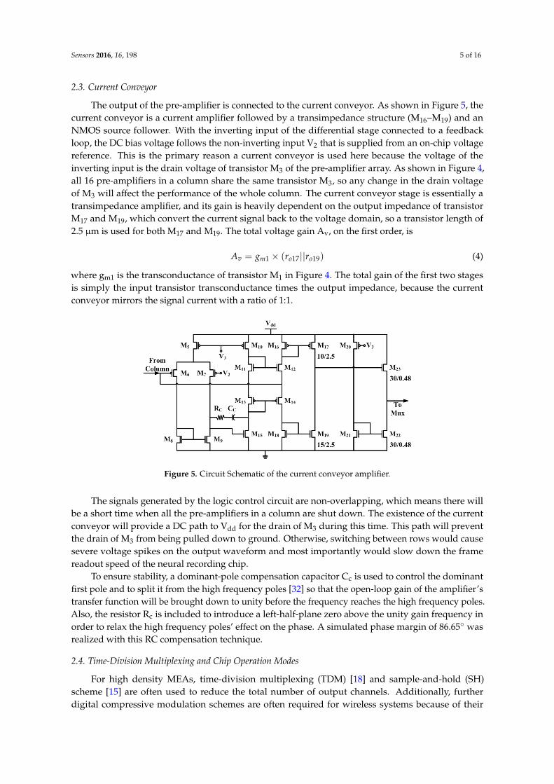
2.3. Current Conveyor
The output of the pre-amplifier is connected to the current conveyor. As shown in Figure 5, thecurrent conveyor is a current amplifier followed by a transimpedance structure (M16–M19) and anNMOS source follower. With the inverting input of the differential stage connected to a feedbackloop, the DC bias voltage follows the non-inverting input V2 that is supplied from an on-chip voltagereference. This is the primary reason a current conveyor is used here because the voltage of theinverting input is the drain voltage of transistor M3 of the pre-amplifier array. As shown in Figure 4,all 16 pre-amplifiers in a column share the same transistor M3, so any change in the drain voltageof M3 will affect the performance of the whole column. The current conveyor stage is essentially atransimpedance amplifier, and its gain is heavily dependent on the output impedance of transistorM17 and M19, which convert the current signal back to the voltage domain, so a transistor length of2.5 µm is used for both M17 and M19. The total voltage gain Av, on the first order, is
Av = gm1 × (ro17||ro19) (4)
where gm1 is the transconductance of transistor M1 in Figure 4. The total gain of the first two stagesis simply the input transistor transconductance times the output impedance, because the currentconveyor mirrors the signal current with a ratio of 1:1.
Figure 5. Circuit Schematic of the current conveyor amplifier.
The signals generated by the logic control circuit are non-overlapping, which means there willbe a short time when all the pre-amplifiers in a column are shut down. The existence of the currentconveyor will provide a DC path to Vdd for the drain of M3 during this time. This path will preventthe drain of M3 from being pulled down to ground. Otherwise, switching between rows would causesevere voltage spikes on the output waveform and most importantly would slow down the framereadout speed of the neural recording chip.
To ensure stability, a dominant-pole compensation capacitor Cc is used to control the dominantfirst pole and to split it from the high frequency poles [32] so that the open-loop gain of the amplifier’stransfer function will be brought down to unity before the frequency reaches the high frequency poles.Also, the resistor Rc is included to introduce a left-half-plane zero above the unity gain frequency inorder to relax the high frequency poles’ effect on the phase. A simulated phase margin of 86.65 wasrealized with this RC compensation technique.
2.4. Time-Division Multiplexing and Chip Operation Modes
For high density MEAs, time-division multiplexing (TDM) [18] and sample-and-hold (SH)scheme [15] are often used to reduce the total number of output channels. Additionally, furtherdigital compressive modulation schemes are often required for wireless systems because of their
Sensors 2016, 16, 198 6 of 16
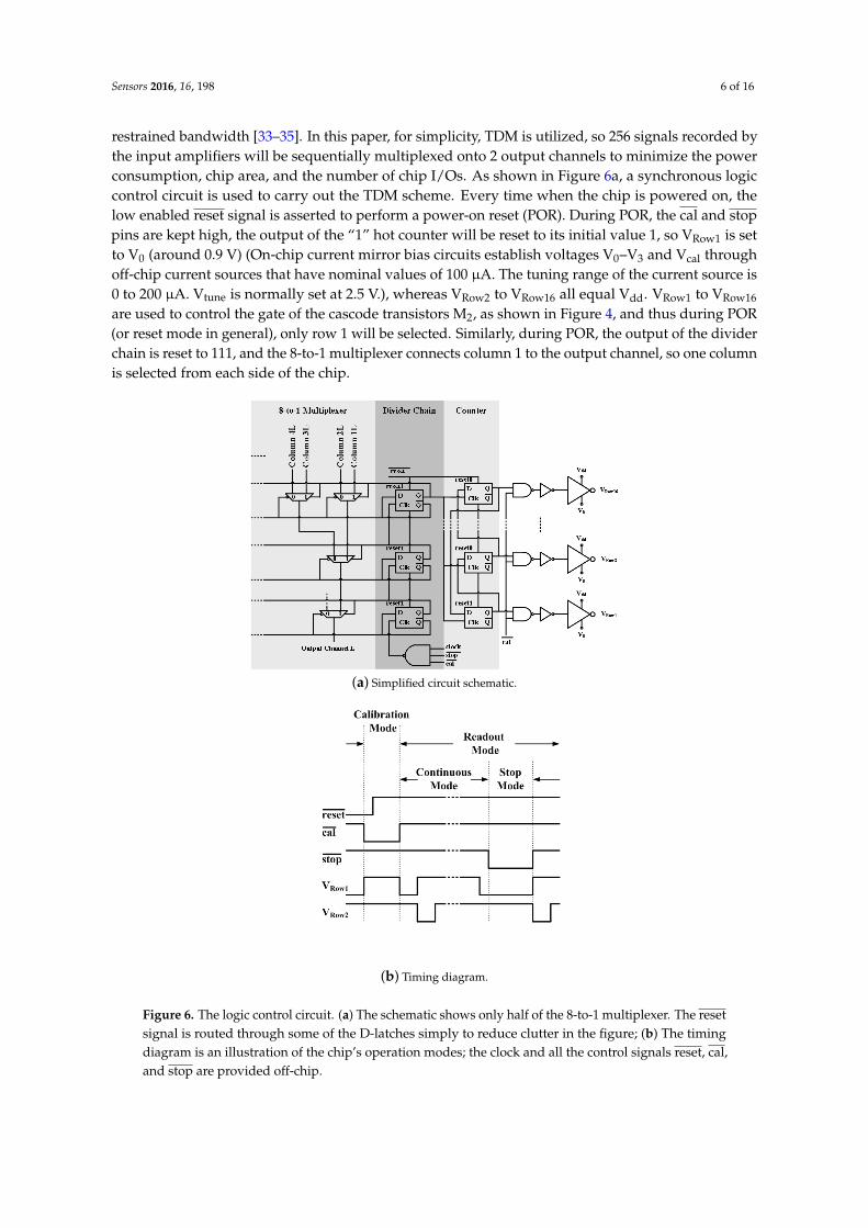
restrained bandwidth [33–35]. In this paper, for simplicity, TDM is utilized, so 256 signals recorded bythe input amplifiers will be sequentially multiplexed onto 2 output channels to minimize the powerconsumption, chip area, and the number of chip I/Os. As shown in Figure 6a, a synchronous logiccontrol circuit is used to carry out the TDM scheme. Every time when the chip is powered on, thelow enabled reset signal is asserted to perform a power-on reset (POR). During POR, the cal and stoppins are kept high, the output of the “1” hot counter will be reset to its initial value 1, so VRow1 is setto V0 (around 0.9 V) (On-chip current mirror bias circuits establish voltages V0–V3 and Vcal throughoff-chip current sources that have nominal values of 100 µA. The tuning range of the current source is0 to 200 µA. Vtune is normally set at 2.5 V.), whereas VRow2 to VRow16 all equal Vdd. VRow1 to VRow16
are used to control the gate of the cascode transistors M2, as shown in Figure 4, and thus during POR(or reset mode in general), only row 1 will be selected. Similarly, during POR, the output of the dividerchain is reset to 111, and the 8-to-1 multiplexer connects column 1 to the output channel, so one columnis selected from each side of the chip.
(a) Simplified circuit schematic.
(b) Timing diagram.
Figure 6. The logic control circuit. (a) The schematic shows only half of the 8-to-1 multiplexer. The resetsignal is routed through some of the D-latches simply to reduce clutter in the figure; (b) The timingdiagram is an illustration of the chip’s operation modes; the clock and all the control signals reset, cal,and stop are provided off-chip.

Sensors 2016, 16, 198 7 of 16
After POR, the reset pin is deasserted, the output of the divider-chain will count from 111 to 000every 8 clock cycles, whereas the output of the counter repeats from 1 to 16 every 128 clock cycles.Thus, a consecutive input channel is selected every clock cycle, from input (1, 1) to (16, 8). Since at anygiven time only one of the M2 transistors in a column is selected, all the pre-amplifiers in a columncan share the same tail-current. As a result, the power consumption of the pre-amplifier array isreduced by a factor of 16. This is the continuous mode. The clock is designed to operate at 2.56 MHz incontinuous mode, so each input channel will be selected every 128 clock cycles, for a 20 kHz samplingrate per channel (The design scan rate of 2.56 MHz has not been achieved in testing due to the impactof process variation. This will be discussed in Section 4).
The chip can also operate in two additional modes: stop mode and calibration mode. Pullingdown the stop pin will enable the stop mode, whereby the clock will be superseded, interruptingthe TDM. Thus, stop mode allows observation in real time of any channel from each half of the chip.Continuous mode is resumed once the stop signal is disabled. After every reset, a calibration oftenneeds to be performed. As mentioned previously, the pseudo-resistor enables the recording of LFPswith small input capacitors. However, this high resistance value results in a relatively large RC timeconstant, which slows down the process of charging and discharging the gate of the M1 transistor. Inorder to accelerate this process, the cal signal is used to turn on M0 to convert the pseudo-resistor into alow resistance state to acquire a desirable RC time constant that can calibrate the gate voltage of M1 toV1 efficiently. During calibration, the gate of M2Cal (as shown in Figure 4) will be pulled down to V0 toactivate the calibration pre-amplifiers, while all the regular pre-amplifiers are disabled. The purpose ofthe calibration pre-amplifiers is to avoid the drain voltage of M3 being pulled down to ground duringcalibration. By keeping the drain voltage of M3 stable, it is possible to increase the switching speedbetween operation modes. The timing diagram of the operation modes is plotted in Figure 6b.
3. Fabrication and Packaging
The neural recording chip was designed and fabricated in IBM 0.13 µm BiCMOS 8HP technology(No bipolar devices were used in the chip in order to keep the design CMOS compatible). It has a totalarea of 4 mm × 4 mm and a recording area (active area) of 3.2 mm × 3.2 mm. A micrograph of thechip is shown in Figure 1. The C4 electrodes are standard “4 on 8” (mil), 100 µm in diameter with a200 µm pitch. Their material composition is 97% Pb (lead) and 3% Sn (tin) (Lead free version of C4sare also available with 97.7% Sn and 2.3% Ag (silver). Scheduling issues necessitated using Pb-basedC4s on this chip). To improve the C4 electrode biocompatibility, gold was plated onto the C4s usingBright Electroless Gold solution (Transene Company, Inc.) [36,37]. The photographs of C4s before andafter Au electrolessplating are shown in Figure 1.
In order to accommodate the different requirements of electrical, in vitro, and in vivo testing, thefabricated chips were wire bonded to three different packages (Quik-Pak) [38], as shown in Figure 7.For electrical testing, a 10 × 10 ceramic PGA package was used to provide direct access to inputchannels (1, 3L), (1, 3R), (7, 1R), and (16, 3R) that were pre-wired to the chip pads with the top levelmetal, as shown in Figure 1. For in vitro applications, the neural recording chip was packaged in anopen-top PGA package with bonding wires encapsulated for mechanical and electrical protection. Thefinished package has all the C4 electrodes exposed in order to interface with the brain/tissue slices,and a plastic fluidic chamber was built on top of the PGA package. An important function of thein vitro testing package is to provide a way to apply signals to all 256 input channels.
A 6 mm × 7 mm custom PCB package was also built to carry out acute in vivo experimentsin living rats. The diameter of a rat brain cross-section is not much bigger than 1 cm, so the majorrequirement of the in vivo package is that it has to be able to fit on top of the rat brain. Meanwhile,it has to be connected to the recording side with a minimum number of wire connections withoutcompletely constraining the rat under test. In order to do so, the chip was wire bonded to the top sideof the PCB with the bond wires encapsulated. The height of the epoxy was milled down to 100 µmafter the encapsulation for better contact between the electrodes and rat brain. A 0.3 mm pitch, 17 pin

Sensors 2016, 16, 198 8 of 16
flat flexible cable (FFC) was chosen as the interconnection between the in vivo package and a recordingPCB. The width of the FFC was 5.1 mm, which is slightly smaller than the width of the PCB package,and is thin and flexible, all of which makes the FFC suitable for acute in vivo testing.
Figure 7. Chip packaging: A standard 10 × 10 ceramic PGA (Top left), an open-top 10 × 10 ceramicPGA (Top middle), front side of the custom printed circuit board (PCB) package (Top right), back sideof the custom PCB package (Bottom right), and flat flexible cables (FFC) (Bottom middle).
4. Chip Characterization
4.1. Electrical Testing
4.1.1. System Voltage Gain
The electrical testing package was used to characterize the voltage gain of a single input channel.Figure 8 shows the measurement when the IC is operating in continuous mode at the maximum framerate of 20 kHz. 128 inputs (per side) were scanned with only one input channel connected to thefunction generator. A sinusoidal signal with a peak-to-peak amplitude of 1 mV and a frequency of1 kHz was applied to input channel (1, 3L) through an subminiature version A (SMA) connector. Allthe other input channels were left floating. The sine wave at the output can be seen in the highlightedenvelope of the selected cell with the provided input. Calculation using the amplitude of the waveformenvelope gives a voltage gain of 58.1 dB.
Figure 8. Measured output waveform from the recording chip in continuous mode with a samplingrate of 20 kHz. The envelope of a single channel that had a 1 kHz sinusoidal input is highlighted withthe dashed line.

Sensors 2016, 16, 198 9 of 16
All 128 input channels on the left side of the chip were measured in stop mode using the in vitrotesting package. The output DC voltage level of each input channel was manually adjusted to 1.5 V.The mean and standard deviation of the voltage gain of the 128 inputs on the left side of the chip were58.7 dB and 0.37 dB, respectively.
4.1.2. Process Variation
Semiconductor process variation is the deviation of the manufactured device or interconnectparameters from their designed or expected nominal values. It can cause mismatch in current mirrors,different input recording channels, and threshold voltage variations. As a result, the chip outputDC level will vary from channel to channel. In order for the neuropotential recording chip to workproperly, the output DC level needs to be corrected for each individual input channel. This can bedone by adjusting the off-chip current sources as shown in Figure 9. However, to operate the chip incontinuous mode, the variation correction process needs to be integrated into the recording PCB sothat during every clock cycle a proper bias current will be applied to the chip to automatically calibratethe DC voltage value of the output channel.
Figure 9. Bias current values to set the output DC level of each individual input channel to 1.5 V acrossthe entire chip.
Currently, we are using a microcontroller to provide a clock signal to the MEA chip, as well as tocontrol the bias current value. Ideally, this should be performed on-chip to prevent the I/O interfacelatency, which determines how fast the bias current can be changed and limits the clock’s maximumfrequency. Figure 10 shows the measured results from preliminary work on the process variationcorrection PCB system. The output voltage of the chip is digitized and used to control the chip’s biascurrent. At t = 0, since Vout is smaller than 1.5 V, the feedback increases the bias current by 0.1 µA perstep, which in turn increases the output DC voltage (Vout ramp at 0.3 s in Figure 10). At 0.32 s, theoutput DC voltage reaches 1.5 V, and the feedback system locks and holds the bias current constant.This calibration procedure is done once at power-on, and the corresponding Ibias0 values for each inputare recorded in the microcontroller for use in the continuous mode testing operation. However, thisoff-chip method requires an excessive amount of time to adjust the output offset for each individualinput during the continuous mode, so the continuous mode feature cannot be operated at the expected10 kHz rate.

Sensors 2016, 16, 198 10 of 16
Figure 10. A demonstration of automatic correction for a single channel in stop mode.
4.1.3. Frequency Response and Noise Performance
The frequency response and input-referred noise voltage spectral density of the neural recordingIC were measured with both electrical and in vitro testing packages using an oscilloscope and aspectrum analyzer, respectively. The stimulus was provided to the IC through an SMA connection.As shown in Figure 11, the system frequency response has a high frequency cutoff of 1.4 MHz. The lowfrequency corner is below 0.05 Hz, which is beyond the range of our spectrum analyzer, indicatingthat the pseudo-resistor has a resistance value greater than 0.32 TΩ. The input-referred noise spectrumwas measured in stop mode, and the integrated input-referred noise voltage is 4.6 µVrms for a 10 Hzto 10 kHz bandwidth. As a result of the process variation issue, this measurement could not be donein the continuous mode at a 20 kHz sampling rate, due to the length of time required to center theoutput for each input channel. Therefore, the measurements reported here do not include any potentialcontribution from noise folding, clock noise, and crosstalk.
(a)
(b)
Figure 11. Measured system (a) frequency response; and (b) input-referred noise.
Sensors 2016, 16, 198 11 of 16
4.2. Electrical Testing With the In Vitro Package
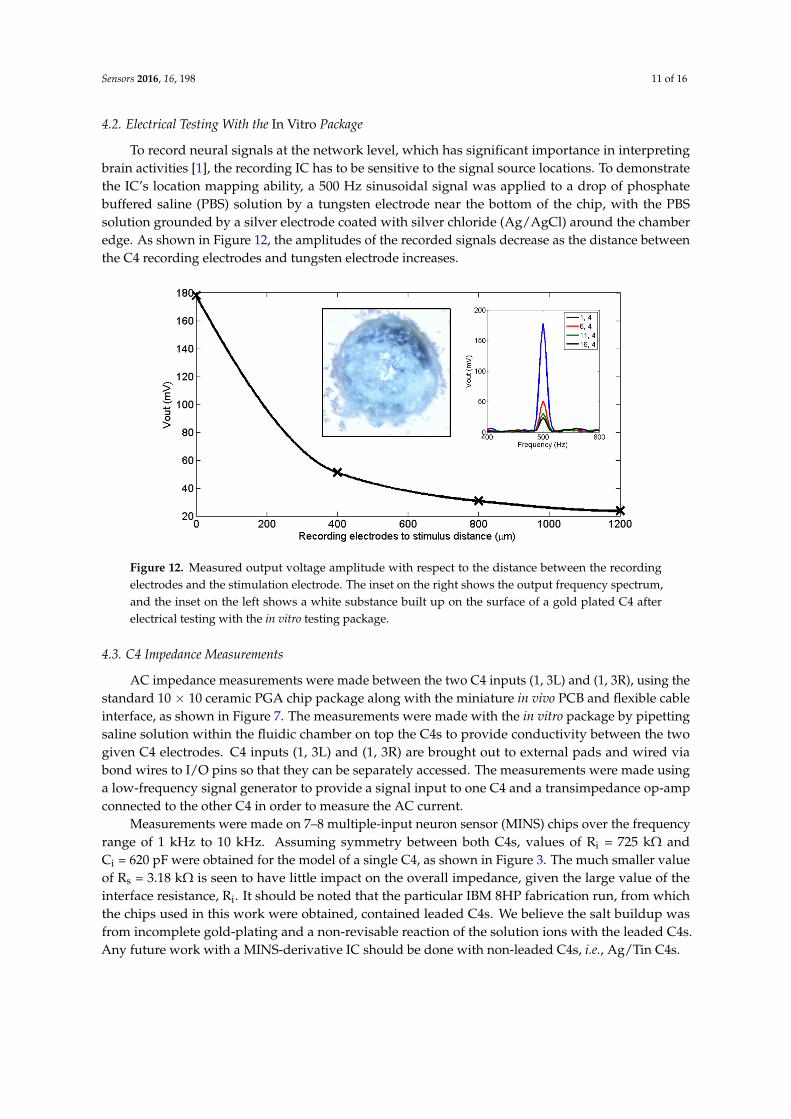
To record neural signals at the network level, which has significant importance in interpretingbrain activities [1], the recording IC has to be sensitive to the signal source locations. To demonstratethe IC’s location mapping ability, a 500 Hz sinusoidal signal was applied to a drop of phosphatebuffered saline (PBS) solution by a tungsten electrode near the bottom of the chip, with the PBSsolution grounded by a silver electrode coated with silver chloride (Ag/AgCl) around the chamberedge. As shown in Figure 12, the amplitudes of the recorded signals decrease as the distance betweenthe C4 recording electrodes and tungsten electrode increases.
Figure 12. Measured output voltage amplitude with respect to the distance between the recordingelectrodes and the stimulation electrode. The inset on the right shows the output frequency spectrum,and the inset on the left shows a white substance built up on the surface of a gold plated C4 afterelectrical testing with the in vitro testing package.
4.3. C4 Impedance Measurements
AC impedance measurements were made between the two C4 inputs (1, 3L) and (1, 3R), using thestandard 10 × 10 ceramic PGA chip package along with the miniature in vivo PCB and flexible cableinterface, as shown in Figure 7. The measurements were made with the in vitro package by pipettingsaline solution within the fluidic chamber on top the C4s to provide conductivity between the twogiven C4 electrodes. C4 inputs (1, 3L) and (1, 3R) are brought out to external pads and wired viabond wires to I/O pins so that they can be separately accessed. The measurements were made usinga low-frequency signal generator to provide a signal input to one C4 and a transimpedance op-ampconnected to the other C4 in order to measure the AC current.
Measurements were made on 7–8 multiple-input neuron sensor (MINS) chips over the frequencyrange of 1 kHz to 10 kHz. Assuming symmetry between both C4s, values of Ri = 725 kΩ andCi = 620 pF were obtained for the model of a single C4, as shown in Figure 3. The much smaller valueof Rs = 3.18 kΩ is seen to have little impact on the overall impedance, given the large value of theinterface resistance, Ri. It should be noted that the particular IBM 8HP fabrication run, from whichthe chips used in this work were obtained, contained leaded C4s. We believe the salt buildup wasfrom incomplete gold-plating and a non-revisable reaction of the solution ions with the leaded C4s.Any future work with a MINS-derivative IC should be done with non-leaded C4s, i.e., Ag/Tin C4s.

Sensors 2016, 16, 198 12 of 16
5. Acute Rat Cortical Recording
5.1. Surgical Procedure
The fabricated array was tested in a Sprague-Dawley rat (∼400 g) under ketamine and xylazine(80 mg/kg and 12 mg/kg, respectively, IP) anesthesia. All procedures were approved and performedin accordance with the guidelines of the Institutional Animal Care and Use Committee, RutgersUniversity, Newark, NJ. The fur over the skull was shaved, and the animal was placed in a stereotaxicframe. The body temperature was kept at around 36 C with the help of a heating pad under theanimal. The blood oxygenation was continuously observed with a pulse oximeter from the hindpaw while the animal breathed spontaneously. The skull over the barrel cortex was removed in a4 mm × 4 mm rectangular area on the right side. The dura was cut and reflected over to expose thecortical surface. Normal saline was applied to keep the cortex moist. The array was attached to astainless steel rod in the middle of its top surface using medical epoxy (Figure 13). The array wasattached to a micromanipulator by the metal rod for easy positioning and mechanical stability. Thereference electrode was a platinum wire soldered to the array ground and dipped into the saline poolaround the array. The array was slowly lowered until all contacts (C4 bumps) were touching thebarrel cortex.
Figure 13. Illustration of the rat cortical recording setup.
5.2. Recording Procedures
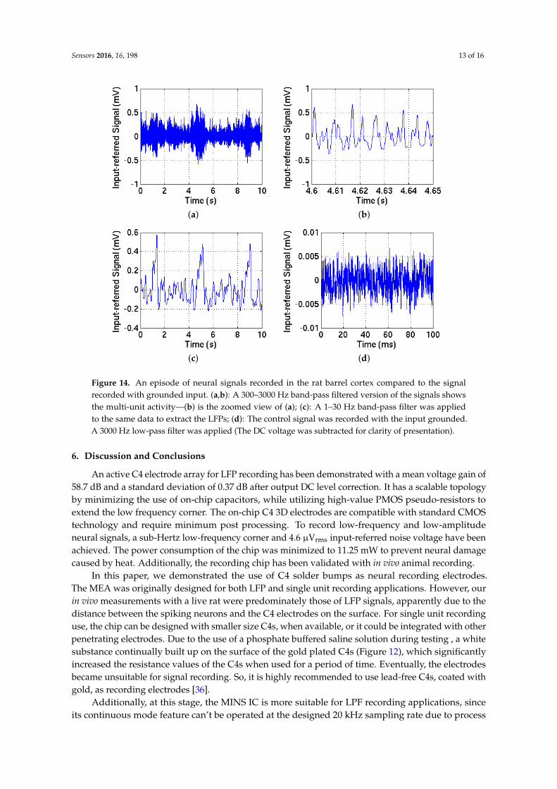
The multiplexed outputs of the recording array were connected to a National Instruments DataAcquisition Board (PCI-6071), and the neural signals were acquired at 20 kHz in 10 s episodes intoa desktop computer. Another Matlab code initialized the board and selected one of the 256 contactsfor neural recording. Multi-unit activity, as well as LFPs, were recorded as shown in Figure 14a,b,respectively. All the data were collected within an hour after performing the surgical procedure onthe rat. Visible C4 imprints were observed on the surface of the rat brain after recording. The controlsignal (Figure 14d) was recorded with the input grounded through a PCB connector. The control signalis two orders of magnitude smaller than the measured LFP signals.
Sensors 2016, 16, 198 13 of 16
(a) (b)
(c) (d)
Figure 14. An episode of neural signals recorded in the rat barrel cortex compared to the signalrecorded with grounded input. (a,b): A 300–3000 Hz band-pass filtered version of the signals showsthe multi-unit activity—(b) is the zoomed view of (a); (c): A 1–30 Hz band-pass filter was appliedto the same data to extract the LFPs; (d): The control signal was recorded with the input grounded.A 3000 Hz low-pass filter was applied (The DC voltage was subtracted for clarity of presentation).
6. Discussion and Conclusions
An active C4 electrode array for LFP recording has been demonstrated with a mean voltage gain of58.7 dB and a standard deviation of 0.37 dB after output DC level correction. It has a scalable topologyby minimizing the use of on-chip capacitors, while utilizing high-value PMOS pseudo-resistors toextend the low frequency corner. The on-chip C4 3D electrodes are compatible with standard CMOStechnology and require minimum post processing. To record low-frequency and low-amplitudeneural signals, a sub-Hertz low-frequency corner and 4.6 µVrms input-referred noise voltage have beenachieved. The power consumption of the chip was minimized to 11.25 mW to prevent neural damagecaused by heat. Additionally, the recording chip has been validated with in vivo animal recording.
In this paper, we demonstrated the use of C4 solder bumps as neural recording electrodes.The MEA was originally designed for both LFP and single unit recording applications. However, ourin vivo measurements with a live rat were predominately those of LFP signals, apparently due to thedistance between the spiking neurons and the C4 electrodes on the surface. For single unit recordinguse, the chip can be designed with smaller size C4s, when available, or it could be integrated with otherpenetrating electrodes. Due to the use of a phosphate buffered saline solution during testing , a whitesubstance continually built up on the surface of the gold plated C4s (Figure 12), which significantlyincreased the resistance values of the C4s when used for a period of time. Eventually, the electrodesbecame unsuitable for signal recording. So, it is highly recommended to use lead-free C4s, coated withgold, as recording electrodes [36].
Additionally, at this stage, the MINS IC is more suitable for LPF recording applications, sinceits continuous mode feature can’t be operated at the designed 20 kHz sampling rate due to process

Sensors 2016, 16, 198 14 of 16
variation. The future goal is to improve the channel sampling rate in continuous mode, so that theMINS IC can fully take advantage of the spatial resolution of the high density MEA, which is crucialfor studying neural function at the network level. Preliminary work (Section 4.1.2) showed that theprocess variation error can be corrected by adjusting the IC bias current with off-chip real-time dataacquisition and feedback circuits. However, the sampling rate is limited by the IC interface, whichlargely depends on the loading from the IC package and external components. Future iterations ofthe IC could include on-chip digitally programmable current trimming circuitry to avoid the timingoverhead of communicating with off-chip circuits. Thus, it is feasible to scan the entire 256 channelsin 50 µs (20 kHz sampling rate) and acquire the spatial information of neural activities recorded incontinuous mode.
Finally, it became apparent from our measurements that the ability to adjust the gain of therecording channels would be of considerable value to prevent signals from saturation at the output.Such a gain adjustment could easily be integrated into the design of the MINS IC.
7. Future Work
For suggested future work, process variation correction circuitry can be integrated on-chip toimprove the continuous mode scanning rate and reduce noise coupling to the bias current from thePCB. Also, the gain of the chip could be reduced to 40 dB (or preferably, made adjustable) for a betterpower/performance tradeoff, to reduce the power density, and to prevent the output signal fromsaturating for larger input signals. To further reduce the power density, the tail current should beturned off when a column is idle, and turned back on one cycle before the column is selected. Lead-freeversions of C4s will be used to replace leaded C4s, and studies on the chronic effects of C4s on livinganimals will be carried out.
Acknowledgments: This work was funded by NIH/NINDS under Grant 1R01 NS072385. The chip wasfabricated at IBM Microelectronics through a MOSIS Educational Program (MEP)/Research license. The electricalmeasurements were carried out in Allyn Hubbard’s VNNS Lab at Boston University with the help ofHoward Cohen. The animal experiment was carried out with Ammar Abdo and Gokhan Ordek’s help inSahin’s Neural Interface Lab at New Jersey Institute of Technology. The authors also want to thank Alex Higueraat Boston University for her contribution to the C4 modeling.
Author Contributions: Lu Wang, David Freedman, and Ronald Knepper conceived and designed the circuit;M. Selim Ünlü and David Freedman developed the chip post-processing procedure. Lu Wang, David Freedman,and Ronald Knepper designed and performed the electrical experiments; Lu Wang and Mesut Sahin designed andperformed the in vivo experiments. Lu Wang and David Freedman analyzed the data; Lu Wang, David Freedman,Ronald Knepper, and Mesut Sahin wrote the paper.
Conflicts of Interest: The authors declare no conflict of interest.
References
1. Hochberg, L.R.; Bacher, D.; Jarosiewicz, B.; Masse, N.Y.; Simeral, J.D.; Vogel, J.; Haddadin, S.; Liu, J.;Cash, S.S.; van der Smagt, P.; et al. Reach and grasp by people with tetraplegia using a neurally controlledrobotic arm. Nature 2012, 485, 372–375.
2. Obien, M.; Deligkaris, K.; Bullmann, T.; Bakkum, D.; Frey, U. Revealing neuronal function throughmicroelectrode array recordings. Front. Neurosci. 2015, 8, doi:10.3389/fnins.2014.00423.
3. Imfeld, K.; Garenne, A.; Martinoia, S.; Koudelka-Hep, M.; Berdondini, L. Motivations and APS-basedsolution for high-resolution extracellular recording from in-vitro neuronal networks. In Proceedings of the3rd International IEEE/EMBS Conference on Neural Engineering, Kohala Coast, HI, USA, 2–5 May 2007;pp. 225–228.
4. Prasad, A.; Sahin, M. Can motor volition be extracted from the spinal cord? J. NeuroEng. Rehabil. 2012,9, 372–375.
5. Ordek, G.; Groth, J.D.; Sahin, M. Differential effects of ketamine/xylazine anesthesia on the cerebral andcerebellar cortical activities in the rat. J. Neurophysi. 2013, 109, 1435–1443.
6. Engel, A.K.; Moll, C.K.E.; Fried, I.; Ojemann, G.A. Invasive recordings from the human brain: Clinicalinsights and beyond. Nature Rev. Neurosci. 2005, 6, 35–47.

Sensors 2016, 16, 198 15 of 16
7. Buzsaki, G.; Anastassiou, C.A.; Koch, C. The origin of extracellular fields and currents—EEG, ECoG, LFPand spikes. Nature Rev. Neurosci. 2012, 13, 407–420.
8. Shulyzki, R.; Abdelhalim, K.; Bagheri, A.; Salam, M.; Florez, C.; Velazquez, J.; Carlen, P.; Genov, R.320-Channel Active Probe for High-Resolution Neuromonitoring and Responsive Neurostimulation.IEEE Trans. Biomed. Circuits Syst. 2014, 9, 34–49.
9. Harrison, R.R. The design of integrated circuits to observe brain activity. IEEE Proc. 2008. 96, 1213–1216.10. Eversmann, B.; Jenkner, M.; Hofmann, F.; Paulus, C.; Brederlow, R.; Holzapfl, B.; Fromherz, P.; Merz, M.;
Brenner, M.; Schreiter, M.; et al. A 128 × 128 CMOS biosensor array for extracellular recording of neuralactivity. IEEE J. Solid State Circuits 2003, 38, 2306–2317.
11. Frey, U.; Heer, F.; Pedron, R.; Hafizovic, S.; Greve, F.; Sedivy, J.; Kirstein, K.; Hierlemann, A. An 11k-electrode126-channel high-density microelectrode array to interact with electrogenic cells. In Proceedings of the IEEEInternational Solid-State Circuits Conference (ISSCC’07), San Francisco, CA, USA, 11–15 February 2007;pp. 158–159.
12. Imfeld, K.; Neukom, S.; Maccione, A.; Bornat, Y.; Martinoia, S.; Farine, P.A.; Koudelka-Hep, M.; Berdondini, L.Large-scale, high-resolution data acquisition system for extracellular recording of electrophysiologicalactivity. IEEE Trans. Biomed. Eng. 2008, 55, 2064–2073.
13. Nordhausen, C.T.; Maynard, E.M.; Normann, R.A. Single unit recording capabilities of a 100-microelectrodearray. Brain Res. 1996, 726, 129–140.
14. Frieswijk, T.A.; Bielen, J.A.; Rutten, W.L.C.; Bergveld, P. Development of a solder bump technique forcontacting a three-dimensional multi electrode array. Microsyst. Technol. 1997, 3, 48–52.
15. Aziz, J.N.Y.; Abdelhalim, K.; Shulyzki, R.; Genov, R.; Bardakjian, B.L.; Derchansky, M.; Serletis, D.; Carlen, P.L.256-channel neural recording and delta compression microsystem with 3D electrodes. IEEE J. Solid StateCircuits 2009, 44, 995–1005.
16. Song, Y.K.; Borton, D.; Park, S.; Patterson, W.; Bull, C.; Laiwalla, F.; Mislow, J.; Simeral, J.; Donoghue, J.;Nurmikko, A. Active Microelectronic Neurosensor Arrays for Implantable Brain Communication Interfaces.IEEE Trans. Neural Syst. Rehabil. Eng. 2009, 17, 339–345.
17. Gao, H.; Walker, R.; Nuyujukian, P.; Makinwa, K.; Shenoy, K.; Murmann, B.; Meng, T. HermesE: A 96-ChannelFull Data Rate Direct Neural Interface in 0.13 µm CMOS. IEEE J. Solid State Circuits 2012, 47, 1043–1055.
18. Sodagar, A.M.; Perlin, G.E.; Yao, Y.; Najafi, K.; Wise, K.D. An implantable 64-channel wireless microsystemfor single-unit neural recording. IEEE J. Solid State Circuits 2009, 44, 2591–2604.
19. Bagheri, A.; Gabran, S.; Salam, M.; Perez Velazquez, J.; Mansour, R.; Salama, M.; Genov, R. Massively-ParallelNeuromonitoring and Neurostimulation Rodent Headset With Nanotextured Flexible Microelectrodes.IEEE Trans. Biomed. Circuits Syst. 2013, 7, 601–609.
20. Gabran, S.; Salam, M.; Dian, J.; El-Hayek, Y.; Velazquez, J.; Genov, R.; Carlen, P.; Salama, M.; Mansour, R.High-Density Intracortical Microelectrode Arrays With Multiple Metallization Layers for Fine-ResolutionNeuromonitoring and Neurostimulation. IEEE Trans. Neural Syst. Rehabil. Eng. 2013, 21, 869–879.
21. Lopez, C.; Andrei, A.; Mitra, S.; Welkenhuysen, M.; Eberle, W.; Bartic, C.; Puers, R.; Yazicioglu, R.;Gielen, G. An Implantable 455-Active-Electrode 52-Channel CMOS Neural Probe. IEEE J. Solid StateCircuits 2014, 49, 248–261.
22. Harrison, R.R.; Charles, C. A low-power low-noise CMOS amplifier for neural recording applications. IEEE J.Solid State Circuits 2003, 38, 958–965.
23. Yun, X.; Kim, D.; Stanacevic, M.; Mainen, Z. Low-Power High-Resolution 32-channel Neural RecordingSystem. In Proceedings of the 29th Annual International Conference of the IEEE Engineering in Medicineand Biology Society (EMBC’07), Lyon, France, 22–26 August 2007; pp. 2373–2376.
24. Wattanapanitch, W.; Sarpeshkar, R. A Low-Power 32-Channel Digitally Programmable Neural RecordingIntegrated Circuit. IEEE Trans. Biomed. Circuits Syst. 2011, 5, 592–602.
25. Han, D.; Zheng, Y.; Rajkumar, R.; Dawe, G.; Je, M. A 0.45 V 100-Channel Neural-Recording IC WithSub-µW/Channel Consumption in 0.18 µm CMOS. In Proceedings of the 2013 IEEE International Solid-StateCircuits Conference Digest of Technical Papers (ISSCC), San Francisco, CA, USA, 17–21 February 2013;Volume 7, pp. 735–746.

Sensors 2016, 16, 198 16 of 16
26. Wright, S.; Polastre, R.; Gan, H.; Buchwalter, L.; Horton, R.; Andry, P.; Sprogis, E.; Patel, C.; Tsang, C.;Knickerbocker, J.; et al. Characterization of micro-bump C4 interconnects for Si-carrier SOP applications.In Proceedings of the 56th Electronic Components and Technology Conference, San Diego, CA, USA,30 May–2 June 2006; pp. 633–640.
27. Wen, S.; Park, K.; Thompson, P.; Shirley, D.; Lee, J.; Park, H. Flip chip assembly with advanced RDLtechnology. In Proceedings of the 2013 14th International Conference on Electronic Packaging Technology(ICEPT), Dalian, China, 11–14 August 2013; pp. 57–59.
28. Frank, W.; Schenker, I.; Schmutz, P.; Hierlemann, A. Impedance Characterization and Modeling of Electrodesfor Biomedical Applications. IEEE Trans. Biomed. Eng. 2005, 52, 1295–1302.
29. Joye, N.; Schmid, A.; Leblebici, Y. Electrical Modeling of the Cell-Electrode Interface for Recording NeuralActivity from High-Density Microelectrode Arrays. Neurocomput. Elsevier 2009, 73, 250–259.
30. Higuera, A. Neural Interface Model for a Pt/Au C4 Bump Microelectrode Array. Unpublished work, 2016.31. Wang, L.; Freedman, D.S.; Knepper, R.W.; Ünlü, M.S.; Sahin, M. A 16 × 16 Multi-electrode Array with
Integrated CMOS Amplifiers for Neural Signal Recording. In Proceedings of the 2011 IEEE BiomedicalCircuits and Systems Conference (BioCAS), San Diego, CA, USA, 10–12 November 2011; pp. 82–85.
32. Carusone, T.C.; Johns, D.A.; Martin, K.W. Analog Integrated Circuit Design, 2nd ed.; John Wiley & Sons:Hoboken, NJ, USA, 2011.
33. Majidzadeh, V.; Schmid, A.; Leblebici, Y. A 16-channel 220 µW neural recording IC with embedded deltacompression. In Proceedings of the 2011 IEEE Biomedical Circuits and Systems Conference (BioCAS),San Diego, CA, USA, 10–12 November 2011; pp. 9–12.
34. Hosseini-Nejad, H.; Jannesari, A.; Sodagar, A. Data Compression in Brain-Machine/Computer InterfacesBased on the Walsh-Hadamard Transform. IEEE Trans. Biomed. Circuits Syst. 2014, 8, 129–137.
35. Yazdani, N.; Rashidi, A.; Sodagar, A.M.; Mohebbi, M. Reduction of spatial data redundancy in implantablemulti-channel neural recording microsystems. In Proceedings of the 2014 IEEE Biomedical Circuits andSystems Conference (BioCAS), Lausanne, Switzerland, 22–24 October 2014; pp. 208–211.
36. Berdondini, L.; Wal, P.D.V.D.; Rooij, N.F.D.; Koudelka-Hep, M. Development of an electroless post-processingtechnique for depositing gold as electrode material on CMOS devices. Sens. Actuators B Chem. 2004,99, 505–510.
37. Aziz, J.N.Y.; Genov, R.; Bardakjian, B.L.; Derchansky, M.; Carlen, P.L. Brain-silicon interface forhigh-resolution in vitro neural recording. IEEE Trans. Biomed. Circuits Syst. 2007, 1, 56–62.
38. Graham, A.H.D.; Bowen, C.R.; Surguy, S.M.; Robbins, J.; Taylor, J. New prototype assembly methods forbiosensor integrated circuits. Med. Eng. Phys. 2011, 33, 973–979.
c© 2016 by the authors; licensee MDPI, Basel, Switzerland. This article is an open accessarticle distributed under the terms and conditions of the Creative Commons by Attribution(CC-BY) license (http://creativecommons.org/licenses/by/4.0/).