ACT50 Rev1 APPLICATION CIRCUIT ACT50 Rev1, 5/2007 Green Power Off-Line PWM Controller...
14
Innovative Products. Active Solutions. - 1 - www.active-semi.com Copyright © 2007 Active-Semi, Inc Active-Semi Proprietary–For Authorized Recipients and Customers SIMPLIFIED APPLICATION CIRCUIT ACT50 Rev1, 5/2007 Green Power Off-Line PWM Controller ActiveSwitcher TM IC Family FEATURES • Less than 300mW Standby Power: Exceeds the Lastest CEC, Blue Angle and Energy Star Requirements • Supports NPN Emitter-Drive for Lowest Total Solution Cost • Fast Response Current Mode PWM • Very Low Line/Load Regulation • 60kHz Switching Frequency • Line Compensation • Programmable Current Limit • 50μA Start Up Current • Tiny SOT23-5 and DIP-8 Packages • 30W Output Power without Heat Sink with DIP-8 Package APPLICATIONS • Battery Chargers • Power Adapters • Standby Power Supplies • Appliances • Universal Off-Line Power Supplies GENERAL DESCRIPTION The ACT50 is a compact, high performance off-line power supply controller that is ideal for use in the next generation high performance universal input adapters and chargers. The ACT50 features an ad- vanced current-mode PWM control architecture that achieves the smallest form-factor and fast transient response yet requires less than 300mW of standby power, surpassing even the latest requirements of the California Energy Commission (CEC), the Euro- pean Union Blue Angel, and US Energy Star stan- dards. The ACT50 is optimized for use in the flyback topol- ogy, and requires just a low cost optocoupler and reference device, such as the ‘431, to provide fully adjustable CC/CV operation. This device additionally features a proprietary low EMI driver that can be compatible with both external MOSFET and NPN transistors, and supports emit- ter-switching to achieve the lowest possible solution cost. The ACT50 is available in tiny SOT23-5 or DIP-8 packages.
-
Upload
truongduong -
Category
Documents
-
view
217 -
download
4
Transcript of ACT50 Rev1 APPLICATION CIRCUIT ACT50 Rev1, 5/2007 Green Power Off-Line PWM Controller...

Innovative Products. Active Solutions. - 1 - www.active-semi.com
Copyright © 2007 Active-Semi, Inc Active-Semi Proprietary–For Authorized Recipients and Customers
SIMPLIFIED APPLICATION CIRCUIT
ACT50 Rev1, 5/2007
Green Power Off-Line PWM Controller ActiveSwitcherTM IC Family
FEATURES • Less than 300mW Standby Power:
Exceeds the Lastest CEC, Blue Angle and Energy Star Requirements
• Supports NPN Emitter-Drive for Lowest Total Solution Cost
• Fast Response Current Mode PWM • Very Low Line/Load Regulation • 60kHz Switching Frequency • Line Compensation • Programmable Current Limit • 50µA Start Up Current • Tiny SOT23-5 and DIP-8 Packages • 30W Output Power without Heat Sink with
DIP-8 Package
APPLICATIONS • Battery Chargers • Power Adapters • Standby Power Supplies • Appliances • Universal Off-Line Power Supplies
GENERAL DESCRIPTION The ACT50 is a compact, high performance off-line power supply controller that is ideal for use in the next generation high performance universal input adapters and chargers. The ACT50 features an ad-vanced current-mode PWM control architecture that achieves the smallest form-factor and fast transient response yet requires less than 300mW of standby power, surpassing even the latest requirements of the California Energy Commission (CEC), the Euro-pean Union Blue Angel, and US Energy Star stan-dards.
The ACT50 is optimized for use in the flyback topol-ogy, and requires just a low cost optocoupler and reference device, such as the ‘431, to provide fully adjustable CC/CV operation.
This device additionally features a proprietary low EMI driver that can be compatible with both external MOSFET and NPN transistors, and supports emit-ter-switching to achieve the lowest possible solution cost.
The ACT50 is available in tiny SOT23-5 or DIP-8 packages.

ACT50 Rev1, 5/2007
Innovative Products. Active Solutions. - 2 - www.active-semi.com
Copyright © 2007 Active-Semi, Inc Active-Semi Proprietary–For Authorized Recipients and Customers
ORDERING INFORMATION
PIN CONFIGURATION
PIN DESCRIPTIONS
PART NUMBER TEMPERATURE RANGE PACKAGE PINS PACKING ACT50UC-T -40°C to 85°C SOT23-5 5 TAPE & REEL
ACT50DH -40°C to 85°C DIP-8 8 TUBE
PIN NUMBER PIN NAME
SOT23-5 DIP-8 1 3 VDD Supply Input. VDD is internally clamped at 16.5V.
2 1 G Ground.
– 4 GP Power Ground. Always connect this pin to G (for DIP-8 package only).
3 2 FB Feedback Input. Current flows out of FB into the optocoupler.
PIN DESCRIPTION
4 8 ISET Current Limit Programming Pin. Connect an external resistor from ISET to G to program the current limit.
5 5 SW Emitter Driver Switching Node.
SOT23-5 DIP-8
ACT50DH
5
6
7
81
2
3
4
G
FB
VDD
GP
ISET
N/C
N/C
SW
ACT50DH

ACT50 Rev1, 5/2007
Innovative Products. Active Solutions. - 3 - www.active-semi.com
Copyright © 2007 Active-Semi, Inc Active-Semi Proprietary–For Authorized Recipients and Customers
ABSOLUTE MAXIMUM RATINGS
(VVDD = VVDDON, TA = 25°C, unless otherwise specified.)
PARAMETER VALUE UNIT VDD to G -0.3 to +16.5 V
VDD Current 20 mA
FB, ISET to G -0.3 to +6 V
SW to G -0.3 to +18 V
Continuous SW Current 1.8 A
Junction to Ambient Thermal Resistance (θJA) SOT23-5 190
°C/W DIP-8 105
Maximum Power Dissipation (Derate 5.3mW/°C above TA = 50°C) SOT23-5 0.4
DIP-8 1
Operating Junction Temperature -40 to 150 °C
Storage Temperature -55 to 150 °C
W
: Do not exceed these limits to prevent damage to the device. Exposure to absolute maximum rating conditions for long periods may affect device reliability.
ELECTRICAL CHARACTERISTICS
PARAMETER SYMBOL TEST CONDITIONS MIN TYP MAX UNIT VDD Turn-On Voltage VDDON Rising edge 14 15 16 V
VDD Turn-Off Voltage VDDOFF Falling edge 10 11 12 V
VDD Clamp Voltage VDDCLAMP IDD = 5mA VDDON + 1 VDDON + 1.5 VDDON + 2 V
Supply Current
IDDSU Before turn on 50 100 µA
IDD After turn on, RISET = 25kΩ 0.9 2 mA
IDDHICCUP Hiccup and before turn on 70 140 µA
Switching Frequency fSW 45 60 75 kHz
ISET Voltage VISET RISET = 25kΩ 1.8 2 2.2 V
FB Open Loop Clamp Voltage VFBC IFB = 0mA, RISET = 25kΩ 2.8 3.2 3.6 V
FB Input Impedance ZFB VFB = 3.2V 4 kΩ
FB Bias Current IFB VFB = 0V, RISET = 25kΩ 500 800 µA
Maximum Duty Cycle DMAX ISW = 10mA 67 75 83 %
Minimum Duty Cycle DMIN ISW = 100mA 3.5 %
Current Limit ILIM RISET = 25kΩ 1.2 1.5 1.8
A RISET = 50kΩ 0.45 0.6 0.75
Switch On-Resistance RSW ISW = 100mA 1 Ω
SW Rise Time tR 1nF load, 15Ω pull-up 60 ns
SW Fall Time tF 1nF load, 15Ω pull-up 40 ns
SW Switch Off Current ISWOFF Switch in off-state, VSW = 20V 1 10 µA
ACT50 Rev1, 5/2007
Innovative Products. Active Solutions. - 4 - www.active-semi.com
Copyright © 2007 Active-Semi, Inc Active-Semi Proprietary–For Authorized Recipients and Customers
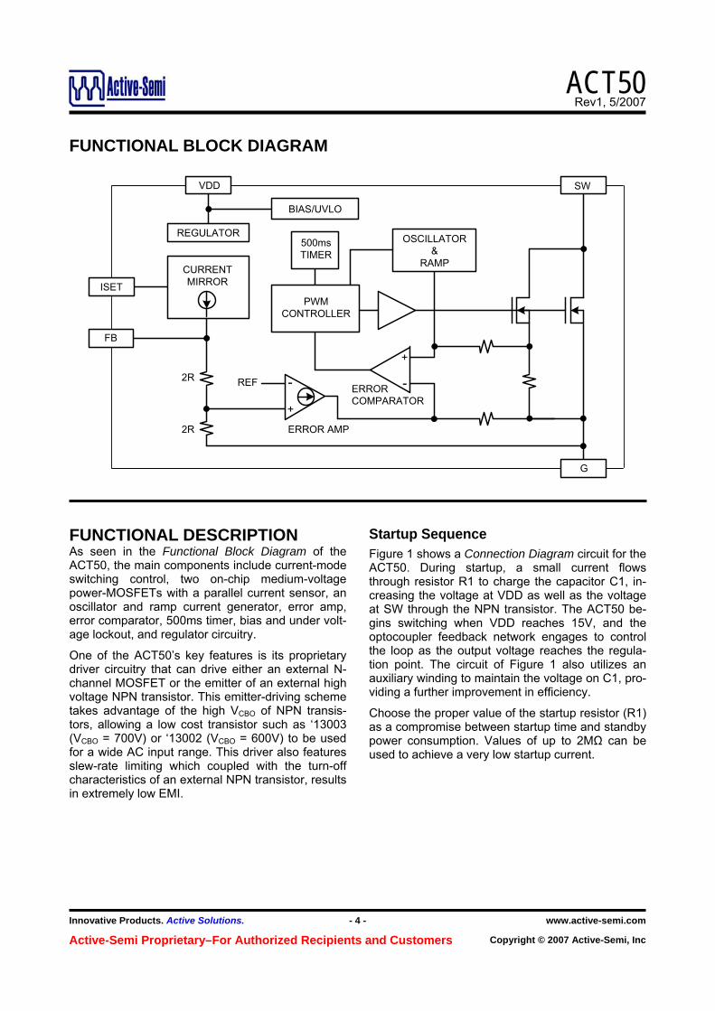
FUNCTIONAL BLOCK DIAGRAM
G
SWVDD
ISET
FB
2R
2R
ERROR AMP
+
-REF
PWMCONTROLLER
500msTIMER
BIAS/UVLO
REGULATOR
CURRENTMIRROR
+
-
OSCILLATOR&
RAMP
ERROR COMPARATOR
FUNCTIONAL DESCRIPTION As seen in the Functional Block Diagram of the ACT50, the main components include current-mode switching control, two on-chip medium-voltage power-MOSFETs with a parallel current sensor, an oscillator and ramp current generator, error amp, error comparator, 500ms timer, bias and under volt-age lockout, and regulator circuitry.
One of the ACT50’s key features is its proprietary driver circuitry that can drive either an external N-channel MOSFET or the emitter of an external high voltage NPN transistor. This emitter-driving scheme takes advantage of the high VCBO of NPN transis-tors, allowing a low cost transistor such as ‘13003 (VCBO = 700V) or ‘13002 (VCBO = 600V) to be used for a wide AC input range. This driver also features slew-rate limiting which coupled with the turn-off characteristics of an external NPN transistor, results in extremely low EMI.
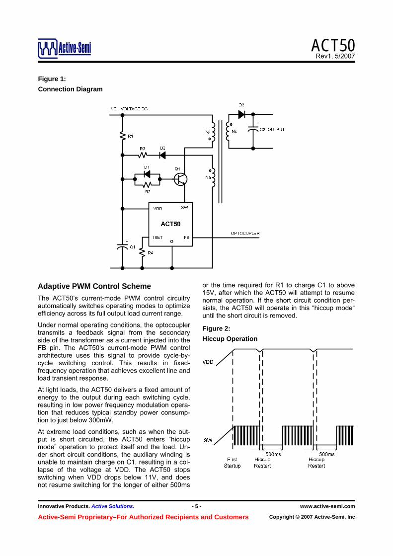
Startup Sequence Figure 1 shows a Connection Diagram circuit for the ACT50. During startup, a small current flows through resistor R1 to charge the capacitor C1, in-creasing the voltage at VDD as well as the voltage at SW through the NPN transistor. The ACT50 be-gins switching when VDD reaches 15V, and the optocoupler feedback network engages to control the loop as the output voltage reaches the regula-tion point. The circuit of Figure 1 also utilizes an auxiliary winding to maintain the voltage on C1, pro-viding a further improvement in efficiency.
Choose the proper value of the startup resistor (R1) as a compromise between startup time and standby power consumption. Values of up to 2MΩ can be used to achieve a very low startup current.
ACT50 Rev1, 5/2007
Innovative Products. Active Solutions. - 5 - www.active-semi.com
Copyright © 2007 Active-Semi, Inc Active-Semi Proprietary–For Authorized Recipients and Customers
Figure 1: Connection Diagram
Adaptive PWM Control Scheme The ACT50’s current-mode PWM control circuitry automatically switches operating modes to optimize efficiency across its full output load current range.
Under normal operating conditions, the optocoupler transmits a feedback signal from the secondary side of the transformer as a current injected into the FB pin. The ACT50’s current-mode PWM control architecture uses this signal to provide cycle-by-cycle switching control. This results in fixed-frequency operation that achieves excellent line and load transient response.
At light loads, the ACT50 delivers a fixed amount of energy to the output during each switching cycle, resulting in low power frequency modulation opera-tion that reduces typical standby power consump-tion to just below 300mW.
At extreme load conditions, such as when the out-put is short circuited, the ACT50 enters “hiccup mode” operation to protect itself and the load. Un-der short circuit conditions, the auxiliary winding is unable to maintain charge on C1, resulting in a col-lapse of the voltage at VDD. The ACT50 stops switching when VDD drops below 11V, and does not resume switching for the longer of either 500ms
or the time required for R1 to charge C1 to above 15V, after which the ACT50 will attempt to resume normal operation. If the short circuit condition per-sists, the ACT50 will operate in this “hiccup mode“ until the short circuit is removed.
Figure 2: Hiccup Operation

ACT50 Rev1, 5/2007
Innovative Products. Active Solutions. - 6 - www.active-semi.com
Copyright © 2007 Active-Semi, Inc Active-Semi Proprietary–For Authorized Recipients and Customers
APPLICATIONS INFORMATION External Power Transistor The ACT50 allows a low cost high voltage power NPN transistor such as ‘13003 or ‘13002 to be used safely in flyback configuration. The required collec-tor voltage rating for VAC = 265V with full output load is at least 600V to 700V. As seen from Figure 3, the breakdown voltage of an NPN transistor is significantly improved when it is driven at its emitter. Table 1 lists the breakdown voltage of some tran-sistors appropriate for use with the ACT50.
Table 1: Recommended Power Transistor List
Figure 3: NPN Transistor Reverse Bias Safe Operation Area
Output Power The maximum power that can be delivered from the ACT50 depends on several factors including the AC line voltage, the power handling capability of the external high voltage transistor, the thermal design of the system, and transformer construction.
The maximum output power is a function of the cur-rent limit, which is programmed by connecting an external resistor (RISET) from ISET to G. Refer to Figure 4 for more information about the relationship between current limit and RISET.
Figure 4: Current Limit vs. RISET
Output Voltage Setting The output voltage is set by resistors R7 and R8, as shown in Figure 5. If the ‘431 generates a 2.5V ref-erence voltage, the output voltage is given by:
DEVICE VCBO VCEO IC hFEMIN PACKAGE MJE13002 600V 300V 1.5A 8 TO-126
MJE13003, KSE13003 700V 400V 1.5A 8 TO-126
STX13003 700V 400V 1A 8 TO-92
20 30 40 50 60 70 80 90 100
0
0.2
0.4
0.6
0.8
1.0
1.2
1.4
1.6
1.8 C
urre
nt L
imit
(A)
RISET (kΩ)
AC
T50-001
( ) 8R/8R7RV5.2VOUT += (1)

ACT50 Rev1, 5/2007
Innovative Products. Active Solutions. - 7 - www.active-semi.com
Copyright © 2007 Active-Semi, Inc Active-Semi Proprietary–For Authorized Recipients and Customers
Layout Consideration The following should be observed when doing lay-out for the ACT50:
1) Use a “star point “ connection at the G pin of ACT50 for the VDD bypass components, the input filter capacitor and other ground connec-tions on the primary side.
2) Keep the loop across the input filter capacitor, the transformer primary windings, the high volt-age transistor, and the ACT50 as small as pos-sible.
3) Keep the trace between the ACT50’s SW pin and the high voltage transistor emitter pin as short as possible.
4) Keep the loop across the secondary windings, the output diode, and the output capacitors as small as possible.
5) Allow enough copper area under the high volt-age transistor, output diode, and current shunt resistor for heat sink.
Figure 5: 24W Adapter Application Using ACT50
D1D3
D2 D4
1N4007'4
+
1
2
3
4
R11M 1206
R21M 1206
C1 104/275V
VR1 TVR05471
F11A/250V
MR1DC K053
AC IN
PUT
LF1UU 10.530mH
C2
33µF/400V
R3 24
k
R5 75
0kR6
300k
+
R4 2
4k C522µF/35V
IC1ACT50
R9 100
R8 100
D7 4148
1-48
3
C6 103/
25V
IC 3BOPTO
5
2C7 10
2/50
V
C447PF/1kV
D5FR 107
R11 100
R10100k/2W
C3102/1kV
R7 4.7 D6 4148
Q113003
18T
TRANSFORMER
CY1222/400V
15T
85T
C8102/100V
R1222
D8
MBR 10100+C9
470µF/16V+
12V2A
GND
C10330µF/16V
LF2T9'5'4
R13510
IC2TL431
R173k
R15 33kC11
334/25V
IC3AOPTO
R14200
R1612k
AC IN
PUT

ACT50 Rev1, 5/2007
Innovative Products. Active Solutions. - 8 - www.active-semi.com
Copyright © 2007 Active-Semi, Inc Active-Semi Proprietary–For Authorized Recipients and Customers
TYPICAL PERFORMANCE CHARACTERISTICS
VDD Turn-On Voltage vs. Temperature
VD
D T
urn-
Off
Vol
tage
(V)
12
AC
T50-002 125 50 25 0 -20 -45
13
14
15
16
17
18
Temperature (°C)
8
AC
T50-003
125 50 25 0 -20
9
10
11
12
13
14
Temperature (°C)
VDD Clamp Voltage vs. Temperature
VD
D C
lam
p V
olta
ge (V
)
13.5
AC
T50-004
125 50 25 0 -20 -45
14.5
15.5
16.5
17.5
18.5
19.5
Temperature (°C)
Supply Current vs. Temperature
Sup
ply
Cur
rent
(mA
)
0.6
AC
T50-005
125 50 25 0 -20 -45
0.7
0.8
0.9
1.0
1.1
1.2
Temperature (°C)
(RISET = 25kΩ unless otherwise specified.)
70 85 100
VDD Turn-Off Voltage vs. Temperature
70 85 100
VD
D T
urn-
Off
Vol
tage
(V)
70 85 100 70 85 100
Sta
rtup
Sup
ply
Cur
rent
(µA
) 80
70
50
60
40
30
20 -45 -20 0 25 50 70 85 100 125 -45 -20 0 25 50 70 85 100 125
50
80
70
60
40
30
20
Hic
cup
Sup
ply
Cur
rent
(µA
)
Startup Supply Current vs. Temperature Hiccup Supply Current vs. Temperature
AC
T50-006
AC
T50-007
Temperature (°C) Temperature (°C)
-45

ACT50 Rev1, 5/2007
Innovative Products. Active Solutions. - 9 - www.active-semi.com
Copyright © 2007 Active-Semi, Inc Active-Semi Proprietary–For Authorized Recipients and Customers
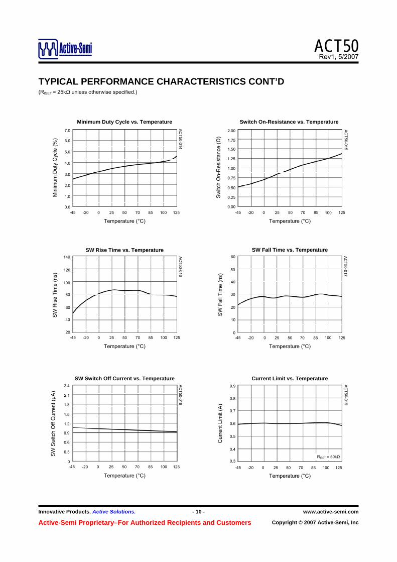
TYPICAL PERFORMANCE CHARACTERISTICS CONT’D
FB Input Impedance vs. Temperature
AC
T50-011
FB Open Voltage vs. Temperature
AC
T50-010
Maximum Duty Cycle vs. Temperature
AC
T50-013
FB Bias Current vs. Temperature
AC
T50-012
ISET Voltage vs. Temperature
AC
T50-009
Switching Frequency vs. Temperature
AC
T50-008
(RISET = 25kΩ unless otherwise specified.)
125 50 25 0 -20
Temperature (°C)
70 85 100 30
FB O
pen
Loop
Cla
mp
Vol
tage
(V)
40
50
60
70
80
90
1.7
ISE
T V
olta
ge (V
)
1.9
2.0
2.1
2.2
2.3
1.8
125 50 25 0 -20
Temperature (°C) 70 85 100
2.9
3.0
3.1
3.2
3.3
3.4
3.5
125 50 25 0 -20 -45
Temperature (°C) 70 85 100
1.0
2.0
3.0
4.0
5.0
6.0
125 50 25 0 -20 70 85 100
Temperature (°C)
125 50 25 0 -20 -45
Temperature (°C) 70 85 100
200
300
400
500
600
700
800 90
125 50 25 0 -20 -45
Temperature (°C) 70 85 100
85
80
75
70
65
60
-45
FB In
put I
mpe
danc
e (kΩ
)
Sw
itchi
ng F
requ
ency
(kH
z)
FB B
ias
Cur
rent
(µA
)
Max
imum
Dut
y C
ycle
(%)
-45 -45
7.0
ACT50 Rev1, 5/2007
Innovative Products. Active Solutions. - 10 - www.active-semi.com
Copyright © 2007 Active-Semi, Inc Active-Semi Proprietary–For Authorized Recipients and Customers
RISET = 50kΩ
TYPICAL PERFORMANCE CHARACTERISTICS CONT’D
SW Fall Time vs. Temperature
AC
T50-017
SW Rise Time vs. Temperature
AC
T50-016
Current Limit vs. Temperature
AC
T50-019
SW Switch Off Current vs. Temperature
AC
T50-018
Switch On-Resistance vs. Temperature
AC
T50-015
Minimum Duty Cycle vs. Temperature
AC
T50-014
(RISET = 25kΩ unless otherwise specified.)
125 50 25 0 -20 -45
Temperature (°C) 70 85 100
Min
imum
Dut
y C
ycle
(%)
0.50
Sw
itch
On-
Res
ista
nce
(Ω)
1.00
1.25
1.50
1.75
2.00
0.75
125 50 25 0 -20 -45
Temperature (°C) 70 85 100
20
40
60
80
100
120
140
125 50 25 0 -20 -45
Temperature (°C)
70 85 100 0
10
20
30
40
50
60
125 50 25 0 -20 70 85 100
Temperature (°C)
125 50 25 0 -20 -45
Temperature (°C)
70 85 100
0.6
0.9
1.2
1.5
1.8
2.1
2.4
125 50 25 0 -20 -45
Temperature (°C) 70 85 100
0.9
0.8
0.7
0.6
0.5
0.4
0.3
-45
7.0
6.0
5.0
4.0
3.0
2.0
1.0
0.0
0.25
0.00
SW
Fal
l Tim
e (n
s)
SW
Ris
e Ti
me
(ns)
0
SW
Sw
itch
Off
Cur
rent
(µA
)
Cur
rent
Lim
it (A
)
0.3

ACT50 Rev1, 5/2007
Innovative Products. Active Solutions. - 11 - www.active-semi.com
Copyright © 2007 Active-Semi, Inc Active-Semi Proprietary–For Authorized Recipients and Customers
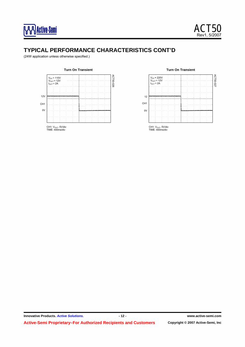
TYPICAL PERFORMANCE CHARACTERISTICS CONT’D
Start Up Delay Time
AC
T50-023
Start Up Delay Time
AC
T50-022
Turn On Transient
AC
T50-025
Turn On Transient
AC
T50-024
Load Transient
AC
T50-021
Load Transient
AC
T50-020
(24W application unless otherwise specified.)
CH1
CH2
CH1
12V
CH1
0V
12V
CH1
0V
CH1: VOUT, 200mV/div (AC COUPLED) TIME: 20ms/div
VAC = 110V VOUT = 12V IOUT = 0 to 2A
VAC = 220V VOUT = 12V IOUT = 0 to 2A
VAC = 110V VOUT = 12V IOUT = 2A
VAC = 220V VOUT = 12V IOUT = 2A
VAC = 220V VOUT = 12V IOUT = 2A
VAC = 110V VOUT = 12V IOUT = 2A
CH1: VOUT, 200mV/div (AC COUPLED) TIME: 20ms/div
CH1
CH1: Line Input, 200V/div CH2: VOUT, 10V/div TIME: 1s/div
CH1
CH2
CH1: Line Input, 500V/div CH2: VOUT, 10V/div TIME: 1s/div
CH1: VOUT, 5V/div TIME: 400ms/div
CH1: VOUT, 5V/div TIME: 400ms/div
ACT50 Rev1, 5/2007
Innovative Products. Active Solutions. - 12 - www.active-semi.com
Copyright © 2007 Active-Semi, Inc Active-Semi Proprietary–For Authorized Recipients and Customers
TYPICAL PERFORMANCE CHARACTERISTICS CONT’D
Turn On Transient Turn On Transient
AC
T50-026
(24W application unless otherwise specified.)
VAC = 110V VOUT = 12V IOUT = 2A
12V
CH1
0V
12
CH1
0V
VAC = 220V VOUT = 12V IOUT = 2A
AC
T50-027
CH1: VOUT, 5V/div TIME: 400ms/div
CH1: VOUT, 5V/div TIME: 400ms/div

ACT50 Rev1, 5/2007
Innovative Products. Active Solutions. - 13 - www.active-semi.com
Copyright © 2007 Active-Semi, Inc Active-Semi Proprietary–For Authorized Recipients and Customers
SYMBOL DIMENSION IN MILIMETERS
DIMENSION IN INCHES
MIN MAX MIN MAX A 1.050 1.250 0.041 0.049
A1 0.000 0.100 0.000 0.004
A2 1.050 1.150 0.041 0.045
b 0.300 0.400 0.012 0.016
c 0.100 0.200 0.004 0.008
D 2.820 3.020 0.111 0.119
E 1.500 1.700 0.059 0.067
E1 2.650 2.950 0.104 0.116
e 0.037 TYP
e1 1.800 2.000 0.071 0.079
L 0.700 REF 0.028 REF
L1 0.300 0.600 0.012 0.024
θ 0° 8° 0° 8°
0.950 TYP
PACKAGE OUTLINE SOT23-5 PACKAGE OUTLINE AND DIMENSIONS

ACT50 Rev1, 5/2007
Innovative Products. Active Solutions. - 14 - www.active-semi.com
Copyright © 2007 Active-Semi, Inc Active-Semi Proprietary–For Authorized Recipients and Customers
Active-Semi, Inc. reserves the right to modify the circuitry or specifications without notice. Users should evaluate each product to make sure that it is suitable for their applications. Active-Semi products are not intended or authorized for use as critical components in life-support devices or systems. Active-Semi, Inc. does not assume any liability arising out of the use of any product or circuit described in this data sheet, nor does it convey any patent license.
Active-Semi and its logo are trademarks of Active-Semi, Inc. For more information on this and other products, contact [email protected] or visit www.active-semi.com. For other inquiries, please send to:
1270 Oakmead Parkway, Suite 310, Sunnyvale, California 94085-4044, USA
PACKAGE OUTLINE
DIP-8 PACKAGE OUTLINE AND DIMENSIONS
SYMBOL DIMENSION IN MILIMETERS
DIMENSION IN INCHES
MIN MAX MIN MAX A 3.710 4.310 0.146 0.170
A1 0.510 0.020
A2 3.200 3.600 0.126 0.142
B 0.360 0.560 0.014 0.022
B1 1.524 TYP 0.060 TYP
C 0.204 0.360 0.008 0.014
D 9.000 9.400 0.354 0.370
E 6.200 6.600 0.244 0.260
E1 7.620 TYP 0.300 TYP
e 2.540 TYP 0.100 TYP
L 3.000 3.600 0.118 0.142
E2 8.200 9.400 0.323 0.370
e
B1B
A1
A2
LA
E2C
E1
D
E
![#001a Prinsip Dasar Analisis [2007.05.Lastest]](https://static.fdocuments.us/doc/165x107/5695d4291a28ab9b02a081ef/001a-prinsip-dasar-analisis-200705lastest.jpg)