
acs nn nn-2014-06469v 1. - Rutgers University
10
YAMAGUCHI ET AL. VOL. 9 ’ NO. 1 ’ 840 –849 ’ 2015 www.acsnano.org 840 December 18, 2014 C 2014 American Chemical Society Spatially Resolved Photoexcited Charge-Carrier Dynamics in Phase-Engineered Monolayer MoS 2 Hisato Yamaguchi, †,# Jean-Christophe Blancon, ‡,# Rajesh Kappera, § Sidong Lei, ) Sina Najmaei, ) Benjamin D. Mangum, ^ Gautam Gupta, † Pulickel M. Ajayan, ) Jun Lou, ) Manish Chhowalla, § Jared J. Crochet, ‡ and Aditya D. Mohite * ,† † MPA-11 Materials Synthesis and Integrated Devices, Materials Physics and Applications Division and ‡ C-PCS Physical Chemistry and Applied Spectroscopy, Chemistry Division, Los Alamos National Laboratory, Los Alamos, New Mexico 87545, United States, § Materials Science and Engineering, Rutgers University, Piscataway, New Jersey 08854, United States, ) Materials Science and NanoEngineering, Rice University, Houston, Texas 77005, United States, and ^ Pacific Light Technologies, Portland, Oregon 97201, United States. # These authors contributed equally to this work. G raphene has attracted much atten- tion in recent years due to its true two-dimensional (2D) geometry and one of the highest charge carrier mobility available for any material. 1 The bottleneck of its use in electronic and optoelectronic applications, however, lies in lack of an intrinsic band gap. 2 Graphene-based field effect transistors (FETs) do not turn off completely, and the lifetimes of photoex- cited carriers are too short for practical devices due to its semimetallic nature. 3 An emerging class of 2D nanomaterials, which has the complementary properties to that of graphene, is transition-metal dichalco- genides (TMDs). They have intrinsic band gaps in the visible range (12 eV) and relatively high charge carrier mobilities (few tens to hundreds of cm 2 /V s) that are expected to overcome the limitations of graphene-based optical, electronic, and optoelectronic 2D devices. 412 One of the key challenges in this field of research is to achieve ohmic contacts to TMD-based semiconductor devices in order to access intrinsic optoelectronic properties. Schottky contacts provide an extrinsic resistance to current flow and do not allow for a clean measurement of the semiconducting chan- nel performance. 1315 One accepted pro- cess to obtain low-resistance contacts to 2D TMDs such as MoS 2 at present is to use * Address correspondence to [email protected]. Received for review November 12, 2014 and accepted December 18, 2014. Published online 10.1021/nn506469v ABSTRACT A fundamental understanding of the intrinsic op- toelectronic properties of atomically thin transition-metal dichalco- genides (TMDs) is crucial for its integration into high performance semiconductor devices. Here, we investigate the transport properties of chemical vapor deposition (CVD) grown monolayer molybdenum disulfide (MoS 2 ) under photoexcitation using correlated scanning photocurrent microscopy and photoluminescence imaging. We examined the effect of local phase transformation underneath the metal electrodes on the generation of photocurrent across the channel length with diffraction-limited spatial resolution. While maximum photocurrent generation occurs at the Schottky contacts of semiconducting (2H- phase) MoS 2 , after the metallic phase transformation (1T-phase), the photocurrent peak is observed toward the center of the device channel, suggesting a strong reduction of native Schottky barriers. Analysis using the bias and position dependence of the photocurrent indicates that the Schottky barrier heights are a few millielectron volts for 1T- and ∼200 meV for 2H-contacted devices. We also demonstrate that a reduction of native Schottky barriers in a 1T device enhances the photoresponsivity by more than 1 order of magnitude, a crucial parameter in achieving high-performance optoelectronic devices. The obtained results pave a way for the fundamental understanding of intrinsic optoelectronic properties of atomically thin TMDs where ohmic contacts are necessary for achieving high-efficiency devices with low power consumption. KEYWORDS: MoS 2 . optoelectronic . scanning photocurrent microscopy . contact resistance . phase conversion . monolayer . transition-metal dichalcogenide ARTICLE
Transcript of acs nn nn-2014-06469v 1. - Rutgers University

YAMAGUCHI ET AL. VOL. 9 ’ NO. 1 ’ 840–849 ’ 2015
www.acsnano.org
840
December 18, 2014
C 2014 American Chemical Society
Spatially Resolved PhotoexcitedCharge-Carrier Dynamics inPhase-Engineered Monolayer MoS2Hisato Yamaguchi,†,# Jean-Christophe Blancon,‡,# Rajesh Kappera,§ Sidong Lei, ) Sina Najmaei, )
BenjaminD.Mangum,^GautamGupta,† PulickelM.Ajayan, ) Jun Lou, )Manish Chhowalla,§ Jared J. Crochet,‡
and Aditya D. Mohite*,†
†MPA-11 Materials Synthesis and Integrated Devices, Materials Physics and Applications Division and ‡C-PCS Physical Chemistry and Applied Spectroscopy,Chemistry Division, Los Alamos National Laboratory, Los Alamos, New Mexico 87545, United States, §Materials Science and Engineering, Rutgers University,Piscataway, New Jersey 08854, United States, )Materials Science and NanoEngineering, Rice University, Houston, Texas 77005, United States, and ^Pacific LightTechnologies, Portland, Oregon 97201, United States. #These authors contributed equally to this work.
Graphene has attracted much atten-tion in recent years due to its truetwo-dimensional (2D) geometry and
one of the highest charge carrier mobilityavailable for any material.1 The bottleneckof its use in electronic and optoelectronicapplications, however, lies in lack of anintrinsic band gap.2 Graphene-based fieldeffect transistors (FETs) do not turn offcompletely, and the lifetimes of photoex-cited carriers are too short for practicaldevices due to its semimetallic nature.3 Anemerging class of 2D nanomaterials, whichhas the complementary properties to thatof graphene, is transition-metal dichalco-genides (TMDs). They have intrinsic band
gaps in the visible range (1�2 eV) andrelatively high charge carrier mobilities(few tens to hundreds of cm2/V s) that areexpected to overcome the limitations ofgraphene-based optical, electronic, andoptoelectronic 2D devices.4�12 One of thekey challenges in this field of research isto achieve ohmic contacts to TMD-basedsemiconductor devices in order to accessintrinsic optoelectronic properties. Schottkycontacts provide an extrinsic resistance tocurrent flow and do not allow for a cleanmeasurement of the semiconducting chan-nel performance.13�15 One accepted pro-cess to obtain low-resistance contacts to2D TMDs such as MoS2 at present is to use
* Address correspondence [email protected].
Received for review November 12, 2014and accepted December 18, 2014.
Published online10.1021/nn506469v
ABSTRACT A fundamental understanding of the intrinsic op-
toelectronic properties of atomically thin transition-metal dichalco-
genides (TMDs) is crucial for its integration into high performance
semiconductor devices. Here, we investigate the transport properties
of chemical vapor deposition (CVD) grown monolayer molybdenum
disulfide (MoS2) under photoexcitation using correlated scanning
photocurrent microscopy and photoluminescence imaging. We
examined the effect of local phase transformation underneath the
metal electrodes on the generation of photocurrent across the
channel length with diffraction-limited spatial resolution. While maximum photocurrent generation occurs at the Schottky contacts of semiconducting (2H-
phase) MoS2, after the metallic phase transformation (1T-phase), the photocurrent peak is observed toward the center of the device channel, suggesting a
strong reduction of native Schottky barriers. Analysis using the bias and position dependence of the photocurrent indicates that the Schottky barrier heights
are a few millielectron volts for 1T- and ∼200 meV for 2H-contacted devices. We also demonstrate that a reduction of native Schottky barriers in a 1T
device enhances the photoresponsivity by more than 1 order of magnitude, a crucial parameter in achieving high-performance optoelectronic devices. The
obtained results pave a way for the fundamental understanding of intrinsic optoelectronic properties of atomically thin TMDs where ohmic contacts are
necessary for achieving high-efficiency devices with low power consumption.
KEYWORDS: MoS2 . optoelectronic . scanning photocurrent microscopy . contact resistance . phase conversion . monolayer .transition-metal dichalcogenide
ARTIC
LE

YAMAGUCHI ET AL. VOL. 9 ’ NO. 1 ’ 840–849 ’ 2015
www.acsnano.org
841
gold and anneal for several days under inert atmo-sphere.6,16,17 However, because of time constraints andnarrow selection of electrode metals, the breadth ofpotential applications for TMD-based devices could belimited.A recent approach in achieving low-resistance con-
tacts is to partially convert the MoS2 semiconducting(2H) phase into the metallic (1T) phase18�21 and de-posit metal electrodes selectively on the metallic1T-phase region. We recently demonstrated the appli-cation of this phase-engineering approach to obtainhigh-performance TMD-based FETs via formation oflow resistance contacts that is independent of themetal used as an electrode.22,23 Here, we explore theeffect of phase-engineered (phase-transformed) con-tacts on the operation of MoS2 optoelectronic devicesby means of scanning photocurrent microscopy(SPCM)24�38 correlated with photoluminescence (PL)imaging. More specifically, by comparing the photo-current profiles along the device channels of the1T- and 2H-phase contacted devices with/without exter-nal bias, we provide a quantitative description of thereduction/eliminationof Schottkybarriers at the contacts,supported by proposed band diagrams to qualitativelyexplain the obtained SPCM results. We also analyzed thephotoresponsivity of devices, a figure of merit that iscritical in designingminority carrier based optoelectronicdevices such as solar cells and photodetectors. Our studyprovides insights into efficient and optimum design ofhigh performance TMD-based devices via simple andreliable procedures for forming Ohmic-like contacts toaccess intrinsic optoelectronic properties.
RESULTS AND DISCUSSION
PL Maps and I�V Characteristics. The photocurrentresponse of monolayer MoS2 devices was investigatedusing the experimental setup illustrated in Figure 1a.Briefly, a chopped 440 nm laser excitation beam isfocused on the sample with a spatial resolution ofabout 350 nm where a galvanometer mirror position-ing system allows for surface rastering of the sampleto obtain photocurrent maps in SPCM. The photore-sponse of the samples was measured by synchronousdetection (at the light excitation frequency f) of thecurrent at a contact of the device (drain). Devices arebiased by applying a voltage potential difference VSDto the other contact electrode (source). Unless other-wise mentioned, the photocurrent response of 2H-and 1T-contacted MoS2 devices were measured in airunder ambient conditions, and with laser excitationpowers below 1 μW (<1 kW/cm2). Both PL and reflec-tion imaging capabilities were used to locate thedevice positions including the contact electrodes,and were correlated with SPCM results (SupportingInformation, Figure S1) (see the Methods). Figure 1bdepicts dark current�voltage (I�V) characteristics of2H and 1T devices, consistent with our previous
investigations.22,23 Specifically, while typical rectifyingbehavior due to a formation of Schottky barriers at thecontacts was observed for 2H devices (blue line), 1Tdevices (red line) demonstrated a linear behavior atlow applied VSD with enhanced current levels, indicat-ing a strong reduction in the Schottky barrier height (orthe formation of ohmic-like contact). PL images of 2Hand 1T devices (Figure 1c and d, respectively) showhigh intensity regions in partial triangular shapescorresponding to monolayer CVD grown MoS2 sheets,as well as low intensity “cutting” regions indicating thepositions of metal electrodes. Dashed green lines high-light the position of the contacts between the MoS2channels and electrodes, matching well the optical mi-croscopy images depicted in Figure S1(a) (SupportingInformation). PL and optical microscopy surface imagesshow no drastic difference between 2H and 1T devicesbecause phase-converted regions of the latters are fullycovered with metal electrodes by design. The devicesused in SPCM measurements had channel lengths ofabout 5μm(4.88μmfor the2Hdevice shown in Figure 1cand 5.15 μm for the 1T device in Figure 1d), sinceshorter channel length led to complexity in dataanalysis due to merging of photocurrent peaks at thecontacts (Supporting Information, Figure S2).
Comparison of Biased SPCM Maps and Line Profiles. SPCMon the 2H-contacted device at zero bias (VSD = 0 V)presents strong photocurrent (Iph) with opposite po-larity located near the two contacts at both ends of thedevice channel (Supporting Information, Figure S3(a)).The result is consistent with the previous report,39
which describes that the photocurrent primarily origi-nates from the Schottky barriers at the MoS2/metalcontacts. These SPCM features remain largely un-changed under applied bias of VSD = �0.15 V, withthe only difference in the amplitude of Iph at eachcontact and their ratios (Figure 1e). On the contrary, the1T device at zero bias shows a broad and moderate Iphintensity region near its channel center, in addition torelatively high Schottky photocurrent still observed atthe contacts (Supporting Information, Figure S3(b)). AtVSD = 0.1 V, in stark contrast to a 2H case, we observealmost complete extinction of the photocurrent peaksat the contacts and the appearance of a broad and highIph intensity region near the channel center that spansover the entire device area (Figure 1f).
The details of photocurrent evolution versus VSD foreach case of a 2H and 1T device can be investigated byanalyzing the line profiles of the photocurrent Iphacross the device, that are taken with increased num-ber of position steps compared to the SPCM maps(between the two electrodes, lines along which theprofileswere taken are indicated by gray dotted lines inFigure 1e,f). For a 2H device (Figure 2a), the high Iphintensity regions near the MoS2/metal contacts (indi-cated by the red triangle and blue circle) remainedat same positions over the entire tested bias range
ARTIC
LE

YAMAGUCHI ET AL. VOL. 9 ’ NO. 1 ’ 840–849 ’ 2015
www.acsnano.org
842
(VSD from �0.5 to þ0.5 V) while their amplitudeincreased as VSD increased (yellow regions indicatesthe position of the electrodes). For a 1T device, on theother hand, high Iph intensity region emerges near thecenter of the device channel with applied bias, and itsamplitude keeps increasing as the voltage increases(Figure 2b, top). The difference between a 2H devicecase is clear by comparison with the data plotted in thesame VSD range (Figure 2b, bottom). Moreover, onlyfew mV of applied VSD was enough to induce the highIph intensity region in the channel center of a 1T device(Figure 2c). The same observations are drawn from theSPCM maps depicted in the Supporting Information(Figures S4 and S5, corresponding to 2H and 1Tdevices, respectively). Figure 2d is a comparison ofphotocurrent Iph amplitude between 1T- and 2H-contacted devices probed at the center of the channels(amplitude of a 2H device is multiplied by 100 for ademonstration purpose). The photocurrent level underbias is much stronger in 1T devices compared to a 2H
case, which is consistent with the obtained dark I�V
characteristics (Figure 1b). These results clearly demon-strate that a use of devices with 1T contacts over 2Hdevices allow wider tunability of the active area withenhanced photocurrent response in monolayer MoS2based optoelectronic devices. The error bar for photo-current Iph was higher for a 1T-contacted device com-pared to a 2H case; however, it was still well below 10%.The larger error bar for a 1T device is possibly due tomuch reduced Schottky barrier heights at its contacts,which enables a device to be more sensitive to smalllocal potential fluctuations compared to a 2H device.
Schottky Barrier Height Analysis Using SPCM Line Profiles.Analysis of the obtained Iph line profiles can provideinsights into quantitative values of Schottky barrierheight (SBH) at the contacts. In our analysis, VSDdependence of the photocurrent profiles along thechannels of 2H and 1T devices were plotted for thefollowing three signature points: positions near eachMoS2/electrode contacts (Iph,S and Iph,D at the source
Figure 1. (a) Schematic of the scanning photocurrent microscopy (SPCM) experimental setup used in this study. (b) Darkcurrent�voltage characteristics of 2H- and 1T-contacted devices (blue and red curves, respectively). (c) Photoluminescence(PL) imageof a 2Hdevice and (e) its SPCMmapunder�0.15Vbias. (d) PL imageof a 1T device and (f) its SPCMmapunder 0.1 Vbias. Green dashed lines correspond to the position of the contacts between MoS2 channels and metal electrodes.Photocurrent profiles shown in Figure 2 are measured along the vertical gray dashed lines. S and D boxes indicate theposition of the source and drain electrodes, respectively. Scale bars = 3 μm.
ARTIC
LE

YAMAGUCHI ET AL. VOL. 9 ’ NO. 1 ’ 840–849 ’ 2015
www.acsnano.org
843
and drain electrodes, respectively) and at the centerregion (Iph,C), as indicated by red triangles (source),blue circles (drain), and green squares (center) in partsa and c, respectively, of Figure 2. The results are plottedin Figure 3a for a 2H device (corresponding to Figure 2aIph profiles) and in Figure 3b for a 1T device (extractedfrom the Iph response including that of Figure 2c).
In a 2H device case (Figure 3a), Iph,S and Iph,D arenearly symmetric with respect to the origin (Iph = 0 nAand VSD = 0 V), where Iph,S (Iph,D) shows almost linearincrease of amplitude with positive (negative) VSD.More precisely, extrapolation of Iph,S (Iph,D) betweenþ0.5 and�0.15 V (�0.5 andþ0.05 V) indicatedwhere ared (blue) dashed line intersects the Y-axis (Iph = 0)around�0.21 V (0.21 V), which provides a quantitativeestimate of the SBH at the source (drain) contactbecause the observed change in polarity of Iph atthe contacts can be explained by the VSD ex-ceeding their heights of the built-in potential(Schottky barrier).25,29,30 A further discussion is pre-sented later. The origins of quasipolarity change (not acomplete change) observed for Iph,S and Iph,D in ourcase could be due to external effects such as environ-mental doping or Fermi level pinning.13,14 A SBHof ∼210 meV, extracted from our SPCM results, is
consistent with a true (effective) SBH extracted fromvariable low-temperature electrical characterization(flat band measurements)13 that we performed inde-pendently using the same electrode metal on MoS2.The photocurrent at the channel center Iph,C increasesmonotonically over the entire range of applied bias at asmaller amplitude (Iph,S and Iph,D are measured in the0.1 nA range,whereas Iph,C operates at a level of 0.01 nAdue to absence of a Schottky barrier) and crosses theY-axis around �0.16 V (as indicated by a green line),which is in the range of the intersects observed for Iph,Sand Iph,D (gray region on Figure 3a). The agreementsbetween Iph,C intersect and that of the Iph,S and Iph,D canbe understood by considering that the Iph,C intersectprovides an “average” SBH of the whole device. Theslightly different behaviors between the Schottky bar-riers at each contact are possibly due to a combinationof minor difference in the sharpness of the contactMoS2/electrode interface created during the electrodesdeposition13 and intrinsic/extrinsic inhomogeneity ofwork function over the MoS2 surfaces (created duringthe CVD growth/external environment effects such aswater molecule absorptions, respectively).40,41
Two major differences observed in a 1T device case(Figure 3b) from that of a 2H case were a 1 order of
Figure 2. (a) Photocurrent profile along a 2H device channel for different bias VSD in both polarities. Yellow regions indicatethe positions of the source (S) or drain (D) contacts. (b) Comparison of photocurrent profiles for 1T- (top) and 2H-contacteddevices (bottom) at different VSD (only for positive polarity for simplicity). (c) Photocurrent profile for a 1T device at low VSD(<10mV) in bothpolarities. (d) Comparisonof photocurrent amplitude between1T- and 2H-contacted devices at the center ofdevice channels. Amplitude of a 2H device is multiplied by 100 for a demonstration purpose.
ARTIC
LE

YAMAGUCHI ET AL. VOL. 9 ’ NO. 1 ’ 840–849 ’ 2015
www.acsnano.org
844
magnitude larger total Iph for the samebias range and aY-axis intersect of Iph at almost zero bias. More detailsof the higher amplitude of Iph will be discussed later,but it is consistent with dark I�V characteristics(Figure 1b) as mentioned previously for the case ofFigure 2d. For a precise determination of Y-axis inter-sect of Iph, Iph at marked three positions (two contactsand center of the device channel) were plotted inmuch smaller range of bias in Figure 3b (between�10 and þ10 mV) compared to a 2H case (Figure 3a).Iph,D and Iph,S cross the Y-axis at þ5.8 and �6 mV, asindicated with red and blue dashed lines, respectively,providing quantitative values for the reduced SBHsafter its 1T-phase transformation (obtained SBH valuerange is colored in gray). The Iph,C crossed the Y-axis atzero (as indicated by a green line) within the resolutionof the measurements (<1 mV), which can be interpretas an “average” of source and drain Schottky barrierssimilar to the case of a 2H device. Note that theobtained value of Iph,C being very close to the averagebetween the two SBHs (�0.1 mV) could be an indica-tion that this particular device had well-balancedsource and drain Schottky barriers (having identicalheights). The validity of the obtained results was alsoconfirmed on other 1T devices, including the onewhich we performed photocurrent microscopy at asingle position to achieve site-specific SBH values(Supporting Information, Figures S5 and S6). In thiscase, the SBHwas estimated by illuminating the deviceat a fixed position while sweeping the bias voltage andrecording Iph (Supporting Information, Figure S6(b)).Locating the laser spot at an appropriate position nearthe contact allows a determination of SBH with im-proved accuracy (spatial and energy) with shortermeasurement time compared to the line or map scancounterparts. Analysis of the data yields ∼0.05 and∼0.46 meV for the drain and source SBH, respectively,reaffirming the strong reduction of SBH after a phasetransformation to 1T. The photocurrent at the channel
center crosses the Y-axis at ∼0.37 mV, indicating thatthe source Schottky barrier dominates the response ofthis particular device at small bias range due to itslarger amplitude compared to the drain. All SBH valueswe obtained for 1T devices are up to 2�3 orders ofmagnitude lower than a 2H device case, quantitativelydemonstrating the strong reduction of native SBHand hence the formation of nearly ohmic-like contactsfor monolayer MoS2 using the phase engineeringapproach (i.e., by converting of the MoS2 2H-phaseinto 1T-phase underneath the contact electrodes).Note that an obtained SBH of few meV or lower for1T-contacted device does not consider a contributionfrom thermal energy (∼25 meV at room temperature).The obtained SBH, therefore may better be describedas a voltage necessary to drive carriers to the contacts.However, this does not affect our conclusion of a 1Tdevice having strongly reduced SBH compared to a 2Hcase because the experimental uncertainty can onlybe ∼25 meV at the most. Furthermore, an effect ofillumination intensity on a determination of SBHshould be negligible in this study, unlike a case ofopen circuit voltage VOC for organic photovoltaics. Thisis due to 4 orders of magnitude higher carrier mobilityin our MoS2 (∼10 cm2/(V s))22,23 compared to that of anorganic photovoltaic system (∼10�3 cm2/(V s)),42 whichreduces the degree of illumination intensity depen-dence on SBH by at least several orders of magnitude(see the Supporting Information, S7, for details).43,44
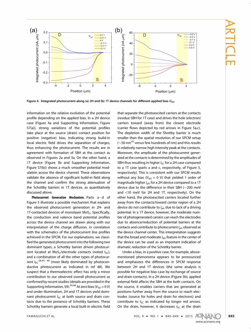
Insights into Potential Profile across Devices. Comple-mentary qualitative analysis of the Schottky barrierswas obtained by plotting the integrated photocurrentalong the devices channels (Figure 4a,b derived fromFigure 2a, including that of part c, respectively; see alsothe Supporting Information, Figure S7), that providesinsight into potential profile of 2H and 1T devices.Although this method does not provide direct accessto the intrinsic potential profile across the deviceas suggested in ref 45, it offers useful qualitative
Figure 3. (a, b) Photocurrent amplitude versus applied bias VSD at signature points of the profiles in Figure 2a (2H-) andFigure 2c (1T-contacted device), respectively. Gray regions encompass the VSD range, which corresponds to Schottky barriersheights at the source and drain.
ARTIC
LE
YAMAGUCHI ET AL. VOL. 9 ’ NO. 1 ’ 840–849 ’ 2015
www.acsnano.org
845
information on the relative evolution of the potentialprofile depending on the applied bias. In a 2H devicecase (Figure 4a and Supporting Information, FigureS7(a)), strong variations of the potential profilestake place at the source (drain) contact position forpositive (negative) bias, indicating strong build-inlocal electric field drives the separation of charges,thus enhancing the photocurrent. The results are inagreement with formation of SBH at the contact asobserved in Figures 2a and 3a. On the other hand, a1T device (Figure 3b and Supporting Information,Figure S7(b)) shows a much smoother potential mod-ulation across the device channel. These observationsvalidate the absence of significant build-in field alongthe channel and confirm the strong attenuation ofthe Schottky barriers in 1T devices, as quantitativelydiscussed above.
Photocurrent Generation Mechanism. Parts a�d ofFigure 5 illustrate a possible mechanism that explainsthe observed photocurrent generation in 2H- and1T-contacted devices of monolayer MoS2. Specifically,the conduction and valence band potential profilesacross the device channel are drawn along with ourinterpretation of the charge diffusion, in correlationwith the schematics of the photocurrent line profilesachieved in the SPCM. For our explanations, we classi-fied the generated photocurrent into the following twodominant types; a Schottky barrier driven photocur-rent located at MoS2/electrode contacts (noted ISC),and a combination of all the other types of photocur-rent IPC
38,45�48 (most likely dominated by photocon-ductive photocurrent as indicated in ref 48). Wesuspect that a thermoelectric effect has only a minorcontribution to our observed overall photocurrent asconfirmed by recent studies (details are provided in theSupporting Information, S9).39,48 At zero bias (VSD = 0 V)and under illumination, 2H and 1T devices yield domi-nant photocurrent ISC at both source and drain con-tacts due to the presence of Schottky barriers. TheseSchottky barriers generate a local built-in electric field
that separate the photoexcited carriers at the contacts(residue SBH for 1T case) and drives the hole (electron)carriers toward (away from) the closest electrode(carrier flows depicted by red arrows in Figure 5a,c).The depletion width of the Shottky barrier is muchsmaller than the spatial resolution of our SPCM setup(∼50 nm45 versus few hundreds of nm) and this resultsin relatively narrow high intensity peak at the contacts.Moreover, the amplitude of the photocurrent gener-ated at the contacts is determined by the amplitudes ofSBH thus resulting in higher ISC for a 2H case comparedto a 1T case (parts a and c, respectively, of Figure 5,respectively). This is consistent with our SPCM resultswithout any bias (VSD = 0 V) that yielded 1 order ofmagnitude higher Iph for a 2H device compared to a 1Tdevice due to the difference in their SBH (∼200 meVand <10 meV for 2H and 1T, respectively). On theother hand, the photoexcited carriers located furtheraway from the contacts/toward center region of a 2Hdevice do not contribute to Iph due to lack of a drivingpotential. In a 1T device, however, the moderate num-ber of photogenerated carriers can reach the electrodesdue to absence/reduction of potential barriers at thecontacts and contribute to photocurrent Iph observed atthe device channel center. This interpretation suggeststhat the broad andmoderate Iph feature in the center ofthe device can be used as an important indication ofdramatic reduction of the Schottky barrier.
Under a bias, in a positive case, for example, above-mentioned phenomena appears to be pronouncedand emphasizes the differences in SPCM responsebetween 2H and 1T devices (the same analysis ispossible for negative bias case by exchange of sourceand drain contacts). In a 2H device (Figure 5b), appliedexternal field affects the SBH at the both contacts. Onthe source, it enables carriers that are generated atpositions further away from the source to reach elec-trodes (source for holes and drain for electrons) andcontribute to ISC as indicated by longer red arrows.On the drain, however, it decreases ISC at the drain
Figure 4. Integrated photocurrent along (a) 2H and (b) 1T device channels for different applied bias VSD.
ARTIC
LE

YAMAGUCHI ET AL. VOL. 9 ’ NO. 1 ’ 840–849 ’ 2015
www.acsnano.org
846
contact in relative to the source due to decreased SBH(indicated by shorter arrows). Positions of high ISCregions remain unchanged. It should be noted thatthis analysis is valid in a bias range that is away from thesaturation regime of the device, and 0.5 V used in ourcase is well below the critical voltage.23 In 1T devices,the elimination effect of Schottky barriers becomesevenmore apparent upon applying an extremely smallbias of fewmillivolts (Figure 5d). The tilt/bending of theband potential rapidly enable photoexcited carriers toovercome the SBH at both contacts and render ISCnegligible (the peaks located at the contacts dis-appear). This allows for uninhibited flowof photoexcitedcarriers even under very small external electric-fieldsunlike in the case of 2H-contacted devices. As a result,IPC maximized near the center of the channel emergesand spans over the entire device. This would not bepossible with 2H-contacted device because a forma-tion of Schottky barriers at the electrodes hinderselectrons from reaching the electrodes, resulting in no
observable total photocurrent Iph (Figure 5b). The gatedependence of SPCM results is expected to providefurther insights into the evolution of Schottky barrierheights and detailed photogeneration mechanism inMoS2 based devices, and should be investigated infuture works.
Device Performance. Integrated photocurrent re-sponse along device channels (Figure 6a) and thelocal photoresponsivity (Figure 6b) demonstrate theenhanced performances of 1T-contacted devices incomparison to their 2H counterparts. We observe sametrends in the integrated photocurrent and dark currentvariations as a function of the bias (Figure 2a) as wellas comparable ratio of current amplitudes betweenthe 2H and 1T devices (about 1 order of magnitudedifference). This is consistent with the trend of 133%carrier mobility increase observed for 1T device FETs inour previous reports.22,23 Moreover, a 1T device pre-sents photoresponsivity R (ratio of the local Iph to theexcitation power) about 30 times larger (R = 5.5 mA/W)
Figure 5. Proposed mechanisms of photocurrent generation in (a, b) 2H-contacted and (c, d) 1T-contacted devices. Toppanels (a), (c) and bottom ones (b), (d) correspond to situations at zero and positive bias, respectively. In each panel, the topschematic illustrates the conduction (blue) and valence (green) bands variations along the device channel; the MoS2monolayer is sandwiched between the two metal electrodes (positions of the electrodes are shown in yellow, with S and Dcorresponding to the source and drain, respectively). Insets illustrated enlarged MoS2/electrode contact and depict theSchottky barrier height derived from our SPCM measurements. Diffusion of electrons (�) and holes (þ) are represented byred arrows, and the corresponding plot schematics for relative photocurrent versus the position along the channel areillustrated below. The direction and relative amplitude of currents are indicated by arrows in-between the two schemes,with ISC indicating the photocurrent generated by the Schottky barriers and IPC indicating photocurrent, which is a sum of all theother types.
ARTIC
LE

YAMAGUCHI ET AL. VOL. 9 ’ NO. 1 ’ 840–849 ’ 2015
www.acsnano.org
847
than a 2H device case (R = 0.2 mA/W) at VSD =�0.5 V. A2H device responsivity is almost invariant over the wholeVSD bias rangeof�0.5 to 0.5 V, in agreementwith the factthat ISC (Schottky barriers driven photocurrent) domi-nates the photoresponse. On the contrary, a 1T deviceshows strong responsivity variations in a V-shape cen-tered at VSD ≈ 0, where R presents a drastic increase asVSD overcome the SBH (photocurrent regime changesfrom ISC at low bias (�10 mVe VSDe 10 mV) to IPC). TheresponsivityR=6.3mA/WatVSD=0.5 V (excitationpower0.7 μW at 2.8 eV (440 nm)) is larger than observations inmonolayer graphene transistors47 and comparable torecent reports in monolayer MoS2 under similar opera-tion parameters.48�50 We expect further enhancementwith illumination at the excitonic absorption states.5 Ourresults demonstrate effectiveness of using the phaseengineering approach (conversion of 2H- to 1T-phase)for monolayer MoS2 to eliminate the Schottky barriers atthe contacts, thus improving the operating current levelas well as increasing the net active area of the devicethroughout the entire channel to achieve high perfor-mance 2D optoelectronic devices.
CONCLUSION
In conclusion, we performed SPCM on monolayerMoS2 individual sheet devices with phase-engineered
contacts and compared the results with conven-tionally used 2H-contacted devices. The resultsrevealed that in addition to the increased photo-current level, the active area of monolayer MoS2optoelectronic devices broadened over their entirearea due to Schottky barrier elimination of a 1Tdevice. This is in stark contrast to narrow activeregions near the electrodes for a 2H device. Further-more, analysis of SPCM results indicated that theSchottky barrier heights (SBH) at the contacts of a 1Tdevice is reduced by at least 1 order of magnitudecompared to a 2H case, from∼200meV down to fewmeV or even lower. Our proposed model suggeststhat this elimination of Schottky barriers at theelectrodes achieved by the conversion of semicon-ducting 2H-phase to metallic 1T-phase is responsi-ble for the observed broadening of the active areaand increase of photocurrent level. We also demon-strated that the photoresponsivity increases bymore than an order of magnitude for a 1T devicecompared to a 2H case, a promising indicationtoward high performance optoelectronic devices.Our results pave a pathway for the design of highperformance TMD-based 2D optoelectronic devicesand fundamental understanding of their optoelec-tronic properties.
METHODSFabrication Procedures of 1T- and 2H-Phase Contacted MoS2 Devices.
Monolayer CVD MoS2 sheets40 were transferred51 onto degen-
erately p-doped (R < 0.0015Ω-cm) patterned silicon substratescapped with 100 nm oxide layer. Statically dispensed PMMA(A4, Microchem Corp.) was spin coated onto the sample at4000 rpm for 60 s and was followed by prebaking at 180 �C for90 s. For fabrications of 1T-phase contact devices, two separatelithography processes were performed. In the first lithographystep, electrode windows were opened on the MoS2 sheet usingconventional e-beam lithography. After opening the electrodewindows, we exposed the samples to n-butyllithium (1.6M,Sigma-Aldrich) for 48 h and then cleaned themwith hexane.22,23
All butyllithium exposure was conducted in an argon-filledglovebox. Samples were then cleaned with deionized water inorder to remove residual lithium on MoS2. This was followed byPMMA etching using HPLC grade acetone (Fisher Scientific),followed by a 2-propanol rinse. PMMA was again spin coatedfollowing the same recipe as described earlier. A secondlithography stepwas performed to open the electrodewindowsat the same regions as described earlier.
We performed e-beam evaporation to deposit titanium(5 nm) and gold (50 nm) under high vacuum conditions of10�7 Torr at a slow deposition rate of 1 Å/s. This was followed bylift off using acetone after which the samples were properlyrinsed with 2-propanol to eliminate acetone residue followed
Figure 6. 2H- vs 1T-contacted devices performances and their evolution with applied source-drain bias VSD. (a) Totalphotocurrent integrated over the channel length of 2H (black dots, right scale) and 1T (red squares, left scale) devices. (b) Localphotoresponsivity extracted from the SPCM measurements as the ratio of maximum photocurrent to the excitation power.
ARTIC
LE

YAMAGUCHI ET AL. VOL. 9 ’ NO. 1 ’ 840–849 ’ 2015
www.acsnano.org
848
by blow drying with compressed nitrogen gas. For fabricationsof conventional 2H-phase contact devices, metal electrodeswere deposited without n-butyllithium exposure steps.
Scanning Photocurrent Microscopy (SPCM) and Photoluminescence (PL)Measurements. For SPCM measurements, 440 nm pulsed excita-tion light was delivered by a laser diode (PicoQuant) andfocused on the sample by a 60� Olympus objective with0.9 numerical aperture to be scanned over the samples in aform of map/line/fixed position by means of a galvanometermirror positioning system and two lenses arranged in a 4f-configuration.34 As illustrated in Figure 1a, synchronous detec-tion was achieved via SR-830 lock-in amplifier (Stanford Re-search Systems) using the reference frequency input from thechopper (∼370 Hz). The photocurrent signal was first amplifiedby a SR-570 current amplifier (Stanford Research Systems), andthe AC component of the output voltage signal was used asdirect input to the lock-in amplifier. Both the amplitude R andthe phase j of the photocurrent were monitored and analyzed.Correlated PL and/or reflected light obtained for the sameposition of SPCMmap was detected using an avalanche photo-diode and a silicon photodiode, respectively, allowing determi-nation of the exact location of monolayer MoS2 sheet devicesand the contact electrodes.
Conflict of Interest: The authors declare no competingfinancial interest.
Acknowledgment. We acknowledge S. E. Yalcin of LosAlamos National Laboratory (LANL) for the technical supportand J. A. Garcia of LANL for the administrative support at theinitial stage of SPCM system setup. We also acknowledge J. K.Baldwin of LANL for metal electrode depositions, D. J. William ofLANL for maintenance of the SEM system for e-beam lithogra-phy, and W. Nie of LANL for fruitful discussions. H.Y. acknowl-edges financial support from a LANL Director's PostdoctoralFellowship and S. K. Doorn of LANL for initial support as a host.This work was financially supported by the LANL LaboratoryDirected Research and Development (LDRD) program and wasperformed, in part, at the Center for Integrated Nanotechnolo-gies, an Office of Science User Facility operated for the U.S.Department of Energy (DOE) Office of Science by Los AlamosNational Laboratory (Contract No. DE-AC52-06NA25396) andSandiaNational Laboratories (ContractNo. DE-AC04-94AL85000).
Supporting Information Available: Optical, reflection, and PLimages for determination of device positions, SPCM on shortchannel length devices, amplitude and phase informationextracted from SPCM maps, bias-dependent SPCM maps of a2H-contacted device, reproducibility of bias-dependent SPCMmaps of a 1T-contacted device, fixed position photocurrentmicroscopy of a 1T-contacted device, effects of illuminationintensity on SBH determinations, photocurrent integrated fromopposite direction, and thermoelectric effect contributions inphotocurrents measured in this study. This material is availablefree of charge via the Internet at http://pubs.acs.org.
REFERENCES AND NOTES1. Novoselov, K. S.; Geim, A. K.; Morozov, S. V.; Jiang, D.;
Zhang, Y.; Dubonos, S. V.; Grigorieva, I. V.; Firsov, A. A.Electric Field Effect in Atomically Thin Carbon Films.Science 2004, 306, 666–669.
2. Ohta, T.; Bostwick, A.; Seyller, T.; Horn, K.; Rotenberg, E.Controlling the Electronic Structure of Bilayer Graphene.Science 2006, 313, 951–954.
3. Novoselov, K. S.; Falko, V. I.; Colombo, L.; Gellert, P. R.;Schwab, M. G.; Kim, K. A Roadmap for Graphene. Nature2012, 490, 192–200.
4. Splendiani, A.; Sun, L.; Zhang, Y.; Li, T.; Kim, J.; Chim, C.-Y.;Galli, G.; Wang, F. Emerging Photoluminescence in Mono-layer MoS2. Nano Lett. 2010, 10, 1271–1275.
5. Mak, K. F.; Lee, C.; Hone, J.; Shan, J.; Heinz, T. F. AtomicallyThin MoS2: A New Direct-Gap Semiconductor. Phys. Rev.Lett. 2010, 105.
6. Radisavljevic, B.; Radenovic, A.; Brivio, J.; Giacometti, V.; Kis,A. Single-Layer MoS2 Transistors. Nat. Nanotechnol. 2011,6, 147–150.
7. Wang, Q. H.; Kalantar-Zadeh, K.; Kis, A.; Coleman, J. N.;Strano, M. S. Electronics and Optoelectronics of Two-Dimensional Transition Metal Dichalcogenides. Nat.Nanotechnol. 2012, 7, 699–712.
8. Nicolosi, V.; Chhowalla, M.; Kanatzidis, M. G.; Strano, M. S.;Coleman, J. N. Liquid Exfoliation of Layered Materials.Science 2013, 340.
9. Chhowalla, M.; Shin, H. S.; Eda, G.; Li, L. J.; Loh, K. P.; Zhang,H. The Chemistry of Two-Dimensional Layered TransitionMetal Dichalcogenide Nanosheets. Nat. Chem. 2013, 5,263–275.
10. Jariwala, D.; Sangwan, V. K.; Late, D. J.; Johns, J. E.; Dravid,V. P.; Marks, T. J.; Lauhon, L. J.; Hersam, M. C. Band-likeTransport in High Mobility Unencapsulated Single-LayerMoS2 Transistors. Appl. Phys. Lett. 2013, 102, 173107.
11. Jariwala, D.; Sangwan, V. K.; Lauhon, L. J.; Marks, T. J.;Hersam, M. C. Emerging Device Applications for Semicon-ducting Two-Dimensional Transition Metal Dichalcogen-ides. ACS Nano 2014, 8, 1102–1120.
12. Lei, S.; Ge, L.; Najmaei, S.; George, A.; Kappera, R.; Lou, J.;Chhowalla, M.; Yamaguchi, H.; Gupta, G.; Vajtai, R.; et al.Evolution of the Electronic Band Structure and EfficientPhoto-Detection in Atomic Layers of InSe. ACS Nano 2014,8, 1263–1272.
13. Das, S.; Chen, H.-Y.; Penumatcha, A. V.; Appenzeller, J. HighPerformance Multilayer MoS2 Transistors with ScandiumContacts. Nano Lett. 2012, 13, 100–105.
14. Liu, H.; Neal, A. T.; Ye, P. D. Channel Length Scaling of MoS2MOSFETs. ACS Nano 2012, 6, 8563–8569.
15. Liu, H.; Si, M.; Deng, Y.; Neal, A. T.; Du, Y.; Najmaei, S.; Ajayan,P. M.; Lou, J.; Ye, P. D. SwitchingMechanism in Single-LayerMolybdenumDisulfide Transistors: An Insight into CurrentFlow across Schottky Barriers. ACS Nano 2013, 8, 1031–1038.
16. Baugher, B. W. H.; Churchill, H. O. H.; Yang, Y.; Jarillo-Herrero, P. Intrinsic Electronic Transport Properties ofHigh-Quality Monolayer and Bilayer MoS2. Nano Lett.2013, 13, 4212–4216.
17. Schmidt, H.; Wang, S.; Chu, L.; Toh, M.; Kumar, R.; Zhao, W.;Castro Neto, A. H.; Martin, J.; Adam, S.; €Ozyilmaz, B.; et al.Transport Properties of Monolayer MoS2 Grown by Chemi-cal Vapor Deposition. Nano Lett. 2014, 14, 1909–1913.
18. Eda, G.; Yamaguchi, H.; Voiry, D.; Fujita, T.; Chen, M.;Chhowalla, M. Photoluminescence from Chemically Exfo-liated MoS2. Nano Lett. 2011, 11, 5111–5116.
19. Eda, G.; Fujita, T.; Yamaguchi, H.; Voiry, D.; Chen, M.;Chhowalla, M. Coherent Atomic and Electronic Hetero-structures of Single-Layer MoS2. ACS Nano 2012, 6, 7311–7317.
20. Voiry, D.; Yamaguchi, H.; Li, J. W.; Silva, R.; Alves, D. C. B.;Fujita, T.; Chen, M. W.; Asefa, T.; Shenoy, V. B.; Eda, G.; et al.Enhanced Catalytic Activity in Strained Chemically Exfo-liatedWS2Nanosheets for Hydrogen Evolution.Nat.Mater.2013, 12, 850–855.
21. Voiry, D.; Salehi, M.; Silva, R.; Fujita, T.; Chen, M.; Asefa, T.;Shenoy, V. B.; Eda, G.; Chhowalla, M. Conducting MoS2Nanosheets as Catalysts for Hydrogen Evolution Reaction.Nano Lett. 2013, 13, 6222–6227.
22. Kappera, R.; Voiry, D.; Yalcin, S. E.; Branch, B.; Gupta, G.;Mohite, A. D.; Chhowalla, M. Phase-Engineered Low-Resistance Contacts for Ultrathin MoS2 Transistors. Nat.Mater. 2014, 13, 1128–1134.
23. Kappera, R.; Voiry, D.; Yalcin, S. E.; Jen,W.; Acerce, M.; Torrel,S.; Branch, B.; Lei, S.; Chen, W.; Najmaei, S.; et al.Metallic 1TPhase Source/Drain Electrodes for Field Effect Transistorsfrom Chemical Vapor Deposited MoS2. APL Mater. 2014, 2,092516.
24. Freitag, M.; Martin, Y.; Misewich, J. A.; Martel, R.; Avouris, P.Photoconductivity of Single Carbon Nanotubes.Nano Lett.2003, 3, 1067–1071.
25. Ahn, Y.; Dunning, J.; Park, J. Scanning Photocurrent Imag-ing and Electronic Band Studies in Silicon Nanowire FieldEffect Transistors. Nano Lett. 2005, 5, 1367–1370.
26. Gu, Y.; Romankiewicz, J. P.; David, J. K.; Lensch, J. L.; Lauhon,L. J. Quantitative Measurement of the Electron and Hole
ARTIC
LE

YAMAGUCHI ET AL. VOL. 9 ’ NO. 1 ’ 840–849 ’ 2015
www.acsnano.org
849
Mobility-Lifetime Products in Semiconductor Nanowires.Nano Lett. 2006, 6, 948–952.
27. Mohite, A.; Lin, J.-T.; Sumanasekera, G.; Alphenaar, B. W.Field-Enhanced Photocurrent Spectroscopy of ExcitonicStates in Single-Wall Carbon Nanotubes. Nano Lett. 2006,6, 1369–1373.
28. Ahn, Y. H.; Tsen, A. W.; Kim, B.; Park, Y. W.; Park, J.Photocurrent Imaging of p-n Junctions in AmbipolarCarbon Nanotube Transistors. Nano Lett. 2007, 7, 3320–3323.
29. Freitag, M.; Tsang, J. C.; Bol, A.; Yuan, D.; Liu, J.; Avouris, P.Imaging of the Schottky Barriers and Charge Depletion inCarbon Nanotube Transistors. Nano Lett. 2007, 7, 2037–2042.
30. Lee, E. J. H.; Balasubramanian, K.; Dorfmüller, J.;Vogelgesang, R.; Fu, N.; Mews, A.; Burghard, M.; Kern, K.Electronic-Band-Structure Mapping of Nanotube Transis-tors by Scanning Photocurrent Microscopy. Small 2007, 3,2038–2042.
31. Mueller, T.; Xia, F.; Freitag, M.; Tsang, J.; Avouris, P. Role ofContacts in Graphene Transistors: A Scanning Photocur-rent Study. Phys. Rev. B 2009, 79, 245430.
32. Mohite, A. D.; Santos, T. S.; Moodera, J. S.; Alphenaar, B. W.Observation of the Triplet Exciton in EuS-Coated Single-Walled Nanotubes. Nat. Nanotechnol. 2009, 4, 425–429.
33. Sun, D.; Aivazian, G.; Jones, A. M.; Ross, J. S.; Yao, W.;Cobden, D.; Xu, X. Ultrafast Hot-Carrier-Dominated Photo-current in Graphene. Nat. Nanotechnol. 2012, 7, 114–118.
34. Mohite, A. D.; Perea, D. E.; Singh, S.; Dayeh, S. A.; Campbell,I. H.; Picraux, S. T.; Htoon, H. Highly Efficient ChargeSeparation and Collection across in Situ Doped AxialVLS-Grown Si Nanowire p-n Junctions. Nano Lett. 2012,12, 1965–1971.
35. Yang, Y.; Li, J.; Wu, H.; Oh, E.; Yu, D. Controlled AmbipolarDoping and Gate Voltage Dependent Carrier DiffusionLength in Lead Sulfide Nanowires. Nano Lett. 2012, 12,5890–5896.
36. Jariwala, D.; Sangwan, V. K.; Wu, C.-C.; Prabhumirashi, P. L.;Geier, M. L.; Marks, T. J.; Lauhon, L. J.; Hersam, M. C. Gate-Tunable Carbon Nanotube-MoS2 Heterojunction p-nDiode. Proc. Nat. Acad. Sci. 2013, 110, 18076–18080.
37. DeBorde, T.; Aspitarte, L.; Sharf, T.; Kevek, J. W.; Minot, E. D.Photothermoelectric Effect in Suspended Semiconduct-ing Carbon Nanotubes. ACS Nano 2013, 8, 216–221.
38. Graham, R.; Yu, D. Scanning Photocurrent Microscopy inSemiconductor Nanostructures. Mod. Phys. Lett. B 2013,27, 1330018.
39. Wu, C.-C.; Jariwala, D.; Sangwan, V. K.; Marks, T. J.; Hersam,M. C.; Lauhon, L. J. Elucidating the Photoresponse ofUltrathin MoS2 Field-Effect Transistors by Scanning Photo-current Microscopy. J. Phys. Chem. Lett. 2013, 4, 2508–2513.
40. Najmaei, S.; Liu, Z.; Zhou, W.; Zou, X. L.; Shi, G.; Lei, S. D.;Yakobson, B. I.; Idrobo, J. C.; Ajayan, P. M.; Lou, J. VapourPhaseGrowth andGrain Boundary Structure ofMolybdenumDisulphide Atomic Layers. Nat. Mater. 2013, 12, 754–759.
41. Najmaei, S.; Zou, X.; Er, D.; Li, J.; Jin, Z.; Gao, W.; Zhang, Q.;Park, S.; Ge, L.; Lei, S.; et al. J. Tailoring the PhysicalProperties of Molybdenum Disulfide Monolayers by Con-trol of Interfacial Chemistry. Nano Lett. 2014, 14, 1354–1361.
42. Garcia-Belmonte, G.; Munar, A.; Barea, E. M.; Bisquert, J.;Ugarte, I.; Pacios, R. Charge Carrier Mobility and Lifetime ofOrganic Bulk Heterojunctions Analyzed by ImpedanceSpectroscopy. Org. Electron. 2008, 9, 847–851.
43. Koster, L. J. A.; Mihailetchi, V. D.; Blom, P. W. M. BimolecularRecombination in Polymer/Fullerene Bulk HeterojunctionSolar Cells. Appl. Phys. Lett. 2006, 88, 052104.
44. Wetzelaer, G.-J. A. H.; Van der Kaap, N. J.; Koster, L. J. A.;Blom, P. W. M. Quantifying Bimolecular Recombination inOrganic Solar Cells in Steady State. Adv. Energy Mater.2013, 3, 1130–1134.
45. Fu, D.; Zou, J.; Wang, K.; Zhang, R.; Yu, D.; Wu, J. Electro-thermal Dynamics of Semiconductor Nanowires underLocal Carrier Modulation. Nano Lett. 2011, 11, 3809–3815.
46. Buscema, M.; Barkelid, M.; Zwiller, V.; van der Zant, H. S. J.;Steele, G. A.; Castellanos-Gomez, A. Large and TunablePhotothermoelectric Effect in Single-Layer MoS2. NanoLett. 2013, 13, 358–363.
47. Freitag, M.; Low, T.; Xia, F.; Avouris, P. Photoconductivity ofBiased Graphene. Nat. Photonics 2013, 7, 53–59.
48. Furchi, M. M.; Polyushkin, D. K.; Pospischil, A.; Mueller, T.Mechanisms of Photoconductivity in Atomically ThinMoS2. Nano Lett. 2014, 14, 6165–6170.
49. Yin, Z.; Li, H.; Li, H.; Jiang, L.; Shi, Y.; Sun, Y.; Lu, G.; Zhang, Q.;Chen, X.; Zhang, H. Single-Layer MoS2 Phototransistors.ACS Nano 2012, 6, 74–80.
50. Choi, W.; Cho, M. Y.; Konar, A.; Lee, J. H.; Cha, G.-B.; Hong,S. C.; Kim, S.; Kim, J.; Jena, D.; Joo, J.; et al. High-DetectivityMultilayer MoS2 Phototransistors with Spectral Responsefrom Ultraviolet to Infrared. Adv. Mater. 2012, 24, 5832–5836.
51. Reina, A.; Son, H.; Jiao, L.; Fan, B.; Dresselhaus, M. S.; Liu, Z.;Kong, J. Transferring and Identification of Single- andFew-Layer Graphene on Arbitrary Substrates. J. Phys.Chem. C 2008, 112, 17741–17744.
ARTIC
LE