Acousto Optic Modulated Stroboscopic Interferometer … Optic Modulated Stroboscopic Interferometer...
113
Acousto Optic Modulated Stroboscopic Interferometer for Comprehensive Characterization of Microstructure Murali Manohar Pai S A Thesis In The Department Of Mechanical and Industrial Engineering Presented In Partial Fulfillment of the Requirements for the Degree of Master of Applied Science (Mechanical Engineering) at Concordia University Montreal, Quebec, Canada April, 2008 © Murali Manohar Pai S, 2008
Transcript of Acousto Optic Modulated Stroboscopic Interferometer … Optic Modulated Stroboscopic Interferometer...

Acousto Optic Modulated Stroboscopic Interferometer
for Comprehensive Characterization of Microstructure
Murali Manohar Pai S
A Thesis
In
The Department
Of
Mechanical and Industrial Engineering
Presented In Partial Fulfillment of the Requirements
for the Degree of Master of Applied Science (Mechanical Engineering) at
Concordia University
Montreal, Quebec, Canada
April, 2008
© Murali Manohar Pai S, 2008
1*1 Library and Archives Canada
Published Heritage Branch
395 Wellington Street Ottawa ON K1A0N4 Canada
Bibliotheque et Archives Canada
Direction du Patrimoine de I'edition
395, rue Wellington Ottawa ON K1A0N4 Canada
Your file Votre reference ISBN: 978-0-494-40918-3 Our file Notre reference ISBN: 978-0-494-40918-3
NOTICE: The author has granted a nonexclusive license allowing Library and Archives Canada to reproduce, publish, archive, preserve, conserve, communicate to the public by telecommunication or on the Internet, loan, distribute and sell theses worldwide, for commercial or noncommercial purposes, in microform, paper, electronic and/or any other formats.
AVIS: L'auteur a accorde une licence non exclusive permettant a la Bibliotheque et Archives Canada de reproduire, publier, archiver, sauvegarder, conserver, transmettre au public par telecommunication ou par I'lnternet, prefer, distribuer et vendre des theses partout dans le monde, a des fins commerciales ou autres, sur support microforme, papier, electronique et/ou autres formats.
The author retains copyright ownership and moral rights in this thesis. Neither the thesis nor substantial extracts from it may be printed or otherwise reproduced without the author's permission.
L'auteur conserve la propriete du droit d'auteur et des droits moraux qui protege cette these. Ni la these ni des extraits substantiels de celle-ci ne doivent etre imprimes ou autrement reproduits sans son autorisation.
In compliance with the Canadian Privacy Act some supporting forms may have been removed from this thesis.
While these forms may be included in the document page count, their removal does not represent any loss of content from the thesis.
•*•
Canada
Conformement a la loi canadienne sur la protection de la vie privee, quelques formulaires secondaires ont ete enleves de cette these.
Bien que ces formulaires aient inclus dans la pagination, il n'y aura aucun contenu manquant.
T^edicnttd to MM Beloved am.m.a, appa, jayafetea, rajlletefl a^d
babral
"All truths are easy to understand once they are discovered; the point is to
discover them."
—Galileo Galilei
Italian Philosopher and Mathematician (1564-1642)
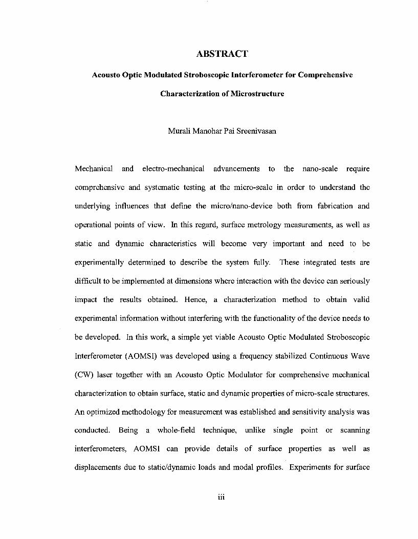
ABSTRACT
Acousto Optic Modulated Stroboscopic Interferometer for Comprehensive
Characterization of Microstructure
Murali Manohar Pai Sreenivasan
Mechanical and electro-mechanical advancements to the nano-scale require
comprehensive and systematic testing at the micro-scale in order to understand the
underlying influences that define the micro/nano-device both from fabrication and
operational points of view. In this regard, surface metrology measurements, as well as
static and dynamic characteristics will become very important and need to be
experimentally determined to describe the system fully. These integrated tests are
difficult to be implemented at dimensions where interaction with the device can seriously
impact the results obtained. Hence, a characterization method to obtain valid
experimental information without interfering with the functionality of the device needs to
be developed. In this work, a simple yet viable Acousto Optic Modulated Stroboscopic
Interferometer (AOMSI) was developed using a frequency stabilized Continuous Wave
(CW) laser together with an Acousto Optic Modulator for comprehensive mechanical
characterization to obtain surface, static and dynamic properties of micro-scale structures.
An optimized methodology for measurement was established and sensitivity analysis was
conducted. Being a whole-field technique, unlike single point or scanning
interferometers, AOMSI can provide details of surface properties as well as
displacements due to static/dynamic loads and modal profiles. Experiments for surface
i i i
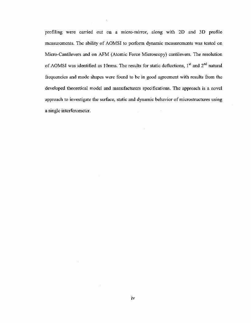
profiling were carried out on a micro-mirror, along with 2D and 3D profile
measurements. The ability of AOMSI to perform dynamic measurements was tested on
Micro-Cantilevers and on AFM (Atomic Force Microscopy) cantilevers. The resolution
of AOMSI was identified as lOnms. The results for static deflections, 1st and 2n natural
frequencies and mode shapes were found to be in good agreement with results from the
developed theoretical model and manufacturers specifications. The approach is a novel
approach to investigate the surface, static and dynamic behavior of microstructures using
a single interferometer.
iv
ACKNOWLEDGEMENT
I would like to express my sincere thanks and gratitude to my supervisors Dr.
Narayanswamy Sivakumar and Dr. Muthukumaran Packirisamy for their unwavering
encouragement. I am grateful to Dr. Sivakumar for sharing this knowledge in optical
metrology and for his support and advice to setup the Interferometer. I am also grateful to
him to show the beacon of hope with his immense knowledge during the experimental
phase. I am also very grateful to Dr. Packirisamy for sharing his knowledge on designing
of MEMS device and his feedback on the experimental setup. Their genuine enthusiasm
for this research topic created an atmosphere that was truly instrumental in the success of
this work. I would also like to thank both the supervisors who encouraged me to attend
and showcase the research in various conferences. It was a pleasure and privilege to carry
out research under them.
I Thank Dr. Petre Tzenov, Dan Juras, Charlene Wald, Arlene and other members of the
Department of Mechanical Engineering for their support and advice during the program.
A special thanks to Dr.Gino Rinaldi for his technical expertise in modeling of
microstructures. I would like to acknowledge my colleagues Ashwin, Arvind,
Raghvendra, Kiran in the Optical Microsystem Laboratory, Ramak ,Chakameh in Laser
Micromachining and Metrology Laboratory for all the support and discussions. Also I
like to acknowledge Vamshi Raghu and Rohit Singh for their emotional support for the
success of the thesis.
My parents and other members in my family deserve a warm and special
acknowledgement for their unbounded love and encouragement.
v

Table of Contents
List of Figures ix
List of Tables xii
List of Symbols xiii
Chapter 1 Introduction
1.1 Introduction 1
1.2 History of Micro Electro Mechanical Systems (MEMS) 1
1.3 Trends in Micro Electro Mechanical Systems (MEMS) 2
1.4 Factors Affecting the Growth of MEMS 4
1.5 Introduction to Characterization Tools in MEMS 6
1.6 Importance of Mechanical Characterization in MEMS 6
1.7 Classification of Characterization Tools in MEMS 7
1.8 Non-Optical Methods 7
1.9 Optical Based Method 10
1.10 Focus Sensing Techniques 10
1.11 Interferometric Techniques 12
1.12 Interferometric Techniques for Surface Profile and Static Behavior 12
1.13 Interferometric Techniques for Dynamic Characterization 13
1.14 Laser Doppler Vibrometer (LDV) 14
1.15 Whole Field Technique 16
1.16 Stroboscopic Interferometer 17
1.17 Acousto Optic Modulator (AOM) in Stroboscopy 18
vi

1.18 Working of Acousto Optic Modulator (AOM) 19
1.19 Digital Laser Microinterferometer 21
1.20 Processing Techniques on a Fringe Pattern 22
1.21 Fringe Tracking 23
1.22 Temporal Phase Measurement/Temporal Heterodyning 24
1.23 Fourier Transform 25
1.24 Objective and Scope of the Thesis 26
Chapter 2 Design and Modeling of MEMS device
2.1 Introduction 27
2.2 Rayleigh-Ritz Method 27
2.3 Energy Formulation 28
2.4 Theoretical Formulation 29
2.5 Modeling the Static Behaviour 29
2.6 Modeling the Dynamic Behaviour 33
2.7 Summary 37
Chapter 3 Experimental Setup of Acousto Optic Modulated Stroboscopic
Interferometer
3.1 Introduction 38
3.2 Basic Layout of the Interferometer 39
3.3 Systematic Design and Alignment of the Optical System 42
3.4 Fringe Analysis using Fourier Transformation 44
3.5 Sensitivity Analysis 47
3.5 Optimization of Measurement Method 51
vii

3.4 Summary 53
Chapter 4 Surface Metrology and Static Characterization
4.1 Introduction 54
4.1 Surface Metrology 54
4.2 Surface Metrology on a Connecting Pads 58
4.3 Importance of Static Characterization 59
4.4 AOMSI for Low Frequency Static Characterization 62
4.5 Measurement of Static Deflections 64
4.6 Summary 69
Chapter 5 Dynamic Characterization
5.1 Introduction 70
5.2 Dynamic Characterization 71
5.3 Identification of Natural Frequency 73
5.4 Characterization of mode shapes 75
5.5 Summary 80
Chapter 6 Conclusion
6.1 Conclusion 81
6.2 Future Work 82
References 84
Appendix
List of Journal and Conference 96
vin

List of Figures
Figure 1.1 SEM image of gyroscope 3
Figure 1.2 (a) SEM image of internal stress induced MEMS plate 5
Figure 1.3 Schematic layout of Scanning Electron Microscope [24] 8
Figure 1.4 Classifications of optical techniques 10
Figure 1.5 Full-field white light confocal microscope [25] 11
Figure 1.6 Schematic layout of Mirau interferometric technique [27] 13
Figure 1.7 Schematic layout of LDV [34] 15
Figure 1.8 Schematic of stroboscopic interferometer system [29] 17
Figure 1.9 Working regime of an Acousto Optic Modulator 20
Figure 1.10 Modulation graph of AOM [64] 20
Figure 1.11 Schematic layout of digital laser microinterferometer [41] 22
Figure 1.12 Fringe tracking method 23
Figure 1.13 Interferogram of different known phase shifts 24
Figure 2.1 Schematic of an electrostatically actuated microcantilever 28
Figure 2.2 Equivalent microcantilever with artificial springs 29
Figure 2.3 Static deflection 32
Figure 2.4 Analytical Representations of the 1st and 2nd Mode Shapes 36
Figure 3.1 Schematic overview of the principal components in AOMSI 41
Figure 3.2 Digital image of the layout of the AOMSI assembly 42
Figure 3.3 (a) Interferogram (b) Spectrum image of the interferogram 45
Figure 3.4 (a) Band-pass filter mask (b) Inverse transform image of the interferogram 46
IX
Figure 3.5 2D profile of the discontinuous image 46
Figure 3.6 2D profile of the continuous profile 47
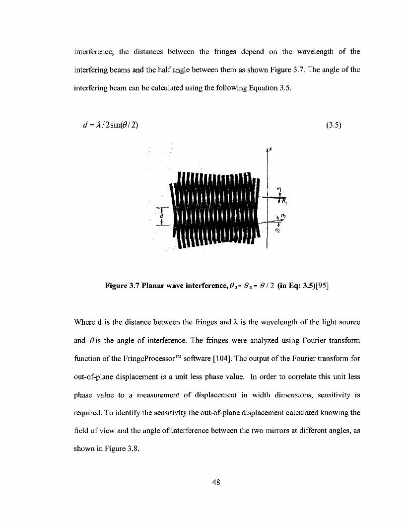
Figure 3.7 Planar wave interference 48
Figure 3.8 Angle between reference mirror and object mirror 49
Figure 3.9 Sensitivity Data of the System 51
Figure 3.10 Ra Value of the micro mirror for various number fringes 52
Figure 4.1 Torsional scanning u-mirror fabricated using MicraGeM SOI technology 55
Figure 4.2 Fringe pattern from surface of the torsional micro-mirror 56
Figure 4.3 Wrapped image after the inverse analysis of the Fourier transform method 56
Figure 4.4 2D and 3D information of the micro-mirror with the tilt information 57
Figure 4.5 2D Profile of the surface of the torsional micro-mirror 57
Figure 4.6 Surface characteristics obtained for the SOI torsional micro-mirror 58
Figure 4.7 (a) Interferogram (b) Surface information of the surface 59
Figure 4.8 Low frequency excitation using a piezo-stack 61
Figure 4.9 Methodology for static characterization of vibrating microstructures 63
Figure 4.10 Microscopic image of the micragem SOI technology cantilever 65
Figure 4.11 An SEM image of an SOI MicraGem technology cantilever array 65
Figure 4.12 Fringe patterns obtained for the DUT at various voltages 66
Figure 4.13 Static deflection comparisons 67
Figure 5.1 SEM image of the AFM cantilever 70
Figure 5.2 Methodology to conduct dynamic characterization 72
Figure 5.3 Digital image of the interferometer during dynamic characterization 75
Figure 5.4 The observed fringe pattern obtained seen on AFM cantilevers 77

Figure 5.5 Surface profile of a resonating AFM cantilever in the Is mode 78
Figure 5.6 Surface profile of a resonating AFM cantilever in the 2nd mode 79

List of Tables
Table 1.1 Comparison of non-optical characterization methods for MEMS 9
Table 1.2 Comparison of different fringe processing techniques 26
Table 2.1 Specification of the SOI MicraGem cantilever 31
Table 2.2 Theoretical tip deflection for static characterization 32
Table 2.3 Specification of AFM cantilever 35
Table 2.4 Theoretical resonance frequency 35
Table 3.1 Tabulation of number of fringes to out of plane displacement 50
Table 4.1 Tip deflection of the DUT for static characterization 68
Table 5.1 Comparison of natural frequency 74
xn

List of Symbols
cm
C
cd
Cdc
d
do
E
f
F
GPa
h
H
Hz
I
kg
kHz
kE
KE
KR
Kj"
L
Centimeter
Capacitance
Damping factor
Critical damping factor
Distance
Dielectric gap
Young's modulus of elasticity
Frequency
Geometry conditioning function
GigaPascal
Material thickness
Height
Hertz
Moment of inertia
Kilogram
Kilohertz
Electrostatic spring stiffness
Electrostatic spring stiffness
Rotational spring stiffness
Translation spring stiffness
Length
xiii
m
mm
M
MHz
nm
N
t
T
UB
UE
UED
UMAX
V
v;
v/
w
w(x)
W(x)
Ws(x)
W0
Meter
Millimeter
Mass
MegaHertz
Nanometer
Newton
Time
Temperature
Strain energy
Electrostatic potential energy
Electrostatic dynamic potential energy
Maximum potential energy
Voltage
Voltage (non-dimensionalized)
Voltage (non-dimensionalized)
Material width
Positional width
Flexural deflection
Static Deflection
Unconditional Width
x Non-dimensionalized coordinate
y Non- dimensional co-ordinate
xiv

e Coefficient of thermal dependence for Young's modulus
so Permittivity of free space
sr Relative permittivity of a given medium
<Po W Parent polynomial in x
P*^x' 1th orthogonal polynomial i n x
^j j * orthogonal polynomial in x
^' ^x* First derivative of ith orthogonal polynomial in x
Vj First derivative of j * orthogonal polynomial in x
Pi W Second derivative ofi t h orthogonal polynomial in x
f :th „ .1 1 i „ : „ i : „ „ *J
*
*K
A
jum
n
P
(x) Second derivativ
Phase Value
Eigenvalue
Wavelength
Micrometer
Pi
Material density
co Frequency
xv
Chapter 1
Introduction
1.1 Introduction
Micro Electro Mechanical Systems (MEMS) are miniaturized devices with mechanical
components with features in the range of few urn and integrated with electronic circuitry
for signal processing and analysis. The versatility of MEMS has been the driving force
for next generation sensors, actuators and transducers in recent times. The field of MEMS
as it is known in North America is also known as Micro System Technology (MST) in
Europe and as Micromachines in Japan [1]. Over the years since its implementation,
MEMS have found its application in various fields from automobile to biological sensing
and some are yet to be uncovered.
1.2 History of Micro Electro Mechanical Systems (MEMS)
The integrated circuit (IC) technology is the starting point in the history of Microsystems.
Microfabrication for these IC technologies was developed with a level of fierceness
unmatched to other fields. These microfabrication technologies were rapidly matured
over the decades from early 1960's. The field of microelectromechanical systems
(MEMS) was evolved as an off-shoot of these technologies. Several IC processing
technologies were used to make micromechanical devices that included cantilevers,
membranes and nozzles. Crucial elements like microsensor, including piezoresistivity of
silicon were discovered, studied and optimized [3,7,4]. The bulk micromachining and
1
surface micromachining technologies [9,10,12] produced sensors at low cost that
produced large impact on various products such as ink-jet printers manufactured by
Hewlett-Packard which work on silicon micromachined ink-jet printer nozzle in [14,13].
In 1989, first silicon surface micromachined micro-motor using the principle of
electrostatic force was demonstrated at University of California at Berkeley [15]. These
developments played a significant role in bringing MEMS to broader scientific
community and industries. In 1990s, MEMS grew rapidly with government and private
funding for research in various applications from optical attenuation in
telecommunication to biological studies using MEMS based miniature tools. Early
research in companies like Analog devices and Texas Instrument started to bear results
for their invention in inertia sensors and projection display. At present the trend is still on
to compose lab-on-a-chip to miniaturize analysis system in medical application. Nano
Electro-Mechanical System (NEMS) is on a threshold to make unprecedented sensitivity
and selectivity of detection [16,17,18,76,78].
1.3 Trends in Micro Electro Mechanical Systems (MEMS)
Outcome of the above mentioned applications made scientific society to create a separate
platform dedicated to research on MEMS. The developed Microfabrication and
micromachining process was customized to produce MEMS devices [79,81,82,75].
Processes developed offered significant advantages over macroscopic electro-mechanical
sensors, principally high sensitivity and low noises. Its Bulk micromachining [80]
advantage helped the sensor and other commercial application markets on a spin with
low-cost manufacturing with high sensitivity. Advance feature integration with ultra high
2

sensitivity [19,20] are been offered. Today, one can find variety of micromachined
accelerometer sensors with various sensing principles like capacitive sensing [20],
piezoresistivity, optical sensing [21] have been demonstrated.
Its multi-disciplinary application from biomedical to aerospace has made researchers
customize their approach in development of MEMS device to satisfy their needs. In the
next 10 to 20 years the MEMS research is expected to continue its rapid growth curve
with advancements in several aspects: (1) An increased functional reach of MEMS in
interdisciplinary applications; (2) the maturation of design methodology and fabrication
technology; (3) the enhancement of mechanical performances such as sensitivity and
robustness; (4) a lowered development cost and cost of ownership [78,77]. Figure 1.1
shows SEM image of a gyroscope designed by the author to sense change in angle.
Figure 1.1 SEM image of gyroscope
3

1.4 Factors Affecting the Growth of MEMS
From the talk given by Richard Feynman about "There is plenty of room at the bottom"
scientific community [16] developed a whole new area of getting miniaturized. The
factors that affect this growth are in developing new principles and theories that predict
the models in micro or nano scale [22]. The models were simulated for various
parameters and quantified. Since it is an electromechanical system the device was
characterized for electrical and mechanical properties. Scientific community always
needs a well proven feedback system to optimize their design either of the fabrication
techniques or system. This feedback system is a main factor that helps in the
advancement of further development. To create a feedback system, better characterization
tools have to be developed for understanding various properties [92,87]. Characterization
plays an important role in connecting the link between the theoretical and experimental
research [89]. It gives the actual performances of the system. It can predict the failure and
other responses which can be used in further development of the design. Figure 1.2 shows
the SEM image of internal stress induced in the MEMS design due to fabrication
technique and design compensation made to reduce the internal stress.
4

(a)
Bgg^j^ETnrsrTyJKV-ilE:: Siigft
(b)
Figure 1.2 (a) SEM image of internal stress induced MEMS plate (b) Design
compensation on the MEMS plate.
5

1.5 Introduction to Characterization Tools in MEMS
Since the scope of the thesis is within the limits of the characterization of static and
dynamic behavior of the MEMS device, attention is drawn to various tools available to
characterize mechanical behavior of the MEMS devices in their working environment.
The parameters that need to be measured are out-of-plane motion, natural frequency, in-
plane motion and modal shape analysis. Other properties that need to be characterized are
surface metrology to understand the surface roughness of the material after it is either
deposited or fabricated on to a system.
1.6 Importance of Mechanical Characterization in MEMS
Micro Electro Mechanical System (MEMS) involves integration of electronics and
mechanical systems. The factors affecting the performances of MEMS devices have
equal effect from both systems (mechanical and electronics). Therefore optimization of
mechanical system needs tools which can characterize the mechanical behavior to study
the change in sensitivity or performances with change in design of its boundary
conditions or structure. Device level metrology plays an important role in characterizing
the parameters that governs the design of these microstructures. The important
parameters are surface roughness of the microstructure that governs the optical
attenuation properties [77,78] static behavior of these microstructures under various
working environments and sensitivity of these microstructures on loads with its
maximum capability to handle these loads. In MEMS devices, loads can be applied using
external forces (thermal or pressure) or electro-static force in the system [84]. Another
important parameter to characterize is the dynamic behavior in order to understand the
6
resonance frequency of the microstructure which is usually very high compared to macro
systems and mode shapes in resonance frequency.
1.7 Classification of Characterization Tools in MEMS
The tools to characterize these microstructures are non-contact and non-destructive
methods. The ability to view and characterize these microstructures can be done either
through a microscope or other optical methods. Bosseboeuf et al [23] discuss about the
trends of many optical techniques for out-of-plane motions that are the latest trends built
using sophisticated electronic devices in order to visualize these microstructures in its
static or dynamic motion, tools available to characterize can be classified into non-optical
methods [24] and optical methods [23].
1.8 Non-Optical Methods
The most common of the non-optical methods is Scanning Electron Microscope (SEM)
[24]. From the discovery of electron to be used for imaging using electron backscattered
diffraction images, SEM [24,58] was invented. These microscopes gave a new trend in
visualization to view material in sub nanometer resolution, providing minute details of
the structure under test. The other non-optical method was using probes to give the
surface topography, where microscopes build using tunneling and magnetic principles
were employed. The various types of Non-Optical microscope are Scanning Capacitance
microscope (SCM)[90], Atomic Force Microscope (AFM) [60], Scanning Probe
Microscope (SPM), Scanning Tunneling Microscope (STM)[91], Tunneling
7
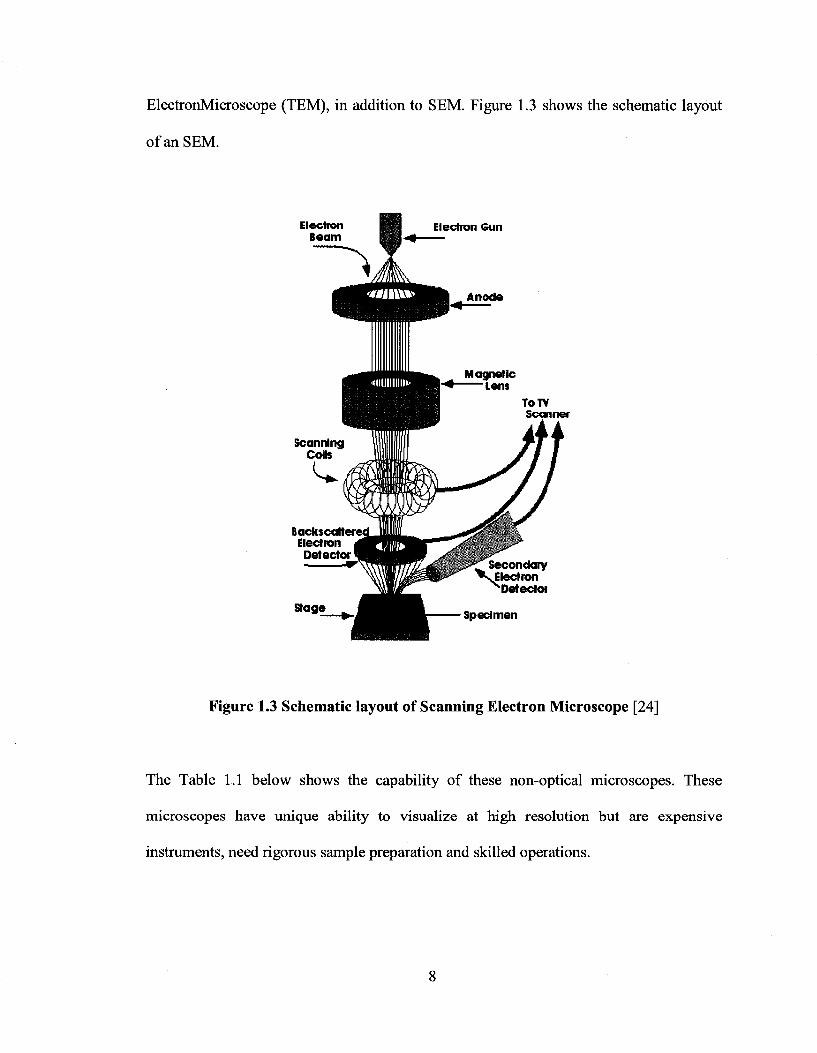
ElectronMicroscope (TEM), in addition to SEM. Figure 1.3 shows the schematic layout
ofanSEM.
Figure 1.3 Schematic layout of Scanning Electron Microscope [24]
The Table 1,1 below shows the capability of these non-optical microscopes. These
microscopes have unique ability to visualize at high resolution but are expensive
instruments, need rigorous sample preparation and skilled operations.
8

Operation
Depth of Field
Later Resolution
Vertical Resolution
Magnification
Sample
Contrast
SEM/TEM
Vacuum
Large
l-5nm-SEM
O.lnm-TEM
N/A
10X-10bX
Un-chargeable, vacuum
compatible thin fllm:TEM
Scattering, diffraction
SPM/AFM
Air, Liquid, High Vacuum
Medium
2-10nm-AFM
O.lnm-STM
0.1 nm-AFM
0.0lnm- STM
5x10²X- 10SX
Surface height < 10mm
Tunneling
Table 1.1 Comparison of non-optical characterization methods for MEMS
Moreover the non-optical approaches mentioned here are used for surface profile
measurement [58,59] but that fail to understand the static and dynamic behavior of
microstructure in real time. Optical techniques described by Bossebouef. A et al [23]
show a promising trend in developing characterization tools for static and dynamic
behavior.
9

1.9 Optical Based Method
Optical characterization techniques developed for the assessment of microstructure [42]
have promising trend to develop low-cost, high resolution, high sensitivity instruments to
conduct static and dynamic behavior of microstructure at high speed under normal
environments. The inclusion of CCD sensor and software integration with this hardware
makes the system more versatile in testing for various parameters. Optical based
characterization tools can be classified into two main categories as shown in Figure 1.4
focus sensing and interferometric techniques.
_T Focus sensing Techniques Interferometric
Techniques
Figure 1.4 Classifications of optical techniques
1.10 Focus Sensing Techniques
Optical microscope is the common focus sensing device. It magnifies the object under
test to a given order. Many principles like epifluorescence are used in characterizing
microstructures (microchannels) [93]. To be mentioned is confocal microscope which is
an important type of focus sensing technique. Its a replacement of diamond tip stylus to
an optical stylus to scan the surface profile of a microstructure or can be used for
10

understanding static behavior of microstructures in full-field [25,26]. It is one of the
most important focus sensing technique for surface profiling for structures in micro-
regime and other materials (biological and bio-medical) [107]. Gu M et al [25] proposed
a scanning system confocal microscope to record various sections of a microstructure
using CCD and then to reconstruct them in 3D profiles. Figure 1.5 shows the schematic
layout of the confocal microscope. The disc is spiral configuration of various pinholes
(Nipkow disc) helps in deleting the out-of-focus information for better imaging, a CCD
camera is used to capture the image and white light source for focusing images.
CCD Camera
Figure 1.5 Full-field white light confocal microscope [25]
While microscopes are mainly focused for 3D profile information, interferometric
techniques developed are most widely used due its capability to conduct characterization
for surface information, static and dynamic behavior.
11

1.11 Interferometric Techniques
Interferometric techniques are an extension of focus sensing technique by using the
concept of interference of light [94,95,97]. Analyzing the surface or other parameters
like motion and frequency using interferogram is the basis of an interferometric
technique. An interferogram is recorded by interference signal between two or more
beams of light exciting from the same radiation source. Interference usually refers to the
interaction of two or more light waves [95]. An interferometer is an optical setup to
create required interferences. Depending on the applications, a suitable interferometer is
used to create an interferogram. Christian Rembe et al [30] review the various trends on
optical interferometric techniques to study the dynamic behavior of the MEMS.
Bossebouf. A et al [23] also review various trends developed to study the surface
information and static behavior of MEMS devices. Some of the techniques used in
MEMS are reviewed below.
1.12 Interferometric Techniques for Surface Profile and Static Behavior
Assessment of surface profile of microstructure is important in fabrication process
optimization for designing of microstructure. Static behavior characterization gives the
information of performances of microstructure under static loads. Microscopic
interferometry are widely used for the same with most common configuration using
monochromatic or white light source such as a Michelson, Mirau or Linnik
interferometric methods. C.Quan et al [27] developed an experimental setup with Mirau
12

objective to understand the nanoscale deformation of MEMS structures. A schematic
layout of the experimental setup of the optical system is shown in Figure 1.6. The
technique was to develop a microscope with a mirau objective to obtain fringe pattern
with the structure for measurement of surface profile and static deflection.
ieiMbuife,.-
' "j? • diaphragm I . » 2 I on. 1 r
1 Humiliation system
Adjustable »<*e 'M'fcpiiKw (V
Figure 1.6 Schematic layout of Mirau interferometric technique [27]
The system developed showed the feasibility to understand the 3D deformation and
surface contour measurements for microstructures, but unable to perform dynamic
characterization.
1.13 Interferometric Techniques for Dynamic Characterization
Dynamic characterization of microstructure leads to measurement of dynamic properties
of microstructure while it is vibrating and modal analysis of the microstructure at high
frequencies. Advances in optical methodology to develop tools to measure microstructure
13
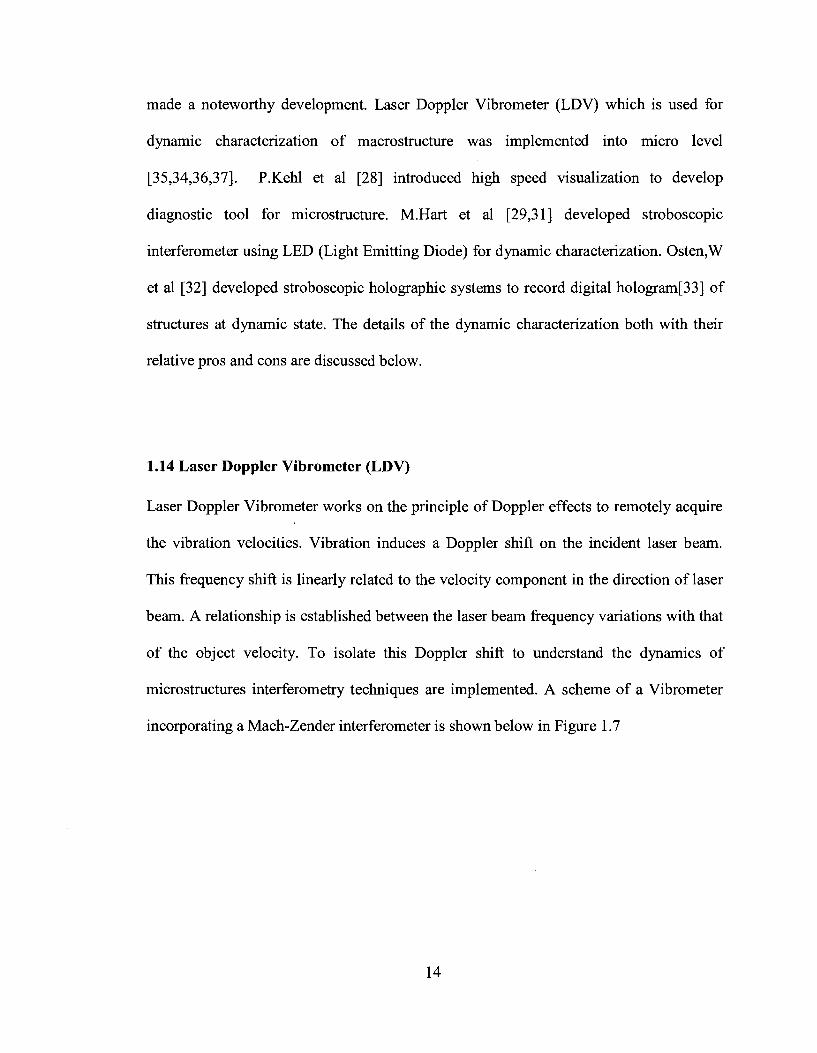
made a noteworthy development. Laser Doppler Vibrometer (LDV) which is used for
dynamic characterization of macrostructure was implemented into micro level
[35,34,36,37]. P.Kehl et al [28] introduced high speed visualization to develop
diagnostic tool for microstructure. M.Hart et al [29,31] developed stroboscopic
interferometer using LED (Light Emitting Diode) for dynamic characterization. Osten,W
et al [32] developed stroboscopic holographic systems to record digital hologram[33] of
structures at dynamic state. The details of the dynamic characterization both with their
relative pros and cons are discussed below.
1.14 Laser Doppler Vibrometer (LDV)
Laser Doppler Vibrometer works on the principle of Doppler effects to remotely acquire
the vibration velocities. Vibration induces a Doppler shift on the incident laser beam.
This frequency shift is linearly related to the velocity component in the direction of laser
beam. A relationship is established between the laser beam frequency variations with that
of the object velocity. To isolate this Doppler shift to understand the dynamics of
microstructures interferometry techniques are implemented. A scheme of a Vibrometer
incorporating a Mach-Zender interferometer is shown below in Figure 1.7
14
Object bemn
\
Itaiitpl* %ifcr»ttaa
R*f#i*uc# back ««tl«tMl beam
Mirror Bragg «*•
Mixed (inteiferiniO
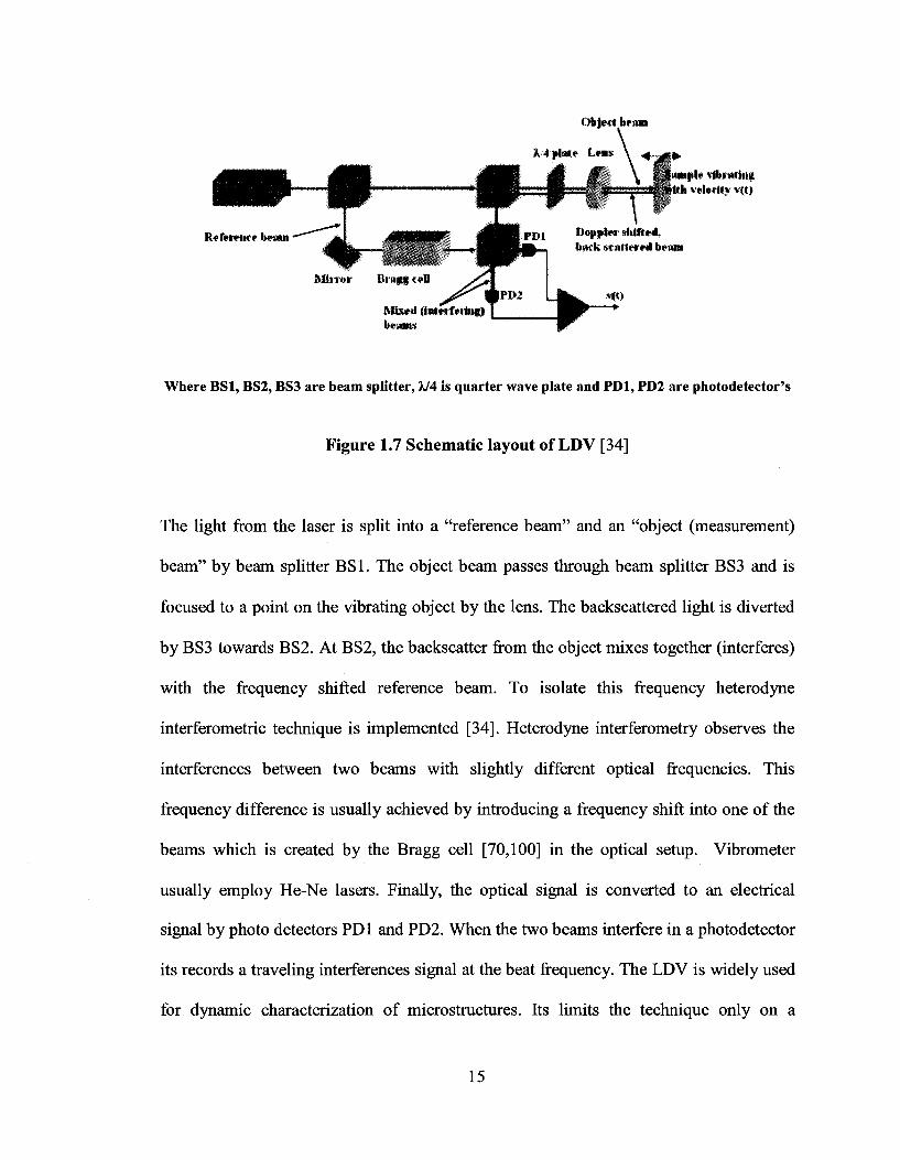
Where BS1, BS2, BS3 are beam splitter, X/4 is quarter wave plate and PD1, PD2 are photodetector's
Figure 1.7 Schematic layout of LDV [34]
The light from the laser is split into a "reference beam" and an "object (measurement)
beam" by beam splitter BS1. The object beam passes through beam splitter BS3 and is
focused to a point on the vibrating object by the lens. The backscattered light is diverted
by BS3 towards BS2. At BS2, the backscatter from the object mixes together (interferes)
with the frequency shifted reference beam. To isolate this frequency heterodyne
interferometric technique is implemented [34]. Heterodyne interferometry observes the
interferences between two beams with slightly different optical frequencies. This
frequency difference is usually achieved by introducing a frequency shift into one of the
beams which is created by the Bragg cell [70,100] in the optical setup. Vibrometer
usually employ He-Ne lasers. Finally, the optical signal is converted to an electrical
signal by photo detectors PD1 and PD2. When the two beams interfere in a photodetector
its records a traveling interferences signal at the beat frequency. The LDV is widely used
for dynamic characterization of microstructures. Its limits the technique only on a
15

vibrating body, which makes it not viable for surface profile or static characterization.
One of the first commercial dynamic characterization tools was developed based on LDV
by Polytec™ Inc. In the latest product it has a capability to detect up to 20MHz signal
with scanning system to predict more precisely the dynamic property of a whole device
[71,72]. Since LDV is either single point system [37] or scanning system [34,73] it
removes the real time assessment [38, 29] and does not have a method to visualize the
motion at higher frequency. Being a single point measurement, the position of the laser
beam along the device can also misdirect the results (eg: at nodal point in second or
higher mode analysis).To visualize these motion and to extract dynamic parameters of the
whole device in real-time, whole -field approach would be a better solution [101].
1.15 Whole Field Technique
There is a need for a static and dynamic characterization tool which can visualize the
whole system. Opting for non-optical system is expensive and time intense. An optical
system with Doppler principle can be reliable but it is either point or scanning method for
testing and cannot be used for static behaviors and it is not a whole field technique. The
implementation of interferometric technique with a suitable interferometer to measure the
phase of whole system is feasible. To make it compatible for dynamic behavior we can
use the principle of stroboscopic imaging [39,40]
16

1.16 Stroboscopic Interferometer
Stroboscopy is an alternative method [62,63] for high speed visualization[98] of cyclic
motions. Instead of using an expensive high-speed CCD camera to capture the motion of
vibrating body, the light is pulsed at the same frequency at which the object is vibrating.
In this method a normal 30 Hz CCD camera is sufficient to capture these motions.
C.Rembe et al [40] developed a stroboscopic interferometer at BASC (Berkeley Sensor&
Actuator Center) to measure in-plane and out-of-plane displacement in a single
experiment. The motion was measured with out-of-plane resolution in the order of 5nm.
The setup had capability to strobe laser at 1 MHz. Figure 1.8 is the schematic layout of
the stroboscopic interferometer developed at BASC [29].
G lass fiber
-»- GPIB I I | ° £V£
Where L - X/2 -wave-plate, P - polarizer, PBS - polarization beam splitter, fc- condenser lens, f| -imaging lens, and fm - microscope objective for imaging, LD - laser diode, M - reference mirror
F i g u r e 1.8 Schemat i c of s t roboscopic i n t e r f e rome te r sys tem [29]
The interferometer was built on using LED as a source on a Twyman-Green
interferometer [102] platform with a CCD camera connected to a frame grabber card. The
17
pulsing and the driving frequencies of the microstructure were controlled using a
computer and the capturing of the motion was done using software. The post processing
of the interferogram was done using phase-shifting method. In phase shifting method
there is a need to capture images of the same motion at different phases. Even though a
better resolution is obtained using this method it complicates the system. Moreover PZT
based phase shifting induces mechanical errors which is compensated by algorithms. The
strobing is done using a pulse generator on a LED whose reliability fails at higher
frequencies. Moreover LEDs are not monochromatic and have restrictions in coherence
length and frequency stability. Use of Acousto-Optic Modulator is feasible to get a He-
Ne laser source to strobe. He-Ne laser are monochromatic of light at 632.8 nm, unlike
LED they are frequency stabilized which is important for high precision metrology
[64,99].
1.17 Acousto Optic Modulator (AOM) in Stroboscopy
The laser system that emits continuous wave of monochromatic light are not expensive
and comes in lower power ranges is best suited for interferometric process [42]. To strobe
continuous wave laser, shutters are required. Common methods of strobing include
mechanical/electronic shutters that are good at lower frequencies. The electronic shutters
available are in few KHz ranges [108]. At higher frequencies there are LED modules.
The dynamic range on MEMS device is between few KHz to few MHz. Alternative
methods with ability to strobe at higher frequencies is necessary. AOM is widely used for
modulation in telecommunication [68], in heterodyne interferometers (Bragg cell) for
frequency variation and acoustic switching on high power pulsed laser [53], non-
18
mechanical scanning [38]. AOM with low random access time can be used for strobing a
laser in high frequency range.
1.18 Working of Acousto Optic Modulator (AOM)
The modulation in an Acousto Optic Modulator is based on the elasto-optic effect, where
the change in refractive index of the material is based on the strain. With acoustic waves
having sinusoidal properties there is grating effect caused on the crystal which diffracts
the light at various orders [65]. A parameter is called the "quality factor, Q", determines
the interaction regime. Q is given by
27rA L Q = —— ( l . i)
«A
where X is the wavelength of the laser beam, n is the refractive index of the crystal, L is
the distance the laser beam travels through the acoustic wave and A is the acoustic
wavelength.
For Q«\ : This is the Raman-Nath regime. The laser beam is incident roughly normal
to the acoustic beam and there are several diffraction orders as shown in Figure 1.9. For
Q»\ : This is the Bragg regime. At one particular incidence angle&B, only one
diffraction order is produced the others are annihilated by destructive interference as
shown is Figure 1.9. Where &B is defined by
0B = sin-.r^i 0.2)
19
Where F is acoustic frequency and v is the acoustic velocity and X is the wavelength of
the laser [69,65,64].
Raman Regime
1" Order
Bragg Regime
Zero Order
Figure 1.9 Working regime of an Acousto-Optic Modulator
R I S E T I M E ( N A N O S E C O N D S )
1 0 0 75
50 4 0
I B
7 . 5 *<~ ^s /
rt*-* ^ ^ <s JJ,
.««* ^
^ ' ^ S*
*r* x >
i**
3 d B B a n d w i d t h ( M H z )
1.2
7.0 8.7S
35 .0 4 7 . 0
400 ©00 800 12SO 2O0O 1000 1500
1 /e S p o t S i z e ( m i c r o n s ) M o d u l a t o r P e r f o r m a n c e
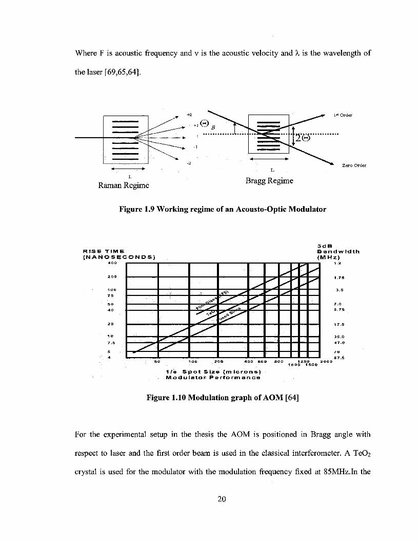
Figure 1.10 Modulation graph of AOM [64]
For the experimental setup in the thesis the AOM is positioned in Bragg angle with
respect to laser and the first order beam is used in the classical interferometer. A TeC>2
crystal is used for the modulator with the modulation frequency fixed at 85MHz.In the
20

experiment 632.8 nm laser is converted from continues wave (CW) to pulsed wave using
AOM in combination with a TTL signal generator. The beam size of the laser is 500 urn
which is given as the input to the AOM, as per the graph in Figure 1.10 a maximum
modulation capacity of 4 MHz for the given beam size is expected. With the decrease of
the beam diameter in the input side of AOM a modulation of up to 70 MHz can be
achieved [64]. The principle of AOM to strobe the light was implemented in digital laser
microinterferometer which is discussed further.
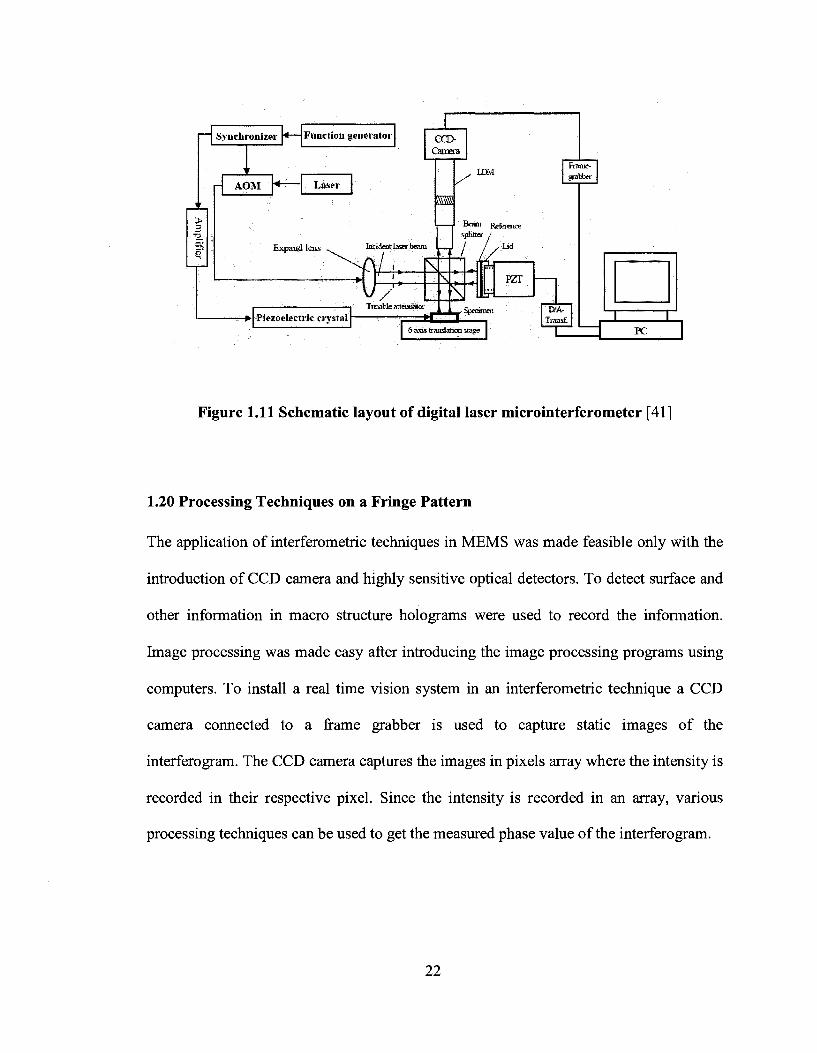
1.19 Digital Laser Microinterferometer
L.Yang et al[41] developed a digital laser microinterferometer using AOM to strobe the
laser, together with a Michelson interferometer to implement an electronic speckle
pattern interferometry. Speckle interferometry uses the speckle patterns to get the
information of the test object. It can record the displacement by co relating these speckle
patterns after a force is applied. Speckles are well defined on rough surface and
displacement measurement can be more precise, if the speckles are well defined. Figure
1.11 below shows the schematic layout of digital laser microinterferometer based on
speckle interferometry. The drawback of this system is that it needs a surface suitable to
create a speckle pattern. Most of the MEMS device surfaces are made of either metals or
silicon which reflects light. Primary requirement of speckle is to have rough surface
where the surface instead of reflecting, scatters the light to form local interferences to
create speckles. Thus it limits its range of usability in MEMS field.
21
Synchronizer f*—Function generator ca> Camera
H AOM Laser
Expand leas
^
Iocidcaf laser beam
Mm
Piezoelectric crystal Tunable att«iua»a'
K
LEW
B*™1 Refaaiw splitter
Lid U 1/ pzr
6-asis traasiatian stage
Frame-grabber
Df'A-Ttm&t
PC
Figure 1.11 Schematic layout of digital laser microinterferometer [41]
1.20 Processing Techniques on a Fringe Pattern
The application of interferometric techniques in MEMS was made feasible only with the
introduction of CCD camera and highly sensitive optical detectors. To detect surface and
other information in macro structure holograms were used to record the information.
Image processing was made easy after introducing the image processing programs using
computers. To install a real time vision system in an interferometric technique a CCD
camera connected to a frame grabber is used to capture static images of the
interferogram. The CCD camera captures the images in pixels array where the intensity is
recorded in their respective pixel. Since the intensity is recorded in an array, various
processing techniques can be used to get the measured phase value of the interferogram.
22
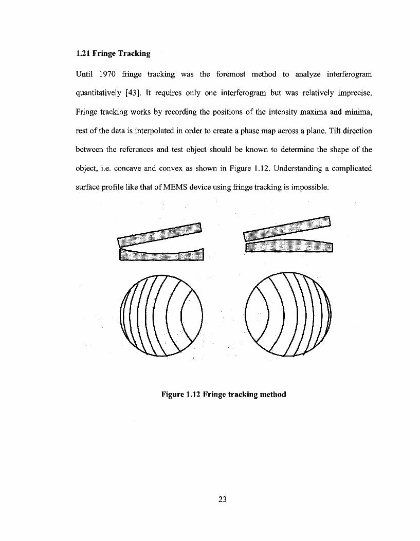
1.21 Fringe Tracking
Until 1970 fringe tracking was the foremost method to analyze interferogram
quantitatively [43]. It requires only one interferogram but was relatively imprecise.
Fringe tracking works by recording the positions of the intensity maxima and minima,
rest of the data is interpolated in order to create a phase map across a plane. Tilt direction
between the references and test object should be known to determine the shape of the
object, i.e. concave and convex as shown in Figure 1.12. Understanding a complicated
surface profile like that of MEMS device using fringe tracking is impossible.
r 1
Figure 1.12 Fringe tracking method
23
1.22 Temporal Phase Measurement/Temporal Heterodyning
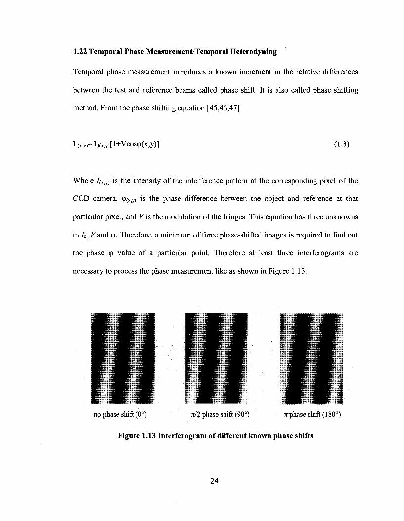
Temporal phase measurement introduces a known increment in the relative differences
between the test and reference beams called phase shift. It is also called phase shifting
method. From the phase shifting equation [45,46,47]
I (x,y)= I()(x,y)[l+VC0S(p(x,y)] (1.3)
Where 7(X;y) is the intensity of the interference pattern at the corresponding pixel of the
CCD camera, (p(x,y) is the phase difference between the object and reference at that
particular pixel, and Fis the modulation of the fringes. This equation has three unknowns
in IQ, Fand (p. Therefore, a minimum of three phase-shifted images is required to find out
the phase cp value of a particular point. Therefore at least three interferograms are
necessary to process the phase measurement like as shown in Figure 1.13.
no phase shift (0°) nil phase shift (90°) n phase shift (180°)
Figure 1.13 Interferogram of different known phase shifts
24

The most common way to shift the phase is by changing the reference mirror in the
optical axis. It is made possible by mounting the mirror on piezo stage which moves the
mirror in nanometers. The measurement precision can be improved using more samples
and using better algorithms [46,63]. The measurement can be precise with nanometer
resolution with high repeatability. But temporal phase shifting methods are not most
suitable for dynamic characterization. The setup to capture three or more interferograms
instantaneously (also referred as spatial phase shifting) is possible only with multiple
cameras, where alignment of cameras with pixel to pixel accuracy is complicated.
1.23 Fourier Transform
Fourier transform technique discretizes a single interferogram into three distinist spectral
orders for a cosinusoidial function that represents the fringes. The number of fringes from
the induced tilt between the references and test wavefront must be large enough to
separate the spectral orders to enable filtering at the spatial frequency of the fringes.
Inverse transform is then performed to phase encode the interferogram from arctangent
function of the real and imaginary parts of the inverse transform [48,49]. A phase
measurement from Fourier transform is more precise than fringe tracking but less than
phase shifting. Its algorithms are much simpler and fast to process. Better filter to remove
spatial noise improves the measurements [44]. The advantage of using Fourier transform
over phase shifting (Temporal Phase measurement) and fringe tracking is given in Table
1.2 below.
25

Parameters
Number of Interferograms
Resolution
Experimental effort
Sensitivity to external
influences
Cost
Fringe
Tracking
1
1 to 1/10 I
Low
Low
Low
Phase Shifting
Minimum 3
1/10 to 1/100 X,
High
Moderate
High
Fourier Transform
1
1/10 to 1/30 X
Moderate
Low
Moderate
Table 1.2 Comparison of different fringe processing techniques
1.24 Objective and Scope of the Thesis
The primary objective of this research work is to develop a simple yet viable stroboscopic
interferometer with a CW laser for comprehensive mechanical characterization of
microstructures. The scope of the thesis includes
• Modeling and design of simple MEMS microstructures to study static and
dynamic behaviors using the Raleigh-Ritz method.
• Designing and building Acousto Optic Modulated Stroboscopic Interferometer
(AOMSI).
• Conduct experiments on various microstructures to characterize their surface,
static, dynamic behavior.
• Comparing the experimental results with that of theoretical models to validate the
design of the interferometer.
26

Chapter 2
Design and Modeling of MEMS device
2.1 Introduction
In microsystems, theoretical modeling and simulations play a vital role. Theoretical
modeling [74,89] of MEMS devices involves understanding the microstructure when it is
subjected to various electrostatic loads and boundary conditions. The modeling is done in
order to understand the properties to predict their static and dynamic behaviors under
different influences. For example, when these microstructures are activated with an
electrostatic field, the structure deflects under the applied voltage. Similarly when the
microstructure is made to vibrate, it resonates at a particular natural frequency to take the
shape of the vibration mode. In our dynamic modeling natural frequency of the device
and also the mode shape is simulated to understand the dynamic behavior.
2.2 Rayleigh-Ritz Method
Fundamental Frequency is of greatest interest when it comes to the analysis of vibration
in a mechanical system. Rayleigh-Ritz improved the method with introduction of a series
of the shape function multiplied by a constant co-efficient. The equation resolves to give
better solution for natural frequency and mode shapes when a satisfying shape function is
used for the geometric boundary conditions [50]. In the analysis for both static and
dynamic behavior of the MEMS device the Rayleigh-Ritz energy method is used. In the
27
dynamic analysis of the cantilever the boundary characteristic orthogonal polynomials
were employed and the same is adopted for the static deflection.
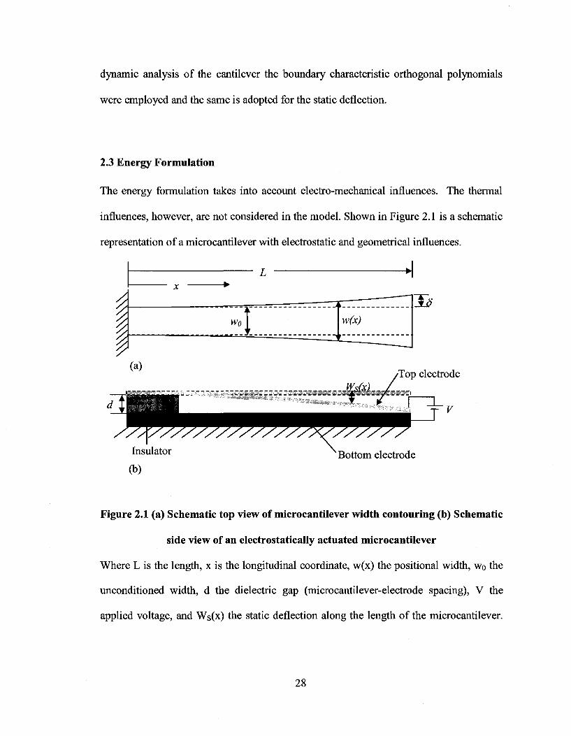
2.3 Energy Formulation
The energy formulation takes into account electro-mechanical influences. The thermal
influences, however, are not considered in the model. Shown in Figure 2.1 is a schematic
representation of a microcantilever with electrostatic and geometrical influences.
Top electrode
Bottom electrode
Figure 2.1 (a) Schematic top view of microcantilever width contouring (b) Schematic
side view of an electrostatically actuated microcantilever
Where L is the length, x is the longitudinal coordinate, w(x) the positional width, wo the
unconditioned width, d the dielectric gap (microcantilever-electrode spacing), V the
applied voltage, and Ws(x) the static deflection along the length of the microcantilever.
28
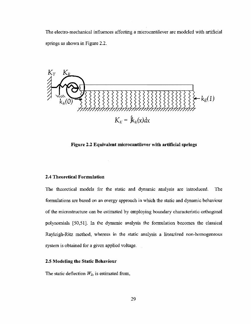
The electro-mechanical influences affecting a microcantilever are modeled with artificial
springs as shown in Figure 2.2.
KE = \kE(x)dx
Figure 2.2 Equivalent microcantilever with artificial springs
2.4 Theoretical Formulation
The theoretical models for the static and dynamic analysis are introduced. The
formulations are based on an energy approach in which the static and dynamic behaviour
of the microstructure can be estimated by employing boundary characteristic orthogonal
polynomials [50,51]. In the dynamic analysis the formulation becomes the classical
Rayleigh-Ritz method, whereas in the static analysis a linearized non-homogeneous
system is obtained for a given applied voltage.
2.5 Modeling the Static Behaviour
The static deflection Ws, is estimated from,
29

Ws(x) = ^Af^)
(2.1)
where the, Af, are the static deflection coefficients of the beam, and <j>i, are the
orthogonal polynomials, x, is a non-dimensional quantity equal to £, IL and varies from 0
to 1, n is the total number of polynomials in the set. The strain energy of the beam is
given by,
Eh'w i
JF(x)(Ws"(x))2dx 2 4 J L ° (2.2)
Where E is the elastic modulus, L is the length of the cantilever, w is the width, h is the
thickness, F i s a geometry conditioning function and Ws"is the second derivative with
respect to x. For the static analysis, the electrostatic potential energy is given by [22],
srsaLwVl f ^ . J , . Ws{x) _ [Ws(xy
(2.3) UP=-^— \F(x)\l + JF(x)\
2d J I d s
\ d dx
where third and higher order terms are ignored. Here, W$ is the static deflection for a
given applied voltage V, so and sr are the permittivity of free space and relative
permittivity of the dielectric medium, respectively, and d is the dielectric gap. In the case
of an electrostatically actuated cantilever, the static equilibrium position is obtained from
the condition,
d
dA [UB+UE] = 0 (2.4)
The above equation results in the following linear system,
30

n 1
7=1
V7 = !...«
(2.5)
where the following definitions apply,
i
Ef = \F(x)fi{x)fj{x)dx o
i
» _ £0£,.w£V2 * _ f0£-rwZ4F2 _ wA3
1 £/J3 > K2 2£/J2 ' " I T
(2.6)
(2.7)
(2.8)
where / is the moment of inertia. One could obtain the static behaviour using Equation
(2.5) for a given voltage. Static behaviour for various applied voltages on SOI MicraGem
cantilever whose specification given below in Table 2.1 where calculated using the model
described above.
Parameter Considered
Length of the cantilevers (L)
Thickness (h)
Maximum width (w(x))
Dielectric gap(do)
Young's modulus E
Density p
Values
810um (measured)
10.5 (am (measured)
90um (measured)
~11 [im (measured)
129.5 GPa (values given by the manufacturer)
2320kgm"3 (values given by the manufacturer)
Table 2.1 Specification of the SOI MicraGem Cantilever
31
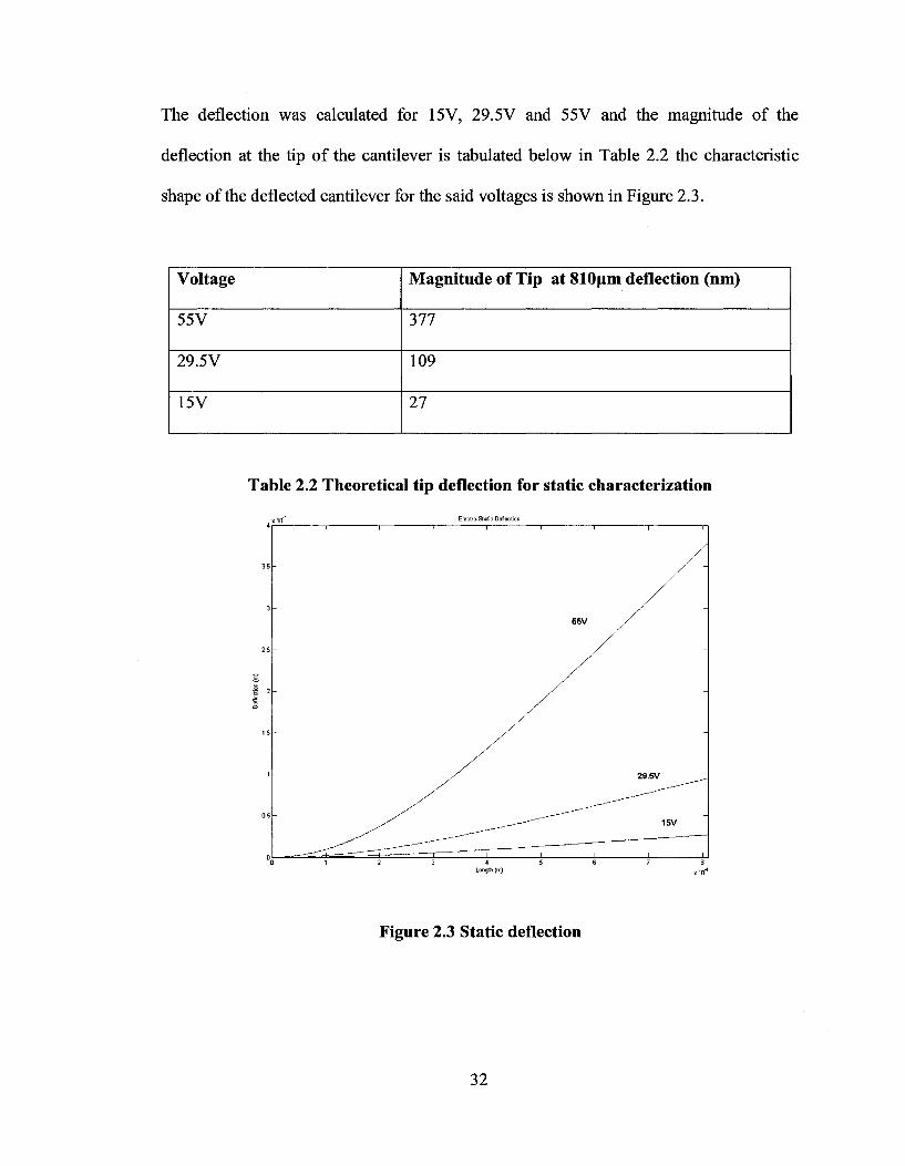
The deflection was calculated for 15V, 29.5V and 55V and the magnitude of the
deflection at the tip of the cantilever is tabulated below in Table 2.2 the characteristic
shape of the deflected cantilever for the said voltages is shown in Figure 2.3.
Voltage
55V
29.5V
15V
Magnitude of Tip at 810um deflection (nm)
377
109
27
Table 2.2 Theoretical tip deflection for static characterization
„ ^o"7 Electro-Slatic Deflection
Figure 2.3 Static deflection
32

2.6 Modeling the Dynamic Behaviour
The estimation of the natural frequencies and mode shapes of the AFM cantilevers are
carried out using the normal mode approach by applying boundary characteristic
orthogonal polynomials in the Rayleigh-Ritz energy method [50]. This approximate
numerical method is a simple way to analyze the flexural response of variety of structures
such as beams and plates [51,52,54] and is employed here for this reason.
The assumed dynamic deflections WD, of the cantilever beam are given by,
FPi>(*)=5X4(*)
(2.9)
where A? are the dynamic deflection coefficients of the beam. The natural frequencies a>k (rad/s), of the system can be obtained by minimizing the Rayleigh quotient defined
as,
„ 2 '-'MAX CO —
TMAX (2.10)
where UMAX, is the maximum strain energy. In this analysis, the total strain energy of the
cantilever system is given by,
UMAX=UB (2.11)
where UB is given by,
UB = Eh'w1
B 241? \P(x)(WD"{x))2dx
(2.12)
The maximum kinetic energy TMAX, is defined by,
TMAX =TB=CQ TMAX (2.13)
and is given by,
33

_ co phwL 1B - z JF(x)(WD(x)fdx
0 (2.14)
where p is the material density. For the dynamic analysis, an artificial electrostatic
stiffness per unit length is obtained from the static equilibrium position of the cantilever
for a given applied voltage, and is given by
kE{x) = s0srw. >£V- F(x)
EI [{d-Ws(x)y
The electrostatic potential energy for the dynamic analysis is then given by,
1 V UED=-\kE{x)(WD(x))2dx
(2.15)
(2.16)
where Ws has been replaced by WD for the dynamic analysis of the flexural deflection of
the cantilever. Minimizing Equation (2.10) with respect to the deflection coefficients^,
results in an eigensystem that uniquely characterizes the dynamic behaviour of the
cantilever. The eigensystem obtained is given by,
yk.22-t/FD-V^00l40=o Z-iL 'J ED "K ^ y X J (2 17)
\fi = l...n
Where the following definitions apply,
2 = coK2phL4
K EI
Solution of Equation 2.17 will provide the natural frequencies and mode shapes for n
number of modes. Dynamic behaviour for 1st and 2nd natural frequency of AFM
cantilever whose specification given below in Table 2.3 was calculated using the model
34

described above. Shown in Table 2.4 are the calculated natural frequencies compared
with that of the manufacturers' specification. Figure 2.4 shows the normalized 1st and 2n
mode shape obtained using the model.
Parameter Considered
Length of the cantilevers (L)
Thickness (h)
Maximum width (w(x))
Young's modulus E
Density p
Values
350um (measured)
1 urn (measured)
3 5 urn (measured)
169.5 GPa (values given by the manufacturer)
2330kgm" (values given by the manufacturer)
Table 2.3 Specification of AFM Cantilever
Mode
1st
2nd
Natural frequency(simulated)
11.2 kHz
70.4 kHz
Natural frequency (by manufacturer)
10.0 kHz ±~3 kHz
n/a
Table 2.4 Theoretical Resonance Frequency
35

-§
Length (1CTDm)
400 60
20 4 0 Wid th (10-6m)
CD T 3 3
"o. £ < T 3 CD hJ
"(O
E o
~Z.
1
0
-1
-2 0
Length (10-°m) 400 4 0 Width (10'6 m)
Figure 2.4 Analytical Representations of the 1st and 2 Mode Shapes
36

2.7 Summary
Design and modeling of MEMS device is done to understand the electrostatic and
mechanical influences for its static and dynamic behavior. The Rayleigh-Ritz energy
method is implemented for the simulation. The results obtained from the theoretical
model presented here were evaluated experimentally using the developed AOMSI and the
comparisons are shown in chapters 5 and 6.
37
Chapter 3
Experimental Setup of Acousto Optic Modulated
Stroboscopic Interferometer
3.1 Introduction
In this chapter the setup of the Acousto Optic Modulated Stroboscopic Interferometer
developed for static and dynamic characterization of microdevices is detailed.
Stroboscopy creates the illusion of slow-motion. In this regard, stroboscopy has been
widely used in photography and also in industrial applications to freeze the motion of
moving objects. The fundamental principle being that when the strobing frequency is
equivalent to the frequency of the device in periodic motion, the motion appears frozen
and is visualized in a still position. This strobing principle can be exploited in the freeze-
frame visualization of high frequency cyclic motion [28] and hence, applied to high
frequency resonating microstructures. Through the combination of a classical
interferometer and a strobed monochromatic light source, measurement of in-plane and
out-of-plane motions of microstructures is possible with resolution in the order of few
nanometers. In the experimental method presented here, an AOM is used as the strobing
module. This setup is the first of its kind to characterize the static, dynamic and surface
profile characteristics of microstructures using on single equipment with a relatively
simple design.
38

3.2 Basic Layout of the Interferometer
The optical setup of the Acousto Optic Modulated Stroboscopic Interferometer is shown
in Figure 3.1. A 5mW, 632.8nm He-Ne laser source is directed into an AOM positioned
at a Bragg angle (0B), of 0.7mrad with respect to the laser so as to maximize the
efficiency of the first order diffraction. The AOM is excited at its center frequency of
85MHz, using a driver. A function generator is employed to modulate the AOM for
strobing the laser at a desired frequency. When the crystal in the AOM is excited it
creates an acoustic grating which splits the single incident laser beam into two optical
outputs, the zero and the first order Bragg diffractions when the AOM is placed in the
Bragg angle with respect to laser. Two y(~ mirrors are used to widen the zeroth and
first order diffractions. The zeroth order Bragg diffraction is terminated and the first order
diffraction is then used for the experiments. The excitation is controlled with the TTL
signal of the function generator which creates the time delay to modulate the first order
diffraction beam which is used for measurements. A spatial filter is used to remove the
spatial error in the optical path in order to obtain a smooth Gaussian beam profile [53,55].
The spatial filter employed here consists of a 10X objective lens, and 40um pinhole and
is used on the first order diffraction.
The interferometer configuration employed in the experimental setup is a Twyman-Green
interferometer which consists of a polarizing beam-splitter cube, two quarter wave plates,
and a reference mirror [29]. The advantage of using a Twyman-Green interferometer is
the capability to control the intensity of the optical beam. In this aspect, the ability to
control the optical intensity is important with regards to the material of the microstructure
39

being tested [45]. The polarizing beam-splitter divides the laser beam into two paths, one
for the reference mirror and one for the microstructure and the quarter wave plates
ensures the directional continuity of the optical path to the CCD camera [56,57]. Lens LI
is used to collimate the laser beam from the spatial filter. The collimated laser beam is
passed through a lens pair of L2 and a microscope objective to define the field of view.
Lens L3 is used for imaging the object onto the focal plane of the CCD camera which is
connected to a data acquisition card. This module helps in transferring all the images
captured in given time frame for further processing. A schematic overview of the layout
is given in Figure. 3.1. A digital image of the experimental setup is shown in Figure. 3.2.
40

[M - Mirror; AOM - Acousto-Optic Modulator; S - Spatial Filter ; LI - 100mm Collimating Lens ; L2 - 150mm Focusing Lens; O - 50mm Microscopic Objective; QW -Quarter Wave Plate; L3 - 300mm Imaging Lens; C - CCD camera; PBS -Polarized Beam
Splitter, PI - polarizer, SI - Stopper]
Figure 3.1 Schematic overview of the principal components in AOMSI
41

Twyman-Green interferometer assembly CCD camera
Figure 3.2 Digital image of the layout of the AOMSI assembly
3.3 Systematic Design and Alignment of the Optical System
The interferometer is built on a coherent optical path. The optical path needs to have
extra attention in order to build a reliable setup of interferometer, therefore extra care
should be given on every level of the setup to make sure that optical system is straight
and aligned. Initially the He-Ne laser is mounted on a holder. The laser is aligned straight
to a given reference. In the setup the mounting hole on the vibration isolation table is
taken as reference to align the optical path and pinhole to align the height. The laser is
42
made to impinge on the AOM mounted on a stage that has 3 degrees of freedom to
control the tilt, height and angle. This enables to properly align the crystal of the AOM
with that of the incoming laser beam. The AOM is then connected to the output of the
SMA (SubMiniature version A) connector of the RF driver using a 50 ohm impendence
matched cable. The AOM is customized for an 0.5mm input beam with an active aperture
of 0.8mm, that enables the laser to be directly passed on to the crystal without focusing.
The AOM is adjusted to the Bragg angle of 0.7 mrad with respect to the laser [65]. When
the laser beam intersects with the acoustic wave at the Bragg angle, there is first order
and zero order beams getting diffracted from the AOM, as described earlier. Due to very
small distances between the 0th and 1st order beams, two mirrors are used to increase the
distance between them. The 0th order beam is then purged and the modulated 1st order
beam is passed onto the spatial filter before being used for measurement.
Due to contaminants in the atmosphere the laser beam has spatial disturbances that can
affect the accuracy of measurement. In order to filter these disturbances and to achieve
uniform intensity, the measurement beam is spatially filtered. A spatial filter assembly
consisting of an objective lens, pinhole, alignment system, and focusing axes can be used
to remove the undesirable noise while transmitting most of the beam's energy. Here a
10X objective and (|)40um pinhole is used to obtain a uniform beam output for our optical
setup. The spatially filtered laser beam is collimated using a lens of 100mm focal length
which increases the beam diameter to 4mm.
43
The collimated laser beam is passed through a lens pair of L2 of 150mm focal length and
a microscopic objective O of 50mm focal length placed 200mm apart. The object is
placed on the focal plane of the objective lens to define the field of view. The reflected
beams from the object pass through objective lens and Lens L3 of 300mm focal length
which images the object onto the CCD sensor. To get a sharp focus CCD sensor of the
camera which is connected to a data acquisition card is positioned 300mm from Lens L3.
The CCD camera used in our system is progressive scan CCD with 648X492 active
pixels with sensor size of 4.9X3.7mm.This optical arrangement gives us the field of view
of 816X616 um over the entire sensor and 1.1667um per pixel.
3.4 Fringe Analysis using Fourier Transformation
In Fourier-transform method, intensity distribution I(x,y) of the interferogram is fitted
with a linear combination of harmonic spatial functions[48].
I(x,y)=a(x,y)+b(x,y)cos[<D(x,y) + 27if0x] (3.1)
where fo is the carrier frequency in the x-direction. Below in Figure 3.3(a) is the
interferogram where the fringe is formed by two X/10 mirror by the interferometer.
44

Methodology for static charactrization of vibrating microstructure
(a) (b)
Figure 3.3 (a) Interferogram (b) Spectrum image of the interferogram
The interferogram is then processed using FFT (Fast Fourier Transform) method to
obtain the spatial frequency. The intensity is resolve into the equation below in the
interferogram on each pixel.
I(x,y)=a(x,y)+c(x,y)+c*(x,y) (3.2)
Where c(x,y)= Y2.b(x,y). exp[i 8 (x,y)] (3.3)
Here the symbol * denotes the complex conjugation and C is the complex Fourier
amplitudes. The spectrum image above shows the both complex conjugation amplitudes
of the interferogram in x- direction.
In the spectrum I(x,y) is a hermitean distribution in the spatial frequency domain. Using
an adapted bandpass filter the unwanted additive disturbances can be eliminated together
with the mode C or C* as show in Figure 3.3(b). Performing an inverse Fourier
transform on the filtered image gives the phase value calculated using Equation 3.4.
8 (X y)= arctan [Im(C( x y)/ Re (C (x y)] (3.4)
45

Figure 3.4(a) below shows the band pass-filter and Figure 3.4(b) shows the result of
inverse Fourier transform which gives a discontinuous phase image. The 2D line profile
of the discontinuous phase image is shown in Figure 3.5. Taking into account the sign of
the numerator and the denominator from Equation 3.4 the principal value of the arctan
function having a continuous period of 2n is reconstructed.
(a) (b)
Figure 3.4 (a) Band - pass filter mask (b) Inverse transform image of the
interferogram
3.1
7.5e-06
-3.1
0 255 511
Figure 3.5 2D profile of the discontinuous image
46

The final step in fringe processing is to obtain a continuous phase from the wrapped mod
27t discontinuity. This process is called unwrapping where depending on the slope; a
value of 2n is either added or subtracted along a line where phase jumps from 0 to 2n in
order to obtain continuity. Figure 3.6 below shows 2D line profile of the continuous
phase obtained from the discontinuous line profile in Figure 3.5.
-2.2 " ~ " ~ ^ - ^
-25 - ^ ^ ^ ~ ^ ^ - - ^ _
-47 — ^ , ! 0 255 511
Figure 3.6 2D profile of the continuous profile
In the Figure 3.6 above, the X axis exhibits the field of view in pixels. The Y axis shows
the displacement of the object in terms of unit less phase value that needs to be quantified
in meters. A sensitivity analysis is done using two A/10 mirrors to quantify this phase
value which is discussed further.
3.5 Sensitivity Analysis
To identify sensitivity, a A/10 mirror is used as an object. Since the reference mirror is in
line with the camera the new object mirror is adjusted to get straight fringes on the
camera. Obtaining straight line fringes in any direction proves that the optical setup is
prefect and the optical path of the interferometer is giving planar wave fringes. With this
we change the angle of the object mirror and capture images with different number of
fringes to calculate the sensitivity of the system. The field of view, as discussed earlier,
for each pixel is calculated to get the distances between the fringes. In planar wave
47
interference, the distances between the fringes depend on the wavelength of the
interfering beams and the half angle between them as shown Figure 3.7. The angle of the
interfering beam can be calculated using the following Equation 3.5.
d = XI2sm{0l2) (3.5)
Figure 3.7 Planar wave interference, 61= 6>2 = 612 (in Eq: 3.5)[95]
Where d is the distance between the fringes and X is the wavelength of the light source
and #is the angle of interference. The fringes were analyzed using Fourier transform
function of the FringeProcessor™ software [104]. The output of the Fourier transform for
out-of-plane displacement is a unit less phase value. In order to correlate this unit less
phase value to a measurement of displacement in width dimensions, sensitivity is
required. To identify the sensitivity the out-of-plane displacement calculated knowing the
field of view and the angle of interference between the two mirrors at different angles, as
shown in Figure 3.8.
48

Reference Mirror
Out of Displacement
Object Mirror
Field of View
Figure 3.8 Angle between reference mirror and object mirror
When there is change in the angle, the fringe formation is altered in the image. For each
and every angle a respective interferogram was captured and analyzed using
FringeProcessor™. The experiments done with different number of fringes and their
corresponding displacements are shown in Table 3.1.
49
# of Fringes
1
2
5
7
9
10
14
16
19
Interference Angle (rad)
0.0335
0.0535
0.08
0.1195
0.1675
0.199
0.2815
0.339
0.3925
Out of plane displacement (M)
3.64E-07
5.81 E-07
8.68E-07
1.26E-06
1.82E-06
2.16E-06
3.06E-06
3.68E-06
4.28E-06
Phase Value
6.27
12.53
18.55
31.38
43.88
50.16
68.98
75.26
94.05
Table 3.1 Tabulation of number of fringes to out of plane displacement
The out-of-plane of displacement was plotted against the unit-less phase value in the
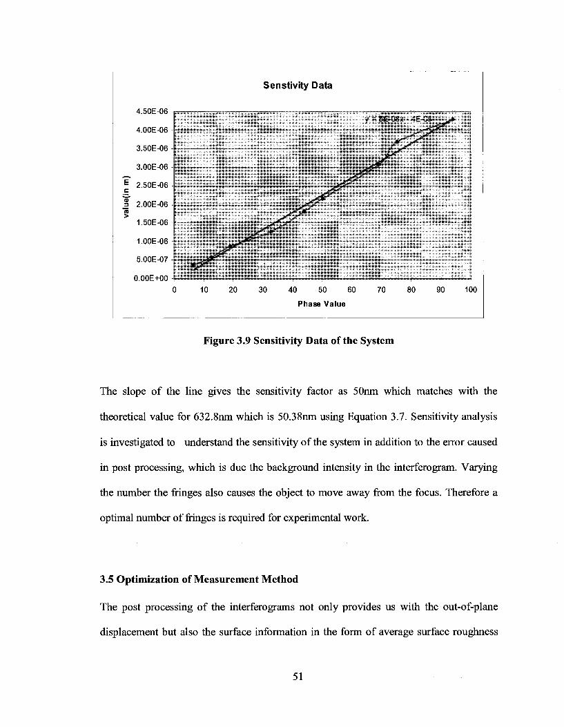
Figure 3.9 to calculate the sensitivity factor.
The sensitivity factor can also be theoretically calculated using Equation 3.6.
2n{Cos<j\ + Cos<p2)
where $ is the phase value, /lis the wavelength, 6\ and 6 2 are the angle of incidence
and angle of reflectance of the laser beam with respect to object normal. For designed
optical system the <f> \ = ^2 = 0 which reduces the Equation 3.6[61] to
h = \®/4n (3.7)
50
4.50E-06 -i
A nflF-Ofi
3.50E-06
•J nnF-OR
E 2.50E-06 -
22 o nnP-fifi -
1.50E-06
1.00E-06
5.00E-07
n nnF+nn -
0 10 20
Senstivity Data
30 40 50 60
Phase Value
y = 5 E - 0 8 x - 4 E - 0 8 ^ ^ »
70 80 90 100
Figure 3.9 Sensitivity Data of the System
The slope of the line gives the sensitivity factor as 50nm which matches with the
theoretical value for 632.8nm which is 50.38nm using Equation 3.7. Sensitivity analysis
is investigated to understand the sensitivity of the system in addition to the error caused
in post processing, which is due the background intensity in the interferogram. Varying
the number the fringes also causes the object to move away from the focus. Therefore a
optimal number of fringes is required for experimental work.
3.5 Optimization of Measurement Method
The post processing of the interferograms not only provides us with the out-of-plane
displacement but also the surface information in the form of average surface roughness
51
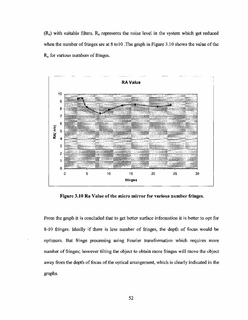
(Ra) with suitable filters. Ra represents the noise level in the system which get reduced
when the number of fringes are at 8 to 10 .The graph in Figure 3.10 shows the value of the
Ra for various numbers of fringes.
Figure 3.10 Ra Value of the micro mirror for various number fringes.
From the graph it is concluded that to get better surface information it is better to opt for
8-10 fringes. Ideally if there is less number of fringes, the depth of focus would be
optimum. But fringe processing using Fourier transformation which requires more
number of fringes; however tilting the object to obtain more fringes will move the object
away from the depth of focus of the optical arrangement, which is clearly indicated in the
graphs.
52
3.4 Summary
An optical setup is done on a vibration isolated table as per the schematic layout done for
AOMSI. Instrumentation required for surface profiling, static and dynamic behaviors are
implemented. The camera is connected for real time vision and for capturing static
images. Sensitivity analysis of the tool was carried out and optimization of measurement
methodology was established. The sensitivity factor of the optimized measurement
methodology was found to be in good agreement with reported results.
53
Chapter 4
Surface Metrology and Static Characterization
4.1 Introduction
In the development of microstructure devices, there is a significant focus in the surface
information of the microstructures. Currently, surface profile is studied using scanning
electron microscope (SEM) or AFM. However there are various constraints on resolution
and the types of materials that can be tested [58, 59]. Considering the limitations of these
instruments, which are also expensive, an interferometric optical method [103] can be a
versatile solution. AOMSI is one such instrument designed to give surface information of
the structure in nanometer resolution and static deflections for different loads. It can be
used on any type of material that has a minimum reflectivity around 30%. Presented in
this chapter are the experimental details of surface metrology conducted on a micro-
mirror and low frequency static characterization on micro-cantilever.
4.1 Surface Metrology
A sample surface metrology is presented using a torsional micro-mirror fabricated using
the MicraGeM SOI fabrication process. The surface area of the mirror is 250 x 250um2.
Given in Figure 4.1 is an SEM image of the torsional micro-mirror.
54

Figure.4.1. Torsional scanning micro-mirror fabricated using MicraGeM SOI
technology.
In the experimental setup, a single CCD camera was employed; hence, it was possible to
capture only a single interferogram at one time. The main focus in fringe processing is to
calculate the phase information of the interferograms and the most widely used methods
in optical metrology for fringe processing are either Fourier transformation [44] or phase
shifting methods [45]. Since this interferometer is generally better suited for dynamic
measurements, it is not possible to employ temporal phase shifting. Hence Fourier
transformation was employed in order to obtain the phase information. Shown in Figure
4.2 is a torsional micro-mirror with a characteristic fringe pattern obtained with the
AOMSI.
55
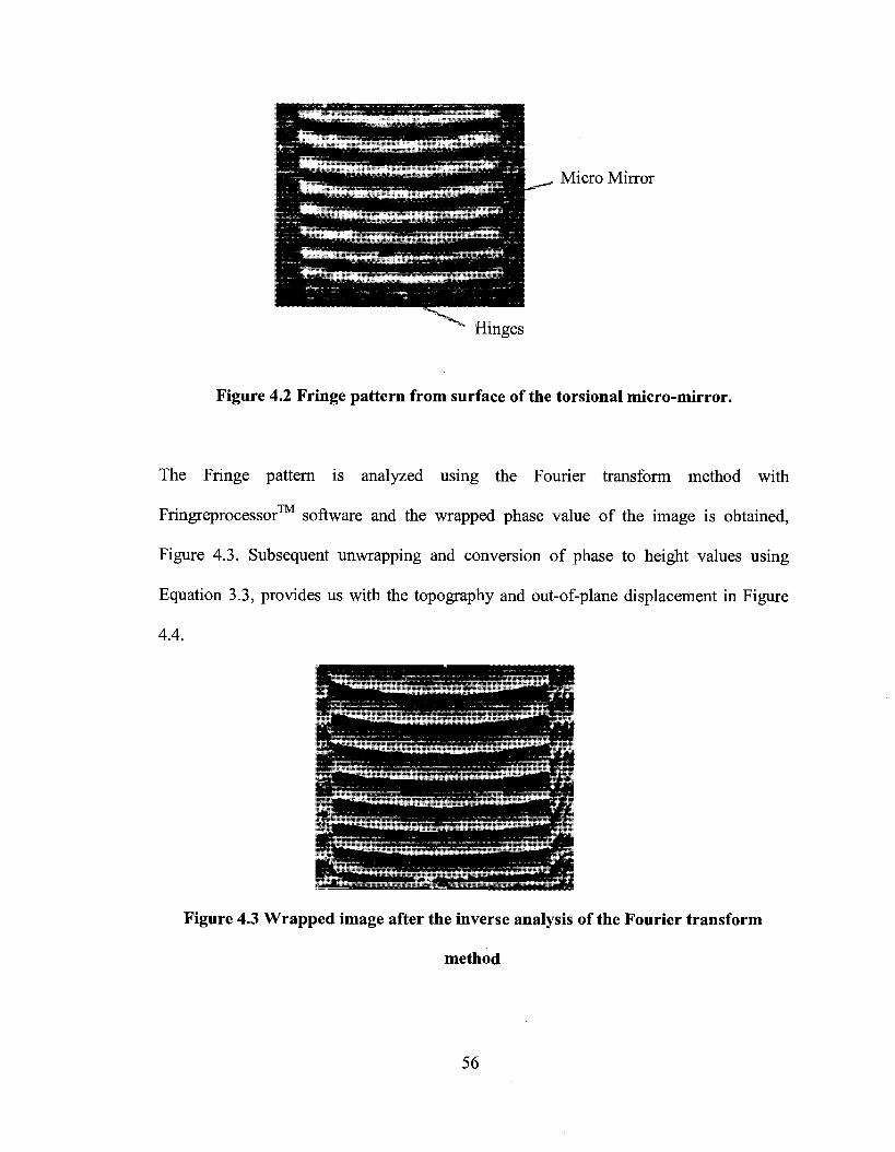
Micro Mirror
Hinges
Figure 4.2 Fringe pattern from surface of the torsional micro-mirror.
The Fringe pattern is analyzed using the Fourier transform method with
Fringreprocessor™ software and the wrapped phase value of the image is obtained,
Figure 4.3. Subsequent unwrapping and conversion of phase to height values using
Equation 3.3, provides us with the topography and out-of-plane displacement in Figure
4.4.
Figure 4.3 Wrapped image after the inverse analysis of the Fourier transform
method
56

Height Information
i no 20C J X -KC 510 fiOO
Pixel value
2D 3D
Figure 4.4 2D and 3D information of the micro-mirror with the tilt information
A least squares fit was carried out on the unwrapped phase image to remove the tilt from
which the surface information is obtained with a resolution of ~10nm. Figures 4.5 and
4.6 represent the surface information obtained for the torsional micro-mirror in 2D and
3D. The micro-mirror tested shows stress formation on the surface [88,11,86].
Dis
plac
emen
t (n
m)
o o
o o
o
o
^ \ ^ _ ^ ^
) 50 100 150 200 250 Number of pixels
300 350 4( 30
Figure 4.5 2D Profile of the surface of the torsional micro-mirror.
57

E c c g "5 a> <D
Q
Number of Pixels
#
0?
*\ Number of Pixels
o
Figure 4.6 Surface characteristics obtained for the SOI torsional micro-mirror. The
curvature and edge deflections are indicators of stress concentrations
4.2 Surface Metrology on a Connecting Pads
The experimental results show the ability of AOMSI to measure the surface profile of a
micro-mirror with nanometer resolution. In order to understand the ability of AOMSI to
characterize devices other than regular mirrors that have depth information, experiments
58

were conducted on connecting pads on a MEMS loose die. Figure 4.7 shows the
interferogram and surface information of MEMS loose die along with the pads taken into
consideration.
Pads
(a) (b)
Figure 4.7 (a) Interferogram (b) Surface information of the surface
4.3 Importance of Static Characterization
MEMS are unique in their integration of electronics and mechanical components within
the design architecture. In this context, intrinsic factors such as mechanical, electrical
and material properties, affecting the performances of MEMS devices, need to be
investigated in order to quantify their combined effect on the static behavior of the
microsystem. In this regard, low frequency static applications, where the repeatability of
the motion after a given time period, include torsional micro-mirrors, micro-switches and
other micro-active-components. These types of devices can be said to operate in a quasi-
59
static state due to the surface motions of these types of micro-devices being much lower
than the natural frequency of the device. Hence, on its own, the analytical model can
only serve to estimate the operational characteristics of the MEMS device, therefore,
experimental testing is needed to augment and complement the theoretical model [87]. In
order to obtain accurate data, specially designed testing methods for microscale devices
are needed [86,74].
In many applications electrostatically actuated MEMS are subjected to dynamic
excitation frequencies well below the natural frequencies of the device. For example,
pressure sensors and scanning mirrors applications require movement of the flexible
structure at frequencies well below the natural frequencies. It can be safely assumed that
at very low frequencies, well below the natural frequencies, the dynamic effects are
negligible. Consider a MEMS device, as shown in Figure 4.8, in which an
electrostatically actuated device is subjected to an external dynamic excitation. In Figure
4.8 the MEMS microcantilever structure is actuated with an applied piezo-electric
mechanical excitation, and an applied DC voltage modeled with artificial electrostatic
spring's kg- In applications where electrostatically actuated MEMS structures are used at
low frequencies, it is important to estimate the behavior of the MEMS structure at these
low excitation frequencies. Even though, the behavior of the structure is close to being
static behavior at very low frequencies, it is important to measure the deflection at lower
excitation frequencies.
60

Piezo-sfiaker
LGM
Figure 4.8 Low frequency excitation using a piezo-stack. Applied electrostatic
potential is modeled with artificial springs kE
This necessitates a method that can measure the static deflection under very low
frequency excitation. Here it proposes an AOMSI based method to measure the static
behavior under low frequency excitation. By tuning the AOM frequencies close to the
excitation frequency, one can measure clearly the deflection. An experiment without
strobing facility would not be able to measure this static behavior.
One of the principal factors to consider is how to perform direct measurements on MEMS
devices in a way that is indicative of the actual micromechanical elements used in the
microsystem. However, due to the micron-scale of MEMS devices, the method used for
the testing must be carefully considered because of the difficulties in directly measuring
forces and other influences at the micro-level. In this regard, the elastic property
61

governing the mechanical qualities of the microsystem, for a given operational
environment, can be deduced through the response of the system to an applied load
[83,6].
A non-contact interferometric optical instrument is a versatile solution for the testing of
the static deflection of MEMS structures. Measurements of surface profiles of MEMS
components are currently achieved by two main techniques, probing methods [5,4] and
optical nondestructive methods [32,85]. Optical methods are advantageous over probe-
based techniques as optical methods are of high speed, non-contact and are capable of
providing full-field results with high spatial resolution [85]. AOMSI is one such
instrument designed to give static surface information and dynamic mode shapes with
nanometer resolution.
In this work, the low frequency static deflection of a MicraGeM technology SOI
cantilever [105] to an applied electrostatic potential is investigated using the AOMSI
approach.
4.4 AOMSI for Low Frequency Static Characterization
The important capability of stroboscopic interferometry compared to other
characterization tools is that it gives a static image of the device through an interferogram
obtained even when the device is in the dynamic state. Interferogram images can be used
to predict the elastic properties of the device more precisely. An overview of the process
is shown in Figure.4.9.
62

(a)
(b)
MEMS Device driven in sinusoidal Signal
Snap Shot of Phase motion
(c)
(a) Surface of MEMS Structure, (b) Driving Frequency and Strobe Frequency, (c) Surface Capture
of the Structure for Various Freeze-Frames.
Figure 4.9 Methodology for static characterization of vibrating
microstructure
In Figure 4.9b, the driving signal for the MEMS device tmems, is triggered at the same time
as the strobing signal tpuise, At is the time delay applied to the strobing signal in order to
capture the surface image with the CCD camera at a position along the dynamic state that
is of interest as shown in Figure 4.9c.
63
With co as the frequency at which the device is driven, it is assumed that,
co = 2nlt mems
In order to obtain static images, the following condition is required
pulse mems
therefore,
*pulse =2X/C0
4.5 Measurement of Static Deflections
Shown in Figure 4.11 is a scanning electron microscope (SEM) image of a MicraGeM
SOI technology cantilever array. In this figure, the length of the cantilevers is 810um,
the thickness was measured as 10.5um, and the maximum width is 90um as shown in
Figure 4.10. The measured dielectric gap was ~1 l|_im. One cantilever was tested device
under test (DUT) at 15V, 29.5V and 55V, respectively. The DUT with fringes at 15V,
29.5V and 55V that were used for computing the deflections are shown in Figure 4.12.
In the theoretical analysis, Young's modulus E was taken as 129.5 GPa, and the density
as 2320kgm" (values given by the manufacturer).
(4.1)
(4.2)
(4.3)
64

Free End
Figure 4.10 Microscopic image of the micragem SOI technology cantilever used for
static deflection experiment.
Figure 4.11 An SEM image of an SOI MicraGem technology cantilever array
As described earlier, a 30Hz progressive scan CCD camera with 648 x 492 pixels is used
to capture the interferogram. The setup allows one to view the microstructure and to
65

evaluate the behavior in real time. Shown in Figure 4.12 are the interference fringes as
seen on SOI MicraGeM cantilever actuated at various static DC voltages.
Figure 4.12 Fringe patterns obtained for the DUT at various voltages, (a) 15V. (b)
29.5V. (c) 55V.
For the characterization of static deflection, the fringe pattern was obtained after strobing
at the same frequency as the excitation (the device was excited at 5% of its natural
frequency). Processing the interferogram as described in described earlier using Fourier
transformation and subsequent filtering, deflection of DUT at various static voltages was
obtained. Shown in Figure.4.13 is the deflections of DUT for three different static
voltages obtained experimentally compared with the theoretical deflection obtained
66
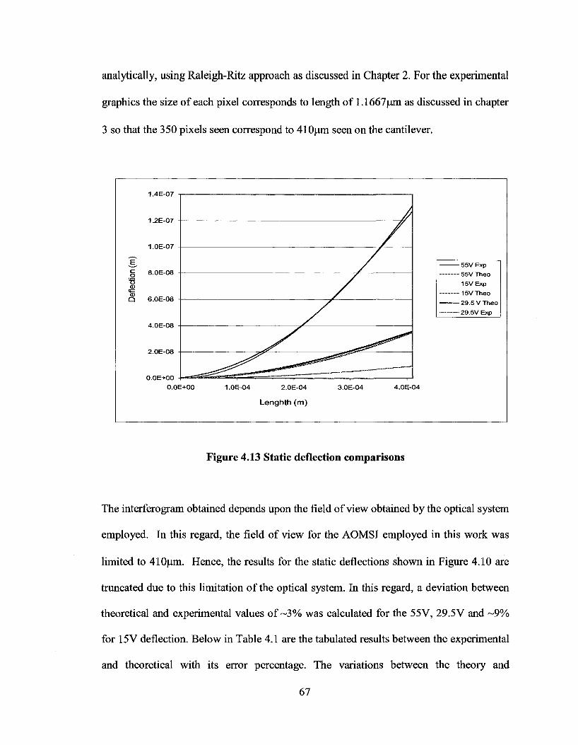
analytically, using Raleigh-Ritz approach as discussed in Chapter 2. For the experimental
graphics the size of each pixel corresponds to length of 1.1667pm as discussed in chapter
3 so that the 350 pixels seen correspond to 410um seen on the cantilever.
o CD
Q
1.4E-07
1.2E-07
1.0E-O7
8.0E-08
6.0E-08
4.0E-08
2.0E-08
O.OE+00 O.OE+OO 1 .OE-04 2.0E-04
Lenghth (m)
3.0E-04 4.0E-04
- 55V Exp - 55V Theo
15V Exp -15V Theo -29.5 V Theo - 29.5V Exp
Figure 4.13 Static deflection comparisons
The interferogram obtained depends upon the field of view obtained by the optical system
employed. In this regard, the field of view for the AOMSI employed in this work was
limited to 410pm. Hence, the results for the static deflections shown in Figure 4.10 are
truncated due to this limitation of the optical system. In this regard, a deviation between
theoretical and experimental values o f - 3 % was calculated for the 55V, 29.5V and ~9%
for 15V deflection. Below in Table 4.1 are the tabulated results between the experimental
and theoretical with its error percentage. The variations between the theory and
67

experimental results are due, in part, to optical effects related to the surface effects of the
reference mirrors. Commercial interferometers employ traceable reference mirrors for
higher accuracy. Since in this setup a normal 7J10 mirror is used as a reference the
resolution of the measurement system is ~10nm. The results tabulated below show clearly
the reliability of measurement above lOnm. However, the results in themselves
demonstrate very good agreement with the analytical model, thereby demonstrating the
sensitivity of the detection methodology and also the suitability of employing this
approach for microstructure static analysis.
Voltage
15V
29.5V
55V
Magnitude of Tip deflection (nm)
at 410 fim (Theoretical)
9.12
36
126
Magnitude of Tip deflection
(nm) (Experimental)
8.01
34.8
130
Error
-9%
-3%
-3%
Table 4.1 Tip deflection of the DUT for static characterization
68
4.6 Summary
Experiments were done for surface profiling on a micro-mirror. 2D and 3D profiles of
the micro-mirror and the connecting pads were measured. The out-of-plane curvature
profiled was attributed to the internal stress formation on free-standing microstructures.
Static characterization methodology and experimental results were presented on micro-
cantilever vibrating at 5% of their natural frequency. The results of low frequency static
characterization found to be in good agreement with the theoretical predictions.
69

Chapter 5
Dynamic Characterization
5.1 Introduction
Presented in this chapter are the experimental studies of dynamic behavior on AFM
cantilever. The length, width and thickness of the test structure are 350um, 35um and
1 um, respectively. The density of the single-crystal-silicon used is 2330kgm"3 with an
elastic modulus of 169.5 GPa. The methodology and process to conduct dynamic test on
AOMSI are detailed out. The mode shapes obtained from the experiments are compared
with the simulated mode shapes. The^SEM image of the device under test (DUT) is show
in Figure 5.1
Figure 5.1 SEM image of the AFM Cantilever
70
5.2 Dynamic Characterization
Dynamic characterization gives the performance evaluation of a device. While
performing dynamic characterization on a MEMS device the device performs is
investigated in its working state. Due to the extremely small size nature of MEMS device
very few tools have been developed (eg: LDV) for understanding the dynamic nature of
the MEMS device. AOMSI finds a huge possibility for this type of characterization and
has capability to extend it testing capacity to device with higher natural frequency.
Compared to other testing method, AOMSI enables high speed visualization of dynamic
objects because of its strobing nature. The interferogram of dynamic objects provide
higher resolution and higher sensitivity displacement measurements. It can also give
details of all the response of the device like various vibration mode shapes.
Figure 5.2 gives details of dynamic characterization on a MEMS device In order to
capture the displacement of the device in slow motion there is very small difference 8t
between the strobing frequency and the driving frequency of the MEMS device. In a
periodic motion this difference will help is capturing the motion part by part in a given
time frame, so that a standard CCD camera can be used for capturing high-speed motion.
71

MEMS Device driven in sinusoidal Signal
Snap Shot of Phase motion
Figure 5.2 Methodology To Conduct Dynamic Characterization
While keeping the same terms as that of static characterization and introducing 8t as the
difference in the frequency it describe the process in mathematical terms for out-of-plane
displacement as follows.
From Equation
tpulse ~ *MEMS = ™ W • 1)
tp&e-nlnlco^dt
tp«ise=n2x/o> + nSt
(5.2)
(5.3)
Forn=0, 1,2
72

t2=4x/a>+2St (5.4)
t3 =6nl co + 38t
From the above equation 8t plays a vital role in dynamic characterization. The smaller the
5t more the number of frames per cycle. In this work we use frame grabber card so
different frames where captured manually. Using a data acquisition card will enable the
automation of the image capture to various level of detail. With the developed system
dynamic behavior of microdevices actuated by different mechanisms can be studied
under various environmental conditions. For example a microcantilever can be actuated
either using electro static force or piezo stack to its natural frequency. The system can
also be used in vacuum or non-vacuum condition to see the Q-factor of the device.
To prove the concept of dynamic characterization using AOMSI experiments have been
conducted on AFM cantilever for detecting its natural frequency and mode shape in its
first and second mode of vibrations. The experiments were conducted in non-vacuum
conditions. The mode of excitation was using a piezo stage connected to a function
generator. The stage was excited using a sinusoidal function.
5.3 Identification of Natural Frequency
The AFM tip is carefully mounted on a piezo stage which is mounted on a six axis stage
of the AOMSI. Initially the laser is strobed at higher frequency (1 MHz). The AFM tip is
focused with desired number of fringes on it. When the AFM is mounted perfectly the
73

piezo stage is connected to the function generator for detecting the various natural
frequencies of the device. Along with the mode shapes, the 1st and 2n natural frequencies
of the AFM cantilever were also determined. This was achieved, initially, by monitoring
the surface motion of the cantilever for a given swept frequency range. The upper bracket
of the frequency range was then reduced incrementally in such a manner to obtain a low
amplitude surface motion of the device, similarly, the lower frequency bracket was
gradually increased to obtain an equal surface displacement as for the upper bracket.
Hence, by using this approach, the shoulders of the resonance frequency response curve
were obtained, from which the average of the two values resulted in the center frequency,
or resonance frequency of the AFM cantilever. This method was applied for several
different lower and upper shoulder values, and an average of the center frequencies
obtained was then taken. The experimentally determined 1st and 2nd natural frequencies
were 10.7 kHz and 74.6 kHz, respectively. These values are in good agreement with the
theoretical values of, 11.2 kHz and 70.4 kHz, for the 1st and 2n natural frequencies,
respectively. The manufacturer supplies a nominal value of 10.0 kHz ± ~3 kHz.
Mode
1st
2nd
Natural
Frequency(simulated)
11.2 kHz
70.4 kHz
Natural frequency
(from manufacturer)
10.0 kHz ±~3 kHz
n/a
Natural
frequency(Experimental)
10.7 kHz
74.6 kHz
Table 5.1 Comparison of natural frequency
74
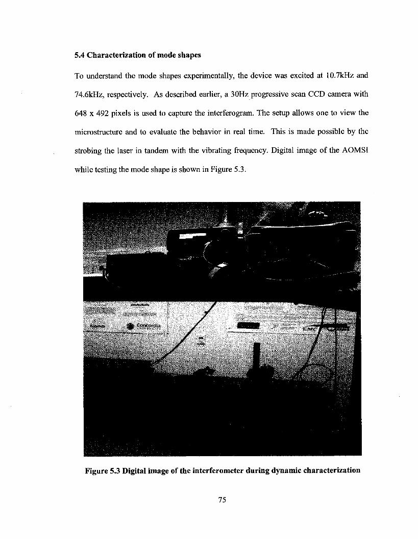
5.4 Characterization of mode shapes
To understand the mode shapes experimentally, the device was excited at 10.7kHz and
74.6kHz, respectively. As described earlier, a 30Hz progressive scan CCD camera with
648 x 492 pixels is used to capture the interferogram. The setup allows one to view the
microstructure and to evaluate the behavior in real time. This is made possible by the
strobing the laser in tandem with the vibrating frequency. Digital image of the AOMSI
while testing the mode shape is shown in Figure 5.3.
Figure 5.3 Digital image of the interferometer during dynamic characterization
75

The oscilloscope is used to control the 8t to enable manual triggering of the frame
grabber card so that the interferograms can be captured at the desired position. Shown in
Figure 5.4 are the interference fringes as seen on tipless AFM cantilevers. In this figure,
for the middle, and bottom frames the device was driven at the 1st and 2nd resonance
frequency, respectively.
For the dynamic flexural mode shapes, the AOMSI method was applied to the AFM
cantilever (DUT). In this manner the 1st and 2" mode shapes were obtained. Higher
order modes are also possible; however the limitation of the piezo-excitation source must
be considered [2]. Processing the interferogram as described in chapter 4 using Fourier
transformation and subsequent filtering, mode shapes of DUT was obtained. Shown in
Figure 5.4 is the mode shape of 1st natural frequency at 10.7 KHz obtained
experimentally. The three dimensional mode shape obtained experimentally is compared
with the mode shape obtained analytically, shown in Figure 5.5 using Raleigh-Ritz
approach as discussed in chapter 2. Similarly experiments where done on 2nd natural
frequency of 74.6 KHz, for which experimental and analytical mode shapes are shown in
Figure 5.6. For the experimental graphics the size of each pixel corresponds to length of
1.1667um as discussed in chapter 3 so that the 300 pixels seen correspond to 350um.
76

(a)
(b)
(c)
• • 4 «• . .
DUT
ft.0- •£ * * $ ^
** S '^V'y^3^^*??»j |B^*18^S Highly deflected portion
Node
Highly deflected portion
Figure 5.4 The observed fringe pattern obtained seen on AFM cantilevers, a)
Device-Under-Test (DUT). b) 1st resonance mode, c) 2nd resonance mode.
77
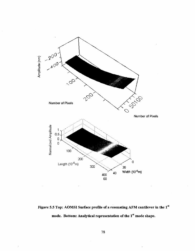
E c
<D
"5. E <
Number of Pixels
<n T3 13
• » - *
"5. E < 13 (U N
Length (10-°m)
400 60
Number of Pixels
4 0 Width (10-bm)
Figure 5.5 Top: AOMSI Surface profile of a resonating AFM cantilever in the 1st
mode. Bottom: Analytical representation of the 1st mode shape.
78

e c T3
"Q. E <
Number of Pixels
Number of Pixels
a. E < T3 CD N
Length (ICTm) 400 4 0 Width (1Q-6 m)
Figure 5.6 Top: AOMSI surface profile of a resonating AFM cantilever in the 2 nd
nd mode. Bottom: Analytical representation of the 2 mode shape.
79
5.5 Summary
Experiments were done to characterize the dynamic behavior of AFM cantilever.
Experimental methodology for identifying the natural frequency was presented. The
experimentally determined 1st and 2nd natural frequencies were found to be within the
manufacturer's specification and the theoretical predictions. Further experiments were
done to profile the 1st and 2n mode shapes. The normalized mode shapes obtained
experimentally were in good agreement with those obtained from the theoretical model.
80
Chapter 6
Conclusion
6.1 Conclusion
Design and modeling of a simple MEMS device was simulated to understand the
mechanical influence on its static and dynamic behavior using Raleigh-Ritz method. A
simple yet viable Acousto Optic Modulated Stroboscopic Interferometer (AOMSI) is
developed using a frequency stabilized CW laser together with an Acousto Optic
Modulator for comprehensive mechanical characterization. The designed interferometer
was setup on a vibration isolation table to conduct experiments on microstructures. The
real-time vision system was employed on the interferometer to visualize high speed
motion and to capture static images of those motions. An optimized methodology for
measurement was established and sensitivity analysis was conducted.
Experiments for surface profiling were done on a micro-mirror. The 2D and 3D profile
was measured. The out-of-plane curvature found on the micro-mirror was attributed to
internal stress formation in the microstructure. Additional surface characterization on
MEMS loose die with pads on them was done. The ability of the stroboscopic
interferometry to perform measurements accurately on dynamic microstructures was
presented in two scenarios, where the microstructures was made to vibrate at 5% of its
natural frequency and static deflection to various DC electrostatic voltages were studies
in the low frequency static characterization. The results showed good agreement with the
theoretical model. The error in comparison between the experimental and theoretical
81
static influences was ~ 3 % for deflections higher than lOnm. The errors for tip deflections
below lOnm were found to be having a higher error percentage which clearly
demonstrates the ability of the experimental tool to measure reliably with a resolution of
about lOnm.
To further test the ability of dynamic characterization, an AFM cantilever was excited at
its natural frequency and the assessment of dynamic behavior was demonstrated.
Identifying the natural frequency and modal profile for 1st and 2nd resonance frequencies
was carried out. The comparison with the theoretical model showed good agreement and
reliability of the AOMSI for investigation of dynamic parameters. The experimental
methodology mentioned above explored the feasibility of conducting Fourier transform
for fringe processing on a stroboscopic interferometer. The approach is first of its kind
developed to investigate the surface, static and dynamic behavior of microstructures
using a single tool. Thus the concept of single multi-functional tool to conduct
comprehensive mechanical characterization on microstructures was developed.
6.2 Future Work
From the perspective of high precision metrology, objective for improvisation to build
and design better characterization tool, opened new approaches on various stands and a
few of them are discussed further in recommendation for future work.
Acousto Optic Modulated Stroboscopic Interferometer was built on a vibration isolation
table. The setup was developed using open optics with an array of lens and mirrors. The
82

main constraint was alignment of the optical path through these arrays of optics. It gave
us the advantage on various fronts to modify and change the design during the setup.
Since the concept is in the stage of maturity, implementation of fiber-optic in AOMSI is a
good advancement. It makes its more compact, portable and improves spatial resolution
of the tool, in addition to removing noises due to reflections from the various free space
optics. To improve the resolution of the AOMSI one of the recommendation is
implementation of spatial phase-shifting method. It complicates the experimental setup to
a certain extend but can be compromised on for higher out-of-plane resolution to an order
of ~ 0.1 to 1 nm. During the post processing of interferogram various image filtering
technique were implemented to compensate on the surface profile effect of the reference
mirror (A/10). A solution to enhance the resolution and also improve the tool would be
implementation of a reference mirror that has traceability [106] to National Standards, as
is done in commercial interferometers. AOMSI has modulation capability of 4 MHz as
designed, but this can be improved up to 85 MHz by implementing a focus system in
front of the AOM to reduce the beam diameter of the laser.
83

References
[1] Rebello, KJ.,(2004), "Applications of MEMS in Surgery" Proc IEEE, 92(1), pp.43-
55.
[2] www.piezomechanik.com,(2006), "Piezomechnik technical data
sheet"(chk:March2008)
[3] Smith, C.S.,(1954), "Piezoresistance Effect in Germanium and Silicon" Physical
Review, 94(1), pp.42-49.
[4] Oliver, W. and Pharr, G.,(1992), "An Improved Technique for Determining Hardness
and Elastic Modulus Using Load and Displacement Sensing Indentation Experiments"
J.Mater.Res., 7(6), pp. 1564-1583.
[5] Knapp, J.,(1999), "Finite-element modeling of nanoindentation" J.Appl.Phys., 85(3),
pp.1460.
[6] Rinaldi, G., Packirisamy, M. and Stiharu, I.,(2006), "Boundary characterization of
microstructures through thermo-mechanical testing" J Micromech Microengineering,
16(3), pp.549-556.
[7] French, P. and Evans, A.,(1985), "Polycrystalline Silicon Strain Sensors" ECS.
[8] Hogarth, C.,(1964), "Semiconductor transducers" British Journal of Applied Physics,
15(2),pp.l21-130.
[9] Petersen, K.,(1982), "Silicon as a mechanical material" Proc IEEE, 70(5), pp.420-
457.
84

[10] Hirano, T., Furuhata, T., Gabriel, K. and Fujita, H.,(1992), "Design, fabrication, and
operation of submicron gap comb-drivemicroactuators" Microelectromechanical Systems,
Journal of, 1(1), pp.52-59.
[11] Yamaguchi, M. And Kawaguchi, S.,(2006), "Study of experimental mechanical
stress characterization of MEMS by using of confocal laser scanning microscope with a
Raman spectroscopy interface", pp.21-35.
[12] Angell, J., Barth, P. and Terry, S.,(1983), "Silicon micromechanical devices"
Sci.Am., 248pp.44-55.
[13] Lee, J.D., Yoon, J.B., Kim, J.K., Chung, H.J., Lee, C.S., Lee, H.D., Lee, H.J., Kim,
C.K. and Han, C.H.,(1999), "A thermal inkjet printhead with a monolithically fabricated
nozzleplate and self-aligned ink feed hole" Microelectromechanical Systems, Journal of,
8(3), pp.229-236.
[14] Petersen, K.,(1979), "Fabrication of an integrated, planar silicon ink-jet structure"
Electron Devices, IEEE Transactions on, 26(12), pp. 1918-1920.
[15] Fan, L.S., Tai, Y.C. and Muller, R.,(1989), "IC-processed electrostatic
micromotors." Sensors Actuators., 20(1), pp.41-47.
[16] Feynman, R.,(2002), "There's Plenty Of Room At The Bottom" Feynman and
Computation: Exploring the Limits of Computers,
[17] Kim, S., Barbastathis, G. and Tuller, H.,(2004), "MEMS for Optical Functionality"
Journal of Electroceramies, 12(1), pp. 133-144.
[18] Fujita, H.,(1997), "A decade of MEMS and its future" Micro Electro Mechanical
Systems, 1997MEMS'97, Proceedings, IEEE., Tenth Annual International Workshop on,
pp.1-7.
85

[19] Yazdi, N., Salian, A. and Najafi, K.,(1999), "A high sensitivity capacitive
microaccelerometer with afolded-electrode structure" Micro Electro Mechanical Systems,
1999.MEMS'99. Twelfth IEEE International Conference on, pp.600-605.
[20] Yazdi, N. and Najafi, K.,(2000), "An all-silicon single-wafer micro-g accelerometer
with a combined surface and bulk micromachining process" J Microelectromech Syst,
9(4), pp.544-550.
[21] Loh, N., Schmidt, M. and Manalis, S.,(2002), "Sub-10 cm 3 interferometric
accelerometer with nano-gresolution" Microelectromechanical Systems, Journal of,
11(3), pp. 182-187.
[22] Rinaldi, G., Packirisamy, M. and Stiharu, I.,(2004), "Electrostatic boundary
conditioning of MEMS devices" Proceedings of the 8 thlnternational Cairo University
MDP, Conference on Current Advances in Mechanical Design and Production VIII,
pp.269-276.
[23] Bosseboeuf, A. and Petitgrand, S.,(2003), "Characterization of the static and
dynamic behaviour of M(0)EMS by optical techniques: status and trends"
J.Micromech.Microeng, 13(4), pp.s23-s33.
[24] Danilatos, G.,(1988), "Foundations of environmental scanning electron microscopy"
Advances in electronics and electron physics, 71pp. 109-250.
[25] Gu, M.,(1996), "Principles of Three Dimensional Imaging in Confocal Microscopes"
ISBN 9810225504.
[26] Ehrmann, K., Ho, A. and Schindhelm, K.,(1998), "A 3 D optical profilometer using
a compact disc reading head" Measurement Science and Technology, 9(8), pp. 1259-1265.
86

[27] Quan, C , Wang, S. and Tay, C.,(2006), "Nanoscale surface deformation inspection
using FFT and phase-shifting combined interferometry" Precis Eng, 30(1), pp.23-31.
[28] Krehl, P., Engemann, S., Rembe, C. and Hofer, E.,(1999), "High-speed
visualization, a powerful diagnostic tool for microactuators-retrospect and prospect"
Microsystem Technologies, 5(3), pp.113-132.
[29] Hart, M., Conant, R., Lau, K. and Muller, R.,(2000), "Stroboscopic interferometer
system for dynamic MEMS characterization" Microelectromechanical Systems, Journal
o/9(4),pp.409-418.
[30] Rembe, C , Kant, R. and Muller, R.S.,(2001), "Optical measurement methods to
study dynamic behavior in MEMS" Proc.SPIE, 4400pp. 127-137.
[31] Rembe, C. and Muller, R.,(2002), "Measurement system for full three-dimensional
motion characterization of MEMS" Microelectromechanical Systems, Journal of, 11(5),
pp.479-488.
[32] Osten, W. and Ferraro, P.,(2006), "O Digital Holography and Its Application in
MEMS/MOEMS Inspection" Optical Inspection of Microsystems,
[33] Colomb, T., Marquet, P., Charriere, F., Kuhn, J., Jourdain, P., Depeursinge, C ,
Rappaz, B., Magistretti, P., Prilly, S. and Lausanne, S./'Electronic Imaging & Signal
Processing Enhancing the performance of digital holographic microscopy"
[34] Ngoi, B.K.A., Venkatakrishnan, K. and Tan, B.,(2000), "Laser scanning heterodyne-
interferometer for micro-components" Opt.Commun., 173(1-6), pp.291-301.
[35] Ngoi, B.K.A., Venkatakrishnan, K., Tan, B., Noel, N., Shen, Z. and Chin, C.,(2000),
"Two-axis-scanning laser Doppler vibrometer for microstructure" Opt.Commun., 182(1-
3),pp.l75-185.
87
[36] Ono, N., Kitamura, K., Nakajima, K. and Shimanuki, Y.,(2000), "Measurement of
Young's Modulus of Silicon Single Crystal at High Temperature and Its Dependency on
Boron Concentration Using the Flexural Vibration Method" Jpn.J.Appl.Phys, 39pp.368-
371.
[37] Rinaldi, G., Packirisamy, M. and Stiharu, I.,(2007), "Dynamic testing of
micromechanical structures under thermo-electro-mechanical influences" Measurement,
40(6), pp.563-574.
[38] Stanbridge, A.B., Martarelli, M. and Ewins, D.J.,(2004), "Measuring area vibration
mode shapes with a continuous-scan LDV" Measurement, 35(2), pp. 181-189.
[39] Nakadate, S., Saito, H. and Nakajima, T.,(1986), "Vibration Measurement Using
Phase-shifting Stroboscopic Holographic Interferometry" Journal of Modern Optics,
33(10), pp. 1295-1309.
[40] Rembe, C , Tibken, B. and Hofer, E.,(2001), "Analysis of the dynamics in
microactuators using high-speed cinephotomicrography" Microelectromechanical
Systems, Journal of, 10(1), pp.137-145.
[41] Yang, L. and Colbourne, P.,(2003), "Digital laser microinterferometer and its
applications" Optical Engineering, 42pp.l417.
[42] Kujawinska, M.,"Optical metrology: from micromeasurements to multimedia"
[43] Bracewell, R. and Kahn, P.B.,(1966), "The Fourier Transform and Its Applications"
American Journal of Physics, 34pp.712.
[44] Brigham, E.O.,(1988), "The fast Fourier transform and its applications"
88

[45] Hariharan, P., Oreb, B. and Eiju, T.,(1987), "Digital phase-shifting interferometry: a
simple error-compensating phase calculation algorithm" Appl.Opt., 26(13), pp.2504-
2506.
[46] Schmit, J. and Creath, K.,(1995), "Extended averaging technique for derivation of
error-compensating algorithms in phase-shifting interferometry" Appl.Opt., 34(19),
pp.3610-3619.
[47] Brophy, C.P.,(1990), "Effect of intensity error correlation on the computed phase of
phase-shifting interferometry." Journal of the Optical Society of America A: Optics and
Image Science, and Vision, 7(4), pp.537-541.
[48] Takeda, M., Ina, H. and Kobayashi, S.,(1982), "Fourier-transform method of fringe-
pattern analysis for computer-based topography and interferometry" J.Opt.Soc.Am.,
72(l),pp.l56-160.
[49] Kreis, T.,(1986), "Digital holographic interference-phase measurement using the
Fourier- transform method" Optical Society of America, Journal, A: Optics and Image
Science, 3pp.847-855.
[50] Bhat, R.,(1985), "Natural frequencies of rectangular plates using characteristic
orthogonal polynomials in Rayleigh-Ritz method" J.Sound Vibrat., 102pp.493-499.
[51] Lam, K., Hung, K. and Chow, S.,(1989), "Vibration analysis of plates with cutouts
by the modified Rayleigh-Ritz method" Appl.Acoust., 28pp.49-60.
[52] Liew, K., Kitipornchai, S., Leung, A. and Lim, C.,(2003), "Analysis of the free
vibration of rectangular plates with central cut-outs using the discrete Ritz method"
IntJ.Mech.Sci., 45(5), pp.941-959.
89

[53] Backus, S., Durfee III, C.G., Murnane, M.M. and Kapteyn, H.C.,(1998), "High
power ultrafast lasers" Rev.Sci.Instrum., 69pp. 1207.
[54] Mundkur, G., Bhat, R. and Neriya, S.,(1994), "Vibration Of Plates With Cut-Outs
Using Boundary Characteristic Orthogonal Polynomial Functions In The Rayleigh-ritz
Method" J.Sound Vibrat, 176(1), pp.136-144.
[55] Hoffhagle, J. A. and Jefferson, C.M.,(2000), "Design and performance of a refractive
optical system that converts a Gaussian to a flattop beam" Appl.Opt., 39(30), pp.5488-
5499.
[56] Hasman, E., Bomzon, Z., Niv, A., Biener, G. and Kleiner, V.,(2002), "Polarization
beam-splitters and optical switches based on space-variant computer-generated
subwavelength quasi-periodic structures" Opt.Commun., 209(1-3), pp.45-54.
[57] Gizzi, L.A., Giulietti, D., Giulietti, A., Audebert, P., Bastiani, S., Geindre, J.P. and
Mysyrowicz, A.,(1996), "Simultaneous measurements of hard x-rays and second
harmonic emission in fs laser-target interactions" Phys.Rev.Lett., 76(13), pp.2278-2281.
[58] Breton, P.,(1999), "From Microns to Nanometers: Early Landmarks in the science of
Scanning Electron Microscope imaging" Scanning Microsc, 13(1), pp. 1-6.
[59] Zhong, W., Overney, G. and Tomanek, D.,(1991), "Limits of resolution in atomic
force microscopy images of graphite" Europhys.Lett., 15pp.49.
[60] Binnig, G., Quate, C. and Gerber, C.,(1986), "Atomic Force Microscope"
Phys.Rev.Lett., 56(9), pp.930-933.
[61] Cloud, G.L.,(1995), "Optical Methods of Engineering Analysis" ISBN 0521636426.
90

[62] Petitgrand, S., Yahiaoui, R., Danaie, K., Bosseboeuf, A. and Gilles, J.,(2001), "3D
measurement of micromechanical devices vibration mode shapes with a stroboscopic
interferometric microscope" Optics and Lasers in Engineering, 36(2), pp.77-101.
[63] Kwon, O., Shough, D. And Williams, R.,(1987), "Stroboscopic phase-shifting
interferometry" Opt.Lett., 12(ll),pp.855-857.
[64] Sreenivasan, M.M.P., Sivakumar, N. and Packirisamy, M.,(2006), "Theoretical
modeling of acousto-optic modulated stroboscopic interferometer" Proceedings ofSPIE,
6343pp.634322.
[65] Goutzoulis, A.P.,(1994), "Design and Fabrication of Acousto-Optic Devices" ISBN
082478930X.
[66] Kodama, Y., Romagnoli, M. and Wabnitz, S.,(1994), "Stabilisation of optical
solitons by an acousto-optic modulator andfilter" Electron.Lett, 30(3), pp.261-262.
[68] Eldada, L.,(2001), "Advances in telecom and datacom optical components" Optical
Engineering, 40pp. 1165.
[69] Chang, I.,(1976), "I. Acoustooptic Devices and Applications" Sonics and
Ultrasonics, IEEE Transactions on, 23(1), pp.2-21.
[70] Matsumoto, H. and Hirai, A.,(1999), "A white-light interferometer using a lamp
source and heterodyne detection with acousto-optic modulators" Opt.Commun., 170(4-6),
pp.217-220.
[71] Lawrence, E.M., Speller, K. and Yu, D.,(2002), "Laser Doppler vibrometry for
optical MEMS" Proceedings of the 5th International Conference on Vibration
Measurements by Laser Techniques.Ancona, Italy, pp. 18-21.
91
[72] Speller, K.E., Goldberg, H., Gannon, J. and Lawrence, E.,"Unique MEMS
Characterization Solutions Enabled by Laser Doppler Vibrometer Measurements"
Applied MEMS Inc, 12200pp.77477-72409.
[73] Xing, F., Yun-qiang, L. and Xiao-dong, H.,(2004), "Micro laser Doppler vibrometer
technology for MEMS dynamic measurement" Journal of Optoelectronics- Laser, 15(11),
pp.1357-1360.
[74] Pister, K.SJ.,"Introduction to MEMS Design and Fabrication" EECS, 245pp.9-45.
[75] Judy, J.W.,(2001), "Microelectromechanical systems(MEMS)- Fabrication, design
and applications" Smart Mater Struct, 10(6), pp.1115-1134.
[76] Bao, M. and Wang, W.,(1996), "Future of microelectromechanical systems
(MEMS)" Sensors & Actuators: A.Physical, 56(1-2), pp.135-141.
[77] Madou, M.J.,(1997), "Fundamentals ofmicrofabrication" ISBN 0849394511
[78] Madou, M.J.,(2002), "Fundamentals of Microfabrication: The Science of
Miniaturization" ISBN 0849308267
[79] Noell, W., Clerc, P.A., Dellmann, L., Guldimann, B., Herzig, H.P., Manzardo, O.,
Marxer, C , Weible, K., Dandliker, R. and de Rooij, N.,(2002), "Applications of SOI-
based optical MEMS" Selected Topics in Quantum Electronics, IEEE Journal of, 8(1),
pp. 148-154.
[80] Kovacs, G.T.A., Maluf, N.I. and Petersen, K.E.,(1998), "Bulk micromaching of
silicon" Proc IEEE, 86(8), pp. 1536-1551.
[81] Howe, R.T.,(1988), "Surface micromachining for microsensors and microactuators"
Journal of Vacuum Science & Technology B: Microelectronics and Nanometer
Structures, 6pp. 1809.
92

[82] Bustillo, J., Howe, R. and Muller, R.,(1998), "Surface micromachining for
microelectromechanical systems" ProcIEEE, 86(8), pp. 1552-1574.
[83] Rinaldi, G., Packirisamy, M. and Stiharu, I.,(2007), "Quantitative Boundary Support
Characterization for Cantilever MEMS" Sensors, 7pp.2062-2079.
[84] Brown, G.C. and Pryputniewicz, R.J.,(2000), "New test methodology for static and
dynamic shape measurements of microelectromechanical systems" Optical Engineering,
39pp. 127.
[85] Grigg, D., Felkel, E., Roth, J., de Lega, X.C., Deck, L. and de Groot, P.J.,(2004),
"Static and dynamic characterization of MEMS and MOEMS devices using optical
interference microscopy" Proceedings ofSPIE, 5455pp.429-435.
[86] Arney, S.,(2001), "Designing for MEMS reliability" MRS Bull, 26(4), pp.296-299.
[87] Espinosa, H., Prorok, B. and Fischer, M.,(2003), "A methodology for determining
mechanical properties of freestanding thin films and MEMS materials"
J.Mech.Phys.Solids, 51(1), pp.47-67.
[88] Chiao, M. and Lin, L.,(2000), "Self-buckling of micromachined beams under
resistive heating" Microelectromechanical Systems, Journal of, 9(1), pp.146-151.
[89] Pelesko, J.A. and Bernstein, D.H.,(2003), "Modeling MEMS and NEMS" ISBN
1584883065
[90] Matey, J.R.,(1984), Scanning capacitance microscope, Patent number: 4481616
[91] Binnig, G. and Rohrer, H.,(1986), "Scanning tunneling microscopy" IBM Journal of
Research and Development, 30(4), pp.355-369.
[92] Schroder, D.K.,(1990), "Semiconductor material and device characterization"
93

[93] Shrewsbury, P., Muller, S. and Liepmann, D.,(1999), "Characterization of DNA
Flow through Microchannels" Technical Proceedings of the 1999 International
Conference on Modeling and Simulation of Microsystems, pp.578-580.
[94] Wyant, J.,(1982), "Interferometric Optical Metrology: Basic Principles and New
Systems." Laser Focus (Includes Electro-Optics), 18(5), pp.65-71.
[95] Born, M. and Wolf, E.,(2000), "Principles of Optics: Electromagnetic Theory of
Propagation, Interference and Diffraction of Light"
[97] In, L.,"Interferometry: Technology and Applications" Veeco Inc.
[98] Hiller, W., Lent, H.M., Meier, G. and Stasicki, B.,(1987), "A pulsed light generator
for high speed photography" Exp.Fluids, 5(2), pp. 141-144.
[99] Hansen, H., Carneiro, K., Haitjema, H. and De Chiffre, L.,(2006), "Dimensional
Micro and Nano Metrology" CIRP Annals-Manufacturing Technology, 55(2), pp.721-
743.
[100] VanderLugt, A.,(1982), "Bragg cell diffraction patterns" Appl.Opt, 21pp.l092-
1100.
[101] Aswendt, P., Schmidt, CD., Zielke, D. and Schubert, S.,(2003), "ESPI solution for
non-contacting MEMS-on-wafer testing" Optics and Lasers in Engineering, 40(5-6),
pp.501-515.
[102] Malacara, D.,(1978), "Twyman-Green Interferometer" Optical Shop Testing.Edited
by Daniel Malacara.Published by John Wiley & Sons, Wiley Series in Pure and Applied
Optics, New York, 1978., p.47,
[103] Yamaguchi, I., Ohta, S. and Kato, J.,(2001), "Surface contouring by phase-shifting
digital holography" Optics and Lasers in Engineering, 36(5), pp.417-428.
94
[104] Osten, W., Elandaloussi, F. and Mieth, U.,(1998), "The bias fringe processor—a
useful tool for the automatic processing of fringe patterns in optical metrology" 3rd
International Workshop in Optical Metrology-Series in Optical Metrology, Akademie
Verlag, pp.98-107.
[105] Inc, M.,(2004), "Introduction to MicraGeM: A Silicon-on-Insulator Based
Micromachining Process"
[106] Leach, R., Haycocks, J., Jackson, K., Lewis, A., Oldfield, S. and Yacoot,
A. ,(2001), "Advances in traceable nanometrology at the National Physical Laboratory"
Nanotechnology, 12(1), pp.Rl-R6.
[107] Pawley, J.B.,(1995), "Handbook of Biological Confocal Microscopy"
[108] Mau, A.E. and Young, W.A.,(2003), "Letters to the Editor" Pain, 104pp.426.
95

Appendix
List of Journal and Conference
I. Murali Pai, Gino Rinaldi, Muthukumaran Packrisamy, N.Sivakumar "Low Frequency static characterization of microstructure using Acousto-optic modulated stroboscopic inteferometer" Journal of Optics and Lasers Engineering (Accepted In Print)
II. Murali Pai, Gino Rinaldi, Muthukumaran Packrisamy, N.Sivakumar "Metrology,Static and Dynamic Charactrization using Acousto-optic modulated stroboscopic inteferometer" Measurement(2007)(under review)
III. Murali Pai, N.Sivakumar, Muthukumaran Packrisamy, "Theoretical Modeling of Acousto-Optic Modulated Stroboscopic Interferometer" Proc. SPIE Vol. 6343.
IV. Murali Pai, N.Sivakumar, Muthukumaran Packrisamy, "Testing of Static Behavior on Microstructures By Acousto-Optic Modulated Stroboscopic Interferometeric Technique" Photonic North 2007, Ottawa.(SPIE proceeding In print)
V. Murali Pai, N.Sivakumar, Muthukumaran Packrisamy, "Acousto-Optic Modulated Stroboscopic Interferometer: Innovative Nano Metrological Tool For Nano And Micro Structures" NANO 2007, Montreal. Conference held by NanoQuebec.
VI. Murali Pai, N.Sivakumar, Muthukumaran Packrisamy, "Acousto - Optic Modulated Stroboscopic interferometer for MEMS characterization" CMC Microsystem 2006 Annual Symposium, Ottawa, 2006.
VII. Murali Pai, N.Sivakumar, Muthukumaran Packrisamy, "Device Characterization of Dynamic and Static behavior of Microstructure using Acousto Optic Modulated Stroboscopic Interferometer" CMC Microsystem 2007 MEMS workshop, Montreal.
96