Academic Clustering and Placement Tools for Modern … · Academic Clustering and Placement Tools...
145
Academic Clustering and Placement Tools for Modern Field-Programmable Gate Array Architectures by Daniele G Paladino A thesis submitted in conformity with the requirements for the degree of Master of Applied Science Graduate Department of Electrical and Computer Engineering University of Toronto Copyright by Daniele G Paladino 2008
-
Upload
truongquynh -
Category
Documents
-
view
232 -
download
1
Transcript of Academic Clustering and Placement Tools for Modern … · Academic Clustering and Placement Tools...

Academic Clustering and Placement Tools
for Modern Field-Programmable Gate Array Architectures
by
Daniele G Paladino
A thesis submitted in conformity with the requirements
for the degree of Master of Applied Science
Graduate Department of Electrical and Computer Engineering
University of Toronto
Copyright by Daniele G Paladino 2008

ii
Academic Clustering and Placement Tools
for Modern Field-Programmable Gate Array Architectures
Daniele G Paladino
Masters of Applied Science
Graduate Department of Electrical and Computer Engineering
University of Toronto
2008
Abstract
Academic tools have been used in many research studies to investigate Field-
Programmable Gate Array (FPGA) architecture, but these tools are not sufficiently
flexible to represent modern commercial devices. This thesis describes two new tools, the
Dynamic Clusterer (DC) and the Dynamic Placer (DP) that perform the clustering and
placement steps in the FPGA CAD flow. These tools are developed in direct extension of
the popular Versatile Place and Route (VPR) academic tools. We describe the changes
that are necessary to the traditional tools in order to model modern devices, and provide
experimental results that show the quality of the algorithms achieved is similar to a
commercial CAD tool, Quartus II. Finally, a small number of research experiments were
investigated using the clustering and placement tools created to demonstrate the practical
use of these tools for academic research studies of FPGA CAD tools.

iii
ACKNOWLEDGMENTS
Firstly, I would like to gratefully acknowledge Professor Stephen Brown for his
guidance and motivation. His knowledgeable advice and support was invaluable to the
development of my work.
I would like to thank Dr. Vaughn Betz for the time he invested. His knowledge in
the subject matter and his recommendations were helpful.
I will like to mention the support I received from several individuals including Dr.
Deshanand P. Singh, Terry Borer, Dr. Navid Azizi, and Tomasz Czajkowski. Their
feedback was useful and appreciated.
I would also like to thank my fiancée, Grace Galluzzo, for her unwavering
confidence in my ability and her thoughtful ideas. Her loving support and encouragement
provided inspiration and helped me reach my goals.
I would also like to thank my family. My parents, Angelo and Francesca, have
always provided encouragement, guidance, and support in all my life endeavours. My
siblings, Vito and Nadia, through our insightful discussions have given me the confidence
to set ambitious goals and help drive me to achieve them.
Finally, I like to thank NSERC and the Edward S. Rogers Sr. Ontario Graduate
Scholarship for their financial support I received during my research studies.

TABLE OF CONTENTS
iv
List of Tables .............................................................................................................. ix
List of Figures .............................................................................................................. x
List of Acronyms ....................................................................................................... xii
1 Introduction ..................................................................................................... 1
1.1 Overview of FPGAs .......................................................................................... 1
1.2 Motivation ......................................................................................................... 1
1.3 Key Objectives .................................................................................................. 3
1.4 Organization ...................................................................................................... 4
2 Background ..................................................................................................... 5
2.1 FPGA Architecture ........................................................................................... 5
2.1.1 Logic Block ........................................................................................... 7
2.1.2 Connection Block ................................................................................ 11
2.1.3 Switch Block ........................................................................................ 12
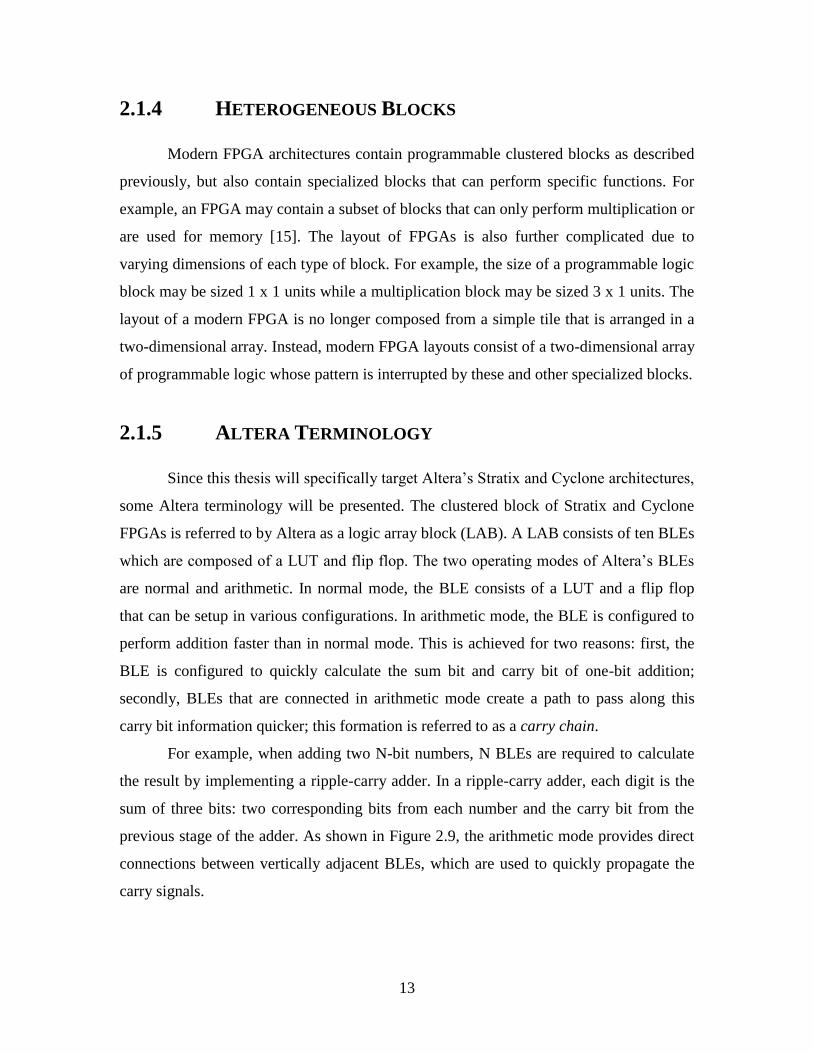
2.1.4 Heterogeneous Blocks ......................................................................... 13
2.1.5 Altera Terminology ............................................................................. 13
2.2 FPGA CAD Tools ........................................................................................... 15
2.2.1 Clustering ............................................................................................ 17
2.2.2 Placement ............................................................................................ 19
2.2.3 Routing ................................................................................................ 20
3 Dynamic Clusterer (DC) ............................................................................... 22
3.1 DC Overview .................................................................................................. 22
3.2 Configurable Design ....................................................................................... 24
3.3 Netlist Parser ................................................................................................... 24
3.4 Timing Analysis .............................................................................................. 25

TABLE OF CONTENTS
v
3.5 FPGA Architecture Model .............................................................................. 28
3.5.1 Sub-block Model ................................................................................. 28
3.5.2 Block Model ........................................................................................ 30
3.5.3 Clustered Block Model ........................................................................ 31
3.6 Clustering Constraint Language ..................................................................... 31
3.6.1 External and Internal Clustering Constraint Rules ............................ 32
3.6.2 If Rule .................................................................................................. 33
3.6.3 Max Rule ............................................................................................. 33
3.6.4 Split Rule ............................................................................................. 34
3.6.5 Pair Rule ............................................................................................. 35
3.6.6 Constraint Language Example ........................................................... 37
3.7 Clustering FPGA Architectural Language ...................................................... 38
3.7.1 Identity Rules ...................................................................................... 38
3.7.2 Unconnected Port Rules ..................................................................... 39
3.7.3 Sub-block Information ........................................................................ 40
3.7.4 Block Information ............................................................................... 41
3.7.5 Clustered Block Information ............................................................... 41
3.8 Carry Chain Implementation ........................................................................... 43
3.9 Changes Made to T-VPack ............................................................................. 45
3.10 Capabilities of The DC Tool ........................................................................... 47
3.10.1 Clustering Capability .......................................................................... 47
3.10.2 Clustering Limitation .......................................................................... 48
3.10.3 Clustering Future Work ...................................................................... 49
4 Dynamic Placer (DP) .................................................................................... 53
4.1 DP Overview ................................................................................................... 53
4.2 C onfigurable Design ...................................................................................... 55
4.3 FPGA Architecture Model .............................................................................. 55

TABLE OF CONTENTS
vi
4.3.1 Sub-block Model ................................................................................. 56
4.3.2 Block Model ........................................................................................ 58
4.4 Timing Analysis .............................................................................................. 58
4.4.1 Inter-Cell Delays ................................................................................. 59
4.4.2 Intra-Cell Delays ................................................................................ 60
4.5 Clustering Netlist (CNET) .............................................................................. 64
4.6 Placement FPGA Architecture Language ....................................................... 65
4.6.1 Sub-block Information ........................................................................ 66
4.6.2 Block Information ............................................................................... 66
4.7 Carry Chain Implementation ........................................................................... 67
4.8 Changes Made to VPR .................................................................................... 68
4.9 Capabilities of the DP Tool ............................................................................. 69
4.9.1 Placement Capability .......................................................................... 69
4.9.2 Placement Limitation .......................................................................... 71
4.9.3 Placement Future Work ...................................................................... 71
5 Experimental Methodologies ....................................................................... 73
5.1 Introduction ..................................................................................................... 73
5.2 FPGA Architecture Model .............................................................................. 73
5.3 Benchmark Set ................................................................................................ 74
5.4 Seed Sweeping ................................................................................................ 74
5.5 Test Flow ........................................................................................................ 76
5.5.1 The Quartus II Test Flow .................................................................... 76
5.5.2 The DC Test Flow ............................................................................... 76
5.5.3 The DP Test Flow ............................................................................... 77
5.6 Tool Settings ................................................................................................... 78
5.7 Metrics ............................................................................................................ 78
5.7.1 Maximum Frequency (Fmax) ................................................................ 78

TABLE OF CONTENTS
vii
5.7.2 Wire ..................................................................................................... 79
5.7.3 Runtime ............................................................................................... 79
6 Results ............................................................................................................ 80
6.1 Introduction ..................................................................................................... 80
6.2 DC and DP Results ......................................................................................... 80
6.2.1 Result Quality of DC versus Quartus II .............................................. 80
6.2.2 Result Quality of DP versus Quartus II .............................................. 83
6.2.3 Result Quality of DC and DP Tools versus Quartus II ....................... 83
6.3 Algorithm Experiments ................................................................................... 92
6.3.1 Experiment One: Investigate Clustering Carry Chains ...................... 93
6.3.2 Experiment Two: Spread-Out Clustering ........................................... 95
7 Conclusions and Future Work ..................................................................... 99
7.1 Contributions ................................................................................................... 99
7.2 Future Work .................................................................................................. 100
8 References .................................................................................................... 101
A CARCH File Syntax .................................................................................... 104
B CARCH File Examples ............................................................................... 108
B.1 CARCH File Used to Model Stratix Device ................................................. 108
B.2 CARCH File Used to Model Cyclone Device .............................................. 112
C Example of a CNET File ............................................................................. 116
D PARCH File Syntax .................................................................................... 118
E PARCH File Examples ............................................................................... 122
E.1 PARCH File Used to Model Stratix Device ................................................. 122
E.2 PARCH File Used to Model Cyclone Device ............................................... 128

TABLE OF CONTENTS
viii
F Tool Settings ................................................................................................ 133
F.1 DC Settings ................................................................................................... 133
F.2 DP Settings .................................................................................................... 133
F.3 Quartus II Settings ........................................................................................ 133

ix
LIST OF TABLES
Table 5.1: Specifications of the FPGA Architecture Modeled ......................................... 73
Table 5.2: Properties of Circuits in Benchmark Set ......................................................... 75
Table 6.1: Results from the DC Test Flow ........................................................................81
Table 6.2: DC Clustering Quality Compared to Quartus II .............................................. 82
Table 6.3: Results from the DP Test Flow ........................................................................ 84
Table 6.4: DP Placement Quality Compared to Quartus II .............................................. 85
Table 6.5: DC and DP Clustering and Placement Quality Compared to Quartus II ......... 87
Table 6.6: Comparing Clustering BLEs in Carry Chains in Isolation (Flow 1) versus
Clustering BLEs in Carry Chains with Other Logic (Flow 2) .................................. 94
Table 6.7: Parameter Values that were Investigated for Spread-Out Clustering .............. 96
Table 6.8: Results of Spread-Out Clustering Compared to Default Case ......................... 98

x
LIST OF FIGURES
Figure 2.1: FPGA Tile ........................................................................................................ 5
Figure 2.2: Programmable Switch ...................................................................................... 6
Figure 2.3: Example of a BLE ............................................................................................ 7
Figure 2.4: Example of a 2 Input LUT ............................................................................... 7
Figure 2.5: Example of a Clustered Block with Four BLEs ............................................... 8
Figure 2.6: Possible BLE Configurations ......................................................................... 10
Figure 2.7: Connection Block ........................................................................................... 11
Figure 2.8: Switch Block .................................................................................................. 12
Figure 2.9: Implementation of a Ripple-Carry Adder with BLEs .................................... 14
Figure 2.10: CAD Flow Process for FPGAs ..................................................................... 17
Figure 3.1: DC CAD Flow .................................................................................................22
Figure 3.2: An Example of a Circuit Timing Graph ......................................................... 27
Figure 3.3: Example of an FPGA Architectural Model for Clustering ............................. 29
Figure 3.4: Clustering Constraint Language Rules ........................................................... 32
Figure 3.5: An Example of how Subgroups are Created by the Split Rule ...................... 36
Figure 3.6: Example of Clustering Constraint Rules ........................................................ 37
Figure 3.7: Unconnected Port Rule ................................................................................... 40
Figure 3.8: Carry Chain Information ................................................................................ 43
Figure 3.9: Pseudo-code of the Modifications Made to T-VPack .................................... 46
Figure 3.10: Clustering Flow Required for Stratix II and Stratix III Architecture ........... 52
Figure 4.1: DP CAD Flow .................................................................................................53
Figure 4.2: Example of an FPGA Architecture Model for Placement .............................. 57
Figure 4.3: How a Registered Node is Modeled by the DP Tool ..................................... 61
Figure 4.4: Example of a Block Intra-Cell Timing Graph Model .................................... 63
Figure 4.5: Block to Sub-block Connection Model .......................................................... 64
Figure 4.6: Syntax of a CNET file .................................................................................... 65
Figure 4.7: Example of the Placement Required for a Carry Chain ................................. 68

xi
Figure 4.8: Pseudo-code of the Modifications Made to VPR ........................................... 70
Figure 5.1: Experimental Test Flow ..................................................................................77
Figure 6.1: Runtime of DC Tool Versus Number of BLEs in the Circuit .........................88
Figure 6.2: Runtime of DP Tool Versus Number of BLEs in the Circuit ........................ 89
Figure 6.3: Runtime of Quartus II Versus Number of BLEs in the Circuit ...................... 89
Figure 6.4: Fmax Achieved Versus Number of BLEs in the Circuit for the DC and DP
Tools ......................................................................................................................... 90
Figure 6.5: Fmax Achieved Versus Number of BLEs in the Circuit for Quartus II CAD
Software .................................................................................................................... 91
Figure 6.6: Amount of Wire Required Versus Number of BLEs in the Circuit for the DC
and DP Tools............................................................................................................. 91
Figure 6.7: Amount of Wire Required Versus Number of BLEs in the Circuit for Quartus
II CAD Software ....................................................................................................... 92
Figure 6.8: Fmax Improvement Across Different Values of MIN_GAIN for each Value of
MIN_SIZE Investigated ............................................................................................ 98

xii
LIST OF ACRONYMS
ALM ................................................................................................ Adaptive Logic Module
BLE ...................................................................................................... Basic Logic Element
BLIF ............................................................................. Berkeley Logic Interchange Format
CAD ............................................................................................... Computer Aided Design
CARCH ................................................................................. Clustering FPGA Architecture
CNET ........................................................................................................ Clustering Netlist
CTCL ................................................................................................. Clustering TCL script
DC ........................................................................................................... Dynamic Clusterer
DP ................................................................................................................ Dynamic Placer
DSP ............................................................................................... Digital Signal Processing
FPGA .................................................................................Field-Programmable Gate Array
HDL .................................................................................. Hardware Description Language
LAB......................................................................................................... Logic Array Block
LUT ................................................................................................................. Lookup Table
PARCH ................................................................................. Placement FPGA Architecture
PLDM ....................................................................................................Placer Delay Model
PTCL .................................................................................................. Placement TCL script
RAM ............................................................................................. Random Access Memory
SRAM ................................................................................. Static Random Access Memory
TCL .............................................................................................. Tool Command Language
VPR .............................................................................................. Versatile Place and Route
VQM ............................................................................................ Verilog Quartus Mapping

1
1 INTRODUCTION
1.1 OVERVIEW OF FPGAS
Field-Programmable Gate Arrays (FPGAs) have become a viable method to
implement digital circuits due to their increasing gate densities and performance [1].
FPGAs allow for a faster time to market than other circuit implementations because they
can easily be configured to implement any circuit [2]. This fast time to market has led to
the use of FPGAs in multiple phases of a product design cycle including production use,
pre-production use, prototyping, and emulation [1].
The performance of an FPGA is dependent on its architecture including the design
of its logic block and its interconnection fabric. Also, the ability to effectively configure
the FPGA is highly dependent on computer aided design (CAD) tools that are used to
implement the circuit [2]. For this reason FPGA CAD tools are usually developed in
synchronization with FPGA architectures [1]. The ability of these CAD tools to meet the
designer’s speed and area requirements is critical to the continued success of FPGAs.
1.2 MOTIVATION
Historically, academic FPGA CAD tools have been developed and used to study
FPGA design in many research projects [3][4][5][6][7]. In order to fairly judge the results
of new FPGA architectural features and CAD tool algorithms, a tool that is able to model
a wide variety of architectures, and achieve a high quality is required. FPGA CAD tools
that have been developed in the academic field have previously provided a good
foundation to determine the usefulness of various FPGA design architectures [2][3].
However, the FPGA architecture that is modeled by these tools is not sufficiently
complex enough to capture the features of a modern FPGA.

2
Early FPGAs were homogeneous in their structure and consisted of an array of
programmable logic blocks that could be connected by programmable routing switches.
Along the perimeter of the FPGAs are input and output (I/O) pads that are used to
connect the implemented circuit’s I/O pins to external devices [8][9]. Modern FPGA
architectures are more complex and are heterogeneous in nature; they contain both an
array of programmable logic blocks and other types of specialized blocks. These
specialized blocks can perform specific functions such as multiplication or storage and
are located at specific locations within the two-dimensional array of programmable logic
blocks on the FPGA chip [8][9].
Two of the most widely used FPGA CAD tools in academia are T-VPack and
Versatile Place and Route (VPR). An issue with these tools is they cannot target modern
FPGA architectures because they support only homogeneous FPGA architectures. The
purpose of this research thesis is to upgrade these tools so that they can model more
complex FPGA architectures. This thesis describes two new tools, the Dynamic Clusterer
(DC) and the Dynamic Placer (DP). These tools have been designed to be flexible enough
to target a wide variety of new architectures and provide performance capabilities
comparable to commercial FPGA CAD software. The code will be available for
download to aid future academic FPGA architecture and CAD tool studies. By expanding
the model of the target FPGA used by academic researchers, the results obtained will be
more relevant to the latest technology used in industry.
DC and DP are based on T-VPack and VPR respectively. T-VPack is responsible
for grouping basic logic elements (BLEs) into larger blocks, which is a process referred
to as clustering. T-VPack’s code has been modified to create the DC tool. The VPR tool
is responsible for placing each clustered block into the FPGA array, and routing the
connections between the blocks. VPR’s code is used as a base for creating the DP tool.
This thesis will discuss the design of these tools which are able to target current FPGA
architectures found in commercial FPGAs; specifically Altera’s Stratix and Cyclone
architectures are targeted to illustrate the capability of the DC and DP tools.

3
1.3 KEY OBJECTIVES
The objective of this thesis is to adapt the T-VPack and VPR tools to be able to
study a wider range of FPGA architectures, including modern FPGA architectures, in an
academic environment. In particular, these tools will be adapted to be able to target any
style of FPGA architecture, including those found in Altera’s Stratix and Cyclone
families. This thesis will expand these tool’s current ability to perform clustering and
placement.
In working towards the objective, an updated clustering tool must be designed that
will be able to group together different blocks without breaking any of the legality
constraint rules of a clustered block. For example, the present ability of T-VPack only
checks the following two legality constraints: 1), the maximum number of inputs of a
clustered block and 2), the maximum number of clock inputs of a clustered block. These
constraints were the only ones needed for early FPGA architectures. However, modern
commercial FPGAs entail many more types of constraints, and are particularly complex
in the constraints that are required for various control signals within a clustered block
[10]. Furthermore, the placer tool has to determine the position of blocks in the FPGA to
meet speed and routing requirements. VPR’s present ability can only address
homogenous FPGAs which do not have any specialized blocks.
The new clustering and placement tools have been designed to be flexible enough
to model a wide variety of FPGA architectures by simply changing an input file, the
FPGA architecture specification file, to the programs. Furthermore, for the DC and DP
tools to have merit in future academic studies they must be able to achieve a performance
quality comparable to commercial tools.
To achieve the flexibility that is required, the DC and DP tools are designed to be
configurable which enables the tools to model future FPGA architectures without any
major changes to the code. The code and the complete testing infrastructure will be
available for future academic studies of FPGA architectures and FPGA CAD tools.

4
1.4 ORGANIZATION
This thesis is organized as follows: Chapter 2 provides a review of recent FPGA
architectures and the main challenges in FPGA CAD tools. The chapter also includes a
review of current academic CAD tools and their limitations to model modern FPGA
architectures. Chapter 3 describes the design implementation of the DC tool. Specifically,
this chapter will describe the details of updating the clustering of T-VPack. Chapter 4
describes the design implementation of the DP tool. This chapter will describe the details
of updating the placement functionality of VPR. Chapter 5 describes the testing
infrastructure used to analyze the performance of the new CAD tools including the
benchmarks used. Chapter 6 presents the results of experiments that measure the quality
of the DC and DP tools; these results are compared with real commercial FPGA CAD
software. Finally, Chapter 7 provides a summary of this thesis along with future
modifications and studies for the updated programs.

5
2 BACKGROUND
2.1 FPGA ARCHITECTURE
Early FPGA architectures were homogeneous in their structure and consisted of a
tile that is repeatedly laid out in a two-dimensional array [11]. The tile consists of one
logic block, two connection blocks, and a switch block that is laid out as seen in Figure
2.1. I/O pads are located on the perimeter of the FPGA to connect the implemented
circuit to external devices.
Figure 2.1: FPGA Tile
A circuit is implemented in an FPGA by configuring the logic blocks to capture
the behaviour of the circuit and route the connections of the circuit using the routing wire
segments [2]. The most popular method used to make an FPGA programmable is by
using SRAM cells to control programmable switches [2].
Earlier technology used pass transistors to implement a programmable switch. A
transistor is a three terminal device with a gate terminal, source terminal, and drain
terminal [12]. A transistor can be made into a programmable switch, or pass transistor, by
L – Logic Block
C – Connection Block
S – Switch Block
L C
C S
L C
C S
L C
C S
L C
C S
L
C
L
C
L C L C L
One Tile Block

6
connecting an SRAM cell to its gate terminal. Whenever the gate terminal of the pass
transistor is connected to a signal with the logic value one, a connection is made between
the other two terminals. Conversely, a pass transistor can be turned off by assigning the
logic value zero into the SRAM cell. Thus, the SRAM cell value controls the state of the
pass transistor [12]. The value of the SRAM cell is programmed by FPGA CAD tools.
Modern FPGAs implement programmable switches using direct drive
multiplexers. An N-to-1 multiplexer is a logic function that selects one of its N inputs to
connect to its one output. A direct drive multiplexer uses a buffer to drive the output of
the multiplexer as seen in Figure 2.2. Usually multiplexers are constructed using pass
transistor logic, and SRAM cells control the selection of the input as seen in Figure 2.2. A
buffer at the multiplexer output drives the associated interconnection wire. The value of
the SRAM cells is programmed by the FPGA CAD tools.
Figure 2.2: Programmable Switch
Switch Output Switch Inputs Buffer
SRAM Cells
. . .
N – 1
Multiplexer
.
.
.
input n
input n – 1
input 3
input 2
input 1

7
2.1.1 LOGIC BLOCK
A logic block is made up of a group of basic logic elements (BLEs) and is also
referred to as a clustered block. A BLE consists of a k-input lookup table (LUT) and a
flip flop as seen in Figure 2.3. A LUT contains a number of programmable SRAM cells
that are used to store a logic function. Figure 2.4 shows a model of a two-input LUT
which can implement any function of two inputs by programming the four SRAM cells
accordingly. Similarly, a k-input LUT can implement any logic function with k number
of inputs [2]. The functionality of a digital circuit can be implemented by a collection of
BLEs by allowing each BLE to capture a portion of the behaviour of the circuit.
Therefore, any digital circuit can be implemented in an FPGA as long as it contains
enough BLEs and routing resources.
Figure 2.3: Example of a BLE
Figure 2.4: Example of a 2 Input LUT
2 LUT
Inputs 4 – 1 Multiplexer
LUT Output
4 SRAM Cells
LUT
Flip
Flop BLE
Inputs
BLE
Output

8
The presence of a clustered block creates a two level hierarchy of routing
resources available on an FPGA. The first level of routing resources consists of the
connections within a clustered block. Routing connections are present within a clustered
block to allow outputs of BLEs to feed into inputs of other BLEs [13]. Figure 2.5 shows
an example of a clustered block that has four BLEs and wires to interconnect them. The
second level of routing resources in an FPGA consists of the connections between
clustered blocks which consist of horizontal and vertical routing channels. These
resources are used to connect one clustered block to another, and to connect the clustered
blocks to the FPGA’s I/O pins.
Figure 2.5: Example of a Clustered Block with Four BLEs
BLE
BLE
BLE
BLE
Clock
I
N
N
Cluster
Outputs
I
Cluster
Inputs

9
Logic blocks in modern FPGA architectures are more sophisticated than the
earlier ones. BLEs now contain LUTs with different sizes, more modes of operations, and
contain extra functionality. Each will be discussed in more detail in the next few sections.
LUT SIZES
Early FPGA architectures mainly consisted of only one type of LUT. Previous
research had shown that a four-input LUT provided FPGAs with the highest area
efficiency [2][14]. However, modern FPGA architectures now support the
implementation of LUTs of different sizes. Altera’s Stratix II family can be configured as
one 6 LUT or two LUTs with five or fewer inputs [15][16].
BLE MODES OF OPERATION
In traditional academic work, BLEs were designed to operate in only one mode,
consisting of a LUT that could feed its output into a flip flop. In modern FPGA
architectures, BLEs are more complex in that they support a variety of operating modes.
BLEs can now operate as described before with a LUT and a flip flop, but also can be
configured to speed up addition [13][15]. The LUT and flip flop configuration itself can
also be setup in various modes within the BLE to accommodate the best circuit
implementation for speed and area. Figure 2.6 demonstrates a BLE configured in normal
mode and arithmetic mode. In normal mode, a simple LUT and flip flop is provided. In
arithmetic mode, the LUT is divided into two parts to efficiently calculate the sum bit and
carry bit for addition as seen in Figure 2.6.

10
Figure 2.6: Possible BLE Configurations
BLE FUNCTIONALITY
Early FPGA architectures contained only LUT inputs and clock signals as
possible inputs to a BLE. In modern FPGA architectures, BLEs include a number of other
types of inputs such as various types of control signals for flip flops and special types of
fast connections for linking BLEs together in specific ways [15]. These various types of
inputs complicates the clustering process as discussed in Section 2.2.1.
LUT
Flip
Flop
BLE
Inputs
BLE
Output
Configuration 1: Normal Mode
LUT Flip
Flop BLE
Inputs
Sum
Bit
Configuration 2: Arithmetic Mode
LUT Carry
Bit

11
2.1.2 CONNECTION BLOCK
A connection block connects the inputs and outputs of the logic block to the
horizontal and vertical routing channels as seen in Figure 2.7. Each logic block’s I/O may
connect to all of the wire segments in the connection block or only to a certain percentage
of the wire segments in the connection block. The percentage of wires each logic block’s
I/O can connect to depends on the connectivity design of the FPGA [2]. Programmable
switches are used to setup the configuration of the connection block. In modern FPGA
architectures, programmable switches are implemented using multiplexers as seen in
Figure 2.2 [13]. The inputs of a multiplexer in a programmable switch are connected to
the outputs of clustered blocks and other wire segments in the routing channel. The
output of the multiplexer drives one of the wire segments in the routing channel. SRAM
cells are used to determine which switch input should drive the wire segment as seen in
Figure 2.2.
Figure 2.7: Connection Block
Logic
Block
Connection
Block
Vertical
Routing
Channels
Connection
Block
Connection
Block
Horizontal
Routing
Channels
Connection
Block

12
2.1.3 SWITCH BLOCK
A switch block is present wherever a horizontal and vertical routing channel
intersects [2]. The switch block allows wire segments in one routing channel to connect
to wire segments in another routing channel. The connections in the switch block are
controlled by the programmable switches as seen in Figure 2.2 [17]. Figure 2.8 shows an
example of one possible configuration of a switch block. Each wire incident to the switch
block may connect to all or a certain percentage of the other wire segments depending on
the switch block design of the FPGA.
FPGAs have a certain percentage of wire segments in each routing channel of
different lengths [2]. The longer length wire segments are used to improve the speed of
connections between clustered blocks that are located a great distance apart on the FPGA.
The performance of FPGAs with longer wire segments improves because fewer number
of switches are required to route a connection along a path; that is, longer length wire
segments pass through some of the switch blocks unbroken and do not require a switch.
A switch decreases the performance of a connection because of the propagation time
through the switch [2].
Figure 2.8: Switch Block
Connectivity determine by
programmable switches
Switch Block
Vertical
Routing
Channel
Horizontal
Routing
Channel
13
2.1.4 HETEROGENEOUS BLOCKS
Modern FPGA architectures contain programmable clustered blocks as described
previously, but also contain specialized blocks that can perform specific functions. For
example, an FPGA may contain a subset of blocks that can only perform multiplication or
are used for memory [15]. The layout of FPGAs is also further complicated due to
varying dimensions of each type of block. For example, the size of a programmable logic
block may be sized 1 x 1 units while a multiplication block may be sized 3 x 1 units. The
layout of a modern FPGA is no longer composed from a simple tile that is arranged in a
two-dimensional array. Instead, modern FPGA layouts consist of a two-dimensional array
of programmable logic whose pattern is interrupted by these and other specialized blocks.
2.1.5 ALTERA TERMINOLOGY
Since this thesis will specifically target Altera’s Stratix and Cyclone architectures,
some Altera terminology will be presented. The clustered block of Stratix and Cyclone
FPGAs is referred to by Altera as a logic array block (LAB). A LAB consists of ten BLEs
which are composed of a LUT and flip flop. The two operating modes of Altera’s BLEs
are normal and arithmetic. In normal mode, the BLE consists of a LUT and a flip flop
that can be setup in various configurations. In arithmetic mode, the BLE is configured to
perform addition faster than in normal mode. This is achieved for two reasons: first, the
BLE is configured to quickly calculate the sum bit and carry bit of one-bit addition;
secondly, BLEs that are connected in arithmetic mode create a path to pass along this
carry bit information quicker; this formation is referred to as a carry chain.
For example, when adding two N-bit numbers, N BLEs are required to calculate
the result by implementing a ripple-carry adder. In a ripple-carry adder, each digit is the
sum of three bits: two corresponding bits from each number and the carry bit from the
previous stage of the adder. As shown in Figure 2.9, the arithmetic mode provides direct
connections between vertically adjacent BLEs, which are used to quickly propagate the
carry signals.
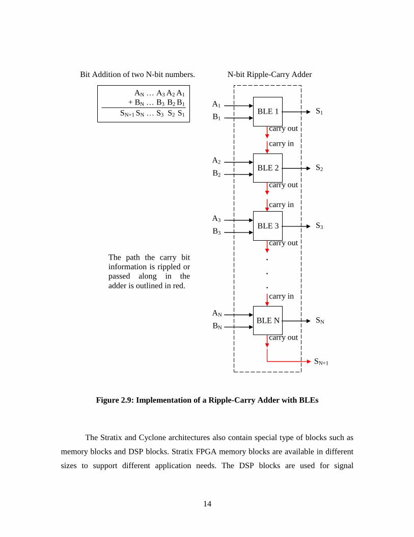
14
Figure 2.9: Implementation of a Ripple-Carry Adder with BLEs
The Stratix and Cyclone architectures also contain special type of blocks such as
memory blocks and DSP blocks. Stratix FPGA memory blocks are available in different
sizes to support different application needs. The DSP blocks are used for signal
AN … A3 A2 A1
+ BN … B3 B2 B1
SN+1 SN … S3 S2 S1 BLE 1 A1
B1
carry out
S1
BLE 2 A2
B2
carry in
carry out
S2
BLE 3 A3
B3
carry in
carry out
S3
BLE N AN
BN
carry in
carry out
SN
.
.
.
SN+1
Bit Addition of two N-bit numbers. N-bit Ripple-Carry Adder
The path the carry bit
information is rippled or
passed along in the
adder is outlined in red.
15
processing applications and can perform various addition and multiplication functions
faster than they can be performed in logic blocks.
The Stratix and Cyclone FPGAs contain two hierarchical levels of routing
resources [2][13]. The first level consists of the local connections of the inputs and
outputs of the BLEs in the LAB. The second level of routing resources consists of the
collection of horizontally and vertically routing channels that surround the LABs. The
horizontal channels of the Stratix FPGA contain approximately twice as much routing
resources than the vertical channels [15]. The Stratix FPGA requires more horizontal
routing resources since the horizontal channels are in more demand than the vertical
channels, which is due to the length of the LAB being much longer than its width [13].
The Stratix and Cyclone routing architecture design requires FPGA CAD tools to
effectively group together BLEs into clustered blocks. This is necessary since the delay
between two BLEs within the same clustered block is shorter than the delay between two
BLEs in different clustered blocks.
2.2 FPGA CAD TOOLS
Hardware designers develop digital circuits using a hardware description language
(HDL) to describe the circuit and CAD tools then translate it into the resources available
on the FPGA chip. The CAD tools’ objective in this process is to map the circuit onto the
FPGA to meet the user’s area and speed requirements. The CAD flow involves five major
steps of optimization: synthesis, technology mapping, clustering, placement, and routing
as shown in Figure 2.10.
The HDL code is first synthesized into basic gates and is logically optimized to
ensure the code is efficient by removing redundant logic and simplifying the logic
functions. In the second step of the CAD flow, the basic gates are then technology
mapped into logic blocks on the FPGA, usually LUTs and flip flops; the basic gates are
translated into logic blocks such that the number of blocks is minimized and/or the speed
of the circuit is maximized [2].
The next step is clustering, which is a two step process; in the first step LUTs and
flip flops are packed into BLEs and in the second step, BLEs are grouped together into a

16
clustered block that is optimized for circuit speed, area, and/or routability. The clustering
problem is similar to a classic optimization problem, partitioning. This involves
determining how to divide a number of blocks into different groups [2]. The method used
in T-VPack is discussed in Section 2.2.1.
After clustering is completed, the next step in the CAD flow requires the placer to
determine where to position the clustered blocks in the FPGA. The clustered blocks are
placed to either maximize circuit speed, routability, or minimize the wire length used [2].
Many types of algorithms have been used in the literature to perform placement. Some
popular techniques include min-cut [18][19], analytic [20][21], and simulated annealing
placers [22][23]. VPR uses a simulated annealing algorithm which is discussed in more
detail in Section 2.2.2.
Once clustered blocks have been placed, a router determines how to route the
connections between blocks to complete the circuit. The router finds a path in the FPGA
routing resources by determining which programmable switches need to be turned on in
the FPGA [2].
As mentioned in Chapter 1, the purpose of this thesis is to create CAD tools that
perform the clustering and placement steps of the CAD flow process in Figure 2.10. The
DC tool developed will perform the clustering step described in the FPGA CAD flow
process. The output of the DC tool is then fed into the DP tool which will determine the
placement of the clustered blocks of the circuit into the FPGA. In this thesis, Altera’s
industrial CAD software tool, Quartus II, will be used to perform the steps before
clustering, and after placement. This will allow a direct comparison of the DC and DP
tools to Altera’s Quartus II CAD software.
17
Figure 2.10: CAD Flow Process for FPGAs
2.2.1 CLUSTERING
Clustering is the process of packing BLEs into larger clustered blocks. A BLE
consists of a LUT and a flip flop. T-VPack takes as input a netlist of LUTs and flip flops
and outputs a netlist of logic clusters. A clustered block can contain N BLEs and local
routing to interconnect them [2][3][14]. Clustering is a critical step in the process to
achieve the speed requirements of the circuit. This is because the delay of the connections
between two BLEs within a clustered block is smaller than the delay of the connections
between two BLEs from two different clustered blocks. The decision of which BLEs to
Circuit Description (HDL)
Synthesis
Technology mapping
Clustering
Placement
Routing
FPGA Programming file
18
group together will affect the maximum frequency (Fmax) of the circuit. Fmax is the
maximum frequency or speed at which the clock in the circuit can be set and still
maintain the desired behaviour of the circuit. The speed of the clock is determined by the
longest register to register path where both registers use the same clock. The Fmax of a
circuit is an important metric used to compare the quality of FPGA CAD tools [15].
T-VPack attempts to achieve the highest possible Fmax by trying to minimize the number
of connections between clusters on the critical path [2][3]. The critical path is the path on
the circuit with the longest delay. Optimizing the critical path is important because
increasing the delay on any connection along the critical path would decrease the Fmax of
the circuit.
The current structure of a clustered block that T-VPack uses consists of a two
level hierarchy. A clustered block is a collection of BLEs grouped together and a BLE is
made up of a LUT and a flip flop. The clustered block can contain N BLEs and local
routing to interconnect them. The user can specify the number of BLEs in a clustered
block, number of inputs to a LUT, number of inputs to the clustered block, and the
number of clock inputs for use by the flip flops [10]. T-VPack ensures that each cluster
does not violate any of the restrictions imposed by the user. The program creates the
clusters in two stages; first it packs the LUTs and flip flops together into BLEs and then it
packs multiple BLEs into clustered blocks.
T-VPack uses an optimal pattern matching algorithm to pack a flip flop and a
LUT into a BLE [2][3]. In T-VPack’s algorithm, when the output of a LUT fans out to
only a single flip flop, both LUT and flip flop can be packed in a single BLE. Otherwise,
T-VPack packs the LUT and flip flop into two separate BLEs.
Depending on what the user wishes to accomplish, the algorithm used to fill each
clustered block to its capacity will attempt to minimize the routing requirements of the
circuit and/or delay of the circuit. T-VPack constructs each clustered block in two phases.
First, the algorithm greedily packs BLEs into a cluster by choosing a seed BLE based on
some criteria depending on what the user is trying to optimize. The tool allows the user to
optimize for routing and/or circuit speed. It will then select the BLE with the highest
attraction, which is a function that is dependent on what the user is trying to optimize, to
the current cluster. The algorithm is continued until the current cluster is full or adding

19
any remaining BLE would make the current clustered block illegal [2][3]. If a clustered
block is not full, the second part of algorithm, which is the hill climbing section, is
initiated. In the hill climbing section, T-VPack allows a BLE to be add to the clustered
block even if it makes the clustered block fail a legality constraint; this is done with the
hope that adding additional BLEs to the clustered block will make the clustered block
feasible again [2][3]. However, the only legality constraint that T-VPack allows the
clustered block to fail during the hill climbing phase is the maximum number of clustered
block inputs. The hill climbing phase ends when the clustered block is full; at this point if
the clustered block still breaks a constraint, the clustered block is returned to the state
when it was last valid.
The only constraints the user can specify in T-VPack are the number of clock
inputs to a cluster and the total number of inputs that can be routed into a cluster [10].
The T-VPack tool has been modified in this thesis to include the ability to check legality
constraints that are needed for modern FPGA architectures. This thesis will also add to
T-VPack the ability to cluster carry chains.
2.2.2 PLACEMENT
Placement determines which block within an FPGA should implement each of the
clustered blocks required by the circuit. The algorithm to implement placement tries to
optimize either wire length, routability across the FPGA, or maximize the circuit speed.
The placement algorithm must attempt to use all of the features of an FPGA, and allow
the optimization goals of the placer to change from architecture to architecture. Currently
there are three types of placers used: min-cut, analytic, and simulated annealing placers.
The VPR tool uses a simulated annealing placer which mimics the annealing
process used to gradually cool molten metal to produce high-quality metal
objects [2][24]. The initial placement is created by assigning clustered blocks randomly
to the available locations in the FPGA. A large number of moves are then made to
gradually improve the placement. A cost function is used to determine whether each
move is accepted. Even moves that make the placement worse have a probability of being
accepted; these hill climbing moves allows the simulated annealing to escape local

20
minima in the cost function. The program uses an adaptive annealing schedule based on
statistics computed during the anneal itself [2][24].
To be able to target a wide variety of FPGA architectures, the VPR tool models
the architecture as a set of discrete locations at which clustered blocks or I/O pads can be
placed. The user can specify architecture options in the architecture description file to
model the FPGA [10]. There are two main limitations that exist in the VPR tool that
prevents it from targeting modern FPGA architectures. The first limitation is the user can
only specify two types of blocks, clustered blocks and I/O pads. The second issue is that
there are limitations in what kind of floorplan the user can specify in terms of block
placement and the size of the blocks on the FPGA. In this thesis, the VPR tool will be
modified to model new types of blocks that are present in modern FPGA architectures
and be able to incorporate a wider range of FPGA floorplans. These changes will allow
the DP tool to model a wider range of FPGA architectures.
2.2.3 ROUTING
The routing problem for an FPGA results in a different set of issues than the
traditional routing problem for a non programmable chip. Connections in an FPGA are
made by turning on or off various switches to connect wire segments that are already
placed at fixed locations in the FPGA. The key problem that arises when routing an
FPGA is that a connection made for one net in the circuit might block another net in the
circuit from being able to be routed on the FPGA [11]. The routing algorithm must be
aware of congestion in each routing channel to ensure all connections can be routed.
VPR also has the capability to perform routing, and uses a PathFinder negotiated
congestion algorithm to route the connections [2][4][24]. The PathFinder algorithm
solves the congestion problem by iteratively re-routing connections until all nets can be
routed. The router operates on the directed graph that models the FPGA routing
resources. VPR is designed to take a human-comprehensible architecture definition file
and uses an internal graph generator to create the highly detailed routing-resource graph
representation [2][4][24]. The routing-resource graph representation can describe a wide
variety of FPGA architectures. Thus, to make VPR compatible with newer FPGA
21
architectures, only the routing graph generator needs to be modified. The router, graphics,
timing analyzer, and statistics routines will all function correctly.
Currently, the DP tool does not perform routing. The source code to the DP tool
will be made available for future academic research studies to expand the functionality of
the DP tool to perform routing. VPR’s routing code information is made available in the
DP tool.

22
3 DYNAMIC CLUSTERER (DC)
3.1 DC OVERVIEW
The DC tool performs clustering of BLEs for modern FPGA architectures. Figure 3.1
demonstrates the CAD flow that is used with the DC tool. The circuit description file is
synthesized and technology mapped by the Quartus II synthesis tool, quartus_map, and
the resulting circuit description is output, in netlist format, to a Verilog Quartus Mapping
(VQM) file. The FPGA architecture that is modeled by the DC tool is described using the
Clustering FPGA Architecture (CARCH) language specified in the CARCH file. The DC
tool reads in the circuit information from the VQM file and the architecture information
from the CARCH file and performs the clustering step in the FPGA CAD flow process as
described in Section 2.2.1.
Figure 3.1: DC CAD Flow
Quartus II (quartus_fit)
CTCL file
Dynamic Clusterer (DC)
CARCH file
Circuit Description
Quartus II (quartus_map)
VQM file
CNET file
Dynamic Placer (DP)

23
Currently the DC tool only contains a VQM parser to read in the circuit netlist but
can easily be expanded to include other languages as described in Section 3.3. The DC
tool outputs the clustering results to two files, the CNET file and the CTCL file. The
CNET file describes the clustering results of the circuit that can be read in by the DP tool
to perform the placement step in the CAD flow as shown in Figure 3.1. The CTCL file is
a TCL script file that stores the clustering results via assignment statements that can be
imported into Altera’s Quartus II CAD software. Importing the clustering results into
Altera’s Quartus II CAD software provides a way to measure the quality of the clustering
results of the DC tool as described in Chapter 5.
DC is designed to be a dynamic tool because it can model a wide variety of FPGA
architectures. The flexibility of the DC tool was accomplished by modifying the code of
T-VPack to be configurable. Designing a configurable clustering tool first requires
developing multiple interface languages that are required to describe various architectural
features of an FPGA device and algorithm features of FPGA CAD tools. T-VPack cannot
model modern FPGA architectures due to the limitations that were described in Section
2.2.1. The clustering algorithms used in T-VPack need to be modified to handle the
configurable design.
A configurable clustering tool is able to model a wide range of FPGA architectures
without any modifications to the algorithms within the tool. A specific FPGA architecture
design will require algorithms within the clustering tool to adapt to meet the needs of the
new FPGA design. For example, changing the architectural design of a clustered block
will impact several algorithms within the clusterer. One algorithm that is greatly affected
by the design of the clustered block is the cluster constraint rule checking algorithm. The
cluster constraint checker ensures that each clustered block can be legally grouped
together. Altering the architecture of the clustered block will directly impact the rules
used by the cluster legality rule checker algorithm to check if a cluster block is legal as
described in Section 3.6. The DC tool is able to model a wide range of architectures
because of its configurable design allows the user to specify all the architecture
information of an FPGA and the behaviour of the clustering algorithms from a file.

24
The changes that were made in T-VPack to create the DC tool are listed below:
Updated the clustering and timing algorithms to be configurable
Added a parser that could parse a modern HDL language
Updated the timing analysis model
Developed a new method to model the architecture of an FPGA
Created a clustering constraint language
Created an FPGA architectural specification language
Added new functionality: the ability to cluster carry chains.
The rest of this chapter will describe the implementation details and the capabilities of the
DC tool.
3.2 CONFIGURABLE DESIGN
The DC tool was designed to be configurable by using general data structures to
store specific FPGA architectural and clustering information. These data structures are
then accessed by the algorithms used in the DC tool to retrieve any FPGA architecture or
algorithm information. The algorithms within the DC tool were adapted to operate on any
type of FPGA architecture the tool is able to model. The flexibility of the configurable
design was achieved by implementing a dynamic Clustering Architectural (CARCH)
description language which allows the user to specify a wide range of FPGA
architectures. The information specified with the CARCH language populates the general
data structures which are used by the algorithms of the DC tool.
The CARCH file is used to provide information regarding the FPGA architecture
to model, and the clustering constraint rules to follow for the clustering step in the FPGA
CAD flow. The versatility of the clustering constraint rules the user can specify and
CARCH language is described in more detail in Sections 3.6 and 3.7 respectively.
3.3 NETLIST PARSER
The DC tool requires a parser that can read in a circuit description language that
uses complex block types seen in modern FPGA architectures. The T-VPack tool used a
set of circuits described by Berkeley Logic Interchange Format (BLIF) files that only
contained simple block types. A more full featured language was needed to be able to
describe more complex designs and block types which would be able to test the complete
functionality of the DC tool. The language that was chosen to describe circuit designs

25
was VQM. Presently, VQM netlists is the only file format that can be used with the DC
tool.
VQM files are generated by Altera’s Quartus II CAD software that can take any
HDL description language as input. The VQM file describes the circuit using the block
types that are present from the Quartus II device the user selects when generating the
VQM. The block types used by Quartus II devices are more complex than block types
described by BLIF files. The complexity of the block types that can be described by
VQMs is illustrated by the large amount of mode information that is associated with each
block type in the design. The mode information is required to define the behaviour of
each block since each block type may have several different configurations.
The DC tool presently interfaces with a parser created by Czajkowski [25] which
is capable of parsing a VQM file and storing the information in a set of data structures.
The DC tool’s simply interfaces with this parser to populate internal general data
structures of the DC tool with the circuit information.
To use a different netlist language as input to the DC tool would only require
implementing a parser to read in the new language. The parser would be required to read
in the information describing the circuit and load the internal data structure of the DC tool
with the circuit description information. Implementing a new HDL language parser
would require no other changes to any of the internal algorithms to support the different
circuit description language. The algorithms used in the DC tool are configurable and
only interact with the internal data structures to obtain circuit information.
3.4 TIMING ANALYSIS
A timing analysis model is required to perform timing driven clustering. Timing
driven clustering groups together basic logic elements (BLEs), which was introduced in
Chapter 2, in a way to maximize the performance, Fmax. The Fmax of the circuit, recall
from Chapter 2, is the longest register to register path where both registers use the same
clock. The DC tool’s timing analysis works by modeling the circuit as a graph of
connected nodes that represents all the connections in the circuit. Any connected output
port on the block in the netlist is considered a node in the timing graph. A path in the
timing graph is a set of node connections in the circuit. A source node is any node that

26
begins the start of a path in the circuit and is usually either a registered output of a block
or input pin of the circuit. A sink node is any node that ends a path and is usually a
registered output of a block or output pin of a circuit. A path must then start at a source
node and end at a sink node. The longest paths in the timing graph are considered critical
paths since minimizing these paths will increase the Fmax of the circuit. Timing driven
clustering is performed by identifying the critical paths in the circuit and attempting to
cluster the circuit to minimize the delays of these paths.
T-VPack assumed blocks only contained one output port so the number of nodes
in the timing graph and the number of blocks in the circuit netlist had a 1-1 relationship.
The 1-1 block to node relationship allowed timing analysis in T-VPack to identify each
block in the circuit as one node. This design methodology only works for block types
with one output, whereas the DC tool supports block types which could have multiple
registered and combinational outputs.
The solution used by the DC tool is to model each output of each block in the
netlist as a separate node in the timing graph as illustrated in Figure 3.2. The figure
displays a small example illustrating how the timing graph is created for the circuit.
Figure 3.2a displays the sample circuit used and Figure 3.2b displays the corresponding
timing graph created for the circuit. Block 5, which has both a combinational and
registered output, becomes two nodes in the timing graph.

27
Figure 3.2: An Example of a Circuit Timing Graph
5
C
Input
pin
Input
pin
R
C
C C
Output
pin
C
R
C
C
a) Circuit Netlist
b) Timing Graph
1
2
3
4
5
6 8
7 9
10
0
11
0
1
2
3
4
6
7
8
R – Registered Output
C – Combinational Output
Source Node
Sink Node
Source & Sink Node
Node
9
10
0
11
0

28
3.5 FPGA ARCHITECTURE MODEL
The DC tool must model an FPGA architecture to meet two objectives: one,
model a wide range of architectures; and two, support clustering of the circuit for the
chosen architecture model. The FPGA features that need to be modelled are shown in
Figure 3.3. At the lowest level we need to model an element such as a LUT and a flip
flop; such elements are referred to as sub-blocks in the model. At the next level we need
to model elements such as BLEs, RAM blocks, or similar resources; these are referred to
as blocks in the model. Finally, we need to model groups of blocks, which are called
clustered blocks in the model.
The FPGA architecture model can be specified using the Clustering Architecture
(CARCH) specification language. The CARCH language allows the user to specify the
architecture of an FPGA the user wishes to model. All FPGA architectural information
the DC tool needs to be able to perform clustering is specified in the CARCH file. The
CARCH file contains information pertaining to the sub-block model, the block model,
and the clustered block model of an FPGA. See Section 3.7 for more details on what the
user can specify in the CARCH file.
3.5.1 SUB-BLOCK MODEL
Sub-blocks are basic elements that are used to create a block. In the technology
mapping step of the FPGA CAD flow process as seen in Figure 2.10, the technology
mapper will translate basic gates into these sub-blocks. For example, LUTs and flip flops
are sub-blocks of the architecture because they are the components of a BLE. For a
modern FPGA, each block type may have different associated sub-blocks. Sub-blocks are
used to decompose a block into smaller parts to make it easier to describe in the CARCH
file. The details of what the user can specify for the sub-block is described in Section
3.7.3.

29
Figure 3.3: Example of an FPGA Architectural Model for Clustering
Clustered Block A
Clustered Block B
Block A
Block B
Sub-block A
Sub-block B
F
. . .
. . .
L
F
L
F
L
FPGA Architecture Model
Clustered Block
Block (BLE)
Sub-block (LUT)
Sub-block (Flip Flop)

30
There are two critical reasons sub-blocks were included to help describe the
FPGA architectural model. One, they are required for checking the legality constraints of
the clustered block. The cluster constraint checker needs to be aware of all the nets that
are connected to certain ports of a block. Ports on a block can be specified as being
unconnected but are actually implied to be connected if a certain sub-block is present. For
example, in Altera’s Stratix FPGA device, an unconnected clock enable port of a
stratix_lcell block type is actually connected to VCC if the block contains the flip flop
sub-block type.
The second reason sub-blocks were included is they are required for future
modifications to the DC tool. One example of the use of sub-blocks is for register
packing during the clustering step in the CAD flow. Register packing is the process
where a netlist of sub-blocks, LUTs and flip flops, gets transformed into a netlist of
blocks. In this process, the packing algorithm needs to decide which sub-blocks should be
packed together to form one block.
Register packing is also performed by the technology mapper as it sometimes
maps together sub-blocks into blocks in the technology mapping step of the CAD flow as
seen in Figure 2.10. Currently, register packing by the technology mapper is the only step
where register packing occurs in the DC CAD flow.
3.5.2 BLOCK MODEL
A block is the smallest entity that can be placed onto an FPGA and is usually
constructed from sub-blocks. For example in previous FPGA architectures, one block
type, a BLE, contains two sub-blocks: one LUT and one flip flop. Blocks that contain
sub-blocks are more complex, and usually can be configured in different modes as
described in Section 3.7.4. Blocks with multiple modes with well defined components are
easier specified with the use of sub-blocks.
A block can also contain no sub-blocks as is seen in many architectures. For
example, an I/O block can be modeled with out the use of any sub-blocks. These blocks
are simpler in design and do not require the use of sub-blocks to describe their
composition. The block information the user can specify in the CARCH file is described
in more detail in Section 3.7.4.

31
Block information is necessary to describe the FPGA architecture because modern
FPGAs now contain a selection of different block types as described in Section 2.1.4. For
example, Altera’s Stratix FPGA family contains programmable logic blocks and a
selection of other blocks that can perform specific functions. The block model used by
the DC tool enables the user to specify a wide range of different block types used in
modern FPGA architectures.
3.5.3 CLUSTERED BLOCK MODEL
A clustered block is a group of N blocks that are formed during the clustering step
of the FPGA CAD flow process as discussed in Section 2.2.1. The DC tool greedily
groups together all the blocks into clustered blocks. The clustering algorithm
implemented in the DC tool allows the user to optimize for area and/or timing.
The clustered block model used by the DC tool allows the user to specify an
extensive list of rules to describe how to create a legal clustered block which is needed
for modern clustered block architectures. The clustered block information that can be
specified in the CARCH file allows the user to model a wide variety of clustered blocks
as described in Section 3.7.5.
The ability for the user to specify the clustered block information is important
because the rules that govern how to cluster a set of blocks will be directly correlated to
the design of the clustered block type. The ability to specify both the rules used by the
clustering algorithm and the design of the clustered block type provides the user with a
great deal of flexibility to model a wide range of architectures. The flexibility provided
by the DC tool will allow academic studies to investigate different FPGA architectural
designs.
3.6 CLUSTERING CONSTRAINT LANGUAGE
The DC tool performs clustering by grouping together smaller blocks into a set of
larger blocks. Clustering requires two key abilities: 1) determine which blocks should be
grouped together; and 2) ensure each clustered block is legal. In any FPGA architecture,
the restrictions on the input ports for a clustered block will be different depending on the
design of the blocks in the FPGA device. The DC tool uses a clustering constraint
language that allows the user to specify the rules the clustering engine must follow when

32
creating clustered blocks. The clustering constraint language allows the user to specify
rules to ensure the clustered blocks created are legal. A clustered block is legal if it
contains enough internal routing resources within the clustered block to be able to route
in and connect all the signals to the inputs and outputs of all the blocks within the cluster.
The constraint language implemented in the DC tool consists of four different
types of rules. Different permutations of these rules provide the DC tool with the
flexibility required to model a wide range of clustered architectures. The clustering
constraint language is designed to be expandable as it is easy to add new rules to model
future architectures. The amount of work required to update the clustering constraint
language to include new rules is minimal because the addition of a new rule will not
require changes to any of the existing rules or algorithms used to enforce the rules. The
four different types of rules available to the user are: If rule, Max rule, Split rule, and Pair
rule as seen in Figure 3.4. For information on how to specify the clustering constraint
rules for a clustered block in a CARCH file see Appendix A.
Figure 3.4: Clustering Constraint Language Rules
3.6.1 EXTERNAL AND INTERNAL CLUSTERING
CONSTRAINT RULES
FPGA architectures have dedicated routing resources that can be used to route
connections. A signal that uses these specialized dedicated routing connections is
considered a global signal. One of the benefits of a signal using dedicated routing
Clustering Constraint Rules:
1. IF rule:
IF <port1 > <port2 > <n> <type: External | Internal>
2. MAX rule:
MAX <port1 > <port2 > … <portn > <n> <type: External | Internal>
3. SPLIT rule:
SPLIT <port1 > <port2 > <n1> <port3 > <n2> <type: External | Internal>
4. PAIR rule:
PAIR <port1 > <port2 > <n> <type: External | Internal>

33
connections is that these connections are routed into the clustered block on a different set
of routing connections which means the clustering tool can ignored these signals for some
of the clustering constraint rules. Each clustering constraint rule can be set up to ignore
global signals by selecting the rule type as External. The rules types that do need to
consider global signals as unique signals are set to Internal. Each clustering constraint
rule type can be set up to be External or Internal as seen in Figure 3.4.
3.6.2 IF RULE
The If rule is one of the clustering constraint rules that can be specified in the
CARCH file using the syntax displayed in Figure 3.4. The If rule specifies that if any of
the blocks within the clustered block has port1 connected, then the clustered block can
have at most n different signals connected to port2. For example, the If rule in example
3.1 implies that if any of the blocks within a clustered block have the sload port
connected, then we can only have a total of 1 unique signal connected to any of the
enable ports of the blocks within the cluster.
IF sload enable 1 EXTERNAL (Example 3.1)
3.6.3 MAX RULE
The Max rule is a clustering constraint rule used to limit the number of unique
signals that can be connected to the list of block ports within the clustered block. The
Max rule is specified in the CARCH file using the syntax displayed in Figure 3.4. The
Max rule specifies the number of unique signals that connect to a set of ports can at most
be n. This rule allows the user to assign a maximum number of unique connections to a
set of ports on the block.
The rule allows the user to specify all the block ports by using the term INPUTS
instead of listing all the port names. This allows the user to specify a maximum number
of input signals that can be connected to a clustered block. For example, the Max rule in
example 3.2 would imply that the number of unique input signals the clustered block may
have is 16. This would mean the sum of all the unique signals connected to all the blocks
within the clustered block would not be greater than 16. This term is useful since every
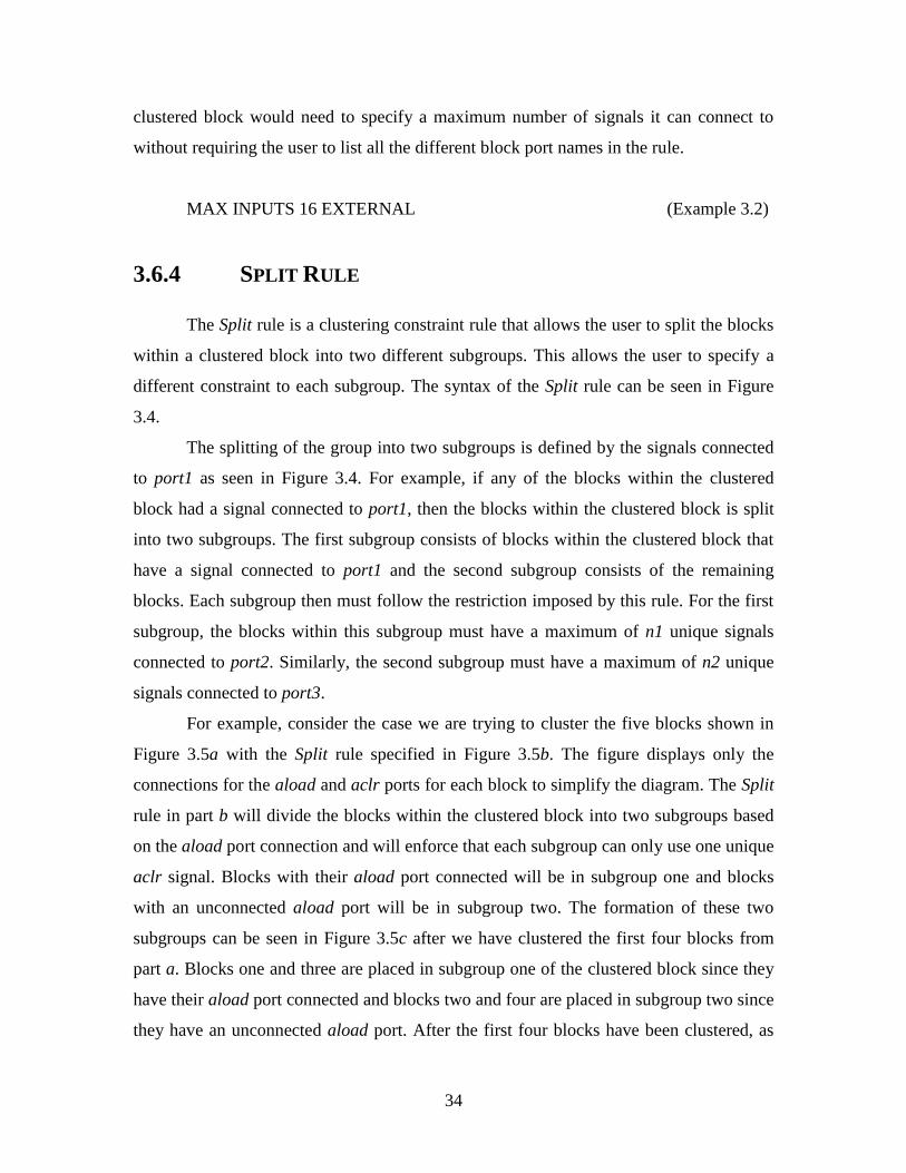
34
clustered block would need to specify a maximum number of signals it can connect to
without requiring the user to list all the different block port names in the rule.
MAX INPUTS 16 EXTERNAL (Example 3.2)
3.6.4 SPLIT RULE
The Split rule is a clustering constraint rule that allows the user to split the blocks
within a clustered block into two different subgroups. This allows the user to specify a
different constraint to each subgroup. The syntax of the Split rule can be seen in Figure
3.4.
The splitting of the group into two subgroups is defined by the signals connected
to port1 as seen in Figure 3.4. For example, if any of the blocks within the clustered
block had a signal connected to port1, then the blocks within the clustered block is split
into two subgroups. The first subgroup consists of blocks within the clustered block that
have a signal connected to port1 and the second subgroup consists of the remaining
blocks. Each subgroup then must follow the restriction imposed by this rule. For the first
subgroup, the blocks within this subgroup must have a maximum of n1 unique signals
connected to port2. Similarly, the second subgroup must have a maximum of n2 unique
signals connected to port3.
For example, consider the case we are trying to cluster the five blocks shown in
Figure 3.5a with the Split rule specified in Figure 3.5b. The figure displays only the
connections for the aload and aclr ports for each block to simplify the diagram. The Split
rule in part b will divide the blocks within the clustered block into two subgroups based
on the aload port connection and will enforce that each subgroup can only use one unique
aclr signal. Blocks with their aload port connected will be in subgroup one and blocks
with an unconnected aload port will be in subgroup two. The formation of these two
subgroups can be seen in Figure 3.5c after we have clustered the first four blocks from
part a. Blocks one and three are placed in subgroup one of the clustered block since they
have their aload port connected and blocks two and four are placed in subgroup two since
they have an unconnected aload port. After the first four blocks have been clustered, as

35
seen in part c, subgroup one uses only one aclr signal and subgroup two currently uses no
aclr signals. If we then try to add block 5 to this clustered block, the Split rule specified
in part b will disallow us from adding block 5 because it will make the current cluster
block illegal. Figure 3.5d illustrates the illegal clustered block that will be created if block
5 was added to the cluster; block 5 will be placed in subgroup one since it has a
connected aload port and it will increase the number of used aclr signals to two which is
one higher than what is permitted according to the Split rule in part b. Block 5 will have
to be placed in its own clustered block leaving the clustered block as seen in part c with
only 4 blocks.
3.6.5 PAIR RULE
The Pair rule is a clustering constraint rule that allows the user to identify signals
that are combined to generate internal signals within a cluster. The rule restricts that the
number of internal signals that can be generated from the two specified ports in each
clustered block to be at most n. This is useful because clustered blocks contain a limited
number of internal signals that are created from specific ports of a block. For example,
the clustered block may implement a specific internal signal generated from the
connections of two specific block ports to take advantage of a common property among
FPGA circuits, such as gated clocks. However the clustered block will have a restriction
on how many internal signals within a clustered block in order to satisfy the tradeoffs of
having extra logic within the clustered block and the size of the clustered block.
As illustrated in Figure 3.4, the Pair rule restricts the number of internal signals
that can be generated from the signals connected to port1 and port2 to a maximum of n.
For example, the Pair rule in example 3.3 limits the number of internal signals generated
from the clock and enable port connections to be no more than 2.
PAIR clock enable 2 EXTERNAL (Example 3.3)

36
Figure 3.5: An Example of how Subgroups are Created by the Split Rule
Blk 3
aload
aclr
Blk 4
aload
aclr
Blk 1
aload
aclr
Blk 2
aload
aclr
net1
net2
Subgroup 1
Subgroup 2
d) Illegal Cluster Created with Block 5 Added
Blk 5
aload
aclr net3
Illegal Cluster
2 unique
aclr signals
0 unique
aclr signals
Blk 3
aload
aclr
Blk 4
aload
aclr
Blk 1
aload
aclr
Blk 2
aload
aclr
net1
net2
Subgroup 1
Subgroup 2
c) Legal Cluster Created After First 4 Blocks are Added
Blk 5
aload
aclr
net1
net3
Legal Cluster
1 unique
aclr signal
0 unique
aclr signals
Blk 5
unclustered
Blk 3
aload
aclr
a) Five Blocks to Cluster
Blk 4
aload
aclr
Blk 1
aload
aclr
Blk 2
aload
aclr
net1
net2
b) Specified Split Rule
net1
Blk 5
aload
aclr
net1
net3
SPLIT aload aclr 1 aclr 1 INTERNAL

37
3.6.6 CONSTRAINT LANGUAGE EXAMPLE
The rules that make up the clustering constraint language implemented in the DC
tool are flexible enough to be able to model a wide range of FPGA architectures. An
example of the set of rules that can model a modern architecture is illustrated in
Figure 3.6. Parts a and b of the figure display the rules required to model the clustered
block of Altera’s Stratix and Cyclone FPGA family respectively.
Figure 3.6: Example of Clustering Constraint Rules
PAIR clk ena 2 INTERNAL
MAX aclr 2 INTERNAL
MAX aload 1 INTERNAL
SPLIT aload aclr 1 aclr 1 INTERNAL
MAX inverta 1 INTERNAL
PAIR sload sclr 1 INTERNAL
MAX clk ena aload sload aclr sclr inverta 6 EXTERNAL
IF sload ena 1 EXTERNAL
IF aload clk 1 EXTERNAL
MAX aclr sclr 2 EXTERNAL
MAX INPUTS 26 EXTERNAL
a) Clustering Constraint Rules for Altera’s Stratix Family
PAIR clk ena 2 INTERNAL
MAX aclr 2 INTERNAL
MAX aload 1 INTERNAL
SPLIT aload aclr 1 aclr 1 INTERNAL
MAX inverta 1 INTERNAL
PAIR sload sclr 1 INTERNAL
MAX clk ena aload sload aclr sclr inverta 6 EXTERNAL
IF sload ena 1 EXTERNAL
IF aload clk 1 EXTERNAL
MAX aclr sclr 2 EXTERNAL
MAX INPUTS 23 EXTERNAL
b) Clustering Constraint Rules for Altera’s Cyclone Family

38
The rules specified in Figure 3.6a and 3.6b are sufficient to completely specify the
clustered block architecture of Altera’s Stratix and Cyclone FPGA device family
respectively. The two architectures have similar use of the four rules, with the Stratix
FPGA containing a larger clustered block because it supports a larger number of inputs
into the clustered block. The use of the rules in Figure 3.6 demonstrates the ability of the
clustering constraint language to model real architectures used in the commercial industry
and the flexibility of the language.
3.7 CLUSTERING FPGA ARCHITECTURAL LANGUAGE
Having described the model used to represent an FPGA, we will now show the
language used to describe this model to the DC tool. The DC tool uses the Clustering
FPGA Architectural (CARCH) language to describe the FPGA architecture. The CARCH
language is a flexible tool that allows the user to model a wide range of FPGA
architectures. The language is used to describe the model of three basic elements of an
FPGA architecture: the sub-block information, the block information, and the clustered
block information. The importance of each element to describe an FPGA architecture is
discussed in Section 3.5. All FPGA architecture specific information that the DC tool
needs to perform clustering is specified using the CARCH language. The CARCH
language is imported into the DC tool through the CARCH file as illustrated in Figure
3.1. This section will provide a general outline of the important sections found in the
CARCH file. Refer to appendix A for the complete syntax on how to specify the
architecture of an FPGA in the CARCH file.
3.7.1 IDENTITY RULES
The CARCH language allows the user to provide identity information for each
element described in the CARCH file. The identity information is used by the DC tool to
match blocks in the netlist to block types described in the CARCH file. This is
accomplished through the use of identity rules that allow the user to specify how to match
a block in the netlist to a particular block type. There are three different types of identity
information that the user can specify: block type, port rules, and parameter rules. In most
cases, specifying the block type is all that is required to match blocks in the netlist to
block types in the CARCH file. However, a block type can have multiple

39
implementations and require further information to determine the type of block the
element represents. For example, a block type can consist of multiple sub-block types.
For the user to specify which sub-blocks a block type may consist of the user needs to
specify additional information using port rules and parameter rules.
Port rules compare the signal connected to the specified port to the value provided
by the user. A Parameter rule compares the value of the specified parameter to the value
provided by the user. There are four different port comparisons a user can specify in a
port rule: 1), check if the specified value Equals the value specified by the rule; 2), check
if the specified value is Not Equal to the value specified; 3), check if the specified port is
connected; and 4), check if the specified port is unconnected. The first two port
comparisons are also used for parameter comparison.
The identity rules provides the DC tool with the flexibility to model a wide range
of block types without any major changes to the clustering algorithms. For example, to
add a new circuit description that represents each block type in a different format, the
user simply needs to add a new parser for that language and update the identity rules of
each block type specified in the CARCH file to model the new set of blocks in the netlist.
3.7.2 UNCONNECTED PORT RULES
Unconnected ports of blocks can be connected to GND or VCC for certain
configurations of some block types. The clustering constraint language needs to be aware
of these connections to ensure the clustered block does not fail any of the clustering
constraint rules for the clustered block. The DC tool allows the user to specify the ports
that are connected to VCC or GND when unconnected for each block type configuration
in the CARCH file. The rules to specify the configuration for unconnected port rules
include: specifying the sub-block type of the block, and parameter rules. The parameter
rules are the same rules described in Section 3.7.1.
An unconnected port rule can be specified as seen in Figure 3.7. The rule in the
figure states that when port1 is unconnected and the block is in the specified
configuration, then assign the value, new_value, to port1. The user can specify the
configuration of the block using two types of conditions: 1), check if the block contains
the specified sub-block; and 2), compare the value of the given parameter to the

40
corresponding specified value for each parameter rule. The comparison that can be
performed for the parameter rules include checking if the values are equal or not equal,
as described in Section 3.7.1. An example of an unconnected port rule is seen in Figure
3.7b and specifies when the sload port is unconnected, it should be assigned the value of
GND when the specified block contains a flip flop sub-block type and the parameter of
synch_mode is set to on.
Figure 3.7: Unconnected Port Rule
Unconnected port rules are specified in the unconnected port rules section of a
block type definition in the CARCH file. The user is able to specify any number of
unconnected port rules for each block type in the architecture.
3.7.3 SUB-BLOCK INFORMATION
All of the sub-block information is specified in the define_sub_blocks section of
the CARCH file as seen in Appendix A. The user can specify all of the information for
each sub-block type including: port information, parameter information, and
identification information.
check_port <port1> <new_value = gnd | vcc>
sub_block_type EQ ff
num_param_rules < n>
rule <param1> <COND> < value1>
….
rule <paramn-1> <COND> < valuen-1>
end_check_port
a) Unconnected Port Rule:
check_port sload gnd
sub_block_type EQ ff # (optional)
num_param_rules 1
rule synch_mode EQ on
end_check_port
b) Example of the Unconnected Port Rule

41
Port information consists of specifying the number of inputs, outputs, and clock
ports of the sub-block. The user can select any combination of ports as long as each sub-
block contains at least one input port and one output port. Parameter information
describes the mode of the block type and is used to determine the configuration of the
block. The syntax for specifying the port and parameter information is seen in Appendix
A.
The identification information is a list of rules used by the parser when reading
the circuit netlist to determine which sub-blocks in the netlist match to which of the
specified sub-block types in the CARCH file. See Section 3.7.1 for more information on
the identification rules possible with the CARCH language. The identification rules
provided by the CARCH language allow the DC tool to be configurable and able to
model a wide variety of sub-block types that can be parsed in and used seamlessly with
the clustering algorithms.
3.7.4 BLOCK INFORMATION
Block information is specified in the define_blocks section of the CARCH file, as
seen in Appendix A. The user can specify sub-blocks, ports, parameters, and
identification information. Output ports are also specified as registered output or
combinational output; this is needed by the DC tool to perform timing analysis as
described in Section 3.4. The identification information is required to identify the type of
each block as the DC tool reads in the netlist.
The block information allows the user to specify how many sub-blocks the block
type may have if any. Block types that consist of sub-blocks are usually blocks that may
have vastly different sub components. One example of a complex block type is seen with
the stratix_lcell block type from Altera’s Stratix family. This block type may be
comprised of one flip flop, one LUT, or one flip flop and one LUT. This block type is
easily modeled with the use of the sub-block types LUT and flip flop.
3.7.5 CLUSTERED BLOCK INFORMATION
The clustered block information is specified in the define_clusters section of the
CARCH file as seen in Appendix A. Relevant details for each cluster block type include:
maximum number of blocks in each cluster, maximum number of unique inputs and

42
unique clock inputs it can route to the blocks within the clustered block, carry chain
information, identification information, cluster constraint rules, and maximum number of
possible clustered blocks in the modeled architecture.
The maximum number of inputs, unique clock inputs, and blocks are needed to
define limits to common architectural features seen in all clustered blocks. The
identification information is needed to determine which blocks can be clustered and is
achieved using identification rules that were described in Section 3.7.1. The maximum
number of clustered blocks is used by the clustering algorithm to inform the user if the
current clustering result will not fit on the modeled architecture.
The cluster constraint language is needed to specify the rules the clustering
algorithm must follow to ensure that each clustered block is legal. The clustering
constraint language is specified in Section 3.6 and provides information regarding each
cluster constraint rule. The cluster constraint language provides the DC tool with the
flexibility to model a wide range of FPGA architectures including Altera’s Stratix and
Cyclone families as illustrated in Figure 3.6.
The carry chain information in the CARCH file allows the user to identify which
blocks in the circuit are in carry chain formation. A block connected in a carry chain is
configured in a mode to perform addition faster than in normal mode. Figure 3.8 displays
the syntax to specify the carry chain information in the CARCH file. The user specifies
the input and output ports of the block that will be connected when the block is in carry
chain formation. For example, the carry chain information specified in Figure 3.8b
specifies cin as the input port and cout as the output port used to connect the carry chain.
The DC tool simply checks the connections of the specified ports to identify if the block
is in a carry chain formation. The block at the start of the carry chain formation is the
block with the carry chain input port unconnected and a connected carry chain output
port. The DC tool determines the next block in the carry chain by following the
connections along the carry chain output port of one block to the carry chain input port of
the next block.

43
Figure 3.8: Carry Chain Information
For the complete specification of an entire CARCH file see Appendix A. For an
example of a CARCH file for a real FPGA device see Appendix B which displays the
CARCH files required to model Altera’s Stratix and Cyclone devices.
3.8 CARRY CHAIN IMPLEMENTATION
The DC tool provides two methods to cluster carry chains: 1) treat blocks that are
in a carry chain as a special form of clustering; and 2) cluster blocks that are in carry
chains and blocks that are not in carry chain in the same clustering step.
Method one is possible since the DC tool provides the user with the ability to
perform multiple clustering attempts and cluster a different group of blocks in each
attempt. This is accomplished by specifying two cluster block types in the CARCH file.
The user can specify in one clustering attempt to identify only blocks that are part of
carry chains as possible blocks to cluster. This clustering attempt will result in only
blocks that are part of carry chains being grouped into clustered blocks; the remaining
blocks will remain ungrouped. In the second clustering attempt, the user can target the
remaining blocks to create the remaining clusters for the circuit. Method two is possible
since for each clustered block, the user is able to specify information that allows the DC
tool to recognize when the block is part of a carry chain as illustrated in Section 3.7.5.
The DC tool performs clustering by selecting a block to begin the start of a new
clustered block; the first block that is selected to start a clustered block is also referred to
as a seed block. The seed block that is chosen is believed to be the most critical
carry_chain <inport> <outport>
max_clusters_per_chain <n>
a) Carry Chain Information Syntax
carry_chain cin cout
max_clusters_per_chain 30
b) Example of Carry Chain Information

44
unclustered block in the circuit. The criticality of the block depends on the factors the
user wishes to optimize including timing factors and area factors. The next block that is
added to the clustered block is the block that is determined to have the most attraction to
the current cluster and does not make the current clustered block illegal according to the
cluster constraint rules specified by the user. The attraction of a block to the cluster also
depends on the factors the user wishes to optimize—common inputs and outputs the
selected block has with the blocks in the cluster, among other factors. The DC tool will
only allow a block in carry chain formation to be a seed block if the block is at the
beginning of the carry chain formation. Blocks that are identified to be in the middle or
end of a carry chain formation are clustered by the carry chain clustering process.
The DC tool performs carry chain clustering when it comes across a block that
has been identified as the start of a carry chain during the normal process of clustering.
Once the block that begins a carry chain is found, the next block that is added to the
cluster is the next block in the carry chain formation. The selection process for the next
block continues until the clustered block cannot add any more blocks or the entire carry
chain is clustered. If the carry chain has not been entirely clustered when the current
clustered block is full, then the seed for the next clustered block is the next block in the
carry chain. The chain of blocks that make up the carry chain could be clustered in
multiple clustered blocks. The DC tool keeps track of which clusters form each carry
chain and outputs this information along with the clustering information in the clustering
result file, CNET, which is read in by the Dynamic Placer (DP) tool as illustrated in
Figure 3.1. Knowledge of which blocks span a carry chain is needed by the DP tool
because it will allow the placement to be aware of the blocks that are part of a carry
chain; this will allow the DP tool to be able to move all the blocks in the carry chain
formation at once when finding the optimal placement. See Chapter 4 for more details
regarding the placement operation of the DP tool.
The benefit of having two methods to implement carry chain clustering is that it
allows the user to compare the benefits of being able to cluster carry chains with other
blocks in the circuit. This allows the start or end of a carry chain to be clustered with
other logical blocks in the circuit. Non carry chain blocks can only be clustered at the

45
start or end of a carry chain because once carry chain clustering commences the next
block chosen to be clustered must be the next block in the carry chain formation.
3.9 CHANGES MADE TO T-VPACK
The clustering algorithm used by the DC tool is based on the original algorithm
from T-VPack and is shown in Figure 3.9. The clustering algorithm creates clustered
blocks by greedily packing BLEs into a cluster, by choosing a seed BLE and then adding
the next BLE to the current cluster [2][3]. The algorithm is continued until the current
cluster is full or adding any remaining BLE would make the current clustered block
illegal as described in Section 2.2.1.
A number of changes were required to T-VPack to develop the DC tool in order to
model commercial FPGA architectures and implement the features of the DC tool. These
changes include adding a constraint checking engine to ensure the clusters created are
legal and the ability to cluster circuits with carry chains. Figure 3.9 displays the additions
made to T-VPack using pseudo code to show how the features of the DC tool are
implemented in the original code.
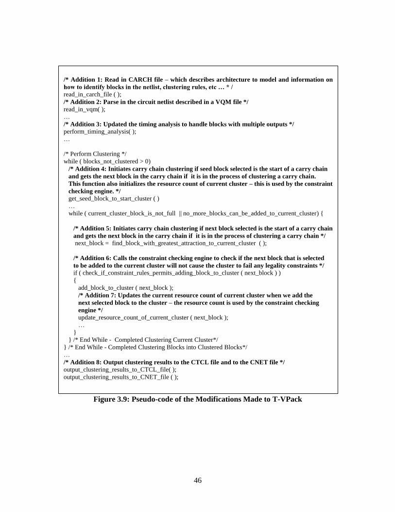
46
Figure 3.9: Pseudo-code of the Modifications Made to T-VPack
/* Addition 1: Read in CARCH file – which describes architecture to model and information on
how to identify blocks in the netlist, clustering rules, etc … * /
read_in_carch_file ( );
/* Addition 2: Parse in the circuit netlist described in a VQM file */
read_in_vqm( );
…
/* Addition 3: Updated the timing analysis to handle blocks with multiple outputs */
perform_timing_analysis( );
…
/* Perform Clustering */
while ( blocks_not_clustered > 0)
/* Addition 4: Initiates carry chain clustering if seed block selected is the start of a carry chain
and gets the next block in the carry chain if it is in the process of clustering a carry chain.
This function also initializes the resource count of current cluster – this is used by the constraint
checking engine. */
get_seed_block_to_start_cluster ( )
…
while ( current_cluster_block_is_not_full || no_more_blocks_can_be_added_to_current_cluster) {
/* Addition 5: Initiates carry chain clustering if next block selected is the start of a carry chain
and gets the next block in the carry chain if it is in the process of clustering a carry chain */
next_block = find_block_with_greatest_attraction_to_current_cluster ( );
/* Addition 6: Calls the constraint checking engine to check if the next block that is selected
to be added to the current cluster will not cause the cluster to fail any legality constraints */
if ( check_if_constraint_rules_permits_adding_block_to_cluster ( next_block ) )
{
add_block_to_cluster ( next_block );
/* Addition 7: Updates the current resource count of current cluster when we add the
next selected block to the cluster – the resource count is used by the constraint checking
engine */
update_resource_count_of_current_cluster ( next_block );
…
}
} /* End While - Completed Clustering Current Cluster*/
} /* End While - Completed Clustering Blocks into Clustered Blocks*/
…
/* Addition 8: Output clustering results to the CTCL file and to the CNET file */
output_clustering_results_to_CTCL_file( );
output_clustering_results_to_CNET_file ( );

47
3.10 CAPABILITIES OF THE DC TOOL
3.10.1 CLUSTERING CAPABILITY
The type of FPGA architectures that the DC tool can cluster is limited only by the
flexibility of the clustering constraint language. The DC tool is able to cluster any block
type that can be described in the CARCH file into a clustered block. The DC tool reads in
the circuit netlist and the architecture to model and outputs the clustering results as seen
in the CAD flow described by Figure 3.1.
The DC tool is able to perform multiple clustering iterations as defined by the
user through the CARCH file. The complete clustering information is then outputted in
two file formats; a clustering net (CNET) file and a clustering TCL (CTCL) script file.
The CNET file is used to import the clustering results into the DP tool. The CTCL file is
used to import the clustering results into Altera’s Quartus II CAD software tool. Being
able to import the clustering results into the Quartus II software allows comparisons of
the quality of the DC tool with that of the Quartus II commercial tool—these
comparisons are shown in Chapter 6.
The DC tool is capable of clustering a wide range of clustered block types due to
two main factors: the flexibility of the rules in the clustering constraint language, and the
wide range of block types the tool is able to model through the use of the CARCH
language. The ability to cluster a wide range of block types allows the DC tool to be used
to study the architectural design of a clustered block type. For example, the user can
determine whether fewer or more of a given port type is required. Determining the
number of connections a clustered block type should have for each port type will result in
the following area and speed benefits in the design of the architecture:
Removing redundant connections within a clustered block type will decrease the
size of the clustered block.
Adding useful connections will reduce the number of clusters that is required for a
given circuit but increase the size of a clustered block. Reducing the number of
clustered blocks to describe a circuit will improve Fmax of the circuit and decrease
the area the circuit consumes on the FPGA.

48
The ability to cluster blocks into carry chain formations furthers expands the
range of circuits that can be used for academic studies. The benefit of having two
methods to implement carry chain clustering allows the user to compare the benefits of
being able to cluster carry chains with other blocks in the circuit as is shown in Chapter 6.
The clustering implementation used by the DC tool allows the user to specify
multiple clustering attempts with the ability to specify multiple clustered blocks. Priority
is given to each clustered block by the order it is specified in the CARCH file. This
allows the user to experiment with selecting which group of blocks to cluster in each
attempt based on the block types, modes of the block, or common port connections.
3.10.2 CLUSTERING LIMITATION
The rules that currently make up the clustering constraint language have two
limitations: one, the cluster algorithm assumes that each block occupies only one position
within the clustered block; and two, the maximum number of block positions within a
clustered block is constant. These limitations restrict the DC tools ability to cluster more
complex block types such as memory blocks.
Memory block types are common in FPGA architectures and are found in devices
in a variety of sizes. The size of a memory block is defined by the number of address
locations the block can contain and the number of bits that can be accessed at each
location. The number of locations that can be addressed within a memory block is
referred as the memory block depth. The number of bits a memory block can access at
each address location is referred as the width of a memory block. Thus, the size of a
memory block is simply the number of bits it can store and is calculated by multiplying
the depth by the width. The memory block in the netlist may model a different depth and
width of the memory block and operate in a variety of modes. Architectures that contain
memory blocks will impose restrictions on how to cluster memory block elements into
clustered memory blocks.
The problem that arises with clustering memory blocks is similar to the
limitations that were discussed earlier on the clustering ability of the DC tool; first, the
memory blocks may occupy one or more positions within the clustered block depending
on the size of the memory block element; and secondly, the clustered memory block is no

49
longer constant size since there are different sized memory blocks on the device.
Complex blocks like memory blocks also bring up other challenges in the clustering
process such as ensuring the final clustering does not exceed any one type of clustered
memory block while ensuring the clustering is optimized. Similar problems exist for
other complex block types that are common in modern architectures.
The two limitations described in this section may also affect the architectures that
use complex logic blocks. Traditionally, FPGA architectures only used one K-input sized
LUT in the design of the BLE as seen in stratix_lcell design of Altera’s Stratix
architecture as described in Chapter 2. In recent architectures, the design of a BLE is no
longer restricted to one type of K-LUT. This is seen in Altera’s Stratix II and Stratix III
families which now support the implementation of LUTs of different sizes. The different
sized BLEs result in similar problems as discussed with memory blocks; the BLE may
now occupy more than one position within the clustered block. The current limitation
prevents the DC tool from being able to model the Altera’s Stratix II and III architectures.
The clustering constraint language can easily be extended to include the addition
of new rules. This provides the DC tool the ability to overcome the limitations discussed
in this section and can continually be extended in order to model the latest FPGA
architectures.
3.10.3 CLUSTERING FUTURE WORK
HIERARCHICAL CLUSTERING
The DC clustering capability can be extended to perform hierarchical clustering.
Hierarchical clustering is the process of clustering a clustered block. This is simply
allowing the user to specify a clustered block as the block type to cluster for the next
clustering iteration. Since the clustering flow already allows multiple clustering
iterations, the only change that is required to perform hierarchical clustering is to update
the circuit netlist with the results of the previous clustering attempt. Updating the netlist
with clustering results means adding the newly created clustered blocks to the list of
blocks in the netlist. The clustering algorithm and the clustering constraint language do
not require any further changes to achieve hierarchical clustering.
50
REGISTER PACKING
The first benefit of hierarchical clustering is to allow register packing to be
performed as one of the steps in clustering. Register packing pairs together LUTs and flip
flops into one block as was described in Chapter 2. The T-VPack tool previously only
performed simple register packing; it packed a flip flop with a LUT if the flip flop was
the only output of the LUT. The DC tool currently does not perform register packing.
Register packing can be viewed as a form of clustering since it simply groups together
two blocks to form one clustered block. The current clustering algorithm and constraint
rules can be used to perform register packing. The only additional work that may be
required is to add a two new clustering constraint rules: 1), a rule that will ensure the DC
tool will only pack flip flops and LUTs together that have some benefit and will leave
some flip flops and LUTs clustered by themselves; and 2), be able to cluster block types
together based on a direct connection between the two blocks as was done for carry chain
clustering.
ADDING NEW RULES
The clustering constraint language used by the DC tool is designed to be
extendible. New rules can be added to the clustering constraint language without any
changes required to the rules already present or the clustering algorithms. This makes the
DC tool extendible since the process of adding new rules is not intrusive. One example of
a rule that will expand the ability of the DC tool is a rule that allows the user to specify
the minimum gain that is required to add a block to the cluster. A minimum gain rule will
help the DC tool to perform register packing as described in the previous section and it
would allow the user to experiment with the clustering algorithm decisions. For example,
the minimum gain rule will ensure clustering only adds blocks to a cluster that have a
certain attraction to the clustered block. Adding the minimum gain rule will result in
clusters that do not have a maximum number of blocks and may help in the placement of
clustered blocks on the FPGA device. An experiment of this type is presented in Chapter
6.

51
CLUSTERING MORE COMPLEX BLOCK TYPES
Two other useful rules that can be added to the DC tool to expand its functionality
are: 1) allow the number of positions a block can occupy within a clustered block to be
variable, and 2) allow the maximum number of block positions of a clustered block to be
variable. These two rules will remove the limitations described in Section 3.10.2 and the
DC tool will be able to cluster complex block types such as memory blocks,
multiplication blocks, and architectures with multiple K-LUT sizes.
MODEL MORE COMPLEX ARCHITECTURES
The new rules described above would increase the range of architectures the DC
tool can model. These rules, combined with the ability to perform hierarchical clustering
would allow the DC tool to model Altera’s Stratix II and III architectures which require
three levels of hierarchical clustering as illustrated in Figure 3.10. The netlist produced
for these devices contains different sized LUTs and flip flops that are clustered together
to create the final clustered block. The DC tool can model the clustering required for a
Stratix II and III devices by using three levels of clustering. Level 1 requires clustering
the flip flop and LUT sub-blocks into blocks which is also referred to as register packing.
Level 2 clustering requires the DC tool to cluster these newly formed blocks into a
clustered block referred to as an ALM by Altera. An ALM cluster may contain up to 2
LUTs and 2 flip flops depending on the size of the LUTs. The third and final clustering
step requires clustering the newly formed ALMs into LAB blocks, as illustrated in Figure
3.10.
CLUSTERING ALGORITHM CHANGES
Currently the user can only change the clustering constraints of the clustering
algorithm. New rules can be added to allow the user to change how the clustering
algorithm selects the seed block or the next block to be added to the current cluster. This
would allow academic studies to investigate variations in the clustering algorithm.

52
Figure 3.10: Clustering Flow Required for Stratix II and Stratix III Architecture
F F L L L
F L F L L F L
F L
F L
L
F L
F L
F L
F
F L
L
F L
F L
F L
F L
F L
F L
F L
. . .
. . .
. . .
1. Parse in Netlist
2. Cluster LUTs and Flip Flops into Blocks
4. Cluster ALMs into LAB Blocks
F L F L . . .
3. Cluster Blocks into ALM Blocks
L F L
L F L F L F L
- LUT
- Flip Flop
L
F

53
4 DYNAMIC PLACER (DP)
4.1 DP OVERVIEW
The DP tool determines the placement of blocks for modern FPGA architectures.
Figure 4.1 demonstrates the CAD flow that is used with the DP tool. The CNET file is
generated by the DC tool and contains the clustering results of the circuit. The FPGA
architecture that is modeled by the DP tool is described using the Placement FPGA
Architecture (PARCH) language and is specified in the PARCH file. The DP tool reads in
the circuit information from the CNET file and the architecture information from the
PARCH file and performs the placement step in the FPGA CAD flow process as
described in Section 2.2.2. During placement, the DP tool interacts with the Placer Delay
Model (PLDM) interface to obtain inter-cell delay estimates as discussed in Section 4.4.1.
Figure 4.1: DP CAD Flow
Dynamic Placer (DP)
Quartus II (quartus_fit)
PTCL file
CNET file
PLDM Interface
PARCH file
Dynamic Clusterer (DC)

54
Currently the DP tool can only read in a CNET netlist produced by the DC tool. The
DC tool outputs the clustering results of the circuit in the CNET file as described in
Chapter 3. The CNET file is read in by the DP tool to perform the placement step in the
CAD flow as shown in Figure 4.1. The PTCL file is a TCL script file that is generated by
the DP tool to store the placement results via assignment statements that can be imported
into Altera’s Quartus II CAD software. Importing the placement results into Altera’s
Quartus II CAD software provides a way to measure the quality of the placement results
of the DP tool as described in Chapter 5.
DP is designed to be a dynamic tool because it can model a wide variety of FPGA
architectures. The flexibility of the DP tool was accomplished by modifying the code of
VPR to be configurable. Designing a configurable placement tool first requires
developing an interface language that is needed to describe various architectural features
of an FPGA device and algorithm features for FPGA CAD tools. VPR cannot model
modern FPGA architectures due to the limitations that were described in Section 2.2.2.
The placement algorithms used in VPR need to be modified to handle the configurable
design.
A configurable placement tool is able to model a wide range of FPGA architectures
without any modifications to the algorithms within the tool. A specific FPGA architecture
model will require algorithms within the placement tool to adapt to meet the needs of the
new FPGA design. For example, changing the positions where each block type is located
on an FPGA device will impact several algorithms within the placer. All the locations
where each block type is found on an FPGA is referred to as the floorplan. One algorithm
that is greatly affected by the floorplan of an FPGA is the placement algorithm. The
placer ensures that each block in the netlist will be placed in a legal position on the FPGA
device. Altering the floorplan of the FPGA architecture will directly impact the
placement algorithm since it needs to know the legal locations it can place each block on
the FPGA. The DP tool is able to model a wide range of architectures because its
configurable design allows the user to specify all the architecture information of an
FPGA, including the floorplan, and algorithm information from a file.

55
The changes that were made in VPR to create the DP tool are listed below:
Updated the placement and timing analysis algorithms to be configurable
Updated the timing analysis model
Update the parser to read in the CNET circuit description
Developed a new method to model the architecture of an FPGA
Created a placement FPGA architectural specification language
Added new functionality: the ability to model heterogeneous architectures and
place carry chains formations
The rest of this chapter will describe the implementation details and the capabilities of the
DP tool.
4.2 C ONFIGURABLE DESIGN
The DP tool was designed to be configurable by using general data structures to
store specific FPGA architectural and placement information. These data structures are
then accessed by the algorithms used in the DP tool to retrieve any FPGA architecture or
algorithm information. The algorithms within the DP tool were adapted to operate on any
type of FPGA architecture the tool is able to model. The flexibility of the configurable
design was achieved by implementing a dynamic Placement Architectural (PARCH)
description language which allows the user to specify a wide range of FPGA
architectures. The information specified with the PARCH language populates the general
data structures which are used by the algorithms of the DP tool.
The PARCH file is used to provide information regarding the FPGA architecture
model, and the timing analysis model required for the placement step in the FPGA CAD
flow. The versatility of the PARCH language is described in more detail in Section 4.6.
The flexibility of the timing analysis model that can be specified is further described in
Section 4.4.
4.3 FPGA ARCHITECTURE MODEL
The DP tool must be capable of modeling a wide range of architectures and
support the placement step in the FPGA CAD flow for the chosen architecture. The
model used to support clustering, as described in Chapter 3, possesses a different set of
requirements than the model required to support placement in the FPGA CAD flow as

56
seen in Figure 2.10. In Chapter 3, we explained in order for the DC tool to perform
clustering the tool must be able to model three elements: sub-blocks, blocks, and
clustered blocks. For placement, the DP tool only needs to be concerned with the
placement of blocks on the FPGA and only requires two elements to model the FPGA
architecture in order to perform placement: sub-blocks and blocks. The placement
algorithm tries to place the blocks in order to optimize either wire length, routability
across the FPGA, or maximize the circuit speed as discussed in Section 2.2.2. The FPGA
features that need to be modeled for the DP tool are shown in Figure 4.2. At the highest
level, we need to model elements that can be physically placed on the FPGA device such
as clustered blocks, RAM blocks, or similar resources; these are referred to as blocks in
the model. At the lowest level, we need to model elements that can be placed within a
block such as BLEs; such elements are referred to as sub-blocks in the model.
The BLE element was modeled as a block type for the DC tool, as explained in
Chapter 3, and is now modeled as a sub-block type for the DP tool due to the different
requirements needed by each individual architecture model. The placement algorithms
are only concerned with the placement of blocks on the FPGA and whether those blocks
contain sub-blocks. Blocks that contain sub-blocks and clustered blocks that are
composed of blocks are considered as the same element in the DP tool and are modeled
simply as blocks that are composed of sub-blocks.
4.3.1 SUB-BLOCK MODEL
Sub-blocks are elements that are used to create blocks. In the clustering step of the
FPGA CAD flow discussed in Chapter 3, the DC tool will group together these sub-
blocks to form blocks. For example, BLEs are sub-blocks for the placement architecture
because they are grouped together to create blocks. Sub-blocks are used to decompose a
block into smaller parts to make it easier to model in the PARCH file. The details of what
the user can specify for the sub-block is described in Section 4.6.1.

57
Figure 4.2: Example of an FPGA Architecture Model for Placement
Block A
Block B
Block C
Sub-block A
. . .
. . .
FPGA Architecture Model
Block
Sub-block (BLE)

58
Sub-blocks are required to model an FPGA architecture in order to perform
placement because it simplifies the timing model the user must specify for each block
type that is required for timing analysis as is described in Section 4.4. A timing model
describes the delays of all the possible connections within a block or sub-block type and
is required in order to perform timing driven placement. Timing models for complicated
blocks are more easily specified if the user is only required to specify the timing models
of all possible sub-blocks the block may contain. This avoids the need to specify every
permutation of sub-blocks configured within the block. Refer to Section 4.4 for more
information on the timing model used within the DP tool.
4.3.2 BLOCK MODEL
A block is an entity that can be physically placed on the FPGA device and is
usually constructed from sub-blocks. For example, in traditional FPGA architectures a
block can be composed of a number of sub-blocks, BLEs. Blocks that contain sub-blocks
are more complex, and each block can be composed of a different number of sub-blocks.
A block can also contain no sub-blocks as seen in many architectures. For
example, an I/O block can be modeled with out the use of sub-blocks. The timing models
of these blocks can be specified without the use of sub-blocks. The block information the
user can specify in the PARCH file is described in more detail in Section 4.6.2.
Block information is required to specify the architecture of an FPGA because
modern architectures now contain a selection of different block types as described in
Section 2.1.4. Allowing the user the ability to specify any number of block types for an
FPGA provides the DP tool with the flexibility to model a wide range of architectures.
4.4 TIMING ANALYSIS
A timing analysis model is required to determine an optimized placement of a
circuit on the FPGA to maximize the performance. The DP tool performs timing analysis
by creating a timing graph to model the delays in the circuit. The timing graph will need
to model all the delays in the circuit including the delays between inputs and outputs of
blocks and the internal delays within a block.
The timing graph used by the DP tool is simply a set of connected nodes that can
model the delays of the circuit. Any connected output port, connected input port, or

59
internal node within a block type is considered to be a node in the timing graph. Recall,
from Chapter 3, that the clustering timing analyzer only modeled each output as a
possible node in the timing graph. Modeling input nodes and internals nodes of blocks
allows the DP tool to model the internal delays within a block type more accurately.
Once the timing graph is created, the timing analysis algorithm used for
placement is the same one used for clustering. As discussed in Section 3.4, timing driven
placement works by identifying the longest paths in the timing graph and attempting to
place blocks in the circuit to minimize the delays of these paths. A path is a set of
connected nodes beginning at a source node and ending at a sink node. A source node is
usually one of the nodes created to represent a registered output of a block or an input pin
of the circuit. A sink node is usually one of the nodes created to represent a registered
output of a block or an output pin of the circuit.
The delays between blocks in the circuit are known as inter-cell delays. These
connection delays are dependent on the locations of the source block and the destination
block and need to be updated when either block is moved to a new location on the FPGA.
The delays between input and output ports within a given block are known as intra-cell
delays. These delays represent the internal connection delays of a block. The original
VPR is only able to model intra-cell delays for blocks consisting of a LUT and flip flop
as described in Chapter 2 while the DP tool is capable of modeling a more complex block
type by allowing the user to specify the timing block model. The timing graph used by
the DP tool is able to model a wide range of architectures because of its configurable
design.
The remainder of this section will describe in more detail how nodes are created
in the timing graph to model inter-cell and intra-cell delays.
4.4.1 INTER-CELL DELAYS
During placement, the DP tool uses the PLDM interface, provided by Altera, to
obtain inter-cell delay estimates, as seen in the DP flow shown in Figure 4.1. The PLDM
interface provides delays between two blocks on a given Altera device as a function of
the block’s location on the device. For Altera architectures, using the delay estimates
provided by the PLDM interface will provide a more fair comparison of the quality of the
60
DP tool to Altera’s commercial CAD tool, Quartus II, as described in Chapter 5. For
general architectures, the PLDM interface will provide inaccurate delays but still can be
used to model general architectures since the delays provided by the PLDM interface are
a function of the locations of the two blocks on the FPGA and still can be optimized by
the placement algorithms.
4.4.2 INTRA-CELL DELAYS
There are two types of intra-cell delays that need to be modeled by the DP tool.
The first type is the internal delays of sub-blocks and blocks without sub-blocks. These
connection delays simply represent the internal connections of these elements between
their inputs and output ports. The second type is the delays between blocks and their sub-
blocks. Both types of intra-cell delays are discussed in more detail in the following
sections.
INTRA-CELL DELAYS: DELAYS WITHIN A BLOCK OR SUB-
BLOCKS
The DP tool models intra-cell delays by providing the ability to specify the delays
of the internal connections of a block or sub-block. The user can specify a timing model
for each mode of the block or sub-block in the PARCH file as described in Section 4.6. A
timing model for a block consists of a set of connections between input, output, and
intermediate nodes. Input and output nodes represent the inputs and outputs of the block,
and intermediate nodes are internal nodes within the block. An intermediate and output
node can also be specified to be a register node which will allow the DP tool to properly
model internal registers and registered outputs of a block.
A register node has two additional delays associated with it, setup time delay and
clock-to-Q delay, which must be modeled in order to perform accurate timing analysis
calculations. Setup time delay is the amount of delay the signal must be stable at the input
of the register before the clock signal arrives at the register to capture the value of the
signal. Clock-to-Q delay is the amount of delay after the clock arrives at the register when
the value at the input of the register will have arrived at the output of the register. To
properly model both delays, the DP tool timing analysis translates a register node into

61
three intermediate nodes and an output node as illustrated in Figure 4.3. Part a of the
figure displays an example of a BLE the user may wish to model with a 2-input LUT and
a registered output. Part b of the figure demonstrates how this BLE is represented by the
timing graph before the registered node is translated into intermediate and output nodes.
Part c of the figure displays the final timing graph model that is used by the DP tool to
represent the BLE that includes the setup time and clock-to-Q delays in the timing graph.
As discussed in Section 4.4, nodes 6 and 7 seen in part c of the figure are the sink and
source nodes created for the register node.
Figure 4.3: How a Registered Node is Modeled by the DP Tool
2 - LUT Flip
Flop
a) BLE
Registered
Output LUT
Inputs
1
2
6 7 4
4
Input Node
Output Node
Intermediate Node
Registered Node
5
c) Final BLE Timing Model
LUT
Inputs
Registered
Output
Registered
Output 3
b) Intermediate BLE Timing Model
1
2
LUT
Inputs 3
Models
setup time
delay
Models
clock-to-Q
delay
Sink Node Source Node

62
Figure 4.4 displays a more complex example of the intra-cell connections for a
BLE block model. Part a of the figure displays an example of a BLE block model
consisting of a LUT and a flip flop. The flexibility of the DP tool’s intra-cell delay model
allows the user to specify connections from input nodes or intermediate nodes to output
nodes or intermediate nodes. Part b of the figure displays a corresponding intra-cell
timing model for the BLE.
INTRA-CELL DELAYS: DELAYS BETWEEN A BLOCK AND ITS
SUB-BLOCKS
The intra-cell delay models can only be specified for blocks without any sub-
blocks. For blocks that contain sub-blocks, the only delays that can be specified are the
delays between the block inputs/outputs and the sub-block inputs/outputs. Figure 4.5
displays the three possible connection delays between the block and its sub-blocks that
are modeled by the DP timing model. They include the delay from the block input port to
the sub-block input port, the delay from the sub-block output port to the block output
port, and the delay from the sub-block output port to any sub-block input port as seen in
the Figure 4.5. These connection delays can be specified for each block type in the
PARCH file.

63
Figure 4.4: Example of a Block Intra-Cell Timing Graph Model
1
LUT
a) BLE Model
Combinational
Output
Registered
Output
LUT
Inputs
Register
Inputs
2
3
4
7
5
9
Input Node
Output Node
Intermediate Node
8
b) BLE Timing Model
Register
Inputs
LUT
Inputs
Registered
Output
12
11
Combinational
Output
6
10
Flip
Flop

64
Figure 4.5: Block to Sub-block Connection Model
4.5 CLUSTERING NETLIST (CNET)
Currently, the DP tool can only read in the clustering netlist (CNET) description
language that is generated by the DC tool. The CNET file contains the clustering result of
the circuit that is produced by the DC tool. The original VPR tool read in a NET file
generated by T-VPack that could only describe circuits that contain one type of clustered
block, and input and output pins. The CNET circuit description language is a more full-
featured language that can describe more complex circuits and block types which support
the complete functionality of the DC and DP tools.
The CNET description language is able to model a more complex block type that
can provide information pertaining to the block type, the mode of the block, the
connections of the block, and any sub-block information. Each sub-block further provides
information about the sub-block block type, the mode of the sub-block, and the input and
output connections of the sub-block within the block.
Figure 4.6 displays an example of the syntax seen for a block in the netlist. Refer
to Appendix C for a complete example of a generated CNET file for a circuit. The order
of the input and output pins listed in the figure for the block or sub-block is specified by
Sub-block
1
Block
Sub-block
N
Sub-block Output Pin to
Sub-block Input Pin Delay
Sub-block Output Pin to
Block Output Pin Delay
Block Input Pin to
Sub-block Input Pin Delay

65
the PARCH file. An unconnected input or output port is specified as open in the CNET
file. The presence and the maximum number of sub-blocks within a block is also
specified by the PARCH file.
Figure 4.6: Syntax of a CNET file
The CNET file also contains information regarding carry chain formations. Refer
to Section 4.7 for more information on how the DP tool is able to place circuits with carry
chain formations. The carry chain information in the CNET file simply informs the DP
tool of each carry chain that spans at least two clustered blocks.
4.6 PLACEMENT FPGA ARCHITECTURE LANGUAGE
The DP tool uses the Placement FPGA Architectural (PARCH) language to
describe the FPGA architecture. The DP tool is able to model a wide variety of
architectures because of the flexibility of the PARCH language. The language is used to
describe the model of the two elements in an FPGA: sub-block information and block
information. The importance of each element to describe the architecture of an FPGA to
perform placement is described in Section 4.3.
The PARCH language provides the DP tool with the flexibility to specify the
floorplan of the FPGA, any number of block types, and any number of sub-block types.
This allows the DP tool model heterogeneous architectures. As described in Chapter 1,
heterogeneous FPGA architectures are more complex as they contain both an array of
programmable logic blocks and other types of specialized blocks. These specialized
blocks can perform specific functions such as multiplication or storage, are located at
clb <block_type> <block_name>
mode <block_mode>
pinlist: <pin_1> <pin_2> … <pin_n>
(in order as defined by clb inputs specified in .arch file)
subblock: <sub-block_type > <sub_block_mode> <sub_block_name> <pin_1> <pin_2> … <pin_n>
subblock: <sub-block_type > <sub_block_mode> <sub_block_name> <pin_1> <pin_2> … <pin_n>
subblock: <sub-block_type > <sub_block_mode> <sub_block_name> <pin_1> <pin_2> … <pin_n>
.
.
.

66
specific locations within the two-dimensional array of programmable logic blocks, and
could come in a variety of sizes on the FPGA device. Section 4.9 further discusses the
capabilities of the DP tool.
The PARCH language allows the user to provide all the necessary information
required by the DP tool to perform placement and is imported into the DP tool through
the PARCH file as illustrated in Figure 4.1. This section will provide a general outline of
the important sections found in the PARCH file. Refer to Appendix D for the complete
syntax on how to specify the architecture of an FPGA in the PARCH file.
4.6.1 SUB-BLOCK INFORMATION
Each sub-block is specified in the define_sub_block_type section of the PARCH
file as seen in Appendix D. The user can specify all the required information for each
sub-block type including: ports, timing model, and the identification of which
intermediate or output nodes are registered.
Port information consists of specifying the number of inputs, outputs, and clock
ports on the sub-block. The user is free to select any number of input ports and output
ports as long as each sub-block contains at least one input port and one output port. The
user is also able to specify any number of intermediate nodes to help describe the internal
connections of a sub-block as described in Section 4.4.
The timing model information specifies the delays between all possible internal
connections between any of the input ports, intermediate nodes, and output ports of a sub-
block type. The PARCH language provides the user with the ability to specify a timing
model for each mode of the sub-block, including any needed register delays, setup time
delay and clock-to-Q delays.
4.6.2 BLOCK INFORMATION
The user can specify information for each block type in the define_block_type
section of the PARCH file as seen in Appendix D. The user can specify all the required
information for each block type including: port information, timing model information,
identification of which nodes are registered, sub-block information, and floorplan
information.

67
Port information consists of specifying the number of inputs, outputs, clock ports
on the block. If the block type does not contain any sub-blocks, the user is also able to
specify any number of intermediate nodes to help describe the internal connections of a
block. Otherwise if the block type does contain sub-blocks, the user can specify the
maximum number of sub-blocks this block type can contain.
The timing model information specifies the delays between all possible internal
connections between any of the input ports, intermediate nodes, and output ports of a sub-
block type. If the block type does not contain any sub-blocks, the PARCH language
provides the ability to specify a timing model for each mode of the block. Otherwise, the
user can only specify the delays between input and output ports of the block and the input
and output ports of the sub-blocks. As similarly described for sub-blocks types, the user
is also able to specify which of the internal nodes or output ports are registered and their
associated register delays, setup time delay and clock-to-Q delay.
4.7 CARRY CHAIN IMPLEMENTATION
The DP tool has the ability to place circuits that contain carry chain formations. In
terms of placement, these elements are referred to as sub-blocks of the placement
architecture and can span multiple blocks. Chains that span multiple blocks require the
positions of these blocks to be placed adjacent to one another on the FPGA device in
order for the carry chain path to remain intact. For Altera devices, these blocks must be
placed vertical adjacent to one another as seen in Figure 4.7. Currently, the DP tool can
only support carry chains that need to be placed vertically adjacent to one another. As
discussed in Section 4.5, the carry chain information for the netlist is provided in the
CNET file. The placement algorithms in the DP tool are able to place circuits with carry
chains. The DP tool ensures the final placement of the circuit will have blocks in the
same carry chains placed vertically adjacent to one another and in the proper order.

68
Figure 4.7: Example of the Placement Required for a Carry Chain
4.8 CHANGES MADE TO VPR
The placement algorithm used by the DP tool is based on the original algorithm
from VPR and is shown in Figure 4.8. The placement algorithm uses a simulated
annealing placer which mimics the annealing process used to gradually cool molten metal
to produce high-quality metal objects [2][24]. The initial placement is created by
assigning clustered blocks randomly to the available locations in the FPGA. A large
The path the carry bit
information is rippled or
passed along in the
adder is outlined in red.
Blocks in carry chain
formation need to be
placed one after the
other to keep the carry
chain intact.
Attempting a move of
either one of these
blocks during placement
requires both blocks to
be moved keeping their
positions relative to each
other the same.
Portion of a Logic Block Array on an FPGA
. . .
.
.
.
Block
Sub-block

69
number of block moves are then made to gradually improve the placement as described in
Section 2.2.2.
A number of changes were required to VPR to develop the DP tool in order to
model commercial FPGA architectures and implement the features of the DP tool. These
changes include making the tool configurable and adding the ability to place carry chains.
Figure 4.8 displays the additions made to VPR using pseudo code to show how the
features of the DP tool are implemented in the original code.
4.9 CAPABILITIES OF THE DP TOOL
4.9.1 PLACEMENT CAPABILITY
Due to its configurable design the placement algorithm in the DP tool is able to
effectively perform the placement step on a wide range of architectures. The DP tool
builds up a list of valid locations a block can be moved to respecting any placement and
algorithm restrictions at the point in time the move is attempted. The placement algorithm
then simply evaluates the move and repeats this process until the cost function determines
the DP tool has achieved a suitable placement.
The placement algorithm is also capable of placing multiple blocks in one
location of the FPGA device. This is required since I/O clustering is more suitable to be
performed at this step in the flow and does not contain any constraints similar to logic
block clustering. This is possible as the user is able to specify the occupancy of each
block location on the FPGA device. The occupancy of a block location is usually one for
any other block type. I/O blocks usually have multiple instances located in the same
location on a FPGA device.

70
Figure 4.8: Pseudo-code of the Modifications Made to VPR
/* Addition 1: Read in PARCH file – which describes architecture to model and information on
how to identify blocks in the netlist, identify carry chains, etc … * /
read_in_parch_file ( );
/* Addition 2: Parse in the circuit netlist described in a CNET file */
read_in_CNET( );
…
/* Initial placement is created by randomly placing the blocks on the FPGA */
S = random_placement ( )
/* Set initial values for the simulated annealing algorithm */
T = initial_temperature ( )
Rlimit = initial_Rlimit ( )
While(exit_criterion ( ) == false) {
if ( check_need_to_perform_timing_analsyis( ) ){
/* Addition 3: Updated the timing analysis to handle configurable timing block models.
Timing analysis also interacts with PLDM interface to obtain timing delays between block
positions on the FPGA.
*/
perform_timing_analysis( );
}
…
/* Perform a number of moves at this temperature */
while( inner_loop_criterion () == false){
/* Generate a new placement by randomly selecting a block to move to a new location. */
/* Addition 4: If the block selected to move is part of a carry chain that span multiple
blocks, it will move all the blocks in the carry chain in the same move. */
Snew = generate_new_placement_by_moving_a_block (S, Rlimit)
/* Determine if the new placement should be accepted */
if (check_if_should_accept_new_placement ( Snew ) ){
S = Snew
}
if ( check_if_need_to_perform_timing_analsyis( ) ){
/* Addition 3: Described above */
perform_timing_analysis( );
}
}
/* Update the values of the simulated annealing algorithm – Lower the temperature */
T = update_temp()
Rlimit = update_Rlimit();
}
…
/* Addition 5: Output placement results to the PTCL file */
output_placement_results_to_PTCL_file( );
71
4.9.2 PLACEMENT LIMITATION
Currently the DP tool assumes all clocks in the circuit arrive at their destination at
the same time which assumes the circuit is not affected by clock skew. Clock skew is the
effect of the delays associated with routing the clock to the registers in the circuit on the
FPGA. This can result with registers having different clock delays and implies that
registers with the same clock in the circuit will have a different clock arrival time. The
DP tool currently assumes that the circuit can only contain one clock and performs timing
analysis base on this assumption on circuits with multiple clocks. In order for the DP tool
to place circuits with multiple clocks more effectively the timing analysis needs to be
updated to handle multiple clocks and the effects of clock skew on the delays in the
circuit.
4.9.3 PLACEMENT FUTURE WORK
This section suggests the following two candidates for future extensions of the DP
tool:
Region Moves
Sub-block Moves
SUPPORT REGION MOVES
Currently the DP tool is capable of moving multiple blocks at one time for carry
chain formations. This ability can be extended to apply to any group of blocks in any
sized region. This will allow the DC tool or user to attempt to predict which blocks
should be place near each other on the FPGA device. The positions of the blocks within
the region can also be set to be non-fixed unlike carry chains which require each block in
the region to remain in the same relative location with respect to each other.
Region moves are supported in modern commercial FPGA CAD tools as seen
with Altera’s commercial CAD tool, Quartus II, which refer to regions as LogicLock
Regions. Supporting region moves would allow academic researchers to investigate
clustering algorithms that can attempt to determine which clustered blocks should be
placed near each other; this can be viewed as another form of hierarchical clustering.
72
SUPPORT SUB-BLOCK MOVES
The DP tool is only capable of analyzing move attempts of blocks in the circuit.
The DP tool can be expanded to attempt moves of the sub-blocks within different blocks.
To attempt sub-block moves, the DP tool needs to be able to check the constraints of the
clustered blocks in order to ensure they are able to move the selected sub-block into the
selected block; this requires the DP tool to have a clustering constraint checker similar to
the one used by the DC tool. The DP tool will be required to implement the clustering
constraint language used by the DC tool in order to be able to check the same constraints.
Adding sub-block moves will expand the academic studies that can be performed on the
placement algorithm.

73
5 EXPERIMENTAL METHODOLOGIES
5.1 INTRODUCTION
This chapter will describe the procedures followed to obtain a set of results which
will be presented in Chapter 6. In particular, this chapter will discuss in detail how the
experiments were run, the circuits included in the benchmark set, the settings used in
each tool, the experimental test flow, and the data collected to analyze the results.
5.2 FPGA ARCHITECTURE MODEL
The results obtained in this thesis use two architectural models to illustrate the
ability of the DC and DP tools. The two architecture families that were modeled are
Altera’s Stratix and Cyclone devices. The specifications of the device used from both
families can be seen in Table 5.1. Running the circuits on a device from both families
will illustrate the flexibility of the DC and DP tools and it will further validate the results
produced by the tools.
Family Device Num of
I/O
Blocks
Num of
BLE Blocks
Num of
Memory
Blocks
Num of
Multiplication
Blocks
Stratix EP1S10F484C5 426 10 570 155 6
Cyclone EP1C3T144C6 104 2 910 13 0
Table 5.1: Specifications of the FPGA Architecture Modeled
The Stratix device used is a larger FPGA architecture compared to the Cyclone
architecture and is designed to achieve a greater performance. The Cyclone device can
only fit a subset of the circuits in the benchmark set due to the limited number of
available I/O and BLE blocks on the device that are required by the some of the circuits
in the benchmark set.
74
The complete specification of the Stratix and Cyclone architecture used in the
experiments is described by the clustering and placement architecture files, CARCH and
PARCH files. The Stratix and Cyclone CARCH and PARCH files used in the
experiments can be found in Appendix B and E.
5.3 BENCHMARK SET
The benchmark set used in the experiments was provided by [15] and consist of
27 different circuits as shown in Table 5.2. The circuits in the benchmark set contain only
two block types, I/O blocks and BLEs. As seen in the table, the benchmark set consists of
circuits from a variety of areas including encryption type circuits, control logic type
circuits, and audio/video circuits. The circuits in the benchmark set vary in size from a
small number of BLEs to over 5000 BLEs. There are also 13 circuits that make use of
carry chain logic as seen in Table 5.2.
The architecture modeled by the DC and DP tools does have other block types
besides I/O and BLE block types which are not currently supported by the DC tool such
as memory blocks and multiplication blocks. The DC tool clustering capability currently
cannot cluster these specific block types on the FPGA device. Thus, we are limited to use
circuits that only contain I/O and BLE block types. However, we are able to use
architectures with unsupported block types because the DP tool models the locations of
these block types as keep-out regions to ensure BLEs are not placed in these invalid
locations on the FPGA. The list of valid locations where BLEs can be placed in an FPGA
is specified in the PARCH file.
5.4 SEED SWEEPING
Each result in all the experiments performed was obtained by averaging the
results from three different placement attempts of the circuit. This was accomplished by
giving the placement function a different seed number which is used by the CAD tool to
control the initial state of random functions. For example, each different seed number
used by the placement tool will generate a different random initial placement of the
blocks on the FPGA device. Averaging the results of the three attempts for each circuit
prevents the results from being affected by an unlucky or lucky initial seed chosen by the
placer. The process of running the same circuit with different seed numbers is referred to

75
as seed sweeping. The benefit of seed sweeping is it allows a more fair evaluation when
comparing the quality of different CAD tools or analyzing the performance change due to
an algorithm improvement.
Benchmark
Name
Num
of IO
blocks
Num of
BLE
blocks
Uses
Carry
Chains
Fits In
Stratix
Device
Fits in
Cyclone
Device
Description
barrel16 38 129 No Yes Yes Simple HDL
barrel16a 26 107 No Yes Yes Simple HDL
barrel32 71 322 No Yes Yes Simple HDL
barrel64 136 882 No Yes No Simple HDL
fip_cordic_cla 53 412 No Yes Yes IP Core
mux32_16bit 54 853 No Yes Yes Simple HDL
mux64_16bit 87 1702 No Yes Yes Simple HDL
mux8_128bit 140 1667 No Yes No Simple HDL
mux8_64bit 76 835 No Yes Yes Simple HDL
oc_des_area_opt 189 691 No Yes No Encryption
oc_des_des3area 304 1135 No Yes No Encryption
oc_des_perf_opt 185 5336 No Yes No Encryption
ts_mike_fsm 15 16 No Yes Yes Finite State
Machine
xbar_16x16 97 176 No Yes Yes 1-bit 16x16
fip_cordic_rca 53 425 Yes Yes Yes IP Core
nut_000 314 631 Yes Yes No Auto Generated
nut_002 122 500 Yes Yes No Auto Generated
nut_004 321 337 Yes Yes No Auto Generated
oc_ata_ocidec1 125 540 Yes Yes No Control Logic
oc_ata_ocidec2 125 588 Yes Yes No Control Logic
oc_ata_v 125 290 Yes Yes No Control Logic
oc_cordic_p2r 82 1016 Yes Yes Yes Audio/Video
oc_cordic_r2p 74 1426 Yes Yes Yes Audio/Video
oc_correlator 85 478 Yes Yes Yes Audio/Video
oc_i2c 33 293 Yes Yes Yes Control Logic
oc_video_
compression_
systems_
huffman_dec
23 649 Yes Yes Yes Audio/Video
oc_video_
compression_
systems_
huffman_enc
23 613 Yes Yes Yes Audio/Video
Table 5.2: Properties of Circuits in Benchmark Set

76
5.5 TEST FLOW
The results obtained in this thesis were obtained using three different test flows:
the Quartus II test flow, the DC test flow, and the DP test flow as illustrated in Figure 5.1.
Three test flows are required in order to compare the quality of the results from the DC
tool and the DP tool to a commercial CAD tool, Quartus II. The details and the need for
each test flow are further described in the following sections.
5.5.1 THE QUARTUS II TEST FLOW
The Quartus II Test flow is required to obtain a set of results produced by a
commercial CAD tool, Quartus II. These results can then be used to compare and
measure the quality of the results produced by the DC and DP tools. The Quartus II test
flow requires running the benchmark set using only Quartus II CAD tools which consist
of quartus_map, quartus_fit, and quartus_tan. As seen Figure 5.1, in this flow
quartus_map performs the synthesis and technology mapping step of the CAD flow and
quartus_fit performs the clustering, placement, and routing steps of the CAD flow. The
final step, timing analysis, is perform by quartus_tan and is used to measure the
performance achieved. This flow provides the results of the Quartus II CAD tool, which
is then used as a comparison for the quality of the DC and DP tools.
5.5.2 THE DC TEST FLOW
The DC test flow is required to obtain the clustering results produced by the DC
tool as seen in Figure 5.1. In this flow, quartus_map performs the synthesis and
technology mapping step of the CAD flow. The DC tool then performs the clustering step
and the clustering results are imported into the quartus_fit module, which then performs
the placement and routing step. The final step, timing analysis, is perform by quartus_tan
and is used to measure the performance achieved. This flow allows a comparison of the
clustering of the DC tool to the clustering produced by Quartus II.

77
Figure 5.1: Experimental Test Flow
5.5.3 THE DP TEST FLOW
The DP test flow is required to obtain the placement results produced by the DP
tool as seen in Figure 5.1. In this flow, quartus_map performs the synthesis and
Circuit
Quartus II
(quartus_map)
Quartus II
(quartus_fit)
VQM
TCL
Results
DC Test Flow: Quartus II Test Flow:
Quartus II
(quartus_tan)
Circuit
Quartus II
(quartus_map)
Quartus II
(quartus_fit)
VQM
TCL
Results
DP Test Flow:
Quartus II
(quartus_tan)
CNET
Quartus II
(quartus_fit)
Results
Quartus II
(quartus_tan)
Circuit
Quartus II
(quartus_map)
Synthesis &
Technology
Mapping
Clustering
Placement
Routing
Timing
Analysis
DC
DC
DP
78
technology mapping step of the CAD flow. The DC tool performs the clustering step, and
then the DP tool performs placement. The placement produced is then imported into
quartus_fit, which performs the routing step. Finally, timing analysis is performed by
quartus_tan. This flow can measure the quality of the placement produced by the DP tool
by comparing the results from this flow to the results of the DC test flow. In both flows,
the DC tool produces the clustering results leaving the placement tool used as the only
difference between the two flows. The DP test flow can also be compared to the Quartus
II test flow to measure both the clustering and placement results produced by the DC and
DP tool compared to quartus_fit.
5.6 TOOL SETTINGS
To ensure a fair comparison was made between the tools created, DC and DP, and
the tools used to measure against, Quartus II, various tool settings must be made to ensure
a fair comparison. For each experiment, all tools were set to generate a result that focused
on improving the timing of the circuit. Thus, the goal of each CAD tool was to generate a
result that achieved the highest speed the clock could operate in the circuit which has
been referred to as the Fmax of the circuit. The complete list of all the settings used to
provide a fair comparison between the tools can be seen in Appendix F.
5.7 METRICS
To measure and compare the quality of the results three metrics were analyzed:
the maximum frequency, Fmax, that could be achieved by the circuit, the amount of wire
used in the circuit, and the runtime required to perform the clustering and placement steps
of the FPGA CAD flow. The remainder of this section describes the importance of each
metric.
5.7.1 MAXIMUM FREQUENCY (FMAX)
The Fmax achieved by a circuit is the most important of the three metrics to
analyze since each tool was programmed to optimize for this particular metric. This
metric, once again, refers to the speed at which the clock in a circuit can achieve while
still maintaining the functionality of the original circuit. The tool that obtains the higher
Fmax for a set of circuits is considered to have achieved the better result. This result is

79
obtained by running the timing analyzer, quartus_tan, to analyze the implementation of
each circuit and determine the Fmax achieved.
5.7.2 WIRE
Wire is the amount of routing resources required to connect each of the logic
block inputs and outputs in the circuit. This metric is important as it determines how
efficiently each logic block is placed within the FPGA. Specifically, this metric will
assess how effectively the tool grouped and placed non critical blocks on the FPGA. The
better placement of all blocks in the FPGA will result in a lower wire usage; thus, the
lower wire usage achieved is considered the better the result when analyzing this metric.
This metric was calculated by summing up the number of horizontal and vertical
channels consumed by the circuit. We ignore connections within a clustered block and
only consider connections outside the clustered blocks. This result is obtained by the
Quartus II routing tool, quartus_fit, which provides the amount of routing resources used
after routing the circuit.
5.7.3 RUNTIME
Runtime is the amount of time the tools consumed to perform the required
operation, the clustering and placement steps of the CAD flow. To ensure this metric is
consistent, all experiments were run on the same computer.
This metric was calculated by measuring the amount of time each operation,
clustering and placement, took to complete. This metric is important as it measures the
efficiency of the algorithms used to perform all the required operations. The least amount
of runtime needed to complete an operation is considered the better result when analyzing
this metric.

80
6 RESULTS
6.1 INTRODUCTION
The DC and DP tools are designed to meet two goals: 1) perform the clustering
and placement step in the FPGA CAD flow for complex architectures, including modern
FPGA architectures; and 2) achieve a performance quality comparable to commercial
FPGA CAD tools.
This chapter will demonstrate the successful completion of these two goals by
first illustrating the flexibility of the DC and DP tools by clustering and placing several
benchmark circuits on two different types of commercial architectures, Altera’s Stratix
and Cyclone FPGA family. Secondly, the quality of the clustering and placement
produced by the DC and DP tools is demonstrated by comparing the results achieved by
the DC and DP tools to the results produced by a commercial CAD tool, Altera’s Quartus
II CAD software.
At the end of this chapter we describe experiments that we have performed to
investigate different aspects of FPGA CAD tool design that demonstrates a small sample
of how the DC and DP tools can be used to pursue FPGA research by the academic
community.
6.2 DC AND DP RESULTS
6.2.1 RESULT QUALITY OF DC VERSUS QUARTUS II
The clustering quality of the DC tool was obtained by comparing the DC test flow
to the Quartus II test flow. Comparing these two flows evaluates the clustering results of
the DC tool to the clustering results produced by Quartus II, as described in Section 5.5.
The clustering results produced by the DC tool obtained from the DC test flow are shown

81
in Table 6.1 which lists the Fmax, the amount of wire required, and the runtime achieved
for each circuit in the benchmark set.
Circuit
Fmax (MHz) Wire Runtime
(seconds)
Stratix Cyclone Stratix Cyclone Stratix Cyclone
barrel16 220.4 217.1 1057.3 941.3 1 2
barrel16a 213.9 213.8 1266.7 1122.7 2 2
barrel32 155.4 158.0 3045.3 2754.7 2 3
barrel64 126.3 -- 12605.3 -- 11 --
fip_cordic_cla 62.7 61.7 5021.3 3897.3 3 3
mux32_16bit 226.3 225.5 6346.7 4713.3 7 6
mux64_16bit 175.5 171.6 18380.0 13364.0 19 16
mux8_128bit 287.1 -- 10792.0 -- 8 --
mux8_64bit 311.0 311.3 4326.7 4116.0 4 4
oc_des_area_opt 169.1 -- 10325.3 -- 6 --
oc_des_des3area 167.8 -- 20426.7 -- 22 --
oc_des_perf_opt 145.6 -- 69110.7 -- 17 --
ts_mike_fsm 422.1 405.2 141.3 92.0 0 1
xbar_16x16 307.4 310.0 3068.0 2518.7 3 3
fip_cordic_rca 82.4 81.4 5098.7 3078.7 1 3
nut_000 47.0 -- 5413.3 -- 7 --
nut_002 112.6 -- 4433.3 -- 5 --
nut_004 146.0 -- 2442.7 -- 4 --
oc_ata_ocidec1 248.5 -- 5212.0 -- 6 --
oc_ata_ocidec2 213.5 -- 6728.0 -- 9 --
oc_ata_v 239.0 -- 3936.0 -- 2 --
oc_cordic_p2r 231.3 222.3 9652.0 7736.0 7 5
oc_cordic_r2p 220.8 212.0 13200.0 10505.3 8 6
oc_correlator 21.2 19.9 2992.0 2240.0 2 3
oc_i2c 194.3 191.6 2868.0 2034.7 7 4
oc_video_compression_
systems_huffman_dec 118.5 114.8 7910.7 5861.3 12 9
oc_video_compression_
systems_huffman_enc 209.1 200.4 4350.7 3052.0 4 5
Table 6.1: Results from the DC Test Flow
The quality of the DC tool is indicated by the results shown in Table 6.2, which
compares the results of the DC tool to Quartus II, on the benchmark set. The table
demonstrates the DC tool achieves an average Fmax of 92.1% on the Stratix FPGA and
96.9% on the Cyclone FPGA compared to the Fmax achieved by Quartus II. The Fmax

82
achieved by the DC tool produces a small increase in the amount of wire used as the
clustering results of the DC tool requires on average an 8.1% and 4.9% additional wire to
route the circuits on the Stratix and Cyclone FPGA respectively as seen in the table. The
runtime of the DC tool is fast as it only takes on average 6.6 seconds and 4.7 seconds to
run for the Stratix and Cyclone FPGA respectively. The run time of the clustering
operation for Quartus II is not available and prevents us from comparing the runtimes of
the clustering tools.
Circuit Fmax Wire
Stratix Cyclone Stratix Cyclone
barrel16 99.1% 101.8% 73.5% 83.0%
barrel16a 95.7% 97.0% 66.0% 92.2%
barrel32 94.5% 95.3% 73.0% 93.3%
barrel64 92.0% -- 99.0% --
fip_cordic_cla 93.6% 98.8% 92.6% 100.8%
mux32_16bit 98.6% 98.0% 98.6% 114.2%
mux64_16bit 91.8% 92.8% 124.1% 119.8%
mux8_128bit 100.9% -- 103.4% --
mux8_64bit 98.1% 96.2% 80.7% 101.1%
oc_des_area_opt 83.0% -- 92.5% --
oc_des_des3area 83.4% -- 108.4% --
oc_des_perf_opt 73.7% -- 146.7% --
ts_mike_fsm 100.0% 100.0% 176.7% 119.0%
xbar_16x16 97.0% 102.7% 80.9% 105.3%
fip_cordic_rca 85.6% 88.3% 106.8% 89.2%
nut_000 81.7% -- 155.9% --
nut_002 85.8% -- 143.9% --
nut_004 83.8% -- 117.1% --
oc_ata_ocidec1 93.4% -- 90.1% --
oc_ata_ocidec2 83.3% -- 108.8% --
oc_ata_v 96.7% -- 87.8% --
oc_cordic_p2r 96.5% 96.2% 112.2% 105.4%
oc_cordic_r2p 95.5% 94.7% 118.5% 112.3%
oc_correlator 92.8% 95.6% 96.7% 121.5%
oc_i2c 94.1% 97.6% 129.0% 113.5%
oc_video_compression_
systems_huffman_dec 98.1% 96.5% 108.6% 102.4%
oc_video_compression_
systems_huffman_enc 97.4% 98.1% 127.7% 106.2%
Average 92.1% 96.9% 108.1% 104.9%
Table 6.2: DC Clustering Quality Compared to Quartus II

83
The results achieved demonstrate the DC tool is able to target different types of
commercial FPGA families and produce a result that is within 9% of a commercial tool,
which indicates a good quality of result.
6.2.2 RESULT QUALITY OF DP VERSUS QUARTUS II
The placement quality of the DP tool was obtained by comparing the DP test flow
to the DC test flow. In both of these flows, the clustering produced is from the DC tool.
Comparing these two flows will assess the placement quality of the DP tool to the
placement produced by the commercial CAD tool, Quartus II, as described in Section 5.5.
The DP test flow results are shown in Table 6.3 which lists the Fmax, the amount of wire
required, and the runtime achieved for each circuit in the benchmark set.
The placement quality achieved is summarized in Table 6.4, which compares the
DP tools’ results to Quartus II’s results. The table demonstrates the placement produced
by DP tool achieves an average Fmax of 98.3% on the Stratix FPGA and 96.1% on the
Cyclone FPGA when compared to the placement produced by the commercial CAD tool,
Quartus II. The Fmax achieved by the DP tool produces a decrease in wire use as the
placement results of the DP tool requires on average 5.3% and 13.0% less wire to route
the circuit on the Stratix and Cyclone FPGA respectively as seen in the table. The
runtime required to run the DP tool is significant higher compared to the Quartus II CAD
tool as the DP tool takes on average 19 times and 12 times longer to run on Stratix FPGA
and Cyclone FPGA respectively when compared to the Quartus II runtimes.
The results achieved demonstrate the flexibility of the DP tool to target different
FPGA families while achieving an Fmax within 4%, and a decrease in wire use, when
compared to a commercial tool.
6.2.3 RESULT QUALITY OF DC AND DP TOOLS VERSUS
QUARTUS II
This section summarizes the clustering and placement results that were obtained
using the DC and DP tools in the CAD flow described in the previous sections. The
quality of the DC and DP tools were analyzed by comparing the DP test flow to the
Quartus II test flow. Comparing these two flows evaluates the clustering and placement

84
results of the DC and DP tools compared to the clustering and placement results produced
by the commercial CAD tool, Quartus II, as described in Section 5.5. The clustering and
placement results of the DC and DP tools from the DP test flow are shown in Table 6.3.
Circuit Fmax Wire Runtime (seconds)
Stratix Cyclone Stratix Cyclone Stratix Cyclone
barrel16 223.2 213.1 1289.3 884.0 8 5
barrel16a 214.2 207.2 1529.3 1061.3 9 6
barrel32 166.2 154.2 3328.0 2270.7 25 16
barrel64 128.5 -- 10848.0 -- 78 --
fip_cordic_cla 61.2 57.1 4366.7 3201.3 22 17
mux32_16bit 221.7 212.8 5397.3 3874.7 37 24
mux64_16bit 180.9 169.5 15896.0 11297.3 97 61
mux8_128bit 293.8 -- 9088.0 -- 113 --
mux8_64bit 300.5 300.5 4241.3 3078.7 42 28
oc_des_area_opt 162.8 -- 10870.7 -- 91 --
oc_des_des3area 180.0 -- 19993.3 -- 187 --
oc_des_perf_opt 148.7 -- 59064.0 -- 441 --
ts_mike_fsm 422.1 405.2 89.3 94.7 1 1
xbar_16x16 311.0 312.6 3597.3 2398.7 24 14
fip_cordic_rca 83.4 77.9 4162.7 2833.3 35 19
nut_000 47.4 -- 3656.0 -- 210 --
nut_002 110.9 -- 3500.0 -- 58 --
nut_004 140.4 -- 2613.3 -- 166 --
oc_ata_ocidec1 206.8 -- 6189.3 -- 53 --
oc_ata_ocidec2 198.5 -- 7286.7 -- 65 --
oc_ata_v 198.7 -- 4680.0 -- 41 --
oc_cordic_p2r 221.4 199.1 7866.7 5642.7 449 249
oc_cordic_r2p 200.2 189.0 11373.3 9149.3 705 412
oc_correlator 23.7 21.3 3174.7 1818.7 35 22
oc_i2c 185.5 173.9 2449.3 1818.7 14 11
oc_video_compression_
systems_huffman_dec 115.3 108.4 6529.3 5137.3 24 18
oc_video_compression_
systems_huffman_enc 195.7 192.5 3781.3 2702.7 22 15
Table 6.3: Results from the DP Test Flow

85
Circuit Fmax Wire Runtime
Stratix Cyclone Stratix Cyclone Stratix Cyclone
barrel16 101.2% 98.2% 121.9% 93.9% 100.0% 100.0%
barrel16a 100.2% 96.9% 120.7% 94.5% 866.7% 100.0%
barrel32 107.0% 97.6% 109.3% 82.4% 1250.0% 1566.7%
barrel64 101.7% -- 86.1% -- 975.0% --
fip_cordic_cla 97.7% 92.6% 87.0% 82.1% 744.4% 833.3%
mux32_16bit 98.0% 94.4% 85.0% 82.2% 740.0% 800.0%
mux64_16bit 103.1% 98.8% 86.5% 84.5% 808.3% 796.5%
mux8_128bit 102.3% -- 84.2% -- 804.8% --
mux8_64bit 96.6% 96.5% 98.0% 74.8% 846.7% 922.2%
oc_des_area_opt 96.3% -- 105.3% -- 1820.0% --
oc_des_des3area 107.3% -- 97.9% -- 2666.7% --
oc_des_perf_opt 102.1% -- 85.5% -- 1160.5% --
ts_mike_fsm 100.0% 100.0% 63.2% 102.9% 100.0% 100.0%
xbar_16x16 101.2% 100.8% 117.3% 95.2% 100.0% 100.0%
fip_cordic_rca 101.1% 95.7% 81.6% 92.0% 883.3% 933.3%
nut_000 100.8% -- 67.5% -- 7011.1% --
nut_002 98.5% -- 78.9% -- 2900.0% --
nut_004 96.2% -- 107.0% -- 8283.3% --
oc_ata_ocidec1 83.2% -- 118.8% -- 1777.8% --
oc_ata_ocidec2 92.9% -- 108.3% -- 1633.3% --
oc_ata_v 83.2% -- 118.9% -- 4066.7% --
oc_cordic_p2r 95.7% 89.6% 81.5% 72.9% 4490.0% 4155.6%
oc_cordic_r2p 90.7% 89.1% 86.2% 87.1% 4406.3% 4123.3%
oc_correlator 111.5% 106.9% 106.1% 81.2% 1766.7% 2200.0%
oc_i2c 95.5% 90.8% 85.4% 89.4% 716.7% 1133.3%
oc_video_compression_
systems_huffman_dec 97.3% 94.4% 82.5% 87.6% 608.3% 900.0%
oc_video_compression_
systems_huffman_enc 93.6% 96.1% 86.9% 88.6% 722.2% 902.0%
Average 98.3% 96.1% 94.7% 87.0% 1935.1% 1229.1%
Table 6.4: DP Placement Quality Compared to Quartus II
The clustering and placement quality achieved is summarized in Table 6.5, which
compares the DC and DP tools’ results to Quartus II’s results. The table demonstrates the
DC and DP tools achieve on average an Fmax of 90.5% on the Stratix FPGA and 93.1% on
the Cyclone FPGA when compared to Quartus II. The Fmax achieved by the DC and DP
tools produces a decrease in wire use as the placement results of the DP tool requires on
average 0.9% and 8.8% less wire to route the circuit on the Stratix and Cyclone FPGA

86
respectively as seen in the table. The runtime required to run the academic tool is
significantly higher compared to the Quartus II CAD tool as the DP tool takes on average
19 times and 12 times longer to place the circuit on Stratix FPGA and Cyclone FPGA
respectively when compared to Quartus II runtimes to place the circuit as described in the
previous section.
The following list provides possible reasons for the differences in Fmax achieved
between the DC and DP tools and Quartus II CAD tool:
The DC and DP tools use a fairly straightforward scheme for clustering and
placement. Possible enhancements to these algorithms include: Spread-Out
Clustering, clustering algorithm changes, hierarchical clustering, region moves,
and sub-block moves. Spread-Out Clustering will be discussed at the end of this
chapter. Clustering algorithm changes and hierarchical clustering are discussed as
possible future work for the DC tool in Section 3.10.3. Region moves and sub-
block moves are discussed as possible future work for the DP tool in Section
4.9.3.
The timing model delay used by the DP tool is fairly simple and provides a single
value for a delay between two points on a chip. It is possible Quartus II software
uses a more sophisticated model of delays.
The timing analysis used by the DC and DP tools have many simplifications that
may provide inaccuracies in predicting which paths are critical, such as assuming
the circuit uses only one clock and there will be no skew on the clock
connections.
The Quartus II synthesis tool used may be highly tuned to work well with the
Quartus II clustering and placement tool.
The large difference in runtimes and the better wire use seen by the DP tool
compared to the commercial CAD tool may be due to the fact that even though both tools
are set to concentrate on optimizing Fmax of the circuit, the academic tool may have
focussed on optimizing two factors together during placement: 1), the Fmax of the circuit
and 2), the amount of wire required by the circuit. The difference in runtimes can also be
reduced by tuning the parameters of the simulating annealing algorithm used by the DP

87
tool. Another difference in runtime can be due to a more advanced placement algorithm
used by the commercial CAD tool.
Circuit
Fmax Wire Runtime
(Placement only)
Stratix Cyclone Stratix Cyclone Stratix Cyclone
barrel16 100.3% 100.0% 89.6% 77.9% 100.0% 100.0%
barrel16a 95.9% 94.0% 79.7% 87.2% 866.7% 100.0%
barrel32 101.1% 93.0% 79.8% 76.9% 1250.0% 1566.7%
barrel64 93.6% 85.2% 975.0% --
fip_cordic_cla 91.4% 91.5% 80.5% 82.8% 744.4% 833.3%
mux32_16bit 96.6% 92.5% 83.9% 93.9% 740.0% 800.0%
mux64_16bit 94.7% 91.7% 107.3% 101.3% 808.3% 796.5%
mux8_128bit 103.3% 87.1% 804.8% --
mux8_64bit 94.8% 92.9% 79.1% 75.7% 846.7% 922.2%
oc_des_area_opt 79.9% 97.4% 1820.0% --
oc_des_des3area 89.5% 106.1% 2666.7% --
oc_des_perf_opt 75.3% 125.3% 1160.5% --
ts_mike_fsm 100.0% 100.0% 111.7% 122.4% 100.0% 100.0%
xbar_16x16 98.1% 103.5% 94.8% 100.3% 100.0% 100.0%
fip_cordic_rca 86.5% 84.5% 87.2% 82.1% 883.3% 933.3%
nut_000 82.3% 105.3% 7011.1% --
nut_002 84.6% 113.6% 2900.0% --
nut_004 80.6% 125.2% 8283.3% --
oc_ata_ocidec1 77.7% 107.0% 1777.8% --
oc_ata_ocidec2 77.4% 117.9% 1633.3% --
oc_ata_v 80.4% 104.3% 4066.7% --
oc_cordic_p2r 92.3% 86.1% 91.5% 76.9% 4490.0% 4155.6%
oc_cordic_r2p 86.6% 84.5% 102.1% 97.8% 4406.3% 4123.3%
oc_correlator 103.5% 102.3% 102.6% 98.6% 1766.7% 2200.0%
oc_i2c 89.8% 88.6% 110.2% 101.5% 716.7% 1133.3%
oc_video_compression_
systems_huffman_dec 95.5% 91.0% 89.7% 89.7% 608.3% 900.0%
oc_video_compression_
systems_huffman_enc 91.2% 94.3% 111.0% 94.0% 722.2% 902.0%
Average 90.5% 93.1% 99.1% 91.2% 1935.1% 1229.1%
Table 6.5: DC and DP Clustering and Placement Quality Compared to Quartus II
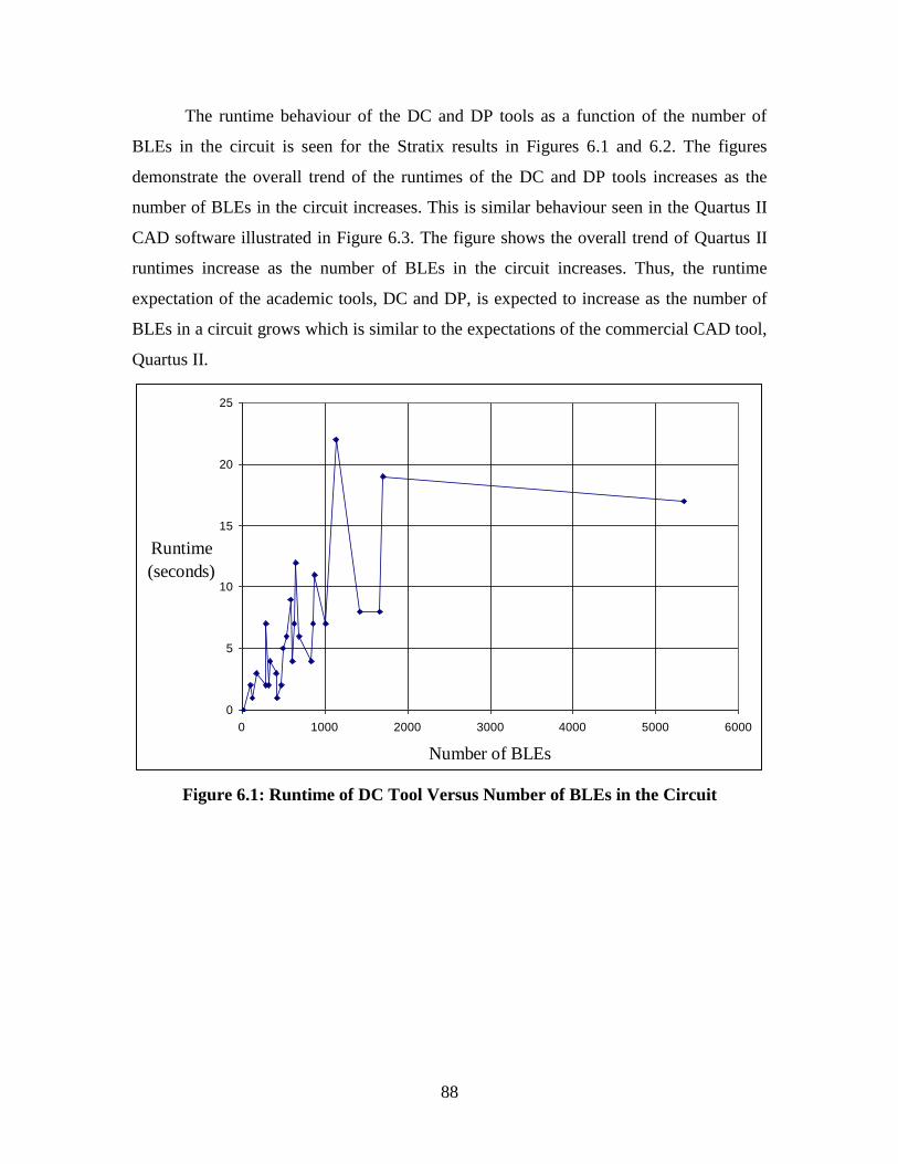
88
The runtime behaviour of the DC and DP tools as a function of the number of
BLEs in the circuit is seen for the Stratix results in Figures 6.1 and 6.2. The figures
demonstrate the overall trend of the runtimes of the DC and DP tools increases as the
number of BLEs in the circuit increases. This is similar behaviour seen in the Quartus II
CAD software illustrated in Figure 6.3. The figure shows the overall trend of Quartus II
runtimes increase as the number of BLEs in the circuit increases. Thus, the runtime
expectation of the academic tools, DC and DP, is expected to increase as the number of
BLEs in a circuit grows which is similar to the expectations of the commercial CAD tool,
Quartus II.
0
5
10
15
20
25
0 1000 2000 3000 4000 5000 6000
Number of BLEs
Runtime
(seconds)
Figure 6.1: Runtime of DC Tool Versus Number of BLEs in the Circuit

89
0
100
200
300
400
500
600
700
800
0 1000 2000 3000 4000 5000 6000
Number of BLEs
Runtime
(seconds)
Figure 6.2: Runtime of DP Tool Versus Number of BLEs in the Circuit
0
5
10
15
20
25
30
35
40
0 1000 2000 3000 4000 5000 6000
Number of BLEs
Runtime
(seconds)
Figure 6.3: Runtime of Quartus II Versus Number of BLEs in the Circuit
The Fmax that can be achieved by the DC and DP tools as a function of the number
of BLEs in the circuit is seen for the Stratix results in Figure 6.4. The figure shows no
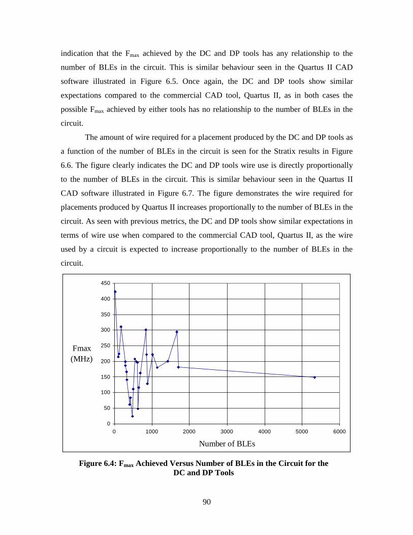
90
indication that the Fmax achieved by the DC and DP tools has any relationship to the
number of BLEs in the circuit. This is similar behaviour seen in the Quartus II CAD
software illustrated in Figure 6.5. Once again, the DC and DP tools show similar
expectations compared to the commercial CAD tool, Quartus II, as in both cases the
possible Fmax achieved by either tools has no relationship to the number of BLEs in the
circuit.
The amount of wire required for a placement produced by the DC and DP tools as
a function of the number of BLEs in the circuit is seen for the Stratix results in Figure
6.6. The figure clearly indicates the DC and DP tools wire use is directly proportionally
to the number of BLEs in the circuit. This is similar behaviour seen in the Quartus II
CAD software illustrated in Figure 6.7. The figure demonstrates the wire required for
placements produced by Quartus II increases proportionally to the number of BLEs in the
circuit. As seen with previous metrics, the DC and DP tools show similar expectations in
terms of wire use when compared to the commercial CAD tool, Quartus II, as the wire
used by a circuit is expected to increase proportionally to the number of BLEs in the
circuit.
0
50
100
150
200
250
300
350
400
450
0 1000 2000 3000 4000 5000 6000
Number of BLEs
Fmax
(MHz)
Figure 6.4: Fmax Achieved Versus Number of BLEs in the Circuit for the
DC and DP Tools

91
0
50
100
150
200
250
300
350
400
450
0 1000 2000 3000 4000 5000 6000
Number of BLEs
Fmax
(MHz)
Figure 6.5: Fmax Achieved Versus Number of BLEs in the Circuit for
Quartus II CAD Software
0
10000
20000
30000
40000
50000
60000
70000
0 1000 2000 3000 4000 5000 6000
Number of BLEs
Wire
Figure 6.6: Amount of Wire Required Versus Number of BLEs in the Circuit for the
DC and DP Tools

92
0
5000
10000
15000
20000
25000
30000
35000
40000
45000
50000
0 1000 2000 3000 4000 5000 6000
Number of BLEs
Wire
Figure 6.7: Amount of Wire Required Versus Number of BLEs in the Circuit for
Quartus II CAD Software
The results achieved demonstrate the flexibility of the DC and DP tools to target
different FPGA families, and provides performance similar to a commercial CAD tool.
The DC and DP tools’ results are within 10% of the Fmax achieved by Quartus II, and
results in less wire use. Further more, the behaviour of Fmax, wire used, and runtimes of
the DC and DP tools as the number of BLEs increase in a circuit is similar to what is seen
in a commercial CAD tool, Quartus II.
6.3 ALGORITHM EXPERIMENTS
Having shown that the DC and DP tools perform reasonably close to a
commercial tool, we show in this section examples of two experiments that can be
performed using our tools. The first experiment investigates the impact of clustering carry
chains. The second experiment investigates the impact of cluster sizes. These experiments
are presented as examples on how the tools can be used in an academic setting.

93
6.3.1 EXPERIMENT ONE: INVESTIGATE CLUSTERING
CARRY CHAINS
This experiment will compare clustering BLEs in carry chain formation in
isolation versus clustering BLEs in carry chain formation with other BLEs. This
experiment can be performed due to the DC tools’ ability to cluster a subset of BLEs in
different clustering attempts. As discussed in Section 3.8, the DC tool’s flexible
clustering ability allows us to investigate if BLEs in carry chain formation should be
clustered with only blocks in the same carry chain formation or clustered with other
BLEs in the circuit. Clustering BLEs in carry chain formation with other BLEs in the
circuit implies that the clustered blocks at that start or end of a carry chain formation may
include BLEs that are not part of the carry chain.
METHODOLOGY
This experiment will only be tested using circuits in the benchmarks set that have
carry chains formations. The circuits will only be tested on the Stratix device using the
DC flow described in Chapter 5. The investigation will evaluate clustering results using
two flows:
Flow 1: Clustering carry chains separately from other BLEs in the circuit.
Flow 2: Clustering carry chains with other BLEs in the circuit.
The methodology used to obtain the results will follow what was described in Chapter 5.
IMPLEMENTATION
This experiment can easily be attempted with the current clustering capability of
the DC tool. The tool is capable of targeting a subset of the BLEs in the circuit in each
clustering attempt as described in Chapter 3.
In flow 1, the DC tool will perform two clustering attempts. In the first clustering
attempt, the DC tool will only cluster BLEs in carry chain formation; and in the second
clustering attempt, the DC tool will cluster the remaining BLEs in the circuit which will
only consist of BLEs not in carry chain formations. For flow 1, the DC tool will have

94
created clustered blocks that will either be made up entirely of BLEs that are part of a
carry chain formation or made up of BLEs not in a carry chain formation.
For flow 2, the DC tool will cluster all the BLEs in the circuit in the same
clustering attempt allowing the possibility of BLEs in carry chain formation and BLEs
not in carry chain formations to be clustered in the same clustered block.
RESULTS
Table 6.6 summarizes the results of the clustering carry chains in isolation,
specified as flow 1, and clustering BLEs in carry chains with other BLEs in the circuit,
specified as flow 2. The table illustrates a minor benefit of clustering carry logic with
other logic as it improves the Fmax achieved by an average of 1.7% and reduces the wire
required to route the circuit by an average of 2.0%. The performance improvement seen
in flow 2 in both Fmax and wire used occurs since clustering the circuit in one attempt
gives the DC tool the most flexibility when creating clustered blocks. Since the runtimes
of the DC tool average about five seconds, the difference in runtime seen is insignificant.
Circuit
Fmax Wire
Flow 1 Flow 2 Flow 2 /
Flow 1
Flow 1 Flow 2 Flow 2 /
Flow 1
fip_cordic_rca 82.6 82.4 99.9% 5014.7 5098.7 101.7%
nut_000 44.9 47.0 104.6% 6149.3 5413.3 88.0%
nut_002 104.7 112.6 107.5% 4413.3 4433.3 100.5%
nut_004 144.8 146.0 100.8% 3078.7 2442.7 79.3%
oc_ata_ocidec1 239.0 248.5 104.0% 5704.0 5212.0 91.4%
oc_ata_ocidec2 235.5 213.5 90.7% 5989.3 6728.0 112.3%
oc_ata_v 234.4 239.0 101.9% 3394.7 3936.0 115.9%
oc_cordic_p2r 217.0 231.3 106.6% 9834.7 9652.0 98.1%
oc_cordic_r2p 210.7 220.8 104.8% 14240.0 13200.0 92.7%
oc_correlator 21.8 21.2 97.5% 4194.7 2992.0 71.3%
oc_i2c 195.7 194.3 99.3% 2424.0 2868.0 118.3%
oc_video_compression_
systems_huffman_dec 115.5 118.5 102.6% 7789.3 7910.7 101.6%
oc_video_compression_
systems_huffman_enc 204.8 209.1 102.1% 4212.0 4350.7 103.3%
Average 101.7% 98.0%
Table 6.6: Comparing Clustering BLEs in Carry Chains in Isolation (Flow 1) versus
Clustering BLEs in Carry Chains with Other Logic (Flow 2)

95
6.3.2 EXPERIMENT TWO: SPREAD-OUT CLUSTERING
This experiment will investigate if there is a benefit to create clustered blocks
without filling each cluster to its full capacity. This will provide the DC tool with
additional flexibility since it can now group the BLEs into a larger set of clusters. The
process of allowing BLEs to cluster in a larger number of clusters than the minimum
required is referred to as Spread-Out Clustering.
Spread-Out Clustering will decrease the chance that there will be unrelated BLEs
packed together just to fill up the entire cluster. This in turn should provide a benefit for
the placement algorithm to determine the optimal positions of these spread-out clusters. A
clustered block with two unrelated groups of BLEs will be attracted to different clusters
in the circuit and would like to be placed in different positions on the FPGA. A clustered
block that only contains BLEs with similar connections to other clustered blocks will
most likely find a more optimal placement of this cluster since all the BLEs in the cluster
will want to be placed near the same set of clustered blocks.
Spread-Out Clustering will also help the placement algorithm by reducing the
amount of routing congestion in each section of the FPGA since each cluster has a
reduced number of BLEs that will require fewer routing connections. Reducing routing
congestion on the FPGA will increase the chance each connection can be routed using the
shortest path on the FPGA.
METHODOLOGY
This experiment will only be tested using circuits in the benchmark set that do not
have carry chains. Circuits with carry chains do not benefit from Spread-Out Clustering
because it is always beneficial to place all of the BLEs in the carry chain in as few
clusters as possible. The experiment will only be tested on the Stratix device using the
DC flow described in Chapter 5. This investigation will evaluate the clustering results of
Spread-Out Clustering and the default clustering results obtained in the original DC flow
described in Section 6.2.1. The methodology used to obtain the results will follow what
was described in Chapter 5.

96
IMPLEMENTATION
This experiment was implemented by adding two new parameters to the DC tool
that can alter the cost function that determines if a BLE should be added to the current
cluster.
The first parameter provided allows the user to specify the minimum number of
BLEs within a spread-out cluster (MIN_SIZE). This parameter ensures that the DC tool
will not be prevented from adding BLEs to a small cluster. Altering the cluster size will
result in a tradeoff between the following two issues:
1. Smaller cluster sizes will give the placement algorithm a better chance to find an
optimal position for each clustered block on the FPGA
2. A smaller cluster size will generate a larger number of clustered blocks which in
turn make the placement problem more difficult since there will be a larger set of
clustered blocks that need to be placed.
This parameter allows the user to investigate the trade off between these conflicting
results that Spread-Out Clustering generates.
The second parameter provided allows the user to specify the minimum gain
(MIN_GAIN) that allows a BLE to be added to a cluster above the minimum number
(MIN_SIZE) specified. This minimum gain is determined by how much attraction the
BLE has to the other BLEs already in the clustered block. This value is normalized
between 0 and 1.0 with 0 implying no attraction to the current clustered block and 1.0
implying a strong attraction. The MIN_GAIN parameter allows Spread-Out Clustering to
cluster to capacity if the BLEs added to fill up the cluster has the specified minimum gain
that will benefit the cluster to include this BLE.
This experiment investigated a wide range of values for each parameter to
determine a configuration that provided the most benefit of the Spread-Out Clustering
process. The selected parameter values investigated in this experiment are specified in
Table 6.7.
Parameter Values
MIN_SIZE 7, 8, 9
MIN_GAIN 0.0 (default), 0.01, 0.2, 0.4, 0.6, 0.8, 1.0
Table 6.7: Parameter Values that were Investigated for Spread-Out Clustering

97
RESULTS
Table 6.8 summarizes the results of Spread-Out Clustering in the various
permutations specified from Table 6.7. Figure 6.8 displays an Fmax improvement curve
for each MIN_SIZE value across all the MIN_GAIN values investigated. The results
show that Spread-Out Clustering has a small benefit.
The results also show that the amount of wire used increases as the MIN_GAIN is
increased for each MIN_SIZE value. This is expected since higher MIN_GAIN values
result in a larger number of clustered blocks. The larger number of clusters creates an
increase in routing demand.
The affect on Fmax is illustrated in Figure 6.8. It shows that increasing the
MIN_GAIN above 0 increases Fmax but only to a certain point after which Fmax decreases.
Since the runtimes of the DC tool average about five seconds, the difference in runtime
seen is insignificant.
Considering both Fmax and wire results, setting the parameters MIN_SIZE to 7 and
MIN_GAIN to 0.2 seems to be a good tradeoff point as it achieved an Fmax improvement
of 1.5% with an increase in the amount of wire required to route the circuit by 3.5%
compared to the original clustering results.
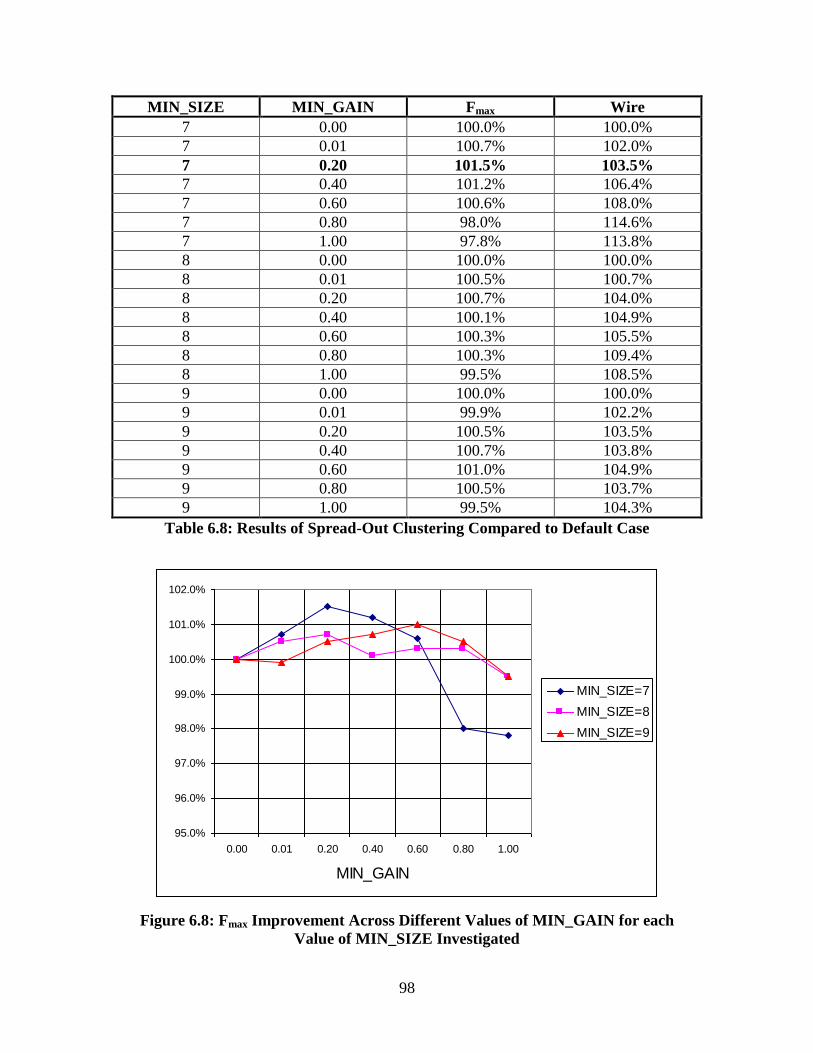
98
MIN_SIZE MIN_GAIN Fmax Wire
7 0.00 100.0% 100.0%
7 0.01 100.7% 102.0%
7 0.20 101.5% 103.5%
7 0.40 101.2% 106.4%
7 0.60 100.6% 108.0%
7 0.80 98.0% 114.6%
7 1.00 97.8% 113.8%
8 0.00 100.0% 100.0%
8 0.01 100.5% 100.7%
8 0.20 100.7% 104.0%
8 0.40 100.1% 104.9%
8 0.60 100.3% 105.5%
8 0.80 100.3% 109.4%
8 1.00 99.5% 108.5%
9 0.00 100.0% 100.0%
9 0.01 99.9% 102.2%
9 0.20 100.5% 103.5%
9 0.40 100.7% 103.8%
9 0.60 101.0% 104.9%
9 0.80 100.5% 103.7%
9 1.00 99.5% 104.3%
Table 6.8: Results of Spread-Out Clustering Compared to Default Case
95.0%
96.0%
97.0%
98.0%
99.0%
100.0%
101.0%
102.0%
0.00 0.01 0.20 0.40 0.60 0.80 1.00
MIN_GAIN
MIN_SIZE=7
MIN_SIZE=8
MIN_SIZE=9
Figure 6.8: Fmax Improvement Across Different Values of MIN_GAIN for each
Value of MIN_SIZE Investigated

99
7 CONCLUSIONS AND FUTURE WORK
7.1 CONTRIBUTIONS
This dissertation presented the clustering and placement capabilities of two new
tools, DC and DP. Chapter 3 and Chapter 4 discuss the flexibility of the DC and DP tools
to model a wide range of FPGA architectures, including commercial FPGA architectures.
Chapter 6 further shows the flexibility of the DC and DP tools by modeling Altera’s
Stratix and Cyclone FPGA architectures in a series of experiments.
The ability of the DC tool to model modern FPGA architectures required
developing a new constraint language, developing a new language to describe an FPGA
architecture, updated the algorithms within the DC tool to be configurable, and clustering
BLEs in carry chain formations. Similarly the DP tool required developing a new
language to define the FPGA architecture, updating the algorithms in the DP tool to be
configurable, and adding the ability to place BLEs in carry chain formations. The
flexibility of the DC and DP tools provides the ability to target real FPGA devices and
variants of real FPGAs.
Chapter 6 further illustrates the clustering and placement produced by the DC and
DP tools is at a level comparable to that of a commercial CAD tool, Quartus II, in both
the Fmax achieved and the amount of wire used to route the circuit. The experiments
investigated in Chapter 6 demonstrate the practical usefulness of the tools for future
academic FPGA research. The DC and DP tools provide future academic studies the
means to model a wider range of FPGA architectures, including commercial FPGA
architectures, in pursuit of investigating FPGA architectures features and algorithms for
FPGA CAD tools.

100
7.2 FUTURE WORK
The code for the DC and DP tools and the complete testing infrastructure used to
obtain the results in this dissertation will be available for future academic studies of
FPGA architectures and FPGA CAD tools. Numerous clustering and placement
suggestions for the advancement of the DC and DP tools were discussed in Section 3.10.3
and Section 4.9.3 respectively.
One benefit of adding the functionality mention in these sections is it will allow
the user to expand the benchmark set with circuits that have complex block types such as
memory blocks, multiplication blocks, and architectures with multiple K-LUT sizes. The
current set of circuits in the benchmark were selected from a set of circuits provided by
[15]. Many of the circuits available were excluded from the benchmark set because they
used complex block types.
Performing the routing step in the FPGA CAD flow is another functionality that
can be added to the DP tool. Currently, the DP tool routing algorithms that were inherited
from the original tool, VPR, is currently disabled and have not been updated with recent
changes made to the DP tool. Updating the router in the DP tool will provide another area
of FPGA CAD research to the user.
The DC and DP tools can be further upgraded in the future to cover an even wider
range of architectures as new architectures develop. This will allow academic studies to
keep up with recent technology trends in industry and be able to provide relevant results
in their research projects. Upgrading the academic tools used to study FPGA architectures
will allow future projects to cover a wider range of architectures and provide more
relevant results.

101
8 REFERENCES
[1] R. Jayaraman, ―Physical design for FPGAs,‖ Proceedings of the 2001 International
Symposium on Physical Design, April 2001, pp. 214-221.
[2] V. Betz, J. Rose, and A. Marquardt, Architecture and CAD for Deep-Submicron
FPGAs. Norwell, MA: Kluwer Academic Publishers. 1999.
[3] A. Marquardt, V. Betz, J. Rose, "Using Cluster-Based Logic Blocks and Timing-
Driven Packing to Improve FPGA Speed and Density," Proceedings of the 1999
ACM/SIGDA Seventh International Symposium on Field Programmable Gate
Arrays, February 1999, pp.37-46.
[4] V. Betz, J. Rose, ―Automatic Generation of FPGA Routing Architectures from
High-Level Descriptions,‖ Proceedings of the 2000 ACM/SIGDA Eighth
International Symposium on Field Programmable Gate Arrays, February 2000,
pp.175-184.
[5] A. Singh, G. Parthasarathy, M. Marek-Sadowska, ―Efficient Circuit Clustering for
Area and Power Reduction in FPGAs,‖ ACM Transactions on Design Automation
of Electronic Systems (TODAES), Vol. 7, October 2002, pp.643-663.
[6] Y. Sankar, J. Rose, ―Trading Quality for Compile Time: Ultra-Fast Placement for
FPGAs,‖ Proceedings of the 1999 ACM/SIGDA Seventh International Symposium
on Field Programmable Gate Arrays, February 1999, pp.157-166.
[7] J. S. Swartz, V. Betz, J. Rose, ―A Fast Routability-Driven Router for FPGAs‖,
Proceedings of the 1998 ACM/SIGDA Sixth International Symposium on Field
Programmable Gate Arrays, February 1998, pp.140-149.
[8] J. He, ―Technology Mapping and Architecture of Heterogeneous Field-
Programmable Gate Arrays,‖ M.A.Sc. Thesis, University of Toronto, 1993.
[9] P. Jamieson, J. Rose, "A Verilog RTL Synthesis Tool For Heterogeneous FPGAs,"
Proceedings of the 2005 International Conference on Field Programmable Logic
and Applications (FPL'05), August 2005, pp. 305-310.

102
[10] V. Betz, VPR and T-VPack User's Manual (Version 4.30), 2000.
―http://www.eecg.toronto.edu/~vaughn/vpr/vpr.html‖, January 2008.
[11] S. D. Brown, J. Rose, Z. G. Vranesic, ―A Detailed Router for Field-Programmable
Gate Arrays,‖ in IEEE Transactions on Computer-Aided Design, Vol. II, No. 5,
May 1992, pp. 620-628.
[12] N. Weste, D Harris, CMOS VLSI Design: A Circuits and Systems Perspective 3rd
ed. Boston, MA: Pearson Education, Inc. 2005.
[13] D. Lewis, V. Betz, D. Jefferson, A. Lee, C. Lane, P. Leventis, S. Marquardt, C.
McClintock, B. Pedersen, G. Powell, S. Reddy, C. Wysocki, R. Cliff, J. Rose, ―The
Stratix Routing and Logic Architecture,‖ Proceedings of the 2003 ACM/SIGDA
International Symposium on Field-Programmable Gate Arrays, February 2003, pp.
12-20.
[14] V. Betz and J. Rose, ―Cluster-Based Logic Blocks for FPGAs: Area-Efficiency vs.
Input Sharing and Size,‖ IEEE Custom Integrated Circuits Conference, Santa Clara,
CA, 1997, pp. 551-554.
[15] Altera’s Quartus II University Interface Program,
―http://www.altera.com/education/univ/research/unv-quip.html‖, January 2008.
[16] D. Lewis, E. Ahmed, G. Baeckler, V. Betz, M. Bourgeault, D. Cashman, D.
Galloway, M. Hutton, C. Lane, A. Lee, P. Leventis, S. Marquardt, C. McClintock,
K. Padalia, B. Pedersen, G. Powell, B. Ratchev, S. Reddy, J. Schleicher, K. Stevens,
R. Yuan, R. Cliff, J. Rose, ―The Stratix II Logic and Routing Architecture,‖ in
FPGA '05, ACM Symposium on FPGAs, February 2005, pp 14-20.
[17] P. Chow, S. Seo, J. Rose, K. Chung, I Rahardja, G. Paez, ―The Design of an SRAM-
Based Field-Programmable Gate Array: Part II: Circuit Design and Layout,‖ in
IEEE Transactions on VLSI, Vol. 7, No. 3, September 1999, pp. 321-330.
[18] A. Dunlop, B. Kernighan, ―A Procedure for Placement of Standard-Cell VLSI
Circuits,‖ in IEEE Transactions on CAD, January 1985, pp. 92-98.
[19] D. Huang, A. Kahng, ―Partitioning-Based Standard-Cell Global Placement with an
Exact Objective,‖ in ACM Symposium on Physical Design, 1997, pp. 18-25.

103
[20] G. Sigl, K. Doll, F. Johannes, ―Analytical Placement: A Linear or a Quadratic
Objective Function?,‖ DAC, 1991, pp. 427-432.
[21] B. Riess, G. Ettelt, ―Speed: Fast and Efficient Timing Driven Placement,‖ in IEEE
International Symposium on Circuits and Systems, 1995, pp. 377-380.
[22] W. Sun, C. Sechen, ―Efficient and Effective Placement for Very Large Circuits,‖ in
IEEE Transactions on CAD, March 1995, pp. 349-359.
[23] W. Swartz, C. Sechen, ―Timing Driven Placement for Large Standard Cell
Circuits,‖ DAC, 1995, pp. 211-215.
[24] V. Betz, J. Rose, "VPR: A New Packing, Placement and Routing Tool for FPGA
Research," in 7th International Workshop on Field-Programmable Logic, Londan,
August 1997, pp. 213-222.
[25] T. Czajkowski, ―Physical Synthesis Toolkit for FPGAs,‖ Ph.D. Thesis, University of
Toronto, in preparation.
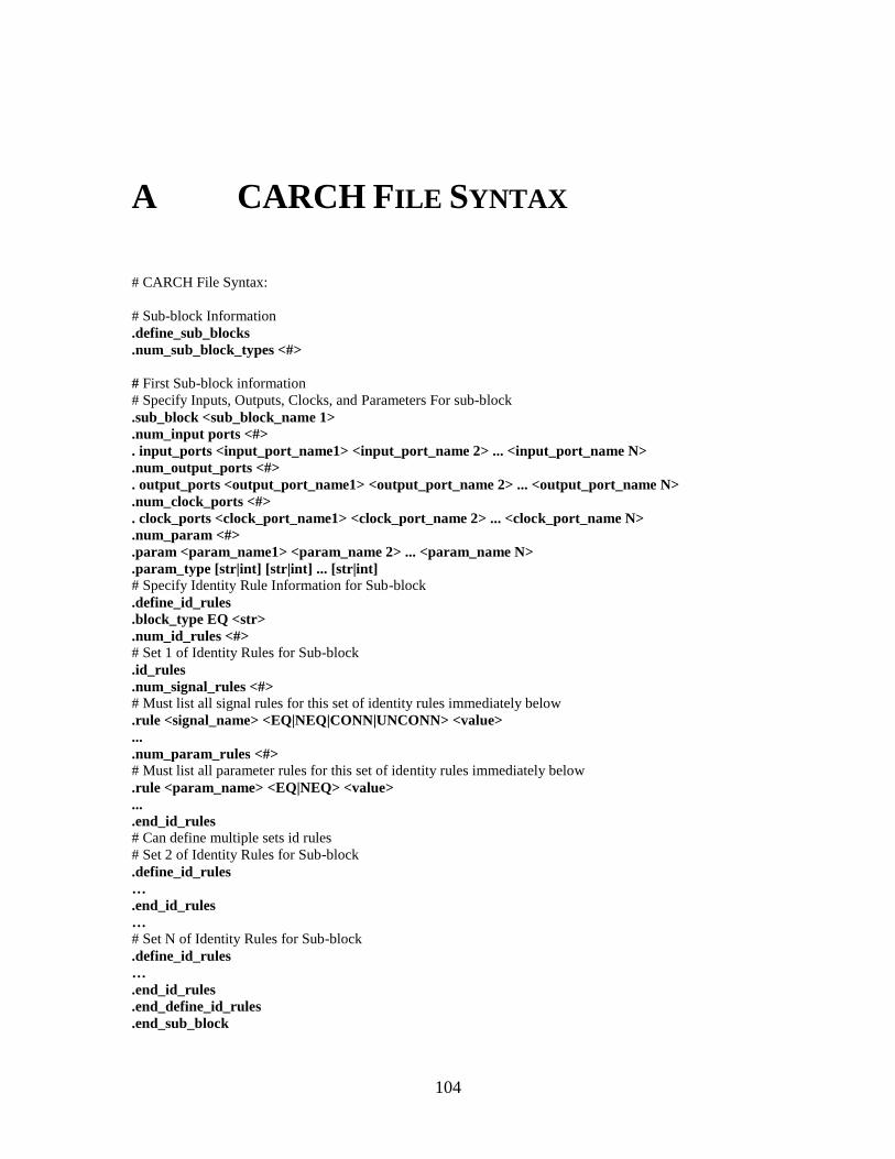
104
A CARCH FILE SYNTAX
# CARCH File Syntax:
# Sub-block Information
.define_sub_blocks
.num_sub_block_types <#>
# First Sub-block information
# Specify Inputs, Outputs, Clocks, and Parameters For sub-block
.sub_block <sub_block_name 1>
.num_input ports <#>
. input_ports <input_port_name1> <input_port_name 2> ... <input_port_name N>
.num_output_ports <#>
. output_ports <output_port_name1> <output_port_name 2> ... <output_port_name N>
.num_clock_ports <#>
. clock_ports <clock_port_name1> <clock_port_name 2> ... <clock_port_name N>
.num_param <#>
.param <param_name1> <param_name 2> ... <param_name N>
.param_type [str|int] [str|int] ... [str|int]
# Specify Identity Rule Information for Sub-block
.define_id_rules
.block_type EQ <str>
.num_id_rules <#>
# Set 1 of Identity Rules for Sub-block
.id_rules
.num_signal_rules <#>
# Must list all signal rules for this set of identity rules immediately below
.rule <signal_name> <EQ|NEQ|CONN|UNCONN> <value>
...
.num_param_rules <#>
# Must list all parameter rules for this set of identity rules immediately below
.rule <param_name> <EQ|NEQ> <value>
...
.end_id_rules
# Can define multiple sets id rules
# Set 2 of Identity Rules for Sub-block
.define_id_rules
…
.end_id_rules
…
# Set N of Identity Rules for Sub-block
.define_id_rules
…
.end_id_rules
.end_define_id_rules
.end_sub_block

105
# Can define multiple sub_blocks
# Second Sub-block information
sub_block <sub_block_name 2>
…
.end_sub_block
…
# Nth
Sub-block information
sub_block <sub_block_name N>
…
.end_sub_block
.end_define_sub_blocks
# Block Information
.define_blocks
.num_block_types <#>
# 1st Block Information
# Specify inputs, outputs, which outputs are registered, clock, parameter information, and sub-block info
.block <name 1>
.num_input_ports <#>
.input_ports <input_port_name1> <input_port_name 2> ... <input_port_name N>
.num_output_ports <#>
. output_ports <output_port_name1> <output_port_name 2> ... <output_port_name N> # To specify if each output is registered: yes =1 and no = 0
.is_output_port_reg <0|1> <0|1> ... <0|1>
.num_clock_ports <#>
. clock_ports <clock_port_name1> <clock_port_name 2> ... <clock_port_name N>
.num_param <#>
.param <param_name1> <param_name 2> ... <param_name N>
.num_max_sub_blocks <#>
# Specify Identity Rule Information for Block
.define_id_rules
.num_id_rules <#>
# Set 1 of Identity Rules for Block 1
.id_rules
.block_type EQ <str>
.num_signal_rules <#>
# Must list all signal rules for this set of identity rules immediately below
.rule <signal_name> <EQ|NEQ|CONN|UNCONN> <value>
...
.num_param_rules <#>
# Must list all parameter rules for this set of identity rules immediately below
.rule <param_name> <EQ|NEQ> <value>
...
.end_id_rules
# Can define multiple sets id rules
# Set 2 of Identity Rules for Block
.define_id_rules
…
.end_id_rules
…
# Set N of Identity Rules for Block
.define_id_rules
…
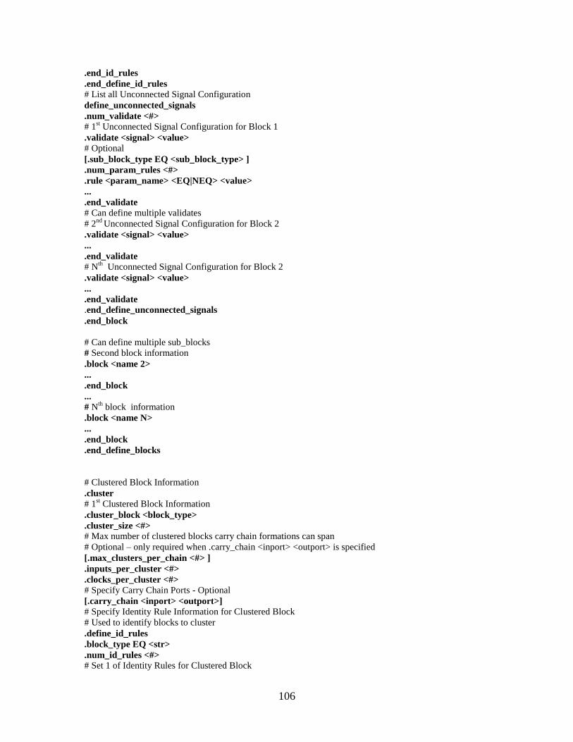
106
.end_id_rules
.end_define_id_rules
# List all Unconnected Signal Configuration
define_unconnected_signals
.num_validate <#>
# 1st Unconnected Signal Configuration for Block 1
.validate <signal> <value>
# Optional
[.sub_block_type EQ <sub_block_type> ]
.num_param_rules <#>
.rule <param_name> <EQ|NEQ> <value>
...
.end_validate
# Can define multiple validates
# 2nd
Unconnected Signal Configuration for Block 2
.validate <signal> <value>
...
.end_validate
# Nth
Unconnected Signal Configuration for Block 2
.validate <signal> <value>
...
.end_validate
.end_define_unconnected_signals
.end_block
# Can define multiple sub_blocks
# Second block information
.block <name 2>
...
.end_block
...
# Nth
block information
.block <name N>
...
.end_block
.end_define_blocks
# Clustered Block Information
.cluster
# 1st Clustered Block Information
.cluster_block <block_type>
.cluster_size <#>
# Max number of clustered blocks carry chain formations can span
# Optional – only required when .carry_chain <inport> <outport> is specified
[.max_clusters_per_chain <#> ]
.inputs_per_cluster <#>
.clocks_per_cluster <#>
# Specify Carry Chain Ports - Optional
[.carry_chain <inport> <outport>]
# Specify Identity Rule Information for Clustered Block
# Used to identify blocks to cluster
.define_id_rules
.block_type EQ <str>
.num_id_rules <#>
# Set 1 of Identity Rules for Clustered Block
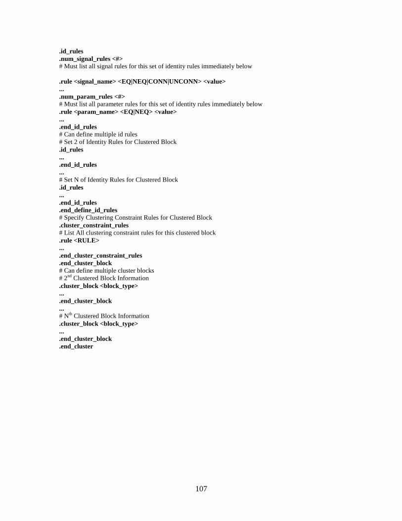
107
.id_rules
.num_signal_rules <#>
# Must list all signal rules for this set of identity rules immediately below
.rule <signal_name> <EQ|NEQ|CONN|UNCONN> <value>
...
.num_param_rules <#>
# Must list all parameter rules for this set of identity rules immediately below
.rule <param_name> <EQ|NEQ> <value>
...
.end_id_rules
# Can define multiple id rules
# Set 2 of Identity Rules for Clustered Block
.id_rules
...
.end_id_rules
...
# Set N of Identity Rules for Clustered Block
.id_rules
...
.end_id_rules
.end_define_id_rules
# Specify Clustering Constraint Rules for Clustered Block
.cluster_constraint_rules
# List All clustering constraint rules for this clustered block
.rule <RULE>
...
.end_cluster_constraint_rules
.end_cluster_block
# Can define multiple cluster blocks
# 2nd
Clustered Block Information
.cluster_block <block_type>
...
.end_cluster_block
...
# Nth
Clustered Block Information
.cluster_block <block_type>
...
.end_cluster_block
.end_cluster

108
B CARCH FILE EXAMPLES
B.1 CARCH FILE USED TO MODEL STRATIX DEVICE
# stratix.carch
# Sub-block Information
.define_sub_blocks
.num_sub_block_types 2
# First Sub-block information (LUT)
.sub_block LUT
.num_input ports 6
. input_ports dataa datab datac datad cin inverta
.num_output_ports 2
. output_ports combout cout
.num_clock_ports 0
.num_param 6
.param operation_mode synch_mode register_cascade_mode sum_lutc_input lut_mask output_mode
.param_type str str str str str str
# Specify Identity Rule Information for Sub-block
.define_id_rules
.block_type EQ stratix_lcell
.num_id_rules 2
# Set 1 of Identity Rules for Sub-block
.id_rules
.num_signal_rules 0
.num_param_rules 1
.rule output_mode NEQ reg_only
.end_id_rules
# Set 2 of Identity Rules for Sub-block
.define_id_rules
.num_signal_rules 2
.rule sload NEQ VCC
.rule aload NEQ VCC
.num_param_rules 2
.rule output_mode EQ reg_only
.rule register_cascade_mode EQ off
.end_id_rules
.end_define_id_rules
.end_sub_block
# Second Sub-block information (Flip Flop)
.sub_block FF
.num_input ports 7
. input_ports datac aclr aload sclr sload ena regcascin
.num_output_ports 1
. output_ports regout

109
.num_clock_ports 1
. clock_ports clk
.num_param 6
.param operation_mode synch_mode register_cascade_mode sum_lutc_input lut_mask output_mode
.param_type str str str str str str
# Specify Identity Rule Information for Sub-block
.define_id_rules
.block_type EQ stratix_lcell
.num_id_rules 2
# Set 1 of Identity Rules for Sub-block
.id_rules
.num_signal_rules 0
.num_param_rules 2
.rule output_mode NEQ comb_only
.rule operation_mode EQ normal
.end_id_rules
# Set 2 of Identity Rules for Sub-block
.define_id_rules
.num_signal_rules 0
.num_param_rules 2
.rule output_mode EQ comb_only
.rule sum_lutc_input EQ qfbk
.end_id_rules
.end_define_id_rules
.end_sub_block
.end_define_sub_blocks
# Block Information
.define_blocks
.num_block_types 2
# 1st Block Information (BLE)
.block stratix_lcell
.num_input_ports 12
.input_ports dataa datab datac datad aclr aload sclr sload ena cin inverta regcascin
.num_output_ports 3
. output_ports combout regout cout
.is_output_port_reg 0 1 0
.num_clock_ports 1
.clock_ports clk
.num_param 6
.param operation_mode synch_mode register_cascade_mode sum_lutc_input lut_mask output_mode
.num_max_sub_blocks 2
# Specify Identity Rule Information for Block
.define_id_rules
.num_id_rules 1
# Set 1 of Identity Rules for Block 1
.id_rules
.block_type EQ stratix_lcell
.num_signal_rules 0
.num_param_rules 0
.end_id_rules
.end_define_id_rules
# List all Unconnected Signal Configuration
define_unconnected_signals
.num_validate 6
# 1st Unconnected Signal Configuration for Block

110
.validate aclr gnd
.sub_block_type EQ ff
.num_param_rules 0
.end_validate
# 2nd
Unconnected Signal Configuration for Block
.validate sload gnd
.sub_block_type EQ ff
.num_param_rules 1
.rule synch_mode EQ on
.end_validate
# 3rd
Unconnected Signal Configuration for Block
.validate sclr gnd
.sub_block_type EQ ff
.num_param_rules 1
.rule synch_mode EQ on
.end_validate
# 4th
Unconnected Signal Configuration for Block
.validate ena vcc
.sub_block_type EQ ff
.num_param_rules 0
.end_validate
# 5th
Unconnected Signal Configuration for Block
.validate clk gnd
.sub_block_type EQ ff
.num_param_rules 0
.end_validate
# 6th
Unconnected Signal Configuration for Block
.validate inverta gnd
.num_param_rules 0
.end_validate
.end_define_unconnected_signals
.end_block
# Second block information (I/O)
.block stratix_io
.num_input_ports 8
.input_ports datain ddiodatain oe outclkena inclkena areset sreset padio
.num_output_ports 3
. output_ports combout regout ddioregout
.is_output_port_reg 0 1 1
.num_clock_ports 2
.clock_ports outclk inclk
.num_param 14
.param operation_mode ddio_mode input_register_mode output_register_mode oe_register_mode \
input_async_reset output_async_reset oe_async_reset input_sync_reset output_sync_reset oe_sync_reset \
input_power_up output_power_up oe_power_up
.num_max_sub_blocks 0
# Specify Identity Rule Information for Block
.define_id_rules
.num_id_rules 1
# Set 1 of Identity Rules for Block 1
.id_rules
.block_type EQ stratix_io
.num_signal_rules 0
.num_param_rules 0
.end_id_rules
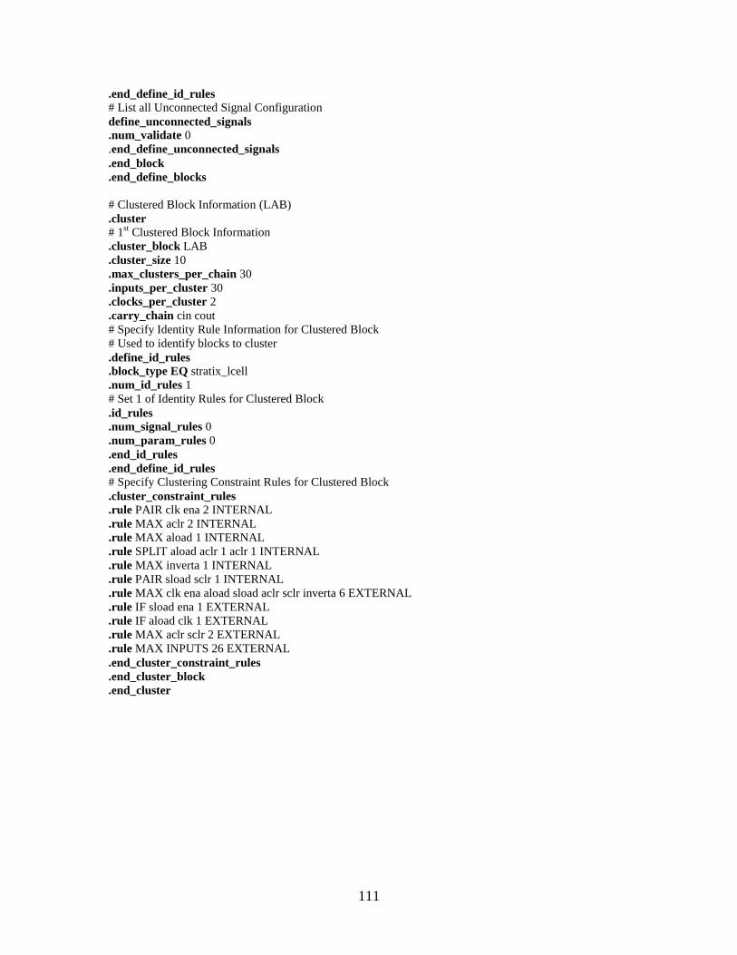
111
.end_define_id_rules
# List all Unconnected Signal Configuration
define_unconnected_signals
.num_validate 0
.end_define_unconnected_signals
.end_block
.end_define_blocks
# Clustered Block Information (LAB)
.cluster
# 1st Clustered Block Information
.cluster_block LAB
.cluster_size 10
.max_clusters_per_chain 30
.inputs_per_cluster 30
.clocks_per_cluster 2
.carry_chain cin cout
# Specify Identity Rule Information for Clustered Block
# Used to identify blocks to cluster
.define_id_rules
.block_type EQ stratix_lcell
.num_id_rules 1
# Set 1 of Identity Rules for Clustered Block
.id_rules
.num_signal_rules 0
.num_param_rules 0
.end_id_rules
.end_define_id_rules
# Specify Clustering Constraint Rules for Clustered Block
.cluster_constraint_rules
.rule PAIR clk ena 2 INTERNAL
.rule MAX aclr 2 INTERNAL
.rule MAX aload 1 INTERNAL
.rule SPLIT aload aclr 1 aclr 1 INTERNAL
.rule MAX inverta 1 INTERNAL
.rule PAIR sload sclr 1 INTERNAL
.rule MAX clk ena aload sload aclr sclr inverta 6 EXTERNAL
.rule IF sload ena 1 EXTERNAL
.rule IF aload clk 1 EXTERNAL
.rule MAX aclr sclr 2 EXTERNAL
.rule MAX INPUTS 26 EXTERNAL
.end_cluster_constraint_rules
.end_cluster_block
.end_cluster

112
B.2 CARCH FILE USED TO MODEL CYCLONE DEVICE
# cyclone.carch
# Sub-block Information
.define_sub_blocks
.num_sub_block_types 2
# First Sub-block information (LUT)
.sub_block LUT
.num_input ports 6
. input_ports dataa datab datac datad cin inverta
.num_output_ports 2
. output_ports combout cout
.num_clock_ports 0
.num_param 6
.param operation_mode synch_mode register_cascade_mode sum_lutc_input lut_mask output_mode
.param_type str str str str str str
# Specify Identity Rule Information for Sub-block
.define_id_rules
.block_type EQ stratix_lcell
.num_id_rules 2
# Set 1 of Identity Rules for Sub-block
.id_rules
.num_signal_rules 0
.num_param_rules 1
.rule output_mode NEQ reg_only
.end_id_rules
# Set 2 of Identity Rules for Sub-block
.define_id_rules
.num_signal_rules 2
.rule sload NEQ VCC
.rule aload NEQ VCC
.num_param_rules 2
.rule output_mode EQ reg_only
.rule register_cascade_mode EQ off
.end_id_rules
.end_define_id_rules
.end_sub_block
# Second Sub-block information (Flip Flop)
.sub_block FF
.num_input ports 7
. input_ports datac aclr aload sclr sload ena regcascin
.num_output_ports 1
. output_ports regout
.num_clock_ports 1
. clock_ports clk
.num_param 6
.param operation_mode synch_mode register_cascade_mode sum_lutc_input lut_mask output_mode
.param_type str str str str str str
# Specify Identity Rule Information for Sub-block
.define_id_rules
.block_type EQ stratix_lcell
.num_id_rules 2

113
# Set 1 of Identity Rules for Sub-block
.id_rules
.num_signal_rules 0
.num_param_rules 2
.rule output_mode NEQ comb_only
.rule operation_mode EQ normal
.end_id_rules
# Set 2 of Identity Rules for Sub-block
.define_id_rules
.num_signal_rules 0
.num_param_rules 2
.rule output_mode EQ comb_only
.rule sum_lutc_input EQ qfbk
.end_id_rules
.end_define_id_rules
.end_sub_block
.end_define_sub_blocks
# Block Information
.define_blocks
.num_block_types 2
# 1st Block Information (BLE)
.block stratix_lcell
.num_input_ports 12
.input_ports dataa datab datac datad aclr aload sclr sload ena cin inverta regcascin
.num_output_ports 3
. output_ports combout regout cout
.is_output_port_reg 0 1 0
.num_clock_ports 1
.clock_ports clk
.num_param 6
.param operation_mode synch_mode register_cascade_mode sum_lutc_input lut_mask output_mode
.num_max_sub_blocks 2
# Specify Identity Rule Information for Block
.define_id_rules
.num_id_rules 1
# Set 1 of Identity Rules for Block 1
.id_rules
.block_type EQ stratix_lcell
.num_signal_rules 0
.num_param_rules 0
.end_id_rules
.end_define_id_rules
# List all Unconnected Signal Configuration
define_unconnected_signals
.num_validate 6
# 1st Unconnected Signal Configuration for Block
.validate aclr gnd
.sub_block_type EQ ff
.num_param_rules 0
.end_validate
# 2nd
Unconnected Signal Configuration for Block
.validate sload gnd
.sub_block_type EQ ff
.num_param_rules 1
.rule synch_mode EQ on

114
.end_validate
# 3rd
Unconnected Signal Configuration for Block
.validate sclr gnd
.sub_block_type EQ ff
.num_param_rules 1
.rule synch_mode EQ on
.end_validate
# 4th
Unconnected Signal Configuration for Block
.validate ena vcc
.sub_block_type EQ ff
.num_param_rules 0
.end_validate
# 5th
Unconnected Signal Configuration for Block
.validate clk gnd
.sub_block_type EQ ff
.num_param_rules 0
.end_validate
# 6th
Unconnected Signal Configuration for Block
.validate inverta gnd
.num_param_rules 0
.end_validate
.end_define_unconnected_signals
.end_block
# Second block information (I/O)
.block stratix_io
.num_input_ports 8
.input_ports datain ddiodatain oe outclkena inclkena areset sreset padio
.num_output_ports 3
. output_ports combout regout ddioregout
.is_output_port_reg 0 1 1
.num_clock_ports 2
.clock_ports outclk inclk
.num_param 14
.param operation_mode ddio_mode input_register_mode output_register_mode oe_register_mode \
input_async_reset output_async_reset oe_async_reset input_sync_reset output_sync_reset oe_sync_reset \
input_power_up output_power_up oe_power_up
.num_max_sub_blocks 0
# Specify Identity Rule Information for Block
.define_id_rules
.num_id_rules 1
# Set 1 of Identity Rules for Block 1
.id_rules
.block_type EQ stratix_io
.num_signal_rules 0
.num_param_rules 0
.end_id_rules
.end_define_id_rules
# List all Unconnected Signal Configuration
define_unconnected_signals
.num_validate 0
.end_define_unconnected_signals
.end_block
.end_define_blocks
# Clustered Block Information (LAB)

115
.cluster
# 1st Clustered Block Information
.cluster_block LAB
.cluster_size 10
.max_clusters_per_chain 13
.inputs_per_cluster 30
.clocks_per_cluster 2
.carry_chain cin cout
# Specify Identity Rule Information for Clustered Block
# Used to identify blocks to cluster
.define_id_rules
.block_type EQ stratix_lcell
.num_id_rules 1
# Set 1 of Identity Rules for Clustered Block
.id_rules
.num_signal_rules 0
.num_param_rules 0
.end_id_rules
.end_define_id_rules
# Specify Clustering Constraint Rules for Clustered Block
.cluster_constraint_rules
.rule PAIR clk ena 2 INTERNAL
.rule MAX aclr 2 INTERNAL
.rule MAX aload 1 INTERNAL
.rule SPLIT aload aclr 1 aclr 1 INTERNAL
.rule MAX inverta 1 INTERNAL
.rule PAIR sload sclr 1 INTERNAL
.rule MAX clk ena aload sload aclr sclr inverta 6 EXTERNAL
.rule IF sload ena 1 EXTERNAL
.rule IF aload clk 1 EXTERNAL
.rule MAX aclr sclr 2 EXTERNAL
.rule MAX INPUTS 23 EXTERNAL
.end_cluster_constraint_rules
.end_cluster_block
.end_cluster

116
C EXAMPLE OF A CNET FILE
# ts_mike_fsm.cnet:
.global clock~combout
.constant gnd
.clb 1 clock~I
.mode 0
pinlist: open open open open open open open pin_con clock~combout open open open open
.clb 1 in[1]~I
.mode 0
pinlist: open open open open open open open pin_con in[1]~combout open open open open
.clb 1 in[0]~I
.mode 0
pinlist: open open open open open open open pin_con in[0]~combout open open open open
.clb 1 in[2]~I
.mode 0
pinlist: open open open open open open open pin_con in[2]~combout open open open open
.clb 1 in[3]~I
.mode 0
pinlist: open open open open open open open pin_con in[3]~combout open open open open
.clb 1 out[0]~I
.mode 1
pinlist: Select~640 open open open open open open pin_con open open open open open
.clb 1 out[1]~I
.mode 1
pinlist: reduce_or~15 open open open open open open pin_con open open open open open
.clb 1 out[2]~I
.mode 1
pinlist: Select~640 open open open open open open pin_con open open open open open
.clb 1 out[3]~I
.mode 1
pinlist: Select~641 open open open open open open pin_con open open open open open
.clb 1 out[4]~I
.mode 1
pinlist: Select~641 open open open open open open pin_con open open open open open
.clb 1 out[5]~I

117
.mode 1
pinlist: reduce_or~15 open open open open open open pin_con open open open open open
.clb 1 out[6]~I
.mode 1
pinlist: Select~643 open open open open open open pin_con open open open open open
.clb 1 out[7]~I
.mode 1
pinlist: Select~646 open open open open open open pin_con open open open open open
.clb 1 out[8]~I
.mode 1
pinlist: Select~643 open open open open open open pin_con open open open open open
.clb 1 out[9]~I
.mode 1
pinlist: gnd open open open open open open pin_con open open open open open
.clb 0 Select~638_I
.mode 0
pinlist: in[1]~combout in[0]~combout in[2]~combout in[3]~combout reduce_or~15 gnd Select~645 open
open open open open open open open open open open open open open open open open open open open
open open open open open open open open open open current_state.000 open open open open open open
open open open open Select~640 open open Select~641 open open open open open Select~643 open open
clock~combout open
subblock: 0 0 Select~638_I 0 1 2 3 open open open open open open open open 30 open open open
subblock: 0 0 next_state.010~66_I 1 2 0 3 open open open open open open open open 33 open open open
subblock: 0 0 current_state.000~I 4 open open open 5 open open open open open open open open 37 open
60
subblock: 0 0 current_state.010~I ble_1_0 ble_4_1 1 ble_2_1 5 open open open open open open open open
40 open 60
subblock: 0 0 current_state.101~I ble_3_1 open ble_2_1 6 5 open open open open open open open open 43
open 60
subblock: 0 0 Select~639_I ble_4_1 ble_3_1 ble_2_1 2 open open open open open open open open 45 open
open open
subblock: 0 0 Select~640_I ble_0_0 ble_5_0 ble_1_0 open open open open open open open open open 48
open open open
subblock: 0 0 Select~641_I 1 ble_2_1 open ble_1_0 open open open open open open open open 51 open
open open
subblock: 0 0 Select~642_I 2 ble_4_1 0 1 open open open open open open open open 54 open open open
subblock: 0 0 Select~643_I 3 ble_8_0 ble_3_1 1 open open open open open open open open 57 open open
open
.clb 0 reduce_or~15_I
.mode 0
pinlist: in[0]~combout in[1]~combout in[2]~combout in[3]~combout current_state.000 open open open
open open open open open open open open open open open open open open open open open open open
open open open reduce_or~15 open open Select~645 open open open open open Select~646 open open
open open open open open open open open open open open open open open open open open open open
open
subblock: 0 0 reduce_or~15_I 0 1 2 3 open open open open open open open open 30 open open open
subblock: 0 0 Select~645_I 1 0 2 3 open open open open open open open open 33 open open open
subblock: 0 0 Select~644_I 0 1 2 3 open open open open open open open open 36 open open open
subblock: 0 0 Select~646_I ble_2_0 4 ble_1_0 open open open open open open open open open 39 open
open open

118
D PARCH FILE SYNTAX
# Specify General Chip Info
.chip_info
chan_width_io <#>
chan_width_x uniform <#>
chan_width_y uniform <#>
num_block_types <#>
num_sub_block_types <#>
# note: nx, ny is upper bound - lower bound assumed to be 0,0
nx <#>
ny <#>
.end_chip_info
# Define Block – example how to specify a block (Clustered Block) that contain sub-blocks (BLEs)
.define_block_type <block_name>
# Specify Block Information
.block_info
num_loc <#>
pins_per_clb <#>
# non clock/global inputs
num_inputs <#>
num_outputs <#>
num_inter_nodes <#>
num_pin_classes <#>
num_pins_in_each_class <# > <#> … <#>
.end_block_info
# Specify block pin information for each block pin specified above for block
.block_pins
# For each class need to
inpin class: <class_number> [top|bottom|left|right]
…
outpin class: <class_number> [top|bottom|left|right]
…
inpin class: <class_number> global [top|bottom|left|right]
…
.end_block_pins
# Specify internal Delays for a block
# This is specific for Blocks (Clustered blocks) that contain sub-blocks (BLEs)
.block_delays
# 0 means no modes - since sub blocks will be configured with modes
num_modes 0
# the following 3 commands are only specified when the block has no modes since the block has sub blocks
# These commands specify the delays from the block to the sub-blocks
T_sblk_opin_to_sblk_ipin <#>
T_clb_ipin_to_sblk_ipin <#>
T_sblk_opin_to_clb_opin <#>

119
.end_block_delays
# Sub-block Info
# Only required when block (Clustered blocks) contains Sub-blocks (BLEs)
.sub_block_info
sub_blocks_per_clb <#>
.end_sub_block_info
# Locations block is found on FPGA
.block_loc
.max_occ 1
# Each ―range‖ command specifies a range on the FPGA where this block can be found that can
# span multiple columns and multiple rows
range # # to # #
range # # to # #
…
# Each ―line‖ command specifies positions within a column/row on the FPGA where this block is found
line [x|y] <#> [x|y] <#> <#> … <#>
line [x|y] <#> [x|y] <#> <#> … <#>
…
.end_max_occ
# Can specify multiple max occupancy groups
.max_occ <#>
…
.end_max_occ
.end_block_loc
.end_define_block_type
# Specify sub block information
# Needed for blocks (Clustered blocks) that contain sub-blocks (BLE)
.define_sub_block_type <sub_block_name>
# Specify Sub-Block Information
.sub_block_pin_info
sub_block_inputs <#>
sub_block_outputs <#>
sub_block_clk_inputs <#>
sub_block_inter_nodes <#>
sub_block_port_names <name_1> <name_2> … <name_N>
.end_sub_block_pin_info
# Specify internal Delays for the sub-block (BLE)
.sub_block_delays
# num of modes will be at least 1 since this is a sub-block
# More than 1 implies the sub-block has multiple timing models for diff modes
num_modes <#>
# Specifying Timing sub-block delay model for 1st sub-block mode
.mode
.delay_info
# Specify delays for connections between all inputs, outputs, and intermediate nodes.
# -1.0 implies no connection between specified input/output/intermediate node and
# input/output/intermediate node.
# The delay information is specified in a matrix form with each input, output, and internal node
# connection must be specified by either a valid delay (implying a connection) or a -1.0 value
# implying no connection.
delay 1 <#1> <#2> … <#N>
delay 2 <#1> <#2> … <#N>
…
delay N <#1> <#2> … <#N>

120
.end_delay_info
# Specify which outputs or internal nodes are registered and need to specify
# associated delays for each register (setup time and clock to Q)
.reg_info
is_reg <#> <#> … <#>
T_setup <#> <#> … <#>
T_clkToQ <#> <#> … <#>
.end_reg_info
.end_mode
# Can specify multiple timing sub-block models for different sub-block modes
# Specify Timing Sub-Block delay model for 2nd
Sub-block mode
.mode
…
.end_mode
…
# Specify Timing Sub-Block delay model for Nth
sub-block mode
.mode
…
.end_mode
.end_sub_block_delays
.end_define_sub_block_type
# Define Block – example how to specify a block (I/O) that does NOT contain sub-blocks
.define_block_type <block_name>
# Specify Block Information
.block_info
num_loc <#>
pins_per_clb <#>
# non clock/global inputs
num_inputs <#>
num_outputs <#>
num_inter_nodes <#>
num_pin_classes <#>
num_pins_in_each_class <#> <#> … <#>
.end_block_info
# Specify block pin information for each block pin specified above for block
.block_pins
# For each class need to
inpin class: <class_number> [top|bottom|left|right]
…
outpin class: <class_number> [top|bottom|left|right]
…
inpin class: <class_number> global [top|bottom|left|right]
…
.end_block_pins
# Specify internal Delays for a block
# This is specific for Blocks (I/O) that contain NO sub-blocks
.block_delays
# num of modes will be at least 1 since this block (I/O) contains no sub-blocks
# More than 1 implies the block has multiple timing models for diff modes
num_modes <#>
# Specifying Timing block delay model for 1st block mode
.mode
.delay_info
# Specify delays for connections between all inputs, outputs, and intermediate nodes.
# -1.0 implies no connection between specified input/output/intermediate node and

121
# input/output/intermediate node.
# The delay information is specified in a matrix form with each input, output, and internal node
# connection must be specified by either a valid delay (implying a connection) or a -1.0 value
# implying no connection.
delay 1 <#1> <#2> … <#N>
delay 2 <#1> <#2> … <#N>
…
delay N <#1> <#2> … <#N>
.end_delay_info
# Specify which outputs or internal nodes are registered and need to specify
# associated delays for each register (setup time and clock to Q)
.reg_info
is_reg <#> <#> … <#>
T_setup <#> <#> … <#>
T_clkToQ <#> <#> … <#>
.end_reg_info
.end_mode
# Specify Timing Block delay model for 2nd
block mode
.mode
…
.end_mode
…
# Specify Timing Block delay model for Nth
block mode
.mode
…
.end_mode
.end_block_delays
# This example is a block (I/O) that has not sub-blocks
.sub_block_info
sub_blocks_per_clb 0
.end_sub_block_info
# Locations block is found on FPGA
.block_loc
# Max occupancy is the number of blocks that can be placed in one location
.max_occ <#>
# Each ―range‖ command specifies a range on the FPGA where this block can be found that can
# span multiple columns and multiple rows
range # # to # #
range # # to # #
…
# Each ―line‖ command specifies positions within a column/row on the FPGA where this block is found
line [x|y] <#> [x|y] <#> <#> … <#>
line [x|y] <#> [x|y] <#> <#> … <#>
…
.end_max_occ
# Can specify multiple max occupancy groups
.max_occ <#>
…
.end_max_occ
.end_block_loc
.end_define_block_type

122
E PARCH FILE EXAMPLES
E.1 PARCH FILE USED TO MODEL STRATIX DEVICE
# stratix.parch
.chip_info
chan_width_io 1
chan_width_x uniform 1
chan_width_y uniform 0.5
num_block_types 2
num_sub_block_types 1
# note: nx, ny is upper bound - lower bound assumed to be 0,0
nx 53
ny 31
.end_chip_info
# Cluster of size 10, with 30 logic inputs, 30 outputs, 2 global clocks
.define_block_type LAB
.block_info
num_loc 1057
pins_per_clb 62
num_inputs 30 # non clock/global inputs
num_outputs 30
num_inter_nodes 0
num_pin_classes 3
num_pins_in_each_class 30 30 2
.end_block_info
.block_pins
inpin class: 0 left
inpin class: 0 left
inpin class: 0 left
inpin class: 0 left
inpin class: 0 left
inpin class: 0 left
inpin class: 0 left
inpin class: 0 left
inpin class: 0 left
inpin class: 0 left
inpin class: 0 left
inpin class: 0 left
inpin class: 0 left
inpin class: 0 left
inpin class: 0 left
inpin class: 0 left
inpin class: 0 left

123
inpin class: 0 left
inpin class: 0 left
inpin class: 0 left
inpin class: 0 left
inpin class: 0 left
inpin class: 0 left
inpin class: 0 left
inpin class: 0 left
inpin class: 0 left
inpin class: 0 left
inpin class: 0 left
inpin class: 0 left
inpin class: 0 left
outpin class: 1 right
outpin class: 1 right
outpin class: 1 right
outpin class: 1 right
outpin class: 1 right
outpin class: 1 right
outpin class: 1 right
outpin class: 1 right
outpin class: 1 right
outpin class: 1 right
outpin class: 1 right
outpin class: 1 right
outpin class: 1 right
outpin class: 1 right
outpin class: 1 right
outpin class: 1 right
outpin class: 1 right
outpin class: 1 right
outpin class: 1 right
outpin class: 1 right
outpin class: 1 right
outpin class: 1 right
outpin class: 1 right
outpin class: 1 right
outpin class: 1 right
outpin class: 1 right
outpin class: 1 right
outpin class: 1 right
outpin class: 1 right
outpin class: 1 right
inpin class: 2 global top
inpin class: 2 global top
.end_block_pins
.block_delays
num_modes 0 # means no modes - since sub blocks will be configured with modes
# this only specified when we have no modes and the block has sub blocks
T_sblk_opin_to_sblk_ipin 318e-12
T_clb_ipin_to_sblk_ipin 0.0
T_sblk_opin_to_clb_opin 0.0
.end_block_delays

124
.sub_block_info
sub_blocks_per_clb 10
.end_sub_block_info
.block_loc
.max_occ 1
range 1 1 to 3 30
range 5 1 to 9 30
range 12 1 to 14 30
range 17 1 to 19 30
range 21 1 to 25 6
range 21 20 to 25 30
range 27 1 to 32 6
range 27 20 to 32 30
range 33 1 to 36 30
range 39 1 to 41 30
range 44 1 to 48 30
range 50 1 to 52 30
.end_max_occ
.end_block_loc
.end_define_block_type
.define_sub_block_type LCELL
.sub_block_pin_info
sub_block_inputs 12
sub_block_outputs 3
sub_block_clk_inputs 1
sub_block_inter_nodes 0
sub_block_port_names dataa datab datac datad aclr aload sclr sload ena \
cin inverta regcascin combout regout cout clk
.end_sub_block_pin_info
.sub_block_delays
num_modes 2
.mode # mode 0 - ( default )
.delay_info
delay 1 -1.0 -1.0 -1.0 -1.0 -1.0 -1.0 -1.0 -1.0 -1.0 -1.0 -1.0 -1.0 366e-12 539e-12 610e-12
delay 2 -1.0 -1.0 -1.0 -1.0 -1.0 -1.0 -1.0 -1.0 -1.0 -1.0 -1.0 -1.0 280e-12 458e-12 502e-12
delay 3 -1.0 -1.0 -1.0 -1.0 -1.0 -1.0 -1.0 -1.0 -1.0 -1.0 -1.0 -1.0 183e-12 319e-12 -1.0
delay 4 -1.0 -1.0 -1.0 -1.0 -1.0 -1.0 -1.0 -1.0 -1.0 -1.0 -1.0 -1.0 75e-12 223e-12 -1.0
delay 5 -1.0 -1.0 -1.0 -1.0 -1.0 -1.0 -1.0 -1.0 -1.0 -1.0 -1.0 -1.0 -1.0 645e-12 -1.0
delay 6 -1.0 -1.0 -1.0 -1.0 -1.0 -1.0 -1.0 -1.0 -1.0 -1.0 -1.0 -1.0 -1.0 654e-12 -1.0
delay 7 -1.0 -1.0 -1.0 -1.0 -1.0 -1.0 -1.0 -1.0 -1.0 -1.0 -1.0 -1.0 -1.0 761e-12 -1.0
delay 8 -1.0 -1.0 -1.0 -1.0 -1.0 -1.0 -1.0 -1.0 -1.0 -1.0 -1.0 -1.0 -1.0 870e-12 -1.0
delay 9 -1.0 -1.0 -1.0 -1.0 -1.0 -1.0 -1.0 -1.0 -1.0 -1.0 -1.0 -1.0 -1.0 705e-12 -1.0
delay 10 -1.0 -1.0 -1.0 -1.0 -1.0 -1.0 -1.0 -1.0 -1.0 -1.0 -1.0 -1.0 469e-12 598e-12 443e-12
delay 11 -1.0 -1.0 -1.0 -1.0 -1.0 -1.0 -1.0 -1.0 -1.0 -1.0 -1.0 -1.0 810e-12 961e-12 443e-12
delay 12 -1.0 -1.0 -1.0 -1.0 -1.0 -1.0 -1.0 -1.0 -1.0 -1.0 -1.0 -1.0 -1.0 221e-12 -1.0
delay 13 -1.0 -1.0 -1.0 -1.0 -1.0 -1.0 -1.0 -1.0 -1.0 -1.0 -1.0 -1.0 -1.0 -1.0 -1.0
delay 14 -1.0 -1.0 -1.0 -1.0 -1.0 -1.0 -1.0 -1.0 -1.0 -1.0 -1.0 -1.0 -1.0 -1.0 -1.0
delay 15 -1.0 -1.0 -1.0 -1.0 -1.0 -1.0 -1.0 -1.0 -1.0 -1.0 -1.0 -1.0 -1.0 -1.0 -1.0
.end_delay_info
.reg_info
is_reg 0 1 0
T_setup 0.0 10e-12 0.0
T_clkToQ 0.0 156e-12 0.0
.end_reg_info
.end_mode

125
.mode # mode 1 - ( qfbk )
.delay_info
delay 1 -1.0 -1.0 -1.0 -1.0 -1.0 -1.0 -1.0 -1.0 -1.0 -1.0 -1.0 -1.0 366e-12 539e-12 610e-12
delay 2 -1.0 -1.0 -1.0 -1.0 -1.0 -1.0 -1.0 -1.0 -1.0 -1.0 -1.0 -1.0 280e-12 458e-12 502e-12
delay 3 -1.0 -1.0 -1.0 -1.0 -1.0 -1.0 -1.0 -1.0 -1.0 -1.0 -1.0 -1.0 183e-12 319e-12 -1.0
delay 4 -1.0 -1.0 -1.0 -1.0 -1.0 -1.0 -1.0 -1.0 -1.0 -1.0 -1.0 -1.0 75e-12 223e-12 -1.0
delay 5 -1.0 -1.0 -1.0 -1.0 -1.0 -1.0 -1.0 -1.0 -1.0 -1.0 -1.0 -1.0 -1.0 645e-12 -1.0
delay 6 -1.0 -1.0 -1.0 -1.0 -1.0 -1.0 -1.0 -1.0 -1.0 -1.0 -1.0 -1.0 -1.0 654e-12 -1.0
delay 7 -1.0 -1.0 -1.0 -1.0 -1.0 -1.0 -1.0 -1.0 -1.0 -1.0 -1.0 -1.0 -1.0 761e-12 -1.0
delay 8 -1.0 -1.0 -1.0 -1.0 -1.0 -1.0 -1.0 -1.0 -1.0 -1.0 -1.0 -1.0 -1.0 870e-12 -1.0
delay 9 -1.0 -1.0 -1.0 -1.0 -1.0 -1.0 -1.0 -1.0 -1.0 -1.0 -1.0 -1.0 -1.0 705e-12 -1.0
delay 10 -1.0 -1.0 -1.0 -1.0 -1.0 -1.0 -1.0 -1.0 -1.0 -1.0 -1.0 -1.0 469e-12 598e-12 443e-12
delay 11 -1.0 -1.0 -1.0 -1.0 -1.0 -1.0 -1.0 -1.0 -1.0 -1.0 -1.0 -1.0 810e-12 961e-12 443e-12
delay 12 -1.0 -1.0 -1.0 -1.0 -1.0 -1.0 -1.0 -1.0 -1.0 -1.0 -1.0 -1.0 -1.0 221e-12 -1.0
delay 13 -1.0 -1.0 -1.0 -1.0 -1.0 -1.0 -1.0 -1.0 -1.0 -1.0 -1.0 -1.0 -1.0 -1.0 -1.0
delay 14 -1.0 -1.0 -1.0 -1.0 -1.0 -1.0 -1.0 -1.0 -1.0 -1.0 -1.0 -1.0 230e-12 -1.0 -1.0
delay 15 -1.0 -1.0 -1.0 -1.0 -1.0 -1.0 -1.0 -1.0 -1.0 -1.0 -1.0 -1.0 -1.0 -1.0 -1.0
.end_delay_info
.reg_info
is_reg 0 1 0
T_setup 0.0 10e-12 0.0
T_clkToQ 0.0 156e-12 0.0
.end_reg_info
.end_mode
.end_sub_block_delays
.end_define_sub_block_type
.define_block_type IO
.block_info
num_loc 353
pins_per_clb 13
num_inputs 8 # non clock/global inputs
num_outputs 3
num_inter_nodes 0
num_pin_classes 3
num_pins_in_each_class 8 3 2
.end_block_info
.block_pins
inpin class: 0 left
inpin class: 0 left
inpin class: 0 left
inpin class: 0 left
inpin class: 0 left
inpin class: 0 left
inpin class: 0 left
inpin class: 0 left
outpin class: 1 right
outpin class: 1 right
outpin class: 1 right
inpin class: 2 global top
inpin class: 2 global top
.end_block_pins

126
.block_delays
num_modes 2
.mode # mode 0 - input
.delay_info
delay 1 -1.0 -1.0 -1.0 -1.0 -1.0 -1.0 -1.0 -1.0 -1.0 -1.0 -1.0
delay 2 -1.0 -1.0 -1.0 -1.0 -1.0 -1.0 -1.0 -1.0 -1.0 -1.0 -1.0
delay 3 -1.0 -1.0 -1.0 -1.0 -1.0 -1.0 -1.0 -1.0 -1.0 -1.0 -1.0
delay 4 -1.0 -1.0 -1.0 -1.0 -1.0 -1.0 -1.0 -1.0 -1.0 -1.0 -1.0
delay 5 -1.0 -1.0 -1.0 -1.0 -1.0 -1.0 -1.0 -1.0 -1.0 333e-12 -1.0
delay 6 -1.0 -1.0 -1.0 -1.0 -1.0 -1.0 -1.0 -1.0 -1.0 -1.0 -1.0
delay 7 -1.0 -1.0 -1.0 -1.0 -1.0 -1.0 -1.0 -1.0 -1.0 -1.0 -1.0
delay 8 -1.0 -1.0 -1.0 -1.0 -1.0 -1.0 -1.0 -1.0 -1000.0 1037e-12 -1.0 # 972e-12 1037e-12 -1.0
delay 9 -1.0 -1.0 -1.0 -1.0 -1.0 -1.0 -1.0 -1.0 -1.0 -1.0 -1.0
delay 10 -1.0 -1.0 -1.0 -1.0 -1.0 -1.0 -1.0 -1.0 -1.0 -1.0 -1.0
delay 11 -1.0 -1.0 -1.0 -1.0 -1.0 -1.0 -1.0 -1.0 -1.0 -1.0 -1.0
.end_delay_info
.reg_info
is_reg 0 1 0
T_setup 0.0 80e-12 0.0
T_clkToQ 0.0 171e-12 0.0
.end_reg_info
.end_mode
.mode # mode 1 - output
.delay_info
delay 1 -1.0 -1.0 -1.0 -1.0 -1.0 -1.0 -1.0 -1000.0 -1.0 -1.0 -1.0 # 3060e-12 -1.0 -1.0 -1.0
delay 2 -1.0 -1.0 -1.0 -1.0 -1.0 -1.0 -1.0 -1.0 -1.0 -1.0 -1.0
delay 3 -1.0 -1.0 -1.0 -1.0 -1.0 -1.0 -1.0 -1.0 -1.0 -1.0 -1.0
delay 4 -1.0 -1.0 -1.0 -1.0 -1.0 -1.0 -1.0 512e-12 -1.0 -1.0 -1.0
delay 5 -1.0 -1.0 -1.0 -1.0 -1.0 -1.0 -1.0 -1.0 -1.0 -1.0 -1.0
delay 6 -1.0 -1.0 -1.0 -1.0 -1.0 -1.0 -1.0 -1.0 -1.0 -1.0 -1.0
delay 7 -1.0 -1.0 -1.0 -1.0 -1.0 -1.0 -1.0 -1.0 -1.0 -1.0 -1.0
delay 8 -1.0 -1.0 -1.0 -1.0 -1.0 -1.0 -1.0 -1.0 -1.0 -1.0 -1.0
delay 9 -1.0 -1.0 -1.0 -1.0 -1.0 -1.0 -1.0 -1.0 -1.0 -1.0 -1.0
delay 10 -1.0 -1.0 -1.0 -1.0 -1.0 -1.0 -1.0 -1.0 -1.0 -1.0 -1.0
delay 11 -1.0 -1.0 -1.0 -1.0 -1.0 -1.0 -1.0 -1.0 -1.0 -1.0 -1.0
.end_delay_info
.reg_info
is_reg 0 1 0
T_setup 0.0 80e-12 0.0
T_clkToQ 0.0 171e-12 0.0
.end_reg_info
.end_mode
.end_block_delays
.sub_block_info
sub_blocks_per_clb 0
.end_sub_block_info
.block_loc
.max_occ 1
line x 0 y 3 4 5 25 26 28
line x 53 y 3 6 25 26 28
.end_max_occ
.max_occ 2
line x 0 y 1 7 11 20 24

127
line x 53 y 1 4 7 11 20 24 27
line y 0 x 23
line y 31 x 23
.end_max_occ
.max_occ 3
line x 0 y 2 8 9 12 19 22 23 27 29
line x 53 y 2 5 8 9 12 19 22 23 29
.end_max_occ
.max_occ 4
line x 0 y 6 10 21 30
line x 53 y 10 21 30
line y 0 x 29
line y 31 x 29
.end_max_occ
.max_occ 5
line y 0 x 19 31
line y 31 x 3 31
.end_max_occ
.max_occ 6
line y 0 x 1 3 5 7 9 12 17 21 25 33 36 41 44 46 48 50 52
line y 31 x 1 5 7 9 12 17 19 21 25 33 36 41 44 46 48 50 52
.end_max_occ
.end_block_loc
.end_define_block_type
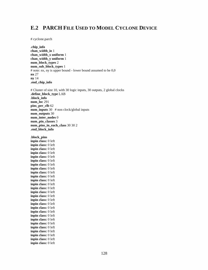
128
E.2 PARCH FILE USED TO MODEL CYCLONE DEVICE
# cyclone.parch
.chip_info
chan_width_io 1
chan_width_x uniform 1
chan_width_y uniform 1
num_block_types 2
num_sub_block_types 1
# note: nx, ny is upper bound - lower bound assumed to be 0,0
nx 27
ny 14
.end_chip_info
# Cluster of size 10, with 30 logic inputs, 30 outputs, 2 global clocks
.define_block_type LAB
.block_info
num_loc 291
pins_per_clb 62
num_inputs 30 # non clock/global inputs
num_outputs 30
num_inter_nodes 0
num_pin_classes 3
num_pins_in_each_class 30 30 2
.end_block_info
.block_pins
inpin class: 0 left
inpin class: 0 left
inpin class: 0 left
inpin class: 0 left
inpin class: 0 left
inpin class: 0 left
inpin class: 0 left
inpin class: 0 left
inpin class: 0 left
inpin class: 0 left
inpin class: 0 left
inpin class: 0 left
inpin class: 0 left
inpin class: 0 left
inpin class: 0 left
inpin class: 0 left
inpin class: 0 left
inpin class: 0 left
inpin class: 0 left
inpin class: 0 left
inpin class: 0 left
inpin class: 0 left
inpin class: 0 left
inpin class: 0 left
inpin class: 0 left
inpin class: 0 left
inpin class: 0 left
129
inpin class: 0 left
inpin class: 0 left
inpin class: 0 left
outpin class: 1 right
outpin class: 1 right
outpin class: 1 right
outpin class: 1 right
outpin class: 1 right
outpin class: 1 right
outpin class: 1 right
outpin class: 1 right
outpin class: 1 right
outpin class: 1 right
outpin class: 1 right
outpin class: 1 right
outpin class: 1 right
outpin class: 1 right
outpin class: 1 right
outpin class: 1 right
outpin class: 1 right
outpin class: 1 right
outpin class: 1 right
outpin class: 1 right
outpin class: 1 right
outpin class: 1 right
outpin class: 1 right
outpin class: 1 right
outpin class: 1 right
outpin class: 1 right
outpin class: 1 right
outpin class: 1 right
outpin class: 1 right
outpin class: 1 right
inpin class: 2 global top
inpin class: 2 global top
.end_block_pins
.block_delays
num_modes 0 # means no modes - since sub blocks will be configured with modes
# this only specified when we have no modes and the block has sub blocks
T_sblk_opin_to_sblk_ipin 335e-12
T_clb_ipin_to_sblk_ipin 0.0
T_sblk_opin_to_clb_opin 0.0
.end_block_delays
.sub_block_info
sub_blocks_per_clb 10
.end_sub_block_info
.block_loc
.max_occ 1
range 1 1 to 7 5
range 1 9 to 7 13
range 8 1 to 12 13
range 15 1 to 26 13
.end_max_occ

130
.end_block_loc
.end_define_block_type
.define_sub_block_type LCELL
.sub_block_pin_info
sub_block_inputs 12
sub_block_outputs 3
sub_block_clk_inputs 1
sub_block_inter_nodes 0
sub_block_port_names dataa datab datac datad aclr aload sclr sload ena \
cin inverta regcascin combout regout cout clk
.end_sub_block_pin_info
.sub_block_delays
num_modes 2
.mode # mode 0 - ( default )
.delay_info
delay 1 -1.0 -1.0 -1.0 -1.0 -1.0 -1.0 -1.0 -1.0 -1.0 -1.0 -1.0 -1.0 454e-12 568e-12 645e-12
delay 2 -1.0 -1.0 -1.0 -1.0 -1.0 -1.0 -1.0 -1.0 -1.0 -1.0 -1.0 -1.0 340e-12 467e-12 533e-12
delay 3 -1.0 -1.0 -1.0 -1.0 -1.0 -1.0 -1.0 -1.0 -1.0 -1.0 -1.0 -1.0 225e-12 368e-12 -1.0
delay 4 -1.0 -1.0 -1.0 -1.0 -1.0 -1.0 -1.0 -1.0 -1.0 -1.0 -1.0 -1.0 88e-12 238e-12 -1.0
delay 5 -1.0 -1.0 -1.0 -1.0 -1.0 -1.0 -1.0 -1.0 -1.0 -1.0 -1.0 -1.0 -1.0 691e-12 -1.0
delay 6 -1.0 -1.0 -1.0 -1.0 -1.0 -1.0 -1.0 -1.0 -1.0 -1.0 -1.0 -1.0 -1.0 736e-12 -1.0
delay 7 -1.0 -1.0 -1.0 -1.0 -1.0 -1.0 -1.0 -1.0 -1.0 -1.0 -1.0 -1.0 -1.0 856e-12 -1.0
delay 8 -1.0 -1.0 -1.0 -1.0 -1.0 -1.0 -1.0 -1.0 -1.0 -1.0 -1.0 -1.0 -1.0 943e-12 -1.0
delay 9 -1.0 -1.0 -1.0 -1.0 -1.0 -1.0 -1.0 -1.0 -1.0 -1.0 -1.0 -1.0 -1.0 667e-12 -1.0
delay 10 -1.0 -1.0 -1.0 -1.0 -1.0 -1.0 -1.0 -1.0 -1.0 -1.0 -1.0 -1.0 523e-12 691e-12 525e-12
delay 11 -1.0 -1.0 -1.0 -1.0 -1.0 -1.0 -1.0 -1.0 -1.0 -1.0 -1.0 -1.0 890e-12 1039e-12 525e-12
delay 12 -1.0 -1.0 -1.0 -1.0 -1.0 -1.0 -1.0 -1.0 -1.0 -1.0 -1.0 -1.0 -1.0 234e-12 -1.0
delay 13 -1.0 -1.0 -1.0 -1.0 -1.0 -1.0 -1.0 -1.0 -1.0 -1.0 -1.0 -1.0 -1.0 -1.0 -1.0
delay 14 -1.0 -1.0 -1.0 -1.0 -1.0 -1.0 -1.0 -1.0 -1.0 -1.0 -1.0 -1.0 -1.0 -1.0 -1.0
delay 15 -1.0 -1.0 -1.0 -1.0 -1.0 -1.0 -1.0 -1.0 -1.0 -1.0 -1.0 -1.0 -1.0 -1.0 -1.0
.end_delay_info
.reg_info
is_reg 0 1 0
T_setup 0.0 29e-12 0.0
T_clkToQ 0.0 173e-12 0.0
.end_reg_info
.end_mode
.mode # mode 1 - ( qfbk )
.delay_info
delay 1 -1.0 -1.0 -1.0 -1.0 -1.0 -1.0 -1.0 -1.0 -1.0 -1.0 -1.0 -1.0 454e-12 568e-12 645e-12
delay 2 -1.0 -1.0 -1.0 -1.0 -1.0 -1.0 -1.0 -1.0 -1.0 -1.0 -1.0 -1.0 340e-12 467e-12 533e-12
delay 3 -1.0 -1.0 -1.0 -1.0 -1.0 -1.0 -1.0 -1.0 -1.0 -1.0 -1.0 -1.0 225e-12 368e-12 -1.0
delay 4 -1.0 -1.0 -1.0 -1.0 -1.0 -1.0 -1.0 -1.0 -1.0 -1.0 -1.0 -1.0 88e-12 238e-12 -1.0
delay 5 -1.0 -1.0 -1.0 -1.0 -1.0 -1.0 -1.0 -1.0 -1.0 -1.0 -1.0 -1.0 -1.0 691e-12 -1.0
delay 6 -1.0 -1.0 -1.0 -1.0 -1.0 -1.0 -1.0 -1.0 -1.0 -1.0 -1.0 -1.0 -1.0 736e-12 -1.0
delay 7 -1.0 -1.0 -1.0 -1.0 -1.0 -1.0 -1.0 -1.0 -1.0 -1.0 -1.0 -1.0 -1.0 856e-12 -1.0
delay 8 -1.0 -1.0 -1.0 -1.0 -1.0 -1.0 -1.0 -1.0 -1.0 -1.0 -1.0 -1.0 -1.0 943e-12 -1.0
delay 9 -1.0 -1.0 -1.0 -1.0 -1.0 -1.0 -1.0 -1.0 -1.0 -1.0 -1.0 -1.0 -1.0 667e-12 -1.0
delay 10 -1.0 -1.0 -1.0 -1.0 -1.0 -1.0 -1.0 -1.0 -1.0 -1.0 -1.0 -1.0 523e-12 691e-12 525e-12
delay 11 -1.0 -1.0 -1.0 -1.0 -1.0 -1.0 -1.0 -1.0 -1.0 -1.0 -1.0 -1.0 890e-12 1039e-12 525e-12
delay 12 -1.0 -1.0 -1.0 -1.0 -1.0 -1.0 -1.0 -1.0 -1.0 -1.0 -1.0 -1.0 -1.0 234e-12 -1.0
delay 13 -1.0 -1.0 -1.0 -1.0 -1.0 -1.0 -1.0 -1.0 -1.0 -1.0 -1.0 -1.0 -1.0 -1.0 -1.0
delay 14 -1.0 -1.0 -1.0 -1.0 -1.0 -1.0 -1.0 -1.0 -1.0 -1.0 -1.0 -1.0 291e-12 -1.0 -1.0

131
delay 15 -1.0 -1.0 -1.0 -1.0 -1.0 -1.0 -1.0 -1.0 -1.0 -1.0 -1.0 -1.0 -1.0 -1.0 -1.0
.end_delay_info
.reg_info
is_reg 0 1 0
T_setup 0.0 29e-12 0.0
T_clkToQ 0.0 173e-12 0.0
.end_reg_info
.end_mode
.end_sub_block_delays
.end_define_sub_block_type
.define_block_type IO
.block_info
num_loc 117
pins_per_clb 13
num_inputs 8 # non clock/global inputs
num_outputs 3
num_inter_nodes 0
num_pin_classes 3
num_pins_in_each_class 8 3 2
.end_block_info
.block_pins
inpin class: 0 left
inpin class: 0 left
inpin class: 0 left
inpin class: 0 left
inpin class: 0 left
inpin class: 0 left
inpin class: 0 left
inpin class: 0 left
outpin class: 1 right
outpin class: 1 right
outpin class: 1 right
inpin class: 2 global top
inpin class: 2 global top
.end_block_pins
.block_delays
num_modes 2
.mode # mode 0 - input
.delay_info
delay 1 -1.0 -1.0 -1.0 -1.0 -1.0 -1.0 -1.0 -1.0 -1.0 -1.0 -1.0
delay 2 -1.0 -1.0 -1.0 -1.0 -1.0 -1.0 -1.0 -1.0 -1.0 -1.0 -1.0
delay 3 -1.0 -1.0 -1.0 -1.0 -1.0 -1.0 -1.0 -1.0 -1.0 -1.0 -1.0
delay 4 -1.0 -1.0 -1.0 -1.0 -1.0 -1.0 -1.0 -1.0 -1.0 -1.0 -1.0
delay 5 -1.0 -1.0 -1.0 -1.0 -1.0 -1.0 -1.0 -1.0 -1.0 181e-12 -1.0
delay 6 -1.0 -1.0 -1.0 -1.0 -1.0 -1.0 -1.0 -1.0 -1.0 -1.0 -1.0
delay 7 -1.0 -1.0 -1.0 -1.0 -1.0 -1.0 -1.0 -1.0 -1.0 -1.0 -1.0
delay 8 -1.0 -1.0 -1.0 -1.0 -1.0 -1.0 -1.0 -1.0 -1000.0 932e-12 -1.0 # 852e-12 932e-12 -1.0
delay 9 -1.0 -1.0 -1.0 -1.0 -1.0 -1.0 -1.0 -1.0 -1.0 -1.0 -1.0
delay 10 -1.0 -1.0 -1.0 -1.0 -1.0 -1.0 -1.0 -1.0 -1.0 -1.0 -1.0
delay 11 -1.0 -1.0 -1.0 -1.0 -1.0 -1.0 -1.0 -1.0 -1.0 -1.0 -1.0
.end_delay_info

132
.reg_info
is_reg 0 1 0
T_setup 0.0 598e-12 0.0
T_clkToQ 0.0 811e-12 0.0
.end_reg_info
.end_mode
.mode # mode 1 - output
.delay_info
delay 1 -1.0 -1.0 -1.0 -1.0 -1.0 -1.0 -1.0 -1000.0 -1.0 -1.0 -1.0 # 2142e-12 -1.0 -1.0 -1.0
delay 2 -1.0 -1.0 -1.0 -1.0 -1.0 -1.0 -1.0 -1.0 -1.0 -1.0 -1.0
delay 3 -1.0 -1.0 -1.0 -1.0 -1.0 -1.0 -1.0 -1.0 -1.0 -1.0 -1.0
delay 4 -1.0 -1.0 -1.0 -1.0 -1.0 -1.0 -1.0 297e-12 -1.0 -1.0 -1.0
delay 5 -1.0 -1.0 -1.0 -1.0 -1.0 -1.0 -1.0 -1.0 -1.0 -1.0 -1.0
delay 6 -1.0 -1.0 -1.0 -1.0 -1.0 -1.0 -1.0 -1.0 -1.0 -1.0 -1.0
delay 7 -1.0 -1.0 -1.0 -1.0 -1.0 -1.0 -1.0 -1.0 -1.0 -1.0 -1.0
delay 8 -1.0 -1.0 -1.0 -1.0 -1.0 -1.0 -1.0 -1.0 -1.0 -1.0 -1.0
delay 9 -1.0 -1.0 -1.0 -1.0 -1.0 -1.0 -1.0 -1.0 -1.0 -1.0 -1.0
delay 10 -1.0 -1.0 -1.0 -1.0 -1.0 -1.0 -1.0 -1.0 -1.0 -1.0 -1.0
delay 11 -1.0 -1.0 -1.0 -1.0 -1.0 -1.0 -1.0 -1.0 -1.0 -1.0 -1.0
.end_delay_info
.reg_info
is_reg 0 1 0
T_setup 0.0 598e-12 0.0
T_clkToQ 0.0 811e-12 0.0
.end_reg_info
.end_mode
.end_block_delays
.sub_block_info
sub_blocks_per_clb 0
.end_sub_block_info
.block_loc
.max_occ 2
line x 0 y 1 2 3 4 5 9 10 11 12 13
line x 27 y 1 2 3 4 5 9 10 11 12 13
line y 0 x 2 4 6 10 18 22 24 26
line y 14 x 2 4 6 10 18 22 24 26
.end_max_occ
.max_occ 3
line x 0 y 6 7 8
line x 27 y 6 7
line y 0 x 8 12 16 20
line y 14 x 8 12 16 20
.end_max_occ
.max_occ 6
line x 27 y 8
.end_max_occ
.end_block_loc
.end_define_block_type

133
F TOOL SETTINGS
F.1 DC SETTINGS
The DC tool is setup by default to focus more on improving the timing of a circuit than
on deceasing the amount of wire used.
F.2 DP SETTINGS
The DP tool is setup by default to focus on improving the timing of a circuit and
deceasing the amount of wire used. The default value that is set produces the best timing
results.
F.3 QUARTUS II SETTINGS
The following settings in Quartus II was included to force Quartus II tools to focus on
improving the timing of the circuit and provide a fair comparison between Quartus II
CAD software and the DC and DP tools.
set_global_assignment -name STRATIX_OPTIMIZATION_TECHNIQUE SPEED
set_global_assignment -name FMAX_REQUIREMENT "1000.0 MHz"
set_global_assignment -name IGNORE_CLOCK_SETTINGS ON
set_global_assignment -name FINAL_PLACEMENT_OPTIMIZATION NEVER
set_global_assignment -name AUTO_PACKED_REGISTERS_STRATIX OFF
set_global_assignment -name ERROR_CHECK_FREQUENCY_DIVISOR 1