abstracts brochure 2014 - Loughborough University · vacuum deposition integrated with design of...
20
Innovative electronics Manufacturing Research Centre www.iemrc.org IeMRC Innovative electronics Manufacturing Research Centre Research Portfolio 2010-2015
Transcript of abstracts brochure 2014 - Loughborough University · vacuum deposition integrated with design of...

Innovative electronics Manufacturing Research Centrewww.iemrc.org
IeMRC
Innovative electronics Manufacturing Research Centre
Research Portfolio 2010-2015

Project title Institutes (FEC) Value
Flagship: Roll to roll Vacuum processed Carbon Based Electronics OxfordManchesterBangorLeeds
£1,377,326
Flagship: Smart microsystems EdinburghHeriot-Watt
£1,470,834
High performance fl exible, fabric electronics for MHz frequency communications LoughboroughNottingham Trent
£465,249
Costing for avionic through life availability BathLoughboroughUWE
£513,568
WHISKERMIT: Manufacturing & in-service tin whisker mitigation strategies for high value electronics
Loughborough £404,900
High performance low-cost power modules for energy smart network applications Nottingham £442,347
Sustainable ultrasonic electroless & immersion plating processes for photovoltaic & PCB manufacture
Coventry £339,942
3-D Microwave & mm-wave system-on-substrate using sacrifi cial layers for printed MEMS components
LeedsImperial College LondonLoughborough
£377,483
Design for increased yield for the electronics manufacturing supply chain Loughborough £263,286
Thermosonic-adhesive fl ip chip assembly for advanced microelectronic packaging Imperial College London £210,674
Micro-interconnects using mono-sized polymer microspheres for large format high resolution sensor packaging
Loughborough £167,833
Electrochemically assisted integration of organic semiconductors on CMOS & MEMS Strathclyde £107,843
Sustaining Electronic Industry through managing uncertaintanty in contract bidding BathLoughborough
£149,650
Robustness design & health management in power electronics using damage me-chanics based models
NottinghamGreenwich
£528,474
Conductive resists for nanofabrication on insulating substrates Birmingham £344,401
Carbon nanotube composite surfaces for electrical contact interfaces Southampton £489,345
Functionalisation of copper nanoparticles to enable metallisation in electronics manu-facturing
CoventryLoughborough
£383,662
Innovative electronics Manufacturing Research Centrewww.iemrc.org
IeMRC
Project portfolio

Innovative electronics Manufacturing Research Centrewww.iemrc.org
About the Centre
The IeMRC was established in 2004 to provide the UK’s electronics manufacturing sector with access to world-class academic research. With an initial £5.5million support for 5 years from the Engineering and Physical Science Research Council, the Centre secured a further £10million (FEC) up to 2015 following an international review. Since 2010 the Centre has commissioned new research projects to continue delivering to its vision:
The Centre has a virtual hub located at Loughborough University, with Academic Executive support from Bath, Brunel, Greenwich, Heriot-Watt, Lancaster and Nottingham universities. The Centre’s re-search priorities are guided by an Industrial Steering Group that has representation from the entire electronics manufacturing supply chain.
The Centre Since 2010, 17 Universities across the UK have been allocated funding to conduct research worth £8million. These projects have attracted industrial support from 81 separate businesses with a combined in-kind and direct contribution value of £4.4million. To optimise the potential for innovation each project often has full industrial supply chain input.
The following pages provide an insight to the research activity supported by the Centre and highlights the diverse electronics manufacturing activity within the UK.
In addition to funding research, the Centre supports the UK’s electronics manufacturing sector with quaterly seminars and its fl agship event, its Annual Conference. The events provide ideal opportunities to form new collaborations and promote academic and industrial interaction.
For further information on the Centre, its activities and research projects, then please visit our website www.iemrc.org or follow us on twitter @iemrc
The vision of the IeMRC is to be the UK’s internationally recognised provider of world-class electronics manufacturing research. It will
focus on sustaining and growing high value manufacturing in the UK by delivering innovative and exploitable new technologies through
its highly skilled people and by providing strategic value to the electronics industry.
IeMRC

IeMRC
IeMRC Flagship Project
Roll-to-roll Vacuum Processed Carbon Based
Electronics (RoVaCBE)
Primary Investigator:
Hazel Assender, University of Oxford
Partner Institutes:
Universities of Leeds,
Manchester & Bangor
Electronics components that can be manufac-tured using roll-to-roll processing off er the possibil-ity of lower cost devices as well as those that might be mechanically fl exible in use. Roll-to-roll (R2R) processing, using a fl exible substrate (typically a polymer fi lm) allows for cheap production of many components very rapidly, with low energy require-ments. Key areas of exploitation of this technology include fl exible displays, but there is also a wealth of lower-cost applications. Tagging and tracking of fast moving consumer goods is an example technol-ogy that truly exploit the very low-cost nature of the production and in which the manufacturing is closely linked to the manufacturing routes currently exploited for e.g. packaging technologies. Carbon based electronics (CBE) based on polymer and/or organic molecular materials has been identifi ed and a high priority development area, and much inter-est in research to date has focussed around solvent-based processing. This proposal seeks to exploit the existing industrialised technology of vacuum R2R processing, widely used for example in the packaging industry, to develop the manufacture of very low cost organic fi eld-eff ect transistor (OFET)-based devices and circuits. This manufacturing route, like solvent
based systems, is cheap and provides fl exible product, and we can exploit high electrical mobility molecular semiconductors. Additional advantages of the solvent-free vacuum processes include: a) likely enhanced web-speed, b) integration with vacuum-based metal deposition for conducting channels, and metal or ceramic deposition for barrier layers and possible interfacial modifi cation, and c) the ability to deposit multiple thin layers to build up device struc-tures without solvent interactions with underlying layers. The project will exploit our existing R2R web processing facility to explore the principal manufac-turing challenges to R2R vacuum production of OFET devices: 1) selection and adaptation of materials to vacuum deposition integrated with design of suit-able circuitry, 2) patterning of the semiconductor and insulator layers to allow the formation of circuit connections between devices and 3) reliability of manufacture to be able to produce arrays of multiple transistors for circuits. It will allow us to explore and develop the deposition of molecular semiconductor and dielectric materials and then the subsequent reliability and thermo-mechanical resilience of the re-sulting product such that it might need to withstand, for example, during a lamination process.
Innovative electronics Manufacturing Research Centre
www.iemrc.org

IeMRC
IeMRC Flagship Project
SMART Microsystems
Primary Investigator:
Anthony Walton, University of Edinburgh
Partner Institute:
Heriot Watt University
The Smart Microsystems concept promises to ex-tend the functionality of standard Integrated Circuit (IC) technology by combining it with a wide variety of diff erent materials, sensors and actuators.
The integration of novel Microsystems technologies with the processing power of modern silicon elec-tronics has the potential to transform a wide variety of application areas ranging from medical diagnostics and sensing to consumer electronics.
Post processing of CMOS (the standard technology for silicon electronics) involves the addition of new structures and materials on top of ICs to add value and extend functionality.
Although the UK is very strong in the fi eld of IC de-sign most of the advanced CMOS fabrication is now performed in silicon foundries in the Far East. How-ever, the move to foundries means that the ICs have become a commodity where the added value can come from bespoke post-processed technologies.
The Smart Microsystems group is made up from members of the Institute of Integrated Systems which brings together researchers from the Universi-ties of Edinburgh and Heriot who have many years of experience in the development of microsystems technologies, some of which have led to very suc-cessful spin-out companies.
The IIS is one of the few research groupings in the UK with the capability to bring together IC design-ers, materials specialists and process technologists in one place to develop exciting and novel technologies for integrated microsystems with great potential for knowledge transfer and commercial exploitation.
They will work with a number of industrial partners, led by National Semiconductor, to develop new materials, production methods, and post processed microsystems, with the aim of generating knowledge that will greatly benefi t the UK economy.
Innovative electronics Manufacturing Research Centre
www.iemrc.org
IeMRC Flagship Project
SMART Microsystems
Primary Investigator:
Anthony Walton, Universittyyyyyyyy ooofff Eddiinnnbbbbuuuuurrgggghhhhhhhhhhh
Partner Institute:
Heriot Watt Univveeeeeeerrrrrrrssiiiiity

IeMRC
IeMRC Standard Project
Thermosonic-adhesive fl ip chip assembly for
advanced microelectronic packaging
Primary Investigator:
Andrew Holmes, Imperial College London
This project aims to improve the performance and reliability of fl ip chip assembly methods based on anisotropic conductive and non-conductive adhe-sives (ACAs and NCAs).
Flip chip assembly is a technique used in advanced electronics manufacturing. It allows unpackaged in-tegrated circuits or “chips” to be attached to a circuit board or other substrate in a face-down confi gura-tion, with electrical connections between the contact pads on the chip and the substrate being provided by conducting “bumps”.
Flip chip assembly off ers numerous advantages over other chip attachment methods, including higher electrical performance, higher interconnect density (more electrical connections per unit area), smaller footprint and lower height.
In ACA and NCA fl ip chip processes, the chip is bond-ed to the substrate by a layer of adhesive which is deposited on the substrate before the chip is placed in position.
The diff erence between the two approaches is that NCA fl ip chip relies on direct metal-metal contact between the chip bump and substrate pad, while in ACA fl ip chip this connection is mediated by small conductive particles dispersed in the adhesive.
Both ACA and NCA processes off er advantages over more traditional methods based on solder bonding, including scalability to higher interconnect densities, lower process complexity, and lower temperature processing.
However, they rely on purely mechanical contacts for electrical connectivity, and these tend to have higher resistance and lower reliability than solder joints. As a result, ACA and NCA technologies are considerably less pervasive than they should be, and are found in only a relatively small number of applica-tions.
The aim of the proposed research is to introduce thermosonic bonding into ACA and NCA fl ip chip processes in order to replace the mechanical contacts by metal-metal bonds.
The project is expected to deliver processes that retain all the advantages of existing ACA/NCA technology, while at the same time off ering higher performance and reliability. Like existing ACA/NCA processes, the new processes will be lead-free and will avoid metal-eutectic bonding. They will therefore have a positive environmental impact in any applica-tion where they can replace solder-based fl ip-chipassembly.
If successful, the research will lead to a next genera-tion fl ip chip technology with wide ranging appli-cations. This will enhance the UK’s already strong position as a centre for innovation in electronics man-ufacturing, and also provide a valuable new technol-ogy for the electronics manufacturing industry.
Innovative electronics Manufacturing Research Centre
www.iemrc.org
IeMRC
IeMRC Standard Project
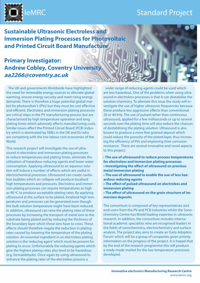
Sustainable Ultrasonic Electroless and
Immersion Plating Processes for Photovoltaic
and Printed Circuit Board Manufacture
Primary Investigator:
Andrew Cobley, Coventry University
The UK and governments Worldwide have highlighted the need for renewable energy sources to alleviate global warming, ensure energy security and meet rising energy demands. There is therefore a huge potential global mar-ket for photovoltaic’s (PVs) but they must be cost eff ective and effi cient. Electroless and immersion plating processes are critical steps in the PV manufacturing process but are characterised by high temperature operation and long plating times which adversely aff ects manufacturing costs. Similar issues aff ect the Printed Circuit Board (PCB) indus-try which is dominated by SMEs in the UK and EU who are competing with the low labour cost economies of the World.
This research project will investigate the use of ultra-sound in electroless and immersion plating processes to reduce temperatures and plating times, eliminate the utilization of hazardous reducing agents and lower water consumption. Applying ultrasound to an aqueous solu-tion will induce a number of eff ects which are useful in electrochemical processes. Ultrasound can create cavita-tion bubbles which on collapse will produce localised high temperatures and pressures. Electroless and immer-sion plating processes can require temperatures as high as 90 ºC to produce acceptable plating rates. By applying ultrasound at the surface to be plated, localised high tem-peratures and pressures can be generated even though the bulk solution temperature might have been reduced. In addition, ultrasound can raise the plating rates of these processes by increasing the transport of metal ions to the substrate being plated and by reducing the thickness of the boundary layer which these ions have to cross. These eff ects should therefore negate the reduction in plating rates caused by lowering the temperature of the plating solution. An essential ingredient in an electroless plating solution is the ‘reducing agent’ which must be present for plating to occur. Unfortunately the reducing agents which give the highest plating rates also tend to be hazardous (e.g. formaldehyde). Once again by using ultrasound to enhance the plating rates of the electroless process a
wider range of reducing agents could be used which are less hazardous. One of the problems when using ultra-sound in electroless processes is that it can destabilize the solution chemistry. To alleviate this issue the study will in-vestigate the use of higher ultrasonic frequencies because these produce less aggressive eff ects than conventional 20 or 40 kHz. The use of pulsed rather than continuous ultrasound, applied for a few milliseconds or up to several seconds over the plating time will also reduce the chances of destabilising the plating solution. Ultrasound is also known to produce a more fi ne grained deposit which could reduce the porosity of the plated layer, thus increas-ing the effi ciency of PVs and improving their corrosion resistance. There are several innovative and novel aspects to this project;
• The use of ultrasound to reduce process temperatures
for electroless and immersion plating processes
• Investigating the eff ect of ultrasound on precious
metal immersion plating
• The use of ultrasound to enable the use of less haz-
ardous reducing agents
• The eff ect of pulsed ultrasound on electroless and
immersion plating
• The eff ect of ultrasound on the grain structure of im-
mersion deposits
The consortium is composed of key representatives and end-users from the PV and PCB industries whilst the Sono-chemistry Centre has World leading expertise in ultrasonic research. In addition, the consortium includes interna-tional academic specialists who are recognised leaders in the fi elds of sonochemistry, electrochemistry and surface analysis. The project also aims to create an ‘Early Adopters Forum’ which will be a group of companies given priority information on the progress of the project. It is hoped that by the end of the research programme this will produce a ready-made market for the low temperature processes developed.
Innovative electronics Manufacturing Research Centre
www.iemrc.org

Abstracts
IeMRC
Innovative electronics Manufacturing Research Centrewww.iemrc.org
Projects
High-performance low-cost power modules for energy smart network
applications
Mark Johnson, University of Nottingham. [email protected]
According to the UK Government’s Low Carbon Transition Plan, by 2030 we will see a step change in intermittent generation delivered through both large and small scale renewable plants, more price responsive consumers enabled by smart meters and possible increases in demand for electricity from changes in power use, such as a move to electric vehicles. The electricity grid will to need to evolve in order to connect and integrate new technologies and enable more active management of fl uctua-tions in supply and demand. Smart grids or networks, consisting of a collection of energy producers (generators), energy consumers, energy storage devices and power fl ow control elements combined with intelligent controls that adjust the operation and confi guration of the network will be needed to ensure security of supply, optimal use of available energy resource and maximum effi ciency. Power electronic systems enabled by the power modules that are the subject of this proposal will lie at the heart of the control elements of these smart networks. The known requirements for IGBT modules in electricity network applications include high isolation voltage (>10 kV), excellent cooling performance, high reliability and a preference for fail-to-short-circuit behaviour in the event of device destruction. Present state-of-the-art manufacturing for plastic packaged IGBT modules involves the solder attachment of the dies to a substrate followed by ultra-sonic bonding of IGBT emitter and diode anode connections, there being up to 600 individual bonds in a large module. Creation of such a large number of individual bonds is expensive, time consuming and a source of yield loss. During operation, the wires are a known reliability weak point and in the event of device destruction the bond wires typically fail open-circuit by a high energy fusing process. This failure process is inherently unpredictable and the high energies dissipated within the module can lead to rupture of the module housing. In addition, the typical bond wire and bus-bar assembly leads to relatively high levels of parasitic inductance which compromises device switching perfor-mance leading to increased switching loss and/or over-rating of device blocking voltage. Finally, the thermal management arrangements in conventional modules take heat away from just one die sur-face, restricting the maximum heat fl ux that can be sustained for a given maximum junction tempera-ture. Planar or “sandwich” packages have no bond wires, can be cooled from both sides and can off er fail-to-short-circuit operation. Although potentially attractive, the assembly of such structures has histori-cally proved complex and costly, involving a large number of piece parts and assembly processes. This project will deliver technologies to reduce the manufacturing costs and improve the performance of plastic packaged IGBT modules. Research into a high thermal performance low profi le package, de-signed for low inductance and having fully bonded interconnects will deliver step improvements in performance/reliability and reduced manufacturing cost. An important characteristic of the package will be its capability to fail to short circuit, a unique feature which is highly benefi cial in reducing elec-tricity network system costs but is not currently available in plastic packaged IGBT modules.

Abstracts
IeMRC
Innovative electronics Manufacturing Research Centrewww.iemrc.org
Projects
The power electronic controls that form the application target of this research are excellent examples of high value systems that must be customised to meet individual customers’ requirements. There is thus substantial potential for growth in the global market and the UK is in an excellent position to capitalise on this growth. Our long-term aspiration is that the step changes in technology described in this proposal will increase the competitiveness of UK power module manufacturing and enable UK system providers to rise to the challenges and opportunities presented by smart networks.
Micro-interconnects Using Mono-sized Polymer Microspheres for Large Format High Resolution
Sensor Packaging
Changqing Liu, Loughborough University. [email protected]
Challenges and bottlenecks remain in the endeavour to deliver ultra-fi ne pitch interconnects for μBGA and fl ip-chip devices. There are two major factors that are of particular concern in the acquisition of such future generation technologies: i) the complexity associated with the micro-scale deposition of materials, and ii) the achievement of acceptable yields. As for the assembly equipment, alignment and bonding processes will become extremely critical. While the demands on reducing the gap between silicon foundry and wafer level packaging have so far been delivered, through various concepts in-cluding System in Package and System on Package, the search continues for assembly processes that are capable of interconnects at a pitch close to 10 microns to meet current and future demands of highly functional semiconductor devices. This project is to carry out a feasibility study to enable such fi ner pitch interconnects through the use of novel materials and processes. The proposed work will use monosized metal coated polymer based micro-spheres specially fabricated by Conpart, a Nor-wegian company, to achieve ultrafi ne pitch interconnects by replacing traditional solder joints. Due to the unique polymerisation process used to fabricate the particles, their size and the chemical and mechanical properties can be tailored, with extreme accuracy and reproducibility. This, combined with metal plating technology, makes these spheres ideal as conductive elements which have been widely used in the anisotropic conductive adhesives (ACAs) used in fl at panel display assembly. The extension of this technology to the direct replacement of solid solder balls in μBGA and fl ip-chip assembly is cur-rently of great interest for increasing the compliancy of the interconnections as a route to improved product reliability under thermal fatigues and shock loading. This feasibility study will explore the possibility of creating interconnections with such mono-sized polymer spheres for applications which demand connection pitches as fi ne as 10 microns, such as in X-ray detectors.

Abstracts
IeMRC
Innovative electronics Manufacturing Research Centrewww.iemrc.org
Projects
Costing for avionic through life availability (CATA)
Linda Newnes, Bath University. [email protected]
Partner Institutes: University of the West of England, Loughborough University.
This research programme aims to provide novel approaches to predict the manufacture and repair costs through life for in-service avionic systems. To achieve this aim the collaboration includes three UK academic institutions, three industrial collaborators and two international research groups. These have been selected to provide expertise in the supply chain, through life costing, assessing uncertain-ty and to represent the supply chain from concept design through to manufacture and disposal. The outcomes from the research will be a set of modelling tools and processes which have been validated by the industrial partners. To model the in-service manufacturing and repair costs through life will en-able a step change in the UKs capability to get value for money and manage through life costs.
3D Microwave & Millimetre-Wave System-on-Substrate using Sacrifi cial Layers for Printed RF
MEMS Components
Ian Robertson, University of Leeds. [email protected]
Partner Institutes: Imperial College London, Loughborough University.
Microwave and millimetre-wave systems are used extensively in communications, radar, imaging and sensing applications. System-on-substrate (SoS) technology is an exciting new concept where bulky coaxial cables and rectangular waveguide interconnects are replaced by low loss transmission lines embedded into a multilayer substrate that incorporates a wide range of components and subsystems. The advantages of this approach are dramatically enhanced if Radiofrequency (RF) Microelectrome-chanical Systems (MEMS) can be integrated into the substrate. MEMS components have had an explo-sive impact on consumer products including the iPhone and Nintendo Wii motion-sensing devices. Currently these products are fabricated with expensive silicon technology. From a manufacturing cost perspective, it is a much more attractive proposition to be able to fabricate the RF MEMS components in ceramic or organic laminate technology – i.e. directly onto a printed circuit board. This would lead to a technology capable of being used to manufacture large-scale system-on-substrate designs for applications such as scanning antenna arrays and adaptive stealth materials for a range of applica-tions at microwave and millimetre-wave frequencies. It is proposed that these novel embedded RF MEMS components can be fabricated by employing screen printing and by developing novel techniquesbased on sacrifi cial layers which are removed in acontrolled manner during fi ring. It is envisaged that
Abstracts
IeMRC
Innovative electronics Manufacturing Research Centrewww.iemrc.org
Projects
an eff ective and manufacturable solution would have a signifi cant impact on UK industry in the area.
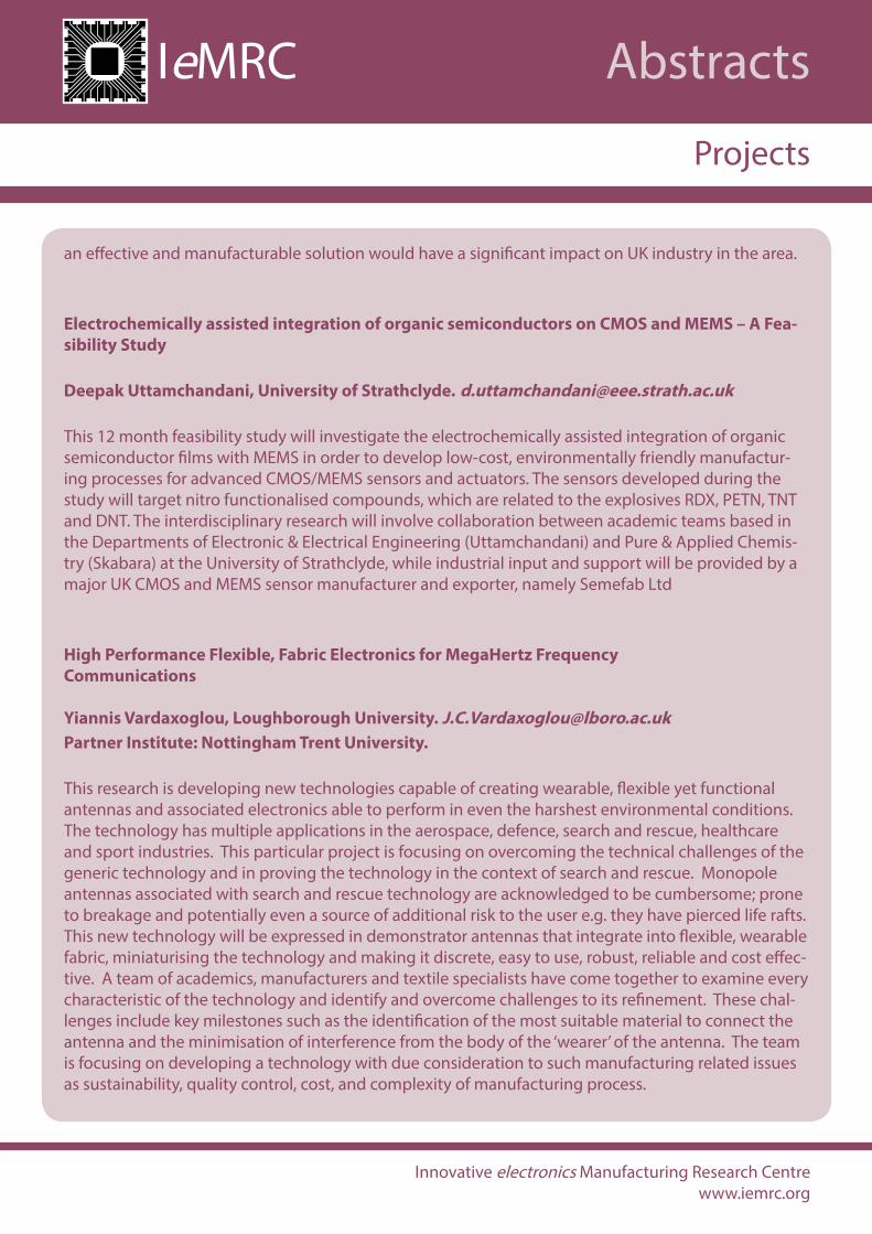
Electrochemically assisted integration of organic semiconductors on CMOS and MEMS – A Fea-
sibility Study
Deepak Uttamchandani, University of Strathclyde. [email protected]
This 12 month feasibility study will investigate the electrochemically assisted integration of organic semiconductor fi lms with MEMS in order to develop low-cost, environmentally friendly manufactur-ing processes for advanced CMOS/MEMS sensors and actuators. The sensors developed during the study will target nitro functionalised compounds, which are related to the explosives RDX, PETN, TNT and DNT. The interdisciplinary research will involve collaboration between academic teams based in the Departments of Electronic & Electrical Engineering (Uttamchandani) and Pure & Applied Chemis-try (Skabara) at the University of Strathclyde, while industrial input and support will be provided by a major UK CMOS and MEMS sensor manufacturer and exporter, namely Semefab Ltd
High Performance Flexible, Fabric Electronics for MegaHertz Frequency
Communications
Yiannis Vardaxoglou, Loughborough University. [email protected]
Partner Institute: Nottingham Trent University.
This research is developing new technologies capable of creating wearable, fl exible yet functional antennas and associated electronics able to perform in even the harshest environmental conditions. The technology has multiple applications in the aerospace, defence, search and rescue, healthcare and sport industries. This particular project is focusing on overcoming the technical challenges of the generic technology and in proving the technology in the context of search and rescue. Monopole antennas associated with search and rescue technology are acknowledged to be cumbersome; prone to breakage and potentially even a source of additional risk to the user e.g. they have pierced life rafts. This new technology will be expressed in demonstrator antennas that integrate into fl exible, wearable fabric, miniaturising the technology and making it discrete, easy to use, robust, reliable and cost eff ec-tive. A team of academics, manufacturers and textile specialists have come together to examine every characteristic of the technology and identify and overcome challenges to its refi nement. These chal-lenges include key milestones such as the identifi cation of the most suitable material to connect the antenna and the minimisation of interference from the body of the ‘wearer’ of the antenna. The team is focusing on developing a technology with due consideration to such manufacturing related issues as sustainability, quality control, cost, and complexity of manufacturing process.

Abstracts
IeMRC
Innovative electronics Manufacturing Research Centrewww.iemrc.org
Projects
The project will deliver research and technology infrastructure that has been rigorously tested and designed not only to meet the needs of the end-user but also to be capable of being manufactured by a process which meets the criteria of best practice in the industry ; sustainable, cost-eff ective, and of the highest quality. The technology has the potential to spread to a number of industry sectors and these opportunities are also being explored and defi ned. New markets might include antennas in clothing for vulnerable people such as dementia patients and young children. The device could also be integrated into the packaging of emergency aid drops to assist people on the ground to locate emergency supplies or adapted further to integrate into remote patient monitoring devices to enable patients to remain at home.
The research’s primary goal is to research and test the capability of the technology through the de-sign of a fabric-based antenna capable of maintaining a strong radio signal, even when the antenna is slightly bent vertically, horizontally or diagonally and send location information to a remote control centre. This demonstrator will also be subject to challenging environmental testing to ascertain the limits of the technology’s performance. The objectives of this project will be achieved by a team ap-proach, ensuring that the expertise and industry insight of each partner is fully utilised. An initial step will be to fully understand the capabilities of the antenna using computer simulations. A wide-range of testing scenarios will be simulated and investigated. These will include extremes of temperature, precipitation and salination. The results will be used to inform the development of representative samples that can be further tested and measured. This detailed process will feed into the pre-produc-tion prototyping drawing on the expertise of our industrial partners in manufacturing and the aca-demic specialists in textile fabrication at Nottingham Trent University. Laboratory and pre-production prototypes will be repeatedly tested and refi ned until optimum capability is reached.

Abstracts
IeMRC
Innovative electronics Manufacturing Research Centrewww.iemrc.org
Projects
Design for Increased Yield for the Electronics Manufacturing Supply Chain (DIY)
Andrew West, Loughborough University. [email protected]
The aim of the DIY project is to provide an integrated software Design for X toolkit for aerospace elec-tronics manufacturing products applicable throughout the:
1. electronics manufacturing supply chain (i.e. bare board manufacture, assembly, end user applications) 2. electronics product and process lifecycle (i.e. design, specifi cation, analysis, manufacture, test, deploy, maintain, reuse)
The toolkit will be based upon a number of integrated sources of knowledge. Partner design, manu-facturing and operational rules will be sourced along with the determination of a suite of reduced order “physics of failure” models of the key electronics manufacturing processes. Data centric models will be derived from design and analysis of appropriate test vehicles and experiments encapsulating relevant design features, components, materials and processes as identifi ed by the supply chain part-ners. Integration of these models will enhance the capability of the toolkit and support the not only the prediction of sources of quality and reliability issues but also a root cause analysis capability.
WHISKERMIT: Manufacturing and in-service tin whisker mitigation strategies for high value
electronics
Geoff Wilcox, Loughborough University. [email protected]
Tin (Sn)-based metal coatings, such as those produced by electroplating, are widely used in electronics manufacture as solderable surfaces and as general protection to guard against corrosion and oxida-tion of underlying metal surfaces. Tin (along with zinc and cadmium) can produce hair-like growths often exceeding 5 mm in length. The propensity for these growths to cause inherent shorting failures in electronics, particularly with very small inter-component spacings, is very marked. In the past the capacity of electroplated tin coatings to produce tin whiskers was signifi cantly reduced by the alloying of tin with in excess of 3% lead (Pb). Recent environmental laws banning the use of lead in electronics has removed this safeguard. Consequently, the occurrence and threat posed by tin whiskers has risen to worrying levels, particularly where manufacturers have used bright tin fi nishes which are renown for tin whisker formation.
The WHISKERMIT project will examine tin whisker mitigation through a dual approach. Firstly the pro-ject will characterise a commercial bright tin electroplating electrolyte to use as a baseline onto which modifi cations in terms of compressive stress-relieving additions can be made. These additions will be

IeMRC
Innovative electronics Manufacturing Research Centrewww.iemrc.org
in the form of co-deposited nano-particulates which have been shown to reduce internal stresses in other composite electroplating systems. Accelerated whisker testing will be undertaken using in-house and industrial partner facilities to measure whisker reduction. The second phase of the project will formulate a new whisker mitigating polymeric coating through structural and compositional modifi cation. This will be achieved by examining how whiskers interact with known polymer fi lms and which chemical formats and physical properties produce true reductions in whisker emergence through such fi lms. Data from these trials will be utilised to produce novel nanostructured polymer coatings (NNPCs) with inherent properties to stem tin whisker growth. Their effi cacy in terms of tin whisker mitigation will be examined via accelerated environmental testing. The duality of a combined modifi ed tin electroplating system and a NNPC will also be assessed.
Sustaining Electronic Industry through managing uncertaintanty in contract bidding
Linda Newnes, University of Bath. [email protected]
Partner Institute: Loughborough University.
This research focuses on electronics manufacturing companies of large infrastructure, high-value elec-tronic systems who are facing the challenge of changing market structures. They are more and more required to provide services and product service systems as opposed to off ering products. This devel-opment has also been described as servitisation. This leaves them with a high level of uncertainty due to the novelty of the process and the long-term nature of services. This uncertainty is intensifi ed by global competition and the pressure for high productivity to secure competitive advantage.The aim of this project is to provide the electronic product-service integrators with a tool to assist in the decision of contract pricing to win future design, manufacture and operations & support contracts for large infrastructure, high-value electronic systems. It will defi ne a process for the facilitation of this support in the form of a decision matrix which includes the probability of winning the contract, the probability of making a profi t and the expected value of this profi t. The process includes the identifi ca-tion of the inherent uncertainty in a pricing decision to the design of a decision matrix representing the modelling outcome of this uncertainty.
Robustness design & health management in power electronics using damage mechanics based
models
Mark Johnson, University of Nottingham. [email protected]
Partner Institute: University of Greenwich.
Power electronics is a £70bn direct global market, growing at a rate of 11.7% per annum. It is essential to all future sustainable energy scenarios and is thus a critical technology for a large proportion of UK
Abstracts
Projects

IeMRC
Abstracts
industry. Despite this importance, there is increasing evidence that many power electronic devices and systems are unsuited to the stringent demands of energy and transport applications, for example off shore wind and electric vehicles, where unpredictable, fl uctuating loads and exposure to widely varying environmental conditions present a particularly challenging environment. Reliability design methods applied to power electronic modules are currently unable to capture the complex nature of such loads and additionally, do not account for the microstructural evolution of bonding and intercon-nect materials during degradation, which further restricts their application. Resulting designs thus tend to be conservative, leading to high capital costs and low confi dence in predictions of in-service life. The aim of this project is to extend physics-of-failure-based wear-out models, and associated robustness design and health management methodologies to meet the requirements of power elec-tronics in future transport and energy systems.
Work will commence with the development of damage mechanics based models for key bonding and interconnect technologies that include the eff ects of microstructural changes, for example due to thermal exposure. These new damage models will be incorporated into time-domain physics-of-failure models which can accurately refl ect the infl uence of arbitrary loading. A risk-based approach to reliability prediction will be adopted which can take account of uncertainties in the manufacturing processes including material properties, geometry, etc. Finally our fusion-based prognostics approach for power electronic assemblies will be enhanced to include the latest physics of failure models, hence to monitor power module material degradation and remaining useful life, both during qualifi cation testing and in the fi eld.
Conductive resists for nanofabrication on insulating substrates
Alex Robinson, University of Birmingham. [email protected]
Electron Beam Lithography (EBL) is particularly well suited to high value/low volume nanodevice manufacture. However, for glass and GaN, which are very poor conductors, the use of EBL leads to problems as the electrons in the beam cause the substrate to charge up, which then starts to defl ect the electron beam unpredictably leading to distortion of the lithography pattern. It has not yet been possible to fabricate sub-100 nm structures on either GaN or glass using standard EBL techniques. It would be highly advantageous to break the 100 nm barrier as this would lead to signifi cant device improvements
This project will create a new high speed and resolution electron beam resist that is also conductive. This will allow the beam electrons to discharge harmless to ground and thus prevent charging related pattern distortion. Such a resist will enable signifi cant advances in electroforming on glass and GaN manufacturing capabilities. Additional benefi ts of such a resist would be seen in a wide range of other insulating substrate patterning applications such as II-VI, diamond electronics and plastic nanopat-terning.
Innovative electronics Manufacturing Research Centrewww.iemrc.org
Projects

Abstracts
IeMRC
Innovative electronics Manufacturing Research Centrewww.iemrc.org
Projects
Carbon nanotube composite surfaces for electrical contact interfaces
John McBride, University of Southampton. [email protected]
Electrical contacts are often the weakest link in electrical and electronic systems. As engineering sys-tems become increasingly complex, with ever increasing numbers of embedded electronics, sensors and actuators; this issue will become more important. As the demand for reliable electrical contacts increases, the opportunity also grows for introducing innovative solutions using emerging material systems combined with innovative design approaches stemming from a fundamental understanding of the mechanisms determining contact performance. The research is focused on low current electro-mechanical (EM) switching devices, which are core to a vast array of systems. The key advantages of EM devices over solid state devices are; electrical isolation, lower losses, smaller volume, lower cost and higher current handling capability per unit volume; this project is focused on MEMS (Micro-Elec-tro-Mechanical Systems) relay devices; where the requirement is for lifetimes >108 switching cycles, with minimal interface wear or degradation, is particularly demanding. A solution to this problem has the potential to have a profound impact on a range of electrical and electronic applications, for exam-ple in consumer electronics as power control devices to extend battery life, or in RF MEMS switching. The research will investigate the new composite surfaces; consisting of a layer of multi-walled, verti-cally aligned carbon-nanotubes, coated with a conductive gold layer. The study will include a full in-vestigation of the physical properties of these surfaces. The understanding of the contact, and impact mechanics; the conduction mechanisms, both thermal and electrical; will allow the optimisation of the surfaces. The optimisation will also allow manufacturing processes to be established, and applied in the manufacturing of MEMS switching devices.
Functionalisation of copper nanoparticles to enable metallisation in electronics manufacturing
Andy Cobley, Coventry University. [email protected]
Partner Institute: Loughborough University.
The UK electronics industry is dominated by SMEs and the manufacturing processes they use must become cost eff ective and effi cient if they are to compete with the low cost economies of the World. An underpinning technology within the electronics industry is the requirement to metallise dielectric materials to form conductive tracks and vias for interconnection on a range of materials such as PCBs, RFID tags and plastics. One of the most common methods of metallisation is electroless plating which utilizes precious metals principally for their catalytic properties but these are problematic in terms of expense, scarcity and resource effi ciency. The R&D costs associated with developing new metallisation processes are signifi cant and the large corporate suppliers are reluctant to invest in developing ‘pre-cious metal free’ metallisation processes. There is therefore a gap between what is required by SMEs and what is provided by their suppliers. This research programme will fi ll this gap by producing low cost metallisation processes which are applicable to high value electronic manufacturing sectors.

Abstracts
IeMRC
Innovative electronics Manufacturing Research Centrewww.iemrc.org
Projects
This project will take commercially produced copper nanoparticles (CuNP) and attach molecules to them which will change their surface properties. This is a process known as functionalisation. To ensure that the CuNP are completely covered by these molecules, and to prevent agglomeration, ultrasound will be used as a dispersive technique. This functionalisation will enable them to attach to a range of substrates to act as a catalytic seed layer for electroless metallisation. In this respect, the CuNP can be seen as a replacement for palladium. To further enhance the adhesion of the CuNP ultrasound will be used. Ultrasonically induced microjetting can roughen substrates and the liquids used can be very benign e.g. water. This ‘sonochemical’ surface modifi cation can be focused to enable selective areas of the substrate to be treated. In this way an ideal surface for attachment of the func-tionalised CuNP can be created. Such a process will be used to selectively deposit a CuNP seed layer for subsequent electroless plating with applicability to the printed electronics sector.
The manufacture of printed circuit boards (PCBs) also requires that holes and vias are drilled into the PCB to enable the inter-connection of circuits which are on the surface and/or embedded within the PCB. One way to achieve these interconnections is to deposit a conductive fi lm in the holes and vias which is subsequently electroplated. Such technologies are known as ‘direct plate’. These processes all suff er from the same problem namely that the conductive fi lm has to be etched away from any copper surfaces and this requires the use of hazardous etching chemicals which are often operated at high temperatures. In this project the functionalised CuNP will be utilized as a conductive fi lm for the ‘direct’ electroplating of through holes and vias of PCBs. The nanoparticles will be deposited into the holes and vias by using the dispersive properties of ultrasound. As the conductive fi lm is copper it does not need to be removed from any copper surfaces eliminating the need for the etch treatment, reducing energy requirements and water consumption.
Abstracts
IeMRC
Innovative electronics Manufacturing Research Centrewww.iemrc.org
Studentships
Wirebond reliability under extreme environments
Paul Conway, Loughborough University. [email protected]
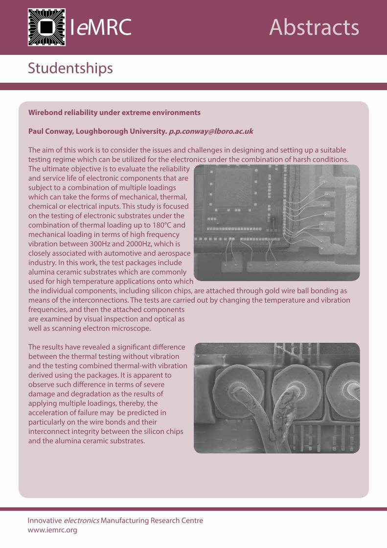
The aim of this work is to consider the issues and challenges in designing and setting up a suitable testing regime which can be utilized for the electronics under the combination of harsh conditions. The ultimate objective is to evaluate the reliability and service life of electronic components that are subject to a combination of multiple loadings which can take the forms of mechanical, thermal,chemical or electrical inputs. This study is focused on the testing of electronic substrates under the combination of thermal loading up to 180°C and mechanical loading in terms of high frequency vibration between 300Hz and 2000Hz, which is closely associated with automotive and aerospaceindustry. In this work, the test packages include alumina ceramic substrates which are commonly used for high temperature applications onto which the individual components, including silicon chips, are attached through gold wire ball bonding as means of the interconnections. The tests are carried out by changing the temperature and vibrationfrequencies, and then the attached components are examined by visual inspection and optical as well as scanning electron microscope.
The results have revealed a signifi cant diff erence between the thermal testing without vibration and the testing combined thermal-with vibration derived using the packages. It is apparent to observe such diff erence in terms of severe damage and degradation as the results of applying multiple loadings, thereby, the acceleration of failure may be predicted in particularly on the wire bonds and their interconnect integrity between the silicon chips and the alumina ceramic substrates.

Abstracts
IeMRC
Innovative electronics Manufacturing Research Centrewww.iemrc.org
Studentships
Fusion of Ultrasound and X-ray Data for Inspection of Modern Microelectronic Packages
David Harvey, Liverpool John Moores University. [email protected]
X-ray inspection and Acoustic micro imaging (AMI) techniques are the principal non-destructive test-ing techniques for evaluating the internal defects of solder joints, as they can penetrate through the component to image the hidden solder joints. However, X-ray inspection and AMI are complementary;each technology has distinct discriminating features and is good at inspecting for certain defects. For example, AMI is an eff ective approach for detecting gap-type defects such as voids, delaminations, disband and thin cracks due to strong refl ections of ultrasound at a solid-air interface. These defects are diffi cult to fi nd by X-ray inspection owing to low contrast. On the other hand, X-ray inspection is able to identify volumetric defects such as solder bridges and broken wires, which are hard to detect by AMI. Penetration of AMI through several layers of dissimilar materials is a problem that needs asolution, whereas X-ray penetration is generally good but without the discrimination accuracy. There-fore, inspection of fl ip-chip and BGA solder joints, and the internal structures of new 3D electronic products remains a signifi cant challenge to current testing techniques.
The best source data from x-ray and ultrasound (AMI) 3D images has been acquired and methods for 3D image registration surveyed, developed and implemented. The second stage has been the investi-gation and evaluation of several fusion approaches at both the pixel and feature level.
The key here has been to preserve independent features from each image whilst uncovering new fea-tures from the fused images. The fi nal stages have assessed performance on real parts from a manu-facturing line, from the fi eld failures and through accelerated ageing.

Based at:Wolfson School of Mech. & Manufact. Eng.,Loughborough University,Loughborough. LE11 3TUwww.iemrc.orgTwitter: @iemrcEmail: [email protected] Supported & funded by: