ABSTRACT - spie.org
13
Photomask Photomask BACUS—The international technical group of SPIE dedicated to the advancement of photomask technology. N • E • W • S november 2018 Volume 34, Issue 11 INDUSTRY BRIEFS —see page 12 CALENDAR For a list of meetings —see page 13 Take A Look Inside: WEREWOLF – Sensitivity optimization for early 7 nm EUV masks using an optical 19x nm inspection system Karen Badger, GLOBALFOUNDRIES, 1000 River Street, Essex Junction, VT, 05452 Masashi Yonetani, Yusuke Toda, Masayuki Kagawa, Toppan Photomasks Inc., 1000 River Street, Essex Junction, VT, 05452 Takeshi Isogawa, Toppan Printing Co., Ltd. 21-33 Nobidome 7-chome, Niiza-shi, Saitama 352-8562 Jan Heumann, Advanced Mask Technology Center, Rähnitzer Allee 9, Dresden, 01109 ABSTRACT EUV (Extreme Ultraviolet) lithography is one of the key enabling techniques for imaging 7-nm node and beyond wafer technologies. To ensure mask quality levels will support High Volume Manufacturing (HVM), all “defects that matter”, must be identified and screened out before shipment to the wafer fab. Mask defects that matter are the ones that print during exposure at 13.5 nm wavelength. To support EUV development and production schedules, mask defectivity must be reduced to be at or near the optical defect levels. This task is complicated by the fact that actinic EUV mask inspectors are not cur- rently available. In the absence of these EUV inspection tools, all available methods for detecting and characterizing defects must be deployed. Based on extensive deployment and on its record for reasonable throughput, 19x nm wavelength in- spection is one of the strongest candidates available today for the initial EUV mask inspection approach. Figure 1. Availability of EUV mask inspection equipment, versus technology roadmap.
Transcript of ABSTRACT - spie.org

PhotomaskPhotomaskBACUS—The international technical group of SPIE dedicated to the advancement of photomask technology.
N • E • W • S
november 2018 Volume 34, Issue 11
Industry BrIefs—see page 12
CalendarFor a list of meetings —see page 13
Take A Look Inside:
WEREWOLF – Sensitivity optimization for early 7 nm EUV masks using an optical 19x nm inspection system Karen Badger, GLOBALFOUNDRIES, 1000 River Street, Essex Junction, VT, 05452
Masashi Yonetani, Yusuke Toda, Masayuki Kagawa, Toppan Photomasks Inc., 1000 River Street, Essex Junction, VT, 05452
Takeshi Isogawa, Toppan Printing Co., Ltd. 21-33 Nobidome 7-chome, Niiza-shi, Saitama 352-8562
Jan Heumann, Advanced Mask Technology Center, Rähnitzer Allee 9, Dresden, 01109
ABSTRACTEUV (Extreme Ultraviolet) lithography is one of the key enabling techniques for imaging 7-nm node and beyond wafer technologies. To ensure mask quality levels will support High Volume Manufacturing (HVM), all “defects that matter”, must be identified and screened out before shipment to the wafer fab. Mask defects that matter are the ones that print during exposure at 13.5 nm wavelength. To support EUV development and production schedules, mask defectivity must be reduced to be at or near the optical defect levels. This task is complicated by the fact that actinic EUV mask inspectors are not cur-rently available. In the absence of these EUV inspection tools, all available methods for detecting and characterizing defects must be deployed.
Based on extensive deployment and on its record for reasonable throughput, 19x nm wavelength in-spection is one of the strongest candidates available today for the initial EUV mask inspection approach.
Figure 1. Availability of EUV mask inspection equipment, versus technology roadmap.

EditorialN • E • W • S
BACUS News is published monthly by SPIE for BACUS, the international technical group of SPIE dedicated to the advancement of photomask technology.
Managing Editor/Graphics Linda DeLano
Advertising Melissa Farlow
BACUS Technical Group Manager Marilyn Gorsuch
■ 2018 BACUS Steering Committee ■
PresidentJim N. Wiley, ASML US, Inc.
Vice-PresidentFrank E. Abboud, Intel Corp.
SecretaryLarry S. Zurbrick, Keysight Technologies, Inc.
Newsletter EditorArtur Balasinski, Cypress Semiconductor Corp.
2018 Annual Photomask Conference ChairsEmily Gallagher, IMEC
Jed Rankin, GLOBALGOUNDRIES Inc.
International ChairUwe F. W. Behringer, UBC Microelectronics
Education ChairFrank E. Abboud, Intel Corp.
Members at LargeMichael D. Archuletta, RAVE LLC
Ki-ho Baik, HOYA Corp. USA Peter D. Buck, Mentor Graphics Corp.
Brian Cha, Samsung Electronics Co., Ltd.Derren Dunn, IBM Corp.
Thomas B. Faure, GLOBALFOUNDRIES Inc.Aki Fujimura, DS2, Inc.
Brian J. Grenon, Grenon ConsultingJon Haines, Micron Technology Inc.
Naoya Hayashi, Dai Nippon Printing Co., Ltd. Bryan S. Kasprowicz, Photronics, Inc.
Patrick M. Martin, Applied Materials, Inc. Kent Nakagawa, Toppan Photomasks, Inc.
Jan Hendrik Peters, bmbg consultMoshe Preil, KLA-Tencor Corp.
Stephen P. Renwick, Nikon Research Corp. of AmericaDouglas J. Resnick, Canon Nanotechnologies, Inc.
Thomas Scheruebl, Carl Zeiss SMT GmbHThomas Struck, Infineon Technologies AG
Bala Thumma, Synopsys, Inc.Anthony Vacca, Automated Visual Inspection
Michael Watt, Shin-Etsu MicroSi Inc.
P.O. Box 10, Bellingham, WA 98227-0010 USATel: +1 360 676 3290Fax: +1 360 647 1445
©2018
All rights reserved.
Mask Industry: Up, and To the Right!Aki Fujimura, CEO, D2S, Inc.
As reported in the Industry Briefs section of the October 2018 edition of this newsletter, SEMI reported recently that the overall mask market increased to $3.75B in 2017, a 4.1% compounded annual growth rate (CAGR) for 3 years ending 2017. And, according to two new surveys conducted by the eBeam Initiative and presented last month at the SPIE Photomask Technology Conference in Monterey, CA, mask makers reported a significant increase in mask output this year as compared to last, and industry leaders predict the market growth will continue.
The eBeam Initiative surveys were conducted over the summer, prior to the recent news about capital expenditure reductions in semiconductor manufacturing. However, the two surveys, taken together, do still paint an optimistic picture for the future growth of semiconductor manufacturing – the line on the growth chart is up and to the right. The eBeam Initiative mask makers survey respondents – the same 10 captive and merchant photomask manufacturers who participated in last year’s survey – reported a 27% overall increase in mask output this year as compared to last. Increases were reported in numbers of masks produced at every ground rule, but ≥5nm and <7nm, ≥16nm and <22nm, and ≥65nm and <90nm were particularly pronounced in percentage increases year over year. Respondents reported that lasers wrote 74% of the masks they produced this past year. Overall mask yields have remained steady at 94% over the last two years.
In addition to the increase in the total number of masks written, the average write time required to write masks also increased year to year. Average write time for VSB writers increased from 6.8 hours in the 2017 survey to 8.3 hours in 2018. Average write time for laser writers increased from 1.8 hours to 2.1 hours. Taken together, the total demand for mask writers of every type increased significantly year over year. Mask data volume average also went up substantially for both. Average data volume for VSB writers went up from 0.94 to 1.23 TBytes for VSB writers and from 8 to 19 GBytes for laser writers. Since data volume correlates with inspection and other processing times as well, the overall demand on mask manufacturing equipment increased significantly year to year.
Mask makers did not note an improvement in mask turnaround time. As in previous years, respondents reported that leading-edge ground rules have substantially longer mask turnaround times than the previous generation. Ground rules above and including 130nm have an average turnaround time of 3.2 days, while those below and including 7nm need 11.7 days.
Separately, the eBeam Initiative also conducts an annual industry perceptions survey. Started in 2012, this opinion-based survey is sent to industry luminaries each year to gather the best predictions of industry trends. When asked if the CAGR of 4.1% shown in the SEMI study could be maintained in the future, 95 percent of respondents predicted that the CAGR for overall mask market will be at least 4.1% between 2018 and 2020; more than 50 percent of respondents predicted the CAGR would be higher than 4.1%.
While reported EUV masks still represent a very small percentage of overall mask production, the number of EUV masks reported doubled this year (2185) from last year (1041). The perceptions survey showed 82 percent of respondents predicted that EUV lithography will be used in high-volume manufacturing by 2021, while only 1 percent of respondents predicted it will never happen.
The perception survey showed similar optimism about the adoption of multi-beam mask writers (MBMW): 82 percent of respondents indicated that they believe that MBMW will be used in high-volume manufacturing by the end of 2020.
The time-bound quest for the next technology node requires simultaneous advances in the state-of-the-art in human creation in physics, chemistry, material science, mechanical engineering, computer science and high-performance computing, including deep learning. It is a large-scale team effort involving many, many people, companies, research organizations, universities and government agencies of so many different disciplines, bound together by the common mission to get the next node working on time. At the SPIE Photomask Technology Conference, we get to see the best-of-the-best in human capability. It is great fun to be able to be in the middle of all this action. And even better when we see that growth line going up and to the right!
To view slides that summarize all of the data collected by these surveys go to: http://www.ebeam.org/docs/eBeam-Perception-Survey-2018.pdf and http://www.ebeam.org/docs/eBeam-Mask-Maker-Survey-2018.pdf
However, there are several key challenges with 19x nm optical inspec-tion of EUV masks. Aside from the documented challenges of using a non-actinic wavelength, a key challenge is that the defect sensitivity varies based on pattern sizes and defect types and therefore, a wide range of pattern sizes and defect types need to be used to optimize inspection sensitivity. Through a variety of evaluations on simple test patterns, it has been confirmed that a combination of multiple focus offsets and polarization settings enables adequate sensitivity to meet early sensitivity requirements for 7 nm EUV production masks. As the result, focus offsets and polarization settings could be optimized to successfully develop new inspection recipes that could meet a target defect criteria with multi-pass inspection.[1]
In this study, we will show inspection results of programmed defect macros (PDMs) based on actual EUV device constructs. Then, it will be discussed whether a combination of multiple focus offsets and polarizations is an effective approach to increase defect sensitivity on device patterns through the analysis of PDMs. We will demonstrate how inspection parameter optimization can be done to tailor 19x nm inspection to EUV device designs and what defect sizes and types are detectable with a 19x nm inspection system to assess capability for meeting the 7nm node development and production requirements.
1. IntroductionAs technology evolves, advanced imaging techniques become more important to resolve smaller and smaller features on wafer. One of the
most promising approaches to resolving these images for 7 nm node and beyond is EUV (Extreme Ultraviolet) lithography. Producing defect free masks for this advanced technology approach is complicated by the fact that the availability of 13.5 nm wavelength scanners has far sur-passed the timing of 13.5 nm wavelength mask inspection equipment.
Figure 1 shows an estimation of the timing and capability for each of the three inspection candidates for EUV mask inspection: 19x nm Optical, e-beam and actinic. While the industry awaits the ar-rival and integration of actinic mask inspection capability, measures must be taken to determine what is possible on currently available equipment[1-3]…specifically, what levels of inspectability and defect sensitivity can be achieved on 19x optical and e-beam inspection equipment. 19x optical inspection has a well-established history and reputation for sensitivity and inspectability for optical masks built on various attenuators and for critical dimensions through 7 nm node—at an acceptable rate of throughput[4-7]. Over time, extensive optics and algorithm improvements have been implemented on 19x nm inspec-tors to improve EUV mask inspectability and sensitivity[8-10], but the question remains as to whether they are capable of finding all wafer printable defects in both the absorber and multi-layers. In Figure 1 below, it is apparent that 193 nm optical inspection will become less effective with the introduction of assist features, so at best, may be usable at a somewhat reduced sensitivity through 2019, and poten-tially through 2020 if assist feature desense is acceptable. E-beam inspectors are specifically being introduced for the inspection of EUV masks, and provide an advantage over optical inspection equipment
Figure 3. WEREWOLF PDMs 7 nm hole and line/space designs and substrate configuration.
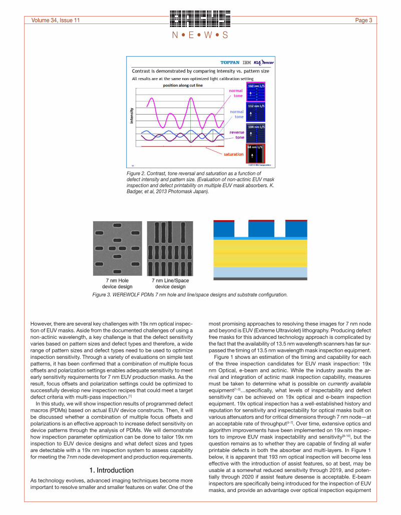
Figure 2. Contrast, tone reversal and saturation as a function of defect intensity and pattern size. (Evaluation of non-actinic EUV mask inspection and defect printability on multiple EUV mask absorbers. K. Badger, et al, 2013 Photomask Japan).
Volume 34, Issue 11 Page 3
N • E • W • S

Figure 4. WEREWOLF PDMs - Defects of Interest.
in that they are able to achieve higher defect sensitivity on smaller critical dimensions due to the smaller beam size. Unfortunately, this improved capability typically comes at the cost of very long inspec-tion times and low throughput, charging issues with the black border, and the total inability to see into the multi layer. Similar to the 19x nm inspectors, additional work is also required relative to the detection of all wafer-printable defects by e-beam inspectors. On the other hand, Actinic database pattern inspection, by its very nature, is the best solution for detecting wafer-printable defects…except for the fact that it is not currently available.
It has become evident that EUV masks will require more advanced
approaches to mask inspection. The absence of actinic inspection capability is compounded by the fact that the EUV substrate is not transmissive (due to the chrome backing layer), and therefore must be inspected only with reflected light. A second complication is the nature of the substrate itself, consisting of the LTEM (Low Thermal Expansion Material) substrate, backside conductive layer, front-side reflective stack of 40 pairs of Mo/Si bilayers, a Ru protective cap, and the Ta-based absorber material. Defects on…or in, any of these layers could print on wafer. Again, actinic inspection is expected to see into all of these layers and provide sensitivity enough to achieve the detection of wafer-printable defects, however, current 19x nm wavelengths are
Figure 5. Focal Planes definition.
Page 4 Volume 34, Issue 11
N • E • W • S

able to penetrate only the top 3-4 layers, and e-beam is not expected to penetrate the Mo/Si bilayers at all.
Considering the non-availability of actinic inspectors at this time, and the relatively recent introduction of e-beam tools that will require extensive evaluation and optimization, the focus of this paper will be on steps that may be taken on 19x nm inspection equipment to potentially improve the detection capability of absorber defects that may print on wafer.
2. Analysis of Present StateBefore we begin this evaluation, let us first point out a few conflicts that exist between the 19x nm inspection wavelength and EUV mate-rial properties.
19x nm optical mask inspection requires at least 65% contrast between the absorber and the multilayer in order to achieve optimum sensitivity and inspection speed. The index of refraction for the 193 nm wavelength is not even close to that of EUV. The current absorber
Figure 7. Hole Layer PDM inspected with Circular Polarization and eight different focal planes.
Figure 6. Polarization definition.
Volume 34, Issue 11 Page 5
N • E • W • S

stack is approximately 37% reflective at 19x nm wavelength, while the multilayer is approximately 60% reflective. This results in a contrast of approximately 24% versus a target of 65%. In addition, Figure 2 demonstrates two optical phenomena at 19x nm wavelength: image tone reversal, which occurs at a specific image size and effectively lowers the intensity of the defect signal, and saturation or poor resolu-tion, which happens near the 68 nm point.
In previous work, it was determined that reducing base pattern contrast is not the right solution toward the goal of maximizing defect signal, but rather, improved defect signals are better achieved through adjustments or combinations of focus and polarization[11]. These results confirm that no single polarization or focus setting is able to detect all of the defects, but that improved sensitivity can be achieved through a combination of polarization and focus settings.
Figure 8. Line/Space Layer PDM – inspected with Circular Polarization and eight different focal planes.
Figure 9. Impact of focus offset on defect signals (Hole layer - left, Line/Space - right).
Page 6 Volume 34, Issue 11
N • E • W • S
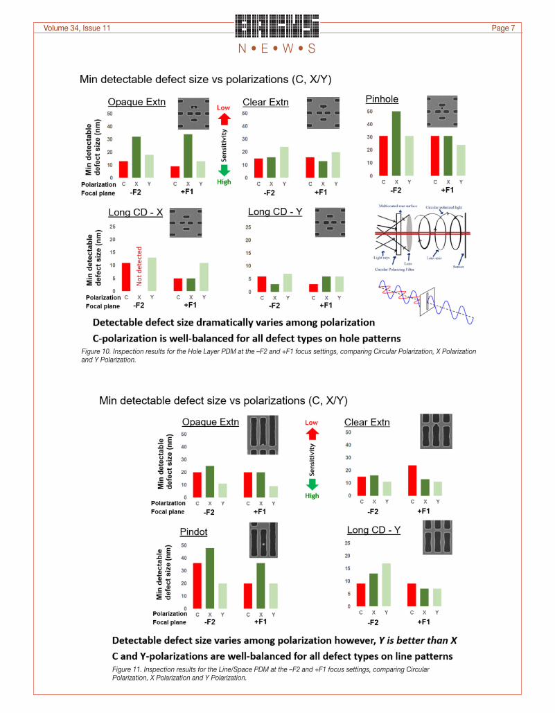
Figure 10. Inspection results for the Hole Layer PDM at the –F2 and +F1 focus settings, comparing Circular Polarization, X Polarization and Y Polarization.
Figure 11. Inspection results for the Line/Space PDM at the –F2 and +F1 focus settings, comparing Circular Polarization, X Polarization and Y Polarization.
Volume 34, Issue 11 Page 7
N • E • W • S

3. Test VehiclesKnowing that defect sensitivity can be influenced through a combina-tion of polarization and focus settings, the primary goal of this evalu-ation was not only to verify how much improved defect sensitivity was possible, but to determine whether that improved sensitivity as adequate for all wafer printable defects on a 7 nm EUV product design. To achieve that goal, new programmed defect test macros (PDMs) were designed. That PDM is named WEREWOLF (World-class Euv REticle for Widespread Optimization, Learning and Feasibility study). WEREWOLF was designed to specifically understand absorber defect sensitivity and printability on actual 7 nm node product designs. Figure 3 provides a visual representation of the hole and line/space design types and substrate configuration. Figure 4 provides examples of the typical programmed defects available for analysis.
Multiple focus offsets and polarizations were used in this evaluation. As is traditionally done, best focus is defined as the surface on which the 19x tool produces the sharpest image profile for the absorber. As seen in Figure 5, for the purpose of this study, Zero focus is placed on the surface of the absorber, Negative focus is positioned away from the absorber, and Positive focus is positioned toward the Multilayer.
Figure 6 demonstrates the two types of polarization that were used in this study. Circular Polarization, or C-Pol is generally used for hole layers, and focuses the light rays in a circular motion toward the filter. X-Y Polarization are generally used for line/space layers. The X or Y filter transmits only the component of the wave parallel to its axis, and reduces the intensity of any light not parallel to its axis. For the purpose of this evaluation, both pattern types were inspected using both Circular and X-Y polarizations
4. The Impact of Focus and Polarization on Defect Sensitivity
The Hole layer PDM was inspected with eight different focus offsets, and with Circular Polarization. The eight focus offsets include best focus (denoted by 0), three negative offsets (denoted by –F1, -F2, -F3), and four positive offsets (denoted by +F1, +F2, +F3, +F4). All inspec-tions used exactly the same defect sensitivity settings. The sensitivity results can be seen in Figure 7. As can be seen, the smallest detectable defect size changes dramatically with a fixed Circular polarization and varied focus. What is also clear, is that no one focal plane finds all of the smallest defect sizes, however the –F1, 0 and +F1 focal planes are more sensitive than the other focal planes tested. What is also implied is that all three of these inspections taken together—one at –F1 focus and the others at 0 focus and +F1 focus—are capable of finding the smallest detectable defects at the settings used for this 19x nm optical inspection. It is possible, that in order to achieve maximum sensitivity for the smallest detectable defects by type, multiple inspections at multiple focal planes may be required.
Even though Circular Polarization is typically used on Hole layer pat-terns, tests were conducted to look at Circular Polarization combined with multiple focus offsets on the Line/Space pattern as well. The same eight focus offsets were used. The sensitivity results can be seen in Figure 8. As with the Hole layer pattern, the smallest detectable defect size changed dramatically with a fixed Circular polarization and varied focus. In this case, the –F1, 0 and +F1 focus offset settings provide the best combined sensitivity for all defect types on the Line/Space PDM. Again, as was the case with the Hole layer PDM, maximum sensitivity for the smallest detectable defects by type was achievable with Circular Polarization combined with multiple focal planes.
Figure 9 demonstrates the impact of the different focal planes on defect signal for both the Hole layer and Line/Space layer PDM’s. As can be seen, the defect signal varies slightly with focal plane, and
Figure 12. Single pass sensitivity versus multiple combinations of polarization and focus offsets.
Page 8 Volume 34, Issue 11
N • E • W • S

for nearly all defect types analyzed, a combination of multiple focus offsets provide the best sensitivity.
The next phase of this evaluation was to determine if defect sensi-tivity could be influenced by changing the polarization. To that end, X Y Polarization, along with two of the original eight focal planes, was used to inspect both the Hole layer and Line/Space layer PDM’s, and then a comparison was made to those same two focus settings from the Circular Polarization runs on both PDM’s. Figure 10 provides the inspection results for the Hole Layer PDM at the –F2 and +F1 focus settings, comparing Circular Polarization, X Polarization and Y Polar-ization. The defect types evaluated are opaque and clear extensions, pinholes and oversized critical dimensions (X and Y).
For the Hole layer PDM, Circular polarization provided overall better sensitivity than X or Y polarization, however, what is interesting to note, is that the Y polarization on the Hole PDM provided better sensitivity results on opaque edge defects and the X polarization provided bet-ter sensitivity results on clear edge defects. For optimum sensitivity, combined inspections using all three of the polarizations provides the best sensitivity for these two focus offset settings.
Figure 11 shows similar results for the same three polarizations and focus settings on the Line/Space PDM. The defect types evaluated here are opaque and clear extensions, pindots and oversized critical dimension (Y axis only).
For the Line/Space results, the Y polarization provided better sen-
Figure 13. Detectability by focus offset and Circular Polarization versus EUV AIMS™ Printability.
Figure 14. EUV defect signal and printability as a function of defect size.
Volume 34, Issue 11 Page 9
N • E • W • S

sitivity than the X Polarization, regardless of defect contrast, and it provided better sensitivity than the Circular polarization for all but one defect type on the –F2 focus offset (long CD). For optimum sensitivity, combined inspections for Circular and Y polarization provides the best sensitivity for these two focus offset settings. Note that if this pattern was rotated 90-degrees, we would expect X polarization to provide better sensitivity than Y polarization.
Figure 12 describes the overall take-away from the focus offset and polarization study…that using a single polarization and single focus offset will provide a certain level of defect sensitivity for EUV masks, however, using multiple focus offsets and polarizations in combina-tion with each other can improve overall sensitivity as small as 15 nm for opaque and clear extensions, and as small as 7 nm for critical dimension errors.
It should be noted that the results depicted in Figure 12 reflect all of the focus offsets and polarizations combined (Circular Polarization, X Polarization, Y Polarization, -F3, -F2, -F1, 0, +F1, +F2, +F3, +F4 focus offsets) with all inspections run at higher-than-normal sensitivity set-tings. Obviously, this is not feasible in a high-volume manufacturing mode for two reasons…first, it represents up to 24 inspections on the same mask, and second, at higher-than-normal detector settings, there will undoubtedly be excessive nuisance detections in addition to the real, programmed defects. What is feasible, however, is determining the exact wafer-printable size by defect type, and then determining a fewer number of focus offset and polarization combinations…and optimized detector settings, that will come closest to achieving level of sensitivity required to detect them.
5. Printability ResultsWe began this study to determine if it was possible to extend the capability of existing 19x nm optical inspection equipment to at least improve the ability to detect wafer printable absorber defects. We have demonstrated thus far that it is indeed possible to improve overall defect sensitivity by combining multiple polarizations and focus offset settings, however, the question remains—can we realize enough improvement to carry us over to the next generation inspection capability? To answer that question, we engaged in two printability studies: one using EUV simulation, and the other, using EUV AIMS™.
Figure 13 provides the EUV AIMS™ printability results for the Hole Layer PDM, on the Opaque Extension, Clear Extension, Long CD X and Long CD-Y defect types. To reiterate, these defects were inspected at eight different focal planes, using high sensitivity defect detectors. The red lines represent the 10% CD error on wafer target for each defect type. As demonstrated in Figure 12, several of the focal planes are able to detect wafer printable defects. In some cases—specifically for the Long CD-Y defect type—the inspection was able to detect defects significantly smaller than the 10% CD print line. This additional sensitivity provides room to desense to more inspectable detectors for this defect type without losing the required sensitivity to detect printable defects.
One thing to note is that the linear defect sizes for the edge and CD defects are smaller than 20 – 25 nm range generally anticipated for 7 nm node EUV masks. This very well could be due to the design type and design MEEF. This further accentuates the need for actinic ‘litho-based’ inspection capability.
Figure 14 provides a comparison between SEM defect size, EUV AIMS™ printability and the signal strength at inspection for defects that fail the 10% printability target, and those that do not. All of these defects were detected during the high-sensitivity inspection. Signal strength is defined as the defect ‘residual’ seen at inspection.
6. Summary
Defect Sensitivity versus Wafer PrintabilityThis study has demonstrated that a 19x nm inspection system is capable of detecting EUV mask defects that fail a 10% CD error specification on wafer, and in some cases, is able to detect defects that cause far smaller than 10% CD error on wafer. Keep in mind, that this evaluation only addresses absorber defects visible to a 19x nm optical mask inspection system and does not address multi-layer defects. The data in this evaluation represents defects detected at high sensitivity settings and uses multiple focus offsets and polariza-tion conditions. The conditions presented here may not be applicable to high-volume manufacturing as it may require multiple inspection passes and significant optimization to improve inspectability. In addi-tion, the wafer-printable linear defect size is smaller than anticipated for 7 nm EUV, and may be a factor of image size, image type and MEEF.
Defect Sensitivity Improvements19x nm defect inspection is the strongest candidate for initial EUV production until high-throughput E-Beam or Actinic inspection is ready. In the meantime, this study has shown that the overall sensitivity of the 19x nm optical inspection systems can be improved for EUV mask inspection by optimizing combinations of focus offsets and polariza-tion settings. New inspection recipes could be established to reflect this new sensitivity. Through multi-pass inspection, defect sensitivity as small as 15 nm for point defects and 7 nm for CD errors can be achieved on 7 nm EUV hole and line/space designs. Based on this approach, this could extend the useful life of 19x nm optical inspection tools through 7 nm EUV production, and 5 nm EUV development for the detection of absorber defects only. The 19x nm optical inspection system can be a valuable part of an inspection approach that also uses actinic blank inspection tools for multiplayer defect detection, and defect avoidance techniques to minimize the impact of absorber and multi-layer defects on printed images.
Throughput and OptimizationA major recommendation of this study is to use multiple focus offsets, combined with multiple polarizations in order to approach—and in some cases—achieve or even exceed wafer printable defect sensi-tivity on a 19x nm optical mask inspection tool. Two questions come to mind relative to this recommendation…first, is this cost effective, and second, how does this impact turnaround time? If you consider three focus offsets times two polarizations, this equals a worse-case scenario of six inspections. Assuming each inspection requires 2.5 hours of tool time for a full-field inspection area of approximately 100 mm x 130 nm, these six inspections will use approximately 15 hours of time. Now consider that one full-field inspection at current e-beam inspection run times would require weeks to complete, 15 hours of 19x nm optical inspection tool time is a cost-effective way to achieve printable, or near-printable defect sensitivity while turnaround time issues are being addressed on e-beam inspection tools.
Optimization can be achieved in several ways. One is to optimize inspection settings to minimize nuisance detections, while keeping in mind that this might result in desensing some features such as SRAFS, corners, notches and numbs in order to maintain high sensitivity on primary lines and spaces. A second way to optimize is to tailor the selection of focus-offset settings to match a given process capability. For example, if a process seldom produces clear defects, it may be possible to eliminate focus offset settings that optimize clear defect sensitivity and still achieve printable sensitivity on other defect types, but with fewer inspections.
Page 10 Volume 34, Issue 11
N • E • W • S

7. AcknowledgmentsThe authors would like to thank the following for their contributions to this paper: Jed Rankin of GLOBALFOUNDRIES, and Shinji Akima of TOPPAN PHOTOMASKS for technical advice and discussion. Kazunori Seki of TOPPAN PHOTOMASKS for the groundwork load during the evaluation and writing of the 2017 Photomask Japan Best Paper, “Minimizing Tone Reversal During 19x Mask Inspection.” John Leonard and Chad Normand of GLOBALFOUNDRIES for data collec-tion and technical discussion. Grizelda Kersteen of Carl Zeiss SMT GmbH for EUV AIMSTM support. Finally we would like to thank the GLOBALFOUNDRIES, ADVANCED MASK TECHNOLOGY CENTER and TOPPAN management and technical teams for their support of this project.
8. References[1] Kazunori Seki et al., “Shedding light on EUV inspection,” Proc. SPIE
8841, 844114 (2012). [2] Karen Badger et al., “Illuminating EUVL mask defect printability,” Proc.
SPIE 8522, 852201 (2012). [3] Zhengqing John Qi et al., “Impact of EUV photomask line edge
roughness on wafer prints,” Proc. SPIE 8522, 85222H (2012). [4] Masato Naka, Akihiko Ando, et al., “DUV inspection beyond optical
resolution limit for EUV mask of hp 1X nm,” Proc. SPIE 10451 (2017). [5] Hiromu Inoue, Nobutaka Kikuiri, et al., “DUV inspection tool application
for beyond optical resolution limit pattern,” Proc. SPIE 9635 (2015). [6] Ching-Fang Yu et al., “Inspection of advanced computational
lithography logic reticles using a 193-nm inspection system,” Proc. SPIE 7823, 78232F (2010).
[7] Thomas Faure et al., “Development of a new high transmission phase shift mask technology for 10 nm logic node,” Proc. SPIE 9984, 998402 (2016).
[8] Daniel Wack., “EUV mask inspection with 193 nm inspector for 32 and 22 nm HP,” Proc. SPIE 7748, 77481Y (2010).
[9] Kazunori Seki et al., “Reflecting on inspectability and wafer printability of EUV mask absorbers,” Proc. SPIE 8800, 88800S (2013).
[10] Karen Badger et al., “Illuminating extreme ultraviolet lithography mask defect printability,” J. Micro/Nanolithogr., MEMS, MOEMS 12, 021004 (2013).
[11] Seki, K. et al., “Minimizing ‘Tone Reversal’ During 19x nm Mask Inspection,” PMJ2018 Photomask Japan, Proc. SPIE 10807, 108070D.
Volume 34, Issue 11 Page 11
N • E • W • S

N • E • W • S
Sponsorship OpportunitiesSign up now for the best sponsorship
opportunities
Photomask 2018 — Contact: Melissa Farlow,
Tel: +1 360 685 5596; [email protected]
Advanced Lithography 2018 — Contact: Teresa Roles-Meier,
Tel: +1 360 685 5445; [email protected]
Advertise in the BACUS News!
The BACUS Newsletter is the premier publication serving the photomask industry. For information on how to advertise, contact:
Melissa Farlow, Tel: +1 360 685 5596 [email protected]
BACUS Corporate Members
Acuphase Inc.American Coating Technologies LLCAMETEK Precitech, Inc.Berliner Glas KGaA Herbert Kubatz
GmbH & Co.FUJIFILM Electronic Materials U.S.A., Inc.Gudeng Precision Industrial Co., Ltd.Halocarbon ProductsHamaTech APE GmbH & Co. KGHitachi High Technologies America, Inc.JEOL USA Inc.Mentor Graphics Corp.Molecular Imprints, Inc.Panavision Federal Systems, LLCProfilocolore SrlRaytheon ELCAN Optical TechnologiesXYALIS
■ Intel Denies Media Reports Claiming it Cancelled its 10nm Process
Joel HruskaIntel’s 10nm process has been bedeviled by delays and problems — the node is years late already, and it may not debut at volume until Q4 2019. New media reports suggest that Intel has cancelled the node completely, while Intel itself denies that charge. Unfortunately, it’s not possible to see the actual evidence for its argument. But the better question to ask is this: Regardless of whether Intel canceled its previous 10nm process, would Intel walk away from being a leading-edge foundry? And the answer there is an obvious “No.” In this context, ” canceling” 10nm could mean something more akin to “drawing up a new plan for future node progression.” There’s too much at stake as far as Intel’s perceived manufacturing prowess.
If the rumor is right, we’ll likely hear about it before long. Intel, having previously repeatedly committed to a 10nm ramp in Q4 2019 will have to publicly notify its partners and investors about any delay, just as it notified them about the previous ones. The more likely for Intel is to still push forward with a “10nm” node with different characteristics —relaxed than the company’s incredibly ambitious hyperscaling project.
https://www.extremetech.com/computing/279306-intel-denies-media-reports-claiming-it-cancelled-its-10nm-process
■ EUV and Expanding the SSD Ecosystem
Tom CoughlinSamsung made some significant announcements at its Samsung Tech Day this week. This included 7nm lithographic processes using Extreme Ultraviolet (EUV), 500+ layer NAND in the future, a second generation Z-NAND and HBM, a smart SSD with an FPGA on the board, KV SSDs and a future native ethernet NVMe SSD and more.
Samsung announced that it has completed all process technology development and has started wafer production of its revoluntionary process node, 7LPP, the 7-nanometer (nm) LPP (Low Power Plus) with extreme ultraviolet (EUV) lithography technology. According to the company, «The introduction of 7LPP is a clear demonstration of Samsung Foundry’s technology roadmap evolution and provides customers with a definite path to 3nm.
https://www.forbes.com/sites/tomcoughlin/2018/10/19/euv-and-expanding-the-ssd-ecosystem/#2f5ffb041ffe
■ Advanced Technology Key to Strong Foundry Revenue Per Wafer
The average revenue generated from processed wafers among the four biggest pure-play foundries (TSMC, GlobalFoundries, UMC, and SMIC) is expected to be $1,138 in 2018, when expressed in 200mm-equivalent wafers, which is essentially flat from $1,136 in 2017, according to a new analysis by IC Insights. The average revenue per wafer among the Big 4 foundries peaked in 2014 at $1,149 and then slowly declined through last year, based on IC Insights’ extensive part-two analysis of the integrated circuit foundry business in the September Update to The 2018 McClean Report.
Although the average revenue per wafer of the Big 4 foundries is forecast to be $1,138 this year, the amount generated is highly dependent upon the minimum feature size of the IC processing technology. In 2Q18, there was more than a 16x difference between the 0.5µ 200mm revenue per wafer ($370) and the ≤20nm 300mm revenue per wafer ($6,050). Even when using revenue per square inch, the difference is dramatic ($7.41 for the 0.5µ technology versus $53.86 for the ≤20nm technology). Since TSMC gets such a large percentage of its sales from ≤45nm production, its revenue per wafer is expected to increase by a compound annual growth rate (CAGR) of 2% from 2013 through 2018 as compared to a -2% CAGR for the total revenue per wafer average of GlobalFoundries, UMC, and SMIC during this same time period.
https://electroiq.com/2018/10/advanced-technology-key-to-strong-foundry-revenue-per-wafer/
Page 12 Volume 34, Issue 11
N • E • W • S
Industry Briefs

SPIE is the international society for optics and photonics, an educational not-for-profit organization founded in 1955 to advance light-based science, engineering, and technology. The Society serves nearly 264,000 constituents from 166 countries, offering conferences and their published proceedings, continuing education, books, journals, and the SPIE Digital Library in support of interdisciplinary information exchange, professional networking, and patent precedent. SPIE provided more than $4 million in support of education and outreach programs in 2017. www.spie.org
International HeadquartersP.O. Box 10, Bellingham, WA 98227-0010 USA Tel: +1 360 676 3290 Fax: +1 360 647 [email protected] • www.SPIE.org
Shipping Address1000 20th St., Bellingham, WA 98225-6705 USA
Managed by SPIE Europe 2 Alexandra Gate, Ffordd Pengam, Cardiff, CF24 2SA, UK Tel: +44 29 2089 4747 Fax: +44 29 2089 [email protected] • www.spieeurope.org
2019
Photomask Japan16-18 April 2019PACIFICO YokohamaYokohama, Japan www.photomask-japan.org
SPIE Advanced Lithography24-28 February 2019 San Jose Marriott and San Jose Convention Center San Jose, California, USA
The 35th European Mask and Lithography Conference, EMLC 201917-19 June 2019Hilton Hotel DresdenDresden, Germany
Corporate Membership Benefits include:■ 3-10 Voting Members in the SPIE General Membership,
depending on tier level
■ Subscription to BACUS News (monthly)
■ One online SPIE Journal Subscription
■ Listed as a Corporate Member in the BACUS Monthly Newsletter www.spie.org/bacushome
C A L E N D A R
About the BACUS GroupFounded in 1980 by a group of chrome blank users wanting a single voice to interact with suppliers, BACUS has grown to become the largest and most widely known forum for the exchange of technical information of interest to photomask and reticle makers. BACUS joined SPIE in January of 1991 to expand the exchange of information with mask makers around the world.
The group sponsors an informative monthly meeting and newsletter, BACUS News. The BACUS annual Photomask Technology Symposium covers photomask technology, photomask processes, lithography, materials and resists, phase shift masks, inspection and repair, metrology, and quality and manufacturing management.
Individual Membership Benefits include:■ Subscription to BACUS News (monthly)
■ Eligibility to hold office on BACUS Steering Committee
www.spie.org/bacushome
You are invited to submit events of interest for this calendar. Please send to [email protected]; alternatively,
email or fax to SPIE.
h
h
Join the premier professional organization for mask makers and mask users!
h
Volume 34, Issue 11 Page 13
N • E • W • S