A1335: Datasheet Addendum: Programming Reference€¦ · Precision Hall-Effect Angle Sensor IC with...
101
Precision Hall-Effect Angle Sensor IC with I 2 C, SPI, and SENT Interface A1335 A1335-ADD1 Datasheet Addendum: Programming Reference This addendum provides programming instructions and reference tables to the general sales datasheet (A1335) for this device. For parameters not listed in this addendum, refer to the general sales datasheet. In the event of a conflict between this addendum and the general sales datasheet, this addendum takes precedence. Table of Contents Programmable Functionality 2 Interface Structure 3 Primary Serial Interface Registers Reference 5 I 2 C Interface Description 17 Writing to Base Addresses 18 Reading from Base Addresses 20 I 2 C Data Redundancy Mode 20 SPI Interface 21 SPI Interface Timing 21 SPI Message Frame Size 22 Write Cycle Overview 23 Read Cycle Overview 23 Manchester Serial Interface 24 Entering Manchester Communication Mode 24 Transaction Types 24 Reading Data Using Manchester Encoding 25 Error Checking 25 Manchester Message Structure 26 Manchester Interface Reference 27 Extended Access Protocol 31 Writing to Extended Addresses 31 Reading from Extended Addresses 33 Extended Access Command Set 35 SRAM Description and Programming 41 Dual Purpose Registers 41 Angle Resolution for SRAM 41 SRAM Register Reference 42 EEPROM Description and Programming 58 Programming EEPROM 58 Unlocking EEPROM 58 Dual Purpose Registers 58 Self-Test Options 59 Configuration Flags 59 Angle Resolution for EEPROM 59 EEPROM Register Reference 60 Appendix A: SENT Output Description A-1
-
Upload
truongduong -
Category
Documents
-
view
239 -
download
3
Transcript of A1335: Datasheet Addendum: Programming Reference€¦ · Precision Hall-Effect Angle Sensor IC with...

Precision Hall-Effect Angle Sensor ICwith I2C, SPI, and SENT Interface
A1335
A1335-ADD1
Datasheet Addendum: Programming Reference
This addendum provides programming instructions and reference tables to the general sales datasheet (A1335) for this device.
For parameters not listed in this addendum, refer to the general sales datasheet. In the event of a conflict between this addendum and the general sales datasheet, this addendum takes precedence.
Table of ContentsProgrammable Functionality 2Interface Structure 3Primary Serial Interface Registers Reference 5I2C Interface Description 17
Writing to Base Addresses 18Reading from Base Addresses 20I2C Data Redundancy Mode 20
SPI Interface 21SPI Interface Timing 21SPI Message Frame Size 22Write Cycle Overview 23Read Cycle Overview 23
Manchester Serial Interface 24Entering Manchester Communication Mode 24Transaction Types 24Reading Data Using Manchester Encoding 25Error Checking 25Manchester Message Structure 26Manchester Interface Reference 27
Extended Access Protocol 31Writing to Extended Addresses 31Reading from Extended Addresses 33Extended Access Command Set 35
SRAM Description and Programming 41Dual Purpose Registers 41Angle Resolution for SRAM 41SRAM Register Reference 42
EEPROM Description and Programming 58Programming EEPROM 58Unlocking EEPROM 58Dual Purpose Registers 58Self-Test Options 59Configuration Flags 59Angle Resolution for EEPROM 59EEPROM Register Reference 60
Appendix A: SENT Output Description A-1

Precision Hall-Effect Angle Sensor ICwith I2C, SPI, and SENT InterfaceA1335
2Allegro MicroSystems, LLC115 Northeast CutoffWorcester, Massachusetts 01615-0036 U.S.A.1.508.853.5000; www.allegromicro.com
A1335-ADD1
Programmable FunctionalityThe A1335 provides additional functionality through the primary serial interface, as described in this addendum. Certain of these functions can be performed only while the the processor is not processing angle data (Idle mode), others only while angle data is being processed (Run mode), and some can be performed in either mode. A guide is provided in Table 1. The operating mode is set using the CDS field of the 0x1E register in the Primary Serial Interface.
SRAM based memory is volatile and gets cleared on a reset or repower. EEPROM-based memory is non-volatile and is perma-nent. Parameters can be tested using SRAM memory and then permanently written to EEPROM after all final settings have been finalized.
Table 1: Modes for Programmable FunctionsActivity Idle Mode Run Mode
Read EEPROM
Write EEPROM –
Process Angles –
Read SRAM
Write SRAM
Change ORATE –
Read ORATE
Self Tests –
Set Serial I/O Parameters
Read Errors

Precision Hall-Effect Angle Sensor ICwith I2C, SPI, and SENT InterfaceA1335
3Allegro MicroSystems, LLC115 Northeast CutoffWorcester, Massachusetts 01615-0036 U.S.A.1.508.853.5000; www.allegromicro.com
A1335-ADD1
Serial Interface Primary Registers(Base Addresses)
Additional Registers(Extended Addresses)
Addressand Data
I/O
02:03
08:09
04:07
0A:0B
0C:0D
0E:11
1E:1F
20:21
22:23
24:25
26:27
28:29
34:35
36:37
Extended Write addresses
Extended Read addresses
Extended Write data
Extended Read data
Extended Write control and status
Extended Read control and status
Current data read out
Device control
Device statusDevice error status
Extended error status
Error masks
Extended error masks
Temperature read out
EWA, EWD, ERA and ERDare used to access the extended address that contain EEPROM and SRAM
EWA
EWCS
EWD
ERA
ERCS
ERD
CTRL
ANG
STA
ERR
XERR
TSEN
ERM
EXERM
Table 2: Primary Serial Interface Registers (Reserved Registers Not Shown)Address*
(Hex) Name Usage
02:03 EWA Extended Write Address
04:07 EWD Extended Write Data
08:09 EWCS Extended Write Control and Status
0A:0B ERA Extended Read Address
0C:0D ERCS Extended Read Control and Status
0E:11 ERD Extended Read Data
1E:1F CTRL Device control
20:21 ANG Current angle and related data
22:23 STA Device status
24:25 ERR Device error status
26:27 XERR Extended error status
28:29 TSEN Temperature sensor data
2A:2B FIELD Magnetic field strength
34:35 ERM Device error status masking
36:37 XERM Extended error status masking
*Addresses that span multiple bytes are addressed by the most significant byte (lower address in the address range corresponds to the most significant byte).
Figure 1: Basic address space for direct access by Serial Interface also provides registers for storing target addresses for extended memory areas, as well as for staging data transferred to and from those areas.
Interface StructureThe primary serial interface registers are used for direct writes and reads by the host controller for frequently required informa-tion. All forms of communication operate through these registers, whether it be via I2C, SPI, or Manchester. These registers also provide a data and address location for accessing extended mem-
ory locations under control of the onboard processor. (EEPROM writing requires additional procedures. For more information, see the EEPROM Description and Programming section.)
• Table 2 lists the primary serial interface registers.• Table 3 lists all of the bits by address in the primary interface
registers.

Precision Hall-Effect Angle Sensor ICwith I2C, SPI, and SENT InterfaceA1335
4Allegro MicroSystems, LLC115 Northeast CutoffWorcester, Massachusetts 01615-0036 U.S.A.1.508.853.5000; www.allegromicro.com
A1335-ADD1
Table 3: Primary Serial Interface Registers Bits Map (Reserved Registers Not Shown)
Address*(0x00)
Register Symbol
Addressed Byte (MSB) Addressed Byte + 1 (LSB)
15 14 13 12 11 10 9 8 7 6 5 4 3 2 1 0
02:03 EWA Addresses for Extended Memory Write
04:05EWD
Data for Extended Memory Write (EWD[31:16])
06:07 Data for Extended Memory Write (EWD[15:0])
08:09 EWCS EXW – – – – – – – – – – – – – – WDN
0A:0B ERA Addresses for Extended Memory Read
0C:0D ERCS EXR – – – – – – – – – – – – – – RDN
0E:0FERD
Data for Extended Memory Read (ERD[31:16])
10:11 Data for Extended Memory Read (ERD[15:0])
1E:1F CTRL CDS HDR SFR – CSR CXE CER KEYCODE
20:21 ANG RIDC EF NF P ANGLE
22:23 STA Register identifier code POR SR NF ERR MPS PHASE
24:25 ERR Register identifier code XER XOV IER CRC NR AT AH AL OV UV MH ML
26:27 XERR Register identifier code SS ES AW TR SU EU WC WT RC XE ME ST
28:29 TSEN Register identifier code TEMPERATURE
2A:2B FIELD Register identifier code FIELD STRENGTH
34:35 ERM Register identifier code – XOV IER CRC NR APE AH AL OV UV MH ML
36:37 XERM Register identifier code SS ES AW TR SU EU WC WT RC XE ME ST
*Addresses that span multiple bytes are addressed by the most significant byte.

Precision Hall-Effect Angle Sensor ICwith I2C, SPI, and SENT InterfaceA1335
5Allegro MicroSystems, LLC115 Northeast CutoffWorcester, Massachusetts 01615-0036 U.S.A.1.508.853.5000; www.allegromicro.com
A1335-ADD1
Address: 0x02:0x03 (EWA)Addr. 0x02 0x03
Bit 15 14 13 12 11 10 9 8 7 6 5 4 3 2 1 0
Name EWA
R/W W W W W W W W W W W W W W W W W
Value 0/1 0/1 0/1 0/1 0/1 0/1 0/1 0/1 0/1 0/1 0/1 0/1 0/1 0/1 0/1 0/1
Reset 0 0 0 0 0 0 0 0 0 0 0 0 0 0 0 0
Primary Serial Interface Registers Reference
EWA [15:0] Extended Write AddressStores an extended address written by the application Master to identify extended access commands to be acted on by the internal processor as Write operations. This includes access to the EEPROM and SRAM. See sections I2C Extended Access Protocol and Extended Access Command Set for details.
Bit Value Description
15:8 0/1 MSB byte of extended memory address
7:0 0/1 LSB byte of extended memory address
Address: 0x04:0x05, 0x06:0x07 (EWD)Addr. 0x04 0x05
Bit 31 30 29 28 27 26 25 24 23 22 21 20 19 18 17 16
Addr. 0x06 0x07
Bit 15 14 13 12 11 10 9 8 7 6 5 4 3 2 1 0
Name EWD
R/W R/W R/W R/W R/W R/W R/W R/W R/W R/W R/W R/W R/W R/W R/W R/W R/W
Value 0/1 0/1 0/1 0/1 0/1 0/1 0/1 0/1 0/1 0/1 0/1 0/1 0/1 0/1 0/1 0/1
Reset 0 0 0 0 0 0 0 0 0 0 0 0 0 0 0 0
EWD [31:0] Extended Write DataStores data the processor writes to the extended addresses identified in EWA.
Bit Value Description
15:0 0/1 LSB bytes of data for extended memory Write
31:16 0/1 MSB bytes of data for extended memory Write

Precision Hall-Effect Angle Sensor ICwith I2C, SPI, and SENT InterfaceA1335
6Allegro MicroSystems, LLC115 Northeast CutoffWorcester, Massachusetts 01615-0036 U.S.A.1.508.853.5000; www.allegromicro.com
A1335-ADD1
Address: 0x08:0x09 (EWCS)Addr. 0x08 0x09
Bit 15 14 13 12 11 10 9 8 7 6 5 4 3 2 1 0
Name EXW – – – – – – – – – – – – – – WDN
R/W W – – – – – – – – – – – – – – R
Value 0/1 X X X X X X X X X X X X X X 0/1
Reset 0 0 0 0 0 0 0 0 0 0 0 0 0 0 0 0
Extended Write Control and Status register. Provides initialization of and status of an extended write.
EXW [15] Extended Execute WriteInitiate Write operation of data in EWD to extended address in EWA.
Bit Value Description
150 Extended address Write not enabled.
1 Initiate extended address Write operation.
Address: 0x0A:0x0B (ERA)Addr. 0x0A 0x0B
Bit 15 14 13 12 11 10 9 8 7 6 5 4 3 2 1 0
Name ERA
R/W W W W W W W W W W W W W W W W W
Value 0/1 0/1 0/1 0/1 0/1 0/1 0/1 0/1 0/1 0/1 0/1 0/1 0/1 0/1 0/1 0/1
Reset 0 0 0 0 0 0 0 0 0 0 0 0 0 0 0 0
ERA [15:0] Extended Read AddressStores an extended address written by the application Master to identify extended access commands to be acted on by the internal processor as Read operations. This includes access to the EEPROM and SRAM. See sections I2C Extended Access Protocol and Extended Access Command Set for details.
Bit Value Description
15:8 0/1 MSB byte of extended memory address.
7:0 0/1 LSB byte of extended memory address.
WDN [0] Write Done to Extended AddressStatus of extended address Write. For EEPROM writes, this bit is not asserted until after the programming pulses have been applied to VCC.
Bit Value Description
150 Write to extended address initiated (by EXW).
1 Internal processor extended Write operation is complete.

Precision Hall-Effect Angle Sensor ICwith I2C, SPI, and SENT InterfaceA1335
7Allegro MicroSystems, LLC115 Northeast CutoffWorcester, Massachusetts 01615-0036 U.S.A.1.508.853.5000; www.allegromicro.com
A1335-ADD1
Address: 0x0C:0x0D (ECRS)Addr. 0x0C 0x0D
Bit 15 14 13 12 11 10 9 8 7 6 5 4 3 2 1 0
Name EXR – – – – – – – – – – – – – – RDN
R/W W – – – – – – – – – – – – – – R
Value 0/1 X X X X X X X X X X X X X X 0/1
Reset 0 0 0 0 0 0 0 0 0 0 0 0 0 0 0 0
Extended Read Control and Status register. Provides initialization of and status of an extended read.
EXR [15] Extended Execute ReadInitiate Read operation of data from extended address in EWA to ERD.
Bit Value Description
150 Extended address Read not enabled.
1 Initiate extended address Read operation.
RDN [0] Read Done from Extended AddressStatus of extended address Read.
Bit Value Description
150 Read from extended address initiated (by EXR).
1 Internal processor extended Read operation is complete. Read data is available in ERD registers.
Address: 0x0E:0x0F, 0x10:0x11 (ERD) Addr. 0x0E 0x0F
Bit 31 30 29 28 27 26 25 24 23 22 21 20 19 18 17 16
Addr. 0x10 0x11
Bit 15 14 13 12 11 10 9 8 7 6 5 4 3 2 1 0
Name ERD
R/W R/W R/W R/W R/W R/W R/W R/W R/W R/W R/W R/W R/W R/W R/W R/W R/W
Value 0/1 0/1 0/1 0/1 0/1 0/1 0/1 0/1 0/1 0/1 0/1 0/1 0/1 0/1 0/1 0/1
Reset 0 0 0 0 0 0 0 0 0 0 0 0 0 0 0 0
ERD [31:0] Extended Read DataStores data the processor has read from the extended addresses identified in ERA.
Bit Value Description
15:0 0/1 LSB bytes of data from extended memory Read.
31:16 0/1 MSB bytes of data from extended memory Read.

Precision Hall-Effect Angle Sensor ICwith I2C, SPI, and SENT InterfaceA1335
8Allegro MicroSystems, LLC115 Northeast CutoffWorcester, Massachusetts 01615-0036 U.S.A.1.508.853.5000; www.allegromicro.com
A1335-ADD1
Address: 0x1E:0x1F (CTRL)Addr. 0x1E 0x1F
Bit 15 14 13 12 11 10 9 8 7 6 5 4 3 2 1 0
Name CDS HDR SFR – CSR CXE CER KEYCODE
R/W W W W W W W W W W W W W W W W W
Value 0/1 0/1 0/1 0/1 0/1 0/1 0/1 0/1 0/1 0/1 0/1 0/1 0/1 0/1 0/1 0/1
Reset 0 0 0 0 0 0 0 0 0 0 0 0 0 0 0 0
Loaded with a single 16-bit word that: specifies a function, commands execution, and initiates the function by loading a security code into KEYCODE.
KEYCODE [7:0] Keycode RegisterIn order to initiate the execution of bits 15:8, the keycode must be entered here. If a Read of this field is attempted, returns 0000 0000.
Bit Value Description
7:0 0/1 Security keycode (code varies with command requiring the code)
CER [8] Clear 0x24 (ERR) RegisterCommands reset of all previously read error status flags. Enabled by loading 0x46 into KEYCODE parameter. After reading the ERR register, asserting this bit will clear the previously read errors from the ERR register.
Bit Value Description
80 No action initiated.
1 Reset fields in the ERR register to 0.
CXE [9] Clear 0x26 (XERR) RegisterCommands reset of all previously read extended address error status flags. Enabled by loading 0x46 into KEYCODE parameter. After reading the XERR register, asserting this bit will clear the previously read errors from the XERR register.
Bit Value Description
90 No action initiated.
1 Reset fields in the XERR register to 0.
CSR [10] Clear 0x22 (STA) RegisterCommands reset of the reset status flags. Enabled by loading 0x46 into KEYCODE parameter.
Bit Value Description
100 No action initiated.
1 Reset POR and SFR fields in the STA register to 0.
SFR [12] Soft ResetCommands a soft reset, which restarts the processor, but does not re-read the EEPROM. Enabled by loading 0xB9 into the KEYCODE field.
Bit Value Description
120 No action initiated.
1 Initiate soft reset.
HDR [13] Hard ResetCommands a hard reset, which resets digital logic, and resets the processor. Reloads values from EEPROM. The analog front end circuitry is not reset. Enabled by loading 0xB9 into KEYCODE parameter.
Bit Value Description
130 No action initiated.
1 Initiate hard reset.
CDS [15:14] Change Processor StateCommands a change in processor operating mode to the mode specified in the RUN parameter. To initiate, load 0x46 into the KEYCODE parameter. In Idle mode the A1335 ceases to process angles and allows access to advanced programming features. in Run mode, the A1335 is processing angles. Some commands and memory locations can only be accessed in Idle mode (see Table 1 for a guide). It can take up to 128 µs for the A1335 to transition from Run mode to Idle mode. The A1335 operating state can be read from the STA register to validate when the A1335 has been idled or enabled.
BitDescription
15 14
0 0 No change in processor state.
0 1 No change in processor state.
1 0 Enter Idle mode.
1 1 Enter Run mode.

Precision Hall-Effect Angle Sensor ICwith I2C, SPI, and SENT InterfaceA1335
9Allegro MicroSystems, LLC115 Northeast CutoffWorcester, Massachusetts 01615-0036 U.S.A.1.508.853.5000; www.allegromicro.com
A1335-ADD1
Address: 0x20:0x21 (ANG)Addr. 0x20 0x21
Bit 15 14 13 12 11 10 9 8 7 6 5 4 3 2 1 0
Name RIDC EF NF P ANGLE
R/W R R R R R R R R R R R R R R R R
Value 0 0/1 0/1 0/1 0/1 0/1 0/1 0/1 0/1 0/1 0/1 0/1 0/1 0/1 0/1 0/1
Reset 0 0 0 0 0 0 0 0 0 0 0 0 0 0 0 0
Stores data on current angle reading.
RIDC [15] Register Identifier CodeUsed to distinguish this register from following registers that have register identification codes beginning with 1.
Bit Value Description
15 0 Identifies this register.
EF [14] Error FlagGeneral error flag, the logical OR of all unmasked error fields in the 0x24 register. (Masking set in 0x34/0x36 Serial Interface registers or 0x318 register in EEPROM.) (Same as EF field in 0x22 register.)
Bit Value Description
140 No unmasked error bits set in 0x24 register
1 One or more unmasked error bits set in 0x24 register.
NF [13] New FlagIndicates if new angle data has been loaded into the ANGLE field since the last Read by the Master. (Set by same status as NF field in 0x22 register.) Reset to 0 after Read by Master.
Bit Value Description
130 No unread angle data in ANGLE field.
1 ANGLE field has not been read by host.
P [12] ParityAutomatically set by device as the Odd parity of all other bit values in this register (that is, for parity error checking, this field is set to either 1 or 0 such that the sum of the values of all of the bits in the 0x20 register, including the Parity field itself, is an odd number).
Bit Value Description
12 0/1 Value required to set odd parity.
ANGLE [11:0] AngleMost recent angle reading, including the results of any post-processing options selected. If using I2C, reading automatically loops: after the Master addresses and reads this field, the internal Interface Register Pointer (IRP) is reset to the beginning of the field, so that a continuous stream of angle data can be read without additional Read address commands. Auto looping can be disabled by the I2CM field in EEPROM.The encoded value in this field, n, is converted as n × ( 360 / 4096 ) = angular degrees.
Bit Value Description
11:0 0/1 Encoded angle reading.
Precision Hall-Effect Angle Sensor ICwith I2C, SPI, and SENT InterfaceA1335
10Allegro MicroSystems, LLC115 Northeast CutoffWorcester, Massachusetts 01615-0036 U.S.A.1.508.853.5000; www.allegromicro.com
A1335-ADD1
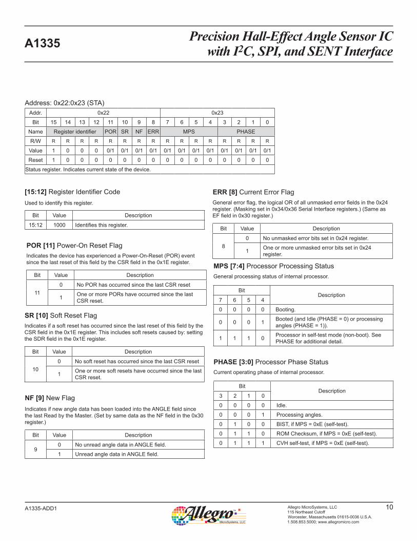
Address: 0x22:0x23 (STA)Addr. 0x22 0x23
Bit 15 14 13 12 11 10 9 8 7 6 5 4 3 2 1 0
Name Register identifier POR SR NF ERR MPS PHASE
R/W R R R R R R R R R R R R R R R R
Value 1 0 0 0 0/1 0/1 0/1 0/1 0/1 0/1 0/1 0/1 0/1 0/1 0/1 0/1
Reset 1 0 0 0 0 0 0 0 0 0 0 0 0 0 0 0
Status register. Indicates current state of the device.
[15:12] Register Identifier CodeUsed to identify this register.
Bit Value Description
15:12 1000 Identifies this register.
POR [11] Power-On Reset FlagIndicates the device has experienced a Power-On-Reset (POR) event since the last reset of this field by the CSR field in the 0x1E register.
Bit Value Description
110 No POR has occurred since the last CSR reset
1 One or more PORs have occurred since the last CSR reset.
SR [10] Soft Reset FlagIndicates if a soft reset has occurred since the last reset of this field by the CSR field in the 0x1E register. This includes soft resets caused by: setting the SDR field in the 0x1E register.
Bit Value Description
100 No soft reset has occurred since the last CSR reset
1 One or more soft resets have occurred since the last CSR reset.
NF [9] New FlagIndicates if new angle data has been loaded into the ANGLE field since the last Read by the Master. (Set by same data as the NF field in the 0x30 register.)
Bit Value Description
90 No unread angle data in ANGLE field.
1 Unread angle data in ANGLE field.
ERR [8] Current Error FlagGeneral error flag, the logical OR of all unmasked error fields in the 0x24 register. (Masking set in 0x34/0x36 Serial Interface registers.) (Same as EF field in 0x30 register.)
Bit Value Description
80 No unmasked error bits set in 0x24 register.
1 One or more unmasked error bits set in 0x24 register.
MPS [7:4] Processor Processing StatusGeneral processing status of internal processor.
BitDescription
7 6 5 4
0 0 0 0 Booting.
0 0 0 1 Booted (and Idle (PHASE = 0) or processing angles (PHASE = 1)).
1 1 1 0 Processor in self-test mode (non-boot). See PHASE for additional detail.
PHASE [3:0] Processor Phase StatusCurrent operating phase of internal processor.
BitDescription
3 2 1 0
0 0 0 0 Idle.
0 0 0 1 Processing angles.
0 1 0 0 BIST, if MPS = 0xE (self-test).
0 1 1 0 ROM Checksum, if MPS = 0xE (self-test).
0 1 1 1 CVH self-test, if MPS = 0xE (self-test).

Precision Hall-Effect Angle Sensor ICwith I2C, SPI, and SENT InterfaceA1335
11Allegro MicroSystems, LLC115 Northeast CutoffWorcester, Massachusetts 01615-0036 U.S.A.1.508.853.5000; www.allegromicro.com
A1335-ADD1
Address: 0x24:0x25 (ERR)Addr. 0x24 0x25
Bit 15 14 13 12 11 10 9 8 7 6 5 4 3 2 1 0
Name Register identifier XER XOV IER CRC NR AT AH AL OV UV MH ML
R/W R R R R R R – – – R R R R R R R
Value 1 0 1 0 0/1 0/1 X X X 0/1 0/1 0/1 0/1 0/1 0/1 0/1
Reset 1 0 1 0 0 0 0 0 0 0 0 0 0 0 0 0
Error register. Indicate various current error conditions. When set, can only be cleared via the 0x1E register CER field, hard reset (HDR field), or power-on reset. Can be masked by 0x34 register or EMSK setting in EEPROM (see XER field descriptions for masking exceptions).
Continued on the next page…
XER [11] Extended Error FlagGeneral error flag, the logical OR of all unmasked error fields in the 0x26 register. (Not masked by 0x36 Serial Interface register field.) In order to fully mask the XER flag, each bit in the 0x26 register must be individually masked.
Bit Value Description
110 No unmasked error fields set in the 0x26 register.
1 One or more unmasked error fields set in the 0x26 register.
XOV [10] Extended Access Overflow FlagIndicates a new access to extended address memory occurred before the previous access had completed; data may be invalid. XOV can be masked by the XO field in the 0x318 register.)
Bit Value Description
100 No overflow access detected.
1 One or more overflow accesses detected.
AT [6] Angle Processing Error FlagIndicates the front end is no longer acquiring angles at the correct rate. This error indicates possible missing magnet conditions, misprogrammed EEPROM, or a combination of extreme rotation speed with low refresh rate settings.
Bit Value Description
60 No error detected.
1 An angle acquisition time out has occurred.
AH [5] Angle High Fault FlagIndicates a target angle greater than the angle set in the MAX_ANGLE field has been detected.
Bit Value Description
50 No excessive angle detected.
1 Excessive angle detected.
[15:12] Register Identifier CodeUsed to identify this register.
Bit Value Description
15:12 1010 Identifies this register.
IER [9] Interface ErrorInvalid number of bits in SPI packet, or bit 15 of MOSI data = ‘1’. Packet was discarded. Will also be asserted during a Manchester or SENT communication error.
Bit Value Description
90 No error detected.
1 SPI interface error detected.
CRC [8] CRC ErrorIncoming SPI CRC error. Packet was discarded.
Bit Value Description
80 No error detected.
1 SPI CRC error detected.
NR [7] Not in Run modeSet if the processor is not actively processing angle data (no angle register updates).
Bit Value Description
70 Processor in Run mode.
1 Processor not in Run mode (angle data not being refreshed).

Precision Hall-Effect Angle Sensor ICwith I2C, SPI, and SENT InterfaceA1335
12Allegro MicroSystems, LLC115 Northeast CutoffWorcester, Massachusetts 01615-0036 U.S.A.1.508.853.5000; www.allegromicro.com
A1335-ADD1
ML [0] Magnetic Sense Low Fault Flag
Indicates detected magnetic field flux density (B) relative to MAG_LOW.
Bit Value Description
00 Magnetic flux density greater than MAG_LOW
detected.
1 Magnetic flux density less than MAG_LOW detected.
MH [1] Magnetic Sense High Fault Flag
Indicates detected magnetic field flux density (B) relative to MAG_HIGH.
Bit Value Description
10 Magnetic flux density less than MAG_HIGH
detected.
1 Magnetic flux density greater than MAG_HIGH detected.
AL [4] Angle Low Fault Flag
Indicates a target angle smaller than the angle set in the MIN_ANGLE field has been detected.
Bit Value Description
40 No excessively small angle detected.
1 Excessively small angle detected.
UV [2] Undervoltage Fault FlagIndicates a supply undervoltage has been detected.
Bit Value Description
20 No VCC undervoltage detected.
1 VCC undervoltage detected.
OV [3] Overvoltage Fault FlagIndicates a supply overvoltage condition has been detected. During normal EEPROM programming, the high-voltage EEPROM programming pulses trigger this bit.
Bit Value Description
30 No VCC overvoltage detected.
1 VCC overvoltage detected.

Precision Hall-Effect Angle Sensor ICwith I2C, SPI, and SENT InterfaceA1335
13Allegro MicroSystems, LLC115 Northeast CutoffWorcester, Massachusetts 01615-0036 U.S.A.1.508.853.5000; www.allegromicro.com
A1335-ADD1
Address: 0x26:0x27 (XERR)Addr. 0x26 0x27
Bit 15 14 13 12 11 10 9 8 7 6 5 4 3 2 1 0
Name Register identifier SS ES AW TR SU EU WC WT RC XE ME ST
R/W R R R R R R R R R R R R R R R R
Value 1 0 1 1 0/1 0/1 X X 0/1 0/1 0/1 0/1 X X 0/1 0/1
Reset 1 0 1 1 0 0 0 0 0 0 0 0 0 0 0 0
Extended Error register. Indicate various current error conditions. When set, can only be cleared via the 0x1E register CXE field, power-on reset, or hard reset. Can be masked by 0x36 register.
[15:12] Register Identifier CodeUsed to identify this register.
Bit Value Description
15:12 1011 Identifies this register.
SS [11] SRAM Soft Error FlagIndicates a correctable error in internal SRAM has been detected.
Bit Value Description
110 No SRAM soft error detected.
1 One or more SRAM soft errors detected.
ES [10] EEPROM Soft Error FlagIndicates a correctable error in internal EEPROM has been detected.
Bit Value Description
100 No EEPROM soft error detected.
1 One or more EEPROM soft errors detected.
AW [9] Angle WarningIndicates there is a warning condition present in the Angle Status register. The Angle Status register can be read using extended read command 0xFFFC.
Bit Value Description
80 No warnings.
1 One or more warnings have occurred.
TR [8] Temperature Sensor Error FlagIndicates a that the temperature sensor has detected a temperature outside of extreme limits (–50°C to 175°C).
Bit Value Description
80 No out of bounds temperature detected.
1 Out of bounds temperature detected.
SU [7] SRAM Hard Error FlagIndicates an uncorrectable error in internal SRAM has been detected.
Bit Value Description
70 No SRAM hard error detected.
1 One or more SRAM hard errors detected.
EU [6] EEPROM Hard Error Flag
Indicates an uncorrectable error in internal EEPROM has been detected.
Bit Value Description
60 No EEPROM hard error detected.
1 One or more EEPROM hard errors detected.
WC [5] Watchdog Processor Halted Fault Flag
Indicates the processor halted.
Bit Value Description
50 Processor has not halted.
1 Processor halt detected.
WT [4] Watchdog Timer Fault FlagIndicates a processor timeout has occurred (processor may be inactive).
Bit Value Description
40 No timeout detected.
1 Timeout detected.
Continued on the next page…

Precision Hall-Effect Angle Sensor ICwith I2C, SPI, and SENT InterfaceA1335
14Allegro MicroSystems, LLC115 Northeast CutoffWorcester, Massachusetts 01615-0036 U.S.A.1.508.853.5000; www.allegromicro.com
A1335-ADD1
ST [0] Self-Test Failure FlagIndicates a Boot-time or other self-test failure has been detected. Obtain STStatus value by reading Extended Access address 0xFFFC.
Bit Value Description
00 No self-test failure detected.
1 Self-test failure detected.
ME [1] Memory Address Error FlagInvalid address range on extended address access detected. This includes access to a valid location, such as EEPROM, if the Customer Access Code had not set before attempting a write.
Bit Value Description
10 No memory address issue detected.
1 Memory address issue detected.
XE [2] Execution Error FlagIndicates a requested extended operation has failed to execute correctly. For example, if a signal error is detected during an EEPROM write, this flag would be asserted.
Bit Value Description
20 No execution error detected.
1 Execution error detected.
Address: 0x26:0x27 (XERR) (continued)
RC [3] Reset Condition FlagIndicates the A1335 has been reset or powered-up. This includes power-on reset, so RC will always assert on power-up. Obtain ResetStatus value by reading Extended Access address 0xFFFC.
Bit Value Description
30 No reset has occurred since this bit was last
cleared.
1 Reset has occurred one or more times since this bit was last cleared.

Precision Hall-Effect Angle Sensor ICwith I2C, SPI, and SENT InterfaceA1335
15Allegro MicroSystems, LLC115 Northeast CutoffWorcester, Massachusetts 01615-0036 U.S.A.1.508.853.5000; www.allegromicro.com
A1335-ADD1
Address: 0x28:0x29 (TSEN)Addr. 0x28 0x29
Bit 15 14 13 12 11 10 9 8 7 6 5 4 3 2 1 0
Name Register identifier TEMPERATURE
R/W R R R R R R R R R R R R R R R R
Value 1 1 1 1 0/1 0/1 0/1 0/1 0/1 0/1 0/1 0/1 0/1 0/1 0/1 0/1
Reset 1 1 1 1 0 0 0 0 0 0 0 0 0 0 0 0
Temperature Sensor register. Stores the most recent device temperature reading generated and updated automatically by the device processor.
[15:12] Register Identifier CodeUsed to identify this register.
Bit Value Description
15:12 1111 Identifies this register.
TEMPERATURE [11:0] Device Internal TemperatureThe device internal temperature is monitored by the device internal processor and the updated value is written to this register on a periodic basis. The encoded value in this field, n, is converted as n × 1/8 = Kelvin. Example: 1010 1010 1011 (0xAAB) represents 2731 / 8 decimal, or 341.375 K (approximately 68.23°C).
Bit Value Description
11:0 0/1 Encoded Kelvin temperature.
Address: 0x2A:0x2B (FIELD)Addr. 0x2A 0x2B
Bit 15 14 13 12 11 10 9 8 7 6 5 4 3 2 1 0
Name Register identifier Magnetic Field Strength
R/W R R R R R R R R R R R R R R R R
Value 1 1 1 0 0/1 0/1 0/1 0/1 0/1 0/1 0/1 0/1 0/1 0/1 0/1 0/1
Reset 1 1 1 0 0 0 0 0 0 0 0 0 0 0 0 0
Magnetic field storage. Stores the most recent magnetic field reading generated and updated automatically by the device processor in gauss.
[15:12] Register Identifier CodeUsed to identify this register.
Bit Value Description
15:12 1110 Identifies this register.
Magnetic Field Strength [11:0]The absolute magnitude of the magnetic field is calculated by the device on a periodic basis. The value is stored in gauss. Thus 0001 0010 1100 (0x12C) represents 300 G.
Bit Value Description
11:0 0/1 Magnetic field data in gauss.

Precision Hall-Effect Angle Sensor ICwith I2C, SPI, and SENT InterfaceA1335
16Allegro MicroSystems, LLC115 Northeast CutoffWorcester, Massachusetts 01615-0036 U.S.A.1.508.853.5000; www.allegromicro.com
A1335-ADD1
Address: 0x34:0x35 (ERM)Addr. 0x34 0x35
Bit 15 14 13 12 11 10 9 8 7 6 5 4 3 2 1 0
Name Register identifier – XOV IER CRC NR AT AH AL OV UV MH ML
R/W R R R R – R/W – – – R/W R/W R/W R/W R/W R/W R/W
Value 1 1 0 0 X 0/1 X X X 0/1 0/1 0/1 0/1 0/1 0/1 0/1
Reset 1 1 0 0 0 0 0 0 0 0 0 0 0 0 0 0
Error Register Mask register. Fields used to mask corresponding bitfields (bitfield numbers match) in the 0x24 register from asserting the main Error flag. Set individual fields to 1 to prevent (mask) the corresponding 0x24 register field from affecting the global Error flags (EF in the 0x30 register and 0x24 in the 0x22 register). Values loaded from EEPROM, EMSK field at power-up or hard reset (HDR field). Bits 15:12 are used to identify the register and are fixed at 1100.
Address: 0x36:0x37 (XERM)Addr. 0x36 0x37
Bit 15 14 13 12 11 10 9 8 7 6 5 4 3 2 1 0
Name Register identifier SS ES AW TR SU EU WC WT RC XE ME ST
R/W R R R R R/W R/W R/W R/W R/W R/W R/W R/W R/W R/W R/W R/W
Value 1 1 0 1 0/1 0/1 0/1 0/1 0/1 0/1 0/1 0/1 0/1 0/1 0/1 0/1
Reset 1 1 0 1 0 0 0 0 0 0 0 0 0 0 0 0
Extended Error Register Mask register. Fields used to mask corresponding bitfields (bitfield numbers match) in the 0x26 register from asserting the 0x26 Error flag. Set individual fields to 1 to prevent (mask) the corresponding 0x26 register field from affecting the global Error flags (EF in the 0x30 register, and 0x24 in the 0x22 register) by ORing with the XER field in the 0x24 register. Values loaded from EEPROM, EMSK field at power-up or hard reset (HDR field). Bits 15:12 are used to identify the register and are fixed at 1101.

Precision Hall-Effect Angle Sensor ICwith I2C, SPI, and SENT InterfaceA1335
17Allegro MicroSystems, LLC115 Northeast CutoffWorcester, Massachusetts 01615-0036 U.S.A.1.508.853.5000; www.allegromicro.com
A1335-ADD1
I2C Interface DescriptionI2C is a serial interface that uses two bus lines, SCL and SDA, to access the internal device registers. Data is exchanged between a Master controller (for example, a microcontroller) and the A1335, the Slave. The Master can directly read and write the Primary Serial Interface registers (see Table 2). These registers are acces-sible without involving the A1335 processor, so are accessible with no additional latency. Extended addressing also is available, giving access to data through processor controlled code.
The clock input to SCL is generated by the Master, while the SDA line functions as either an input or an open drain output, depending on the direction of the data transfer. I2C timing is sum-marized in Figure 2.
I2C communication is composed of several steps in the following sequence:
1. Start Condition. Defined by a negative edge on the SDA line, while SCL is high.
2. Address Cycle. 7 device (Slave) Address bits, plus 1 bit to indicate write (0) or read (1), followed by an Acknowledge bit.
3. Data Cycles. Reading or writing 8 data bits, followed by an Acknowledge bit. This cycle can be repeated for multiple bytes of data transfer. The first data byte on a write could be the register address. See the following sections for further information.
4. Stop Condition. Defined by a positive edge on the SDA line, while SCL is high.
Except to indicate a Start or Stop condition, SDA must be stable while SCL is high. SDA can only be changed while SCL is low for data bits.
It is possible for the Start or Stop condition to occur at any time
during a data transfer. The A1335 always responds by resetting the data transfer sequence.
The state of the Read/Write bit is set low to indicate a Write cycle and set high to indicate a Read cycle.
The Master monitors for an Acknowledge bit to determine if the Slave device is responding to the address byte sent to the A1335. When the A1335 decodes the 7-bit address field as a valid address, it responds by pulling SDA low during the ninth clock cycle.
During a data write from the Master, the A1335 pulls SDA low during the clock cycle that follows the data byte, in order to indi-cate that the data has been successfully received.
After sending either an address byte or a data byte, the Master device must release the SDA line before the ninth clock cycle, in order to allow the handshaking to occur.
The default slave address for the A1335 is 00011xx, where the two LSB bits are set by the package pins (SA1 and SA0) being tied high or low. This selects one of four unique hardware addresses, as follows:
Default I2C Slave Addresses
Pin Connection Address ValueSA1 [A1] SA0[A0]
BYP BYP 00011 11
BYP GND 00011 10
GND BYP 00011 01
GND GND 00011 00
Refer to the INTF field (0x319) in the EEPROM Description and Programming section for alternative, programmatic settings.
The I2C is a byte-oriented protocol. The communication inter
Figure 2: I2C input and output timing
SDA
SCL
tSU(STA) tHD(STA) tSU(DAT) tHD(DAT) tBUF tSU(STO)
tHIGH tLOW
Precision Hall-Effect Angle Sensor ICwith I2C, SPI, and SENT InterfaceA1335
18Allegro MicroSystems, LLC115 Northeast CutoffWorcester, Massachusetts 01615-0036 U.S.A.1.508.853.5000; www.allegromicro.com
A1335-ADD1
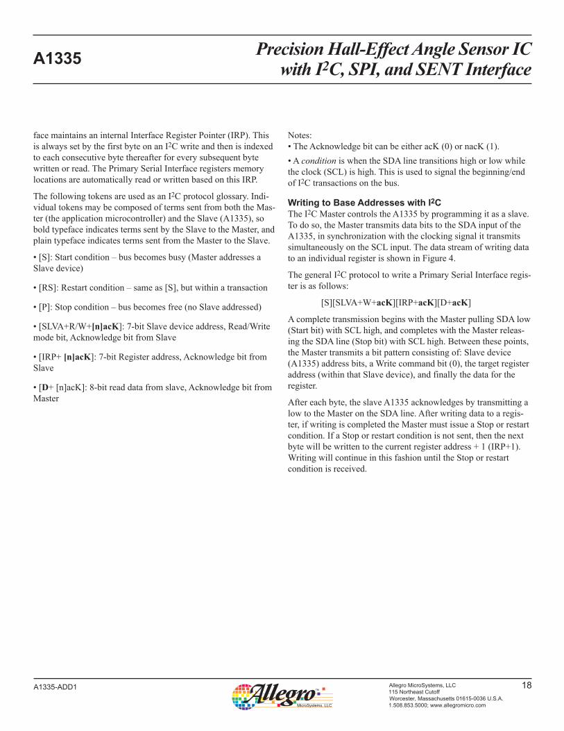
face maintains an internal Interface Register Pointer (IRP). This is always set by the first byte on an I2C write and then is indexed to each consecutive byte thereafter for every subsequent byte written or read. The Primary Serial Interface registers memory locations are automatically read or written based on this IRP.
The following tokens are used as an I2C protocol glossary. Indi-vidual tokens may be composed of terms sent from both the Mas-ter (the application microcontroller) and the Slave (A1335), so bold typeface indicates terms sent by the Slave to the Master, and plain typeface indicates terms sent from the Master to the Slave.
• [S]: Start condition – bus becomes busy (Master addresses a Slave device)
• [RS]: Restart condition – same as [S], but within a transaction
• [P]: Stop condition – bus becomes free (no Slave addressed)
• [SLVA+R/W+[n]acK]: 7-bit Slave device address, Read/Write mode bit, Acknowledge bit from Slave
• [IRP+ [n]acK]: 7-bit Register address, Acknowledge bit from Slave
• [D+ [n]acK]: 8-bit read data from slave, Acknowledge bit from Master
Notes: • The Acknowledge bit can be either acK (0) or nacK (1).• A condition is when the SDA line transitions high or low while the clock (SCL) is high. This is used to signal the beginning/end of I2C transactions on the bus.
Writing to Base Addresses with I2CThe I2C Master controls the A1335 by programming it as a slave. To do so, the Master transmits data bits to the SDA input of the A1335, in synchronization with the clocking signal it transmits simultaneously on the SCL input. The data stream of writing data to an individual register is shown in Figure 4.
The general I2C protocol to write a Primary Serial Interface regis-ter is as follows:
[S][SLVA+W+acK][IRP+acK][D+acK]
A complete transmission begins with the Master pulling SDA low (Start bit) with SCL high, and completes with the Master releas-ing the SDA line (Stop bit) with SCL high. Between these points, the Master transmits a bit pattern consisting of: Slave device (A1335) address bits, a Write command bit (0), the target register address (within that Slave device), and finally the data for the register.
After each byte, the slave A1335 acknowledges by transmitting a low to the Master on the SDA line. After writing data to a regis-ter, if writing is completed the Master must issue a Stop or restart condition. If a Stop or restart condition is not sent, then the next byte will be written to the current register address + 1 (IRP+1). Writing will continue in this fashion until the Stop or restart condition is received.

Precision Hall-Effect Angle Sensor ICwith I2C, SPI, and SENT InterfaceA1335
19Allegro MicroSystems, LLC115 Northeast CutoffWorcester, Massachusetts 01615-0036 U.S.A.1.508.853.5000; www.allegromicro.com
A1335-ADD1
1 2 3 4 5 6 7 8 9 1 2 3 4 5 6 7 8 9
A1A2A3A4A5A6 A0 RA7 RA6 RA5 RA4 RA3 RA2 RA1 RA0AK AK
Register AddressSlave Device Address
Start
WSDA
SCL
AK
acknowledgefrom A1335 (Slave)
acknowledgefrom A1335 (Slave)
acknowledgefrom A1335 (Slave)
1
1
2 3 4 5 6 7 8 9
Data (MSB byte)
acknowledgefrom A1335 (Slave)
Data (LSB byte)
D14 D13 D12 D11 D10 D9 D8
AK
Stop
2 3 4 5 6 7 8 9
D6 D5 D4 D3 D2 D1 D0
D15
D7
0 3
0 0 0 0 0 0 0 0 0
0
1 1
3
0 0 1 1
0 0 1 1
4
0 1 0 0
0
0 0 0 0
2
0 0 1 0
3 5
10 0 1
SDA
(Write) (Write)
Write to
PrimaryRegister
PrimaryRegister
Read from
SCL
Slave Address+ W bit
Slave Address+ W bit
Slave Address+ R bit
Load RegisterAddress
Load RegisterAddress
(Write)
Load TargetData
Restart Read Data
(Write) (Write) (Write)
SDA
SCL
(Read) (Read)
. . .
. . . . . . . . . . . .
. . .
Figure 3: I2C Base Address Write and Read Sessions Examples.High-voltage pulses are required on VCC only to invoke an EEPROM write.
Figure 4: I2C Base Address Write: value 0x0235 to register address 0x34 (ERM) in slave device 0x3. All steps must occur immediately after the first step, with no intervening transmissions.

Precision Hall-Effect Angle Sensor ICwith I2C, SPI, and SENT InterfaceA1335
20Allegro MicroSystems, LLC115 Northeast CutoffWorcester, Massachusetts 01615-0036 U.S.A.1.508.853.5000; www.allegromicro.com
A1335-ADD1
Figure 5: I2C Base Address Read: angle value and error status from register address 0x20 (ANG) in slave device 0x3. All steps must occur immediately after the first step, with no intervening transmissions.
Register AddressSlave Device Address
W
acknowledgefrom A1335 (Slave)
acknowledgefrom A1335 (Slave)
Data (MSB byte)
1 2 3 4 5 6 7 8 9 1 2 3 4 5 6 7 8 9
A1A2A3A4A5A6 A0 AK AK
Start
SDA
SCL
acknowledgefrom Master
Data (LSB byte)
acknowledgefrom Master
Stop
1 2 3 4 5 6 7 8 9
NAKD6 D5 D4 D3 D2 D1 D0D7
RA7 RA6 RA5 RA4 RA3 RA2 RA1 RA0
Slave Device Address
acknowledgefrom A1335 (Slave)
1 2 3 4 5 6 7 8 9 1 2 3 4 5 6 7 8 9
A1A2A3A4A5A6 A0 AK AK
Restart
SDA
SCL
SDA
SCL
EF NF P D11 D10 D9 D8R
0 3
0 0 0 0 0 1 1
2
000 0 1
0
00 0 0 0 0
0 3
0 0 0 0 0 1 1
0xn
0/1 0/1 0/1 0/1 0/1 0/1 0/1 0/1
0
01 0
0xn
0xn
0/1 0/1 0/1 0/1 0/1 0/1 0/1 0/1 1
0xn
Reading from Base Addresses using I2CWhen the Master performs a data read from an A1335 internal register, a combined data transmission format is used. The I2C Master provides the Start bit, the A1335 device (slave) address, the read/write bit set to Write (0), and then the initial source regis-ter address. The Master initially does a write to set the IRP.
The Master then issues another Start bit (referred to as Restart) followed by the same slave address and the read/write bit set to Read (1). The A1335 then provides data read-out, one byte at a time. The data stream of reading data from an individual register is shown in Figure 5.
The general I2C protocol to read a Primary Serial Interface regis-ter is as follows:
1. [S][SLVA+W+acK][IRP+acK] 2. [RS][SLVA+R+acK][DATA@IRP+acK] [(DATA@IRP+1)+nacK][P]
After each byte except for the last, the Master acknowledges by transmitting a low to the slave A1335 on the SDA line. If reading is completed, then the Master must issue a nacK, and then either
a stop or a restart. As long as the Master continues to acK each reading, the IRP will be advanced, and the A1335 will continue to transmit the contents of the subsequent registers.
I2C Data Redundancy ModeA data redundancy mode can be set via the EEPROM register INTF (0x319) DR bit (bit 11). In this mode, on I2C reads, every other byte is the 1’s Complement of the previous byte. For instance, when reading the ANG register:1. [S][SLVA+W+acK][0x20+acK]2. [RS][SLVA+R+acK][ANG[15:8]+K][~ANG[15:8]+K]
[ANG[7:0]+K][~ANG[7:0]+nacK] [P]If the ERD register (addresses 0x0E:0x11) were read:1. [S][SLVA+W+acK][0x04+acK]2. [RS][SLVA+R+acK][EDAT[31:24]+acK]
[~EDAT[31:24]+acK][EDAT[23:16]+acK][~EDAT[23:16]+acK][EDAT[15:8]+K][~EDAT[15:8]+acK][EDAT[7:0]+acK][~EDAT[7:0]+nacK][P]
The complement pattern is restarted at the beginning of any I2C transaction (after a Start or Restart), so the first byte read is always the “real” data and the next byte the complemented data.

Precision Hall-Effect Angle Sensor ICwith I2C, SPI, and SENT InterfaceA1335
21Allegro MicroSystems, LLC115 Northeast CutoffWorcester, Massachusetts 01615-0036 U.S.A.1.508.853.5000; www.allegromicro.com
A1335-ADD1
SPI InterfaceThe A1335 provides a full-duplex 4-pin SPI interface for each die utilizing SPI mode 3. The sensor responds to commands received on the corresponding MOSI (Master-Out Slave-In), SCLK (Serial Clock), and CS (Chip Select) pins, and outputs data on the MISO (Master-In Slave-Out) pin. The SPI pins double as I2C data, clock, and address lines. A separate ISEL (Interface Select) pin is used to select between the two communication protocols. SPI is selected when ISEL is brought to a logic high. This is easily accomplished by tying the ISEL pin directly to the BYP pin of the A1335, which provides a constant ≈2.8 V.
SPI Interface Timing
The SPI interface operates in pure Slave mode, with the Mas-ter controlling the SCLK, MOSI, and CS lines. The Master can maximize data throughput, up to fSCLK(max) of 10 MHz.
Figure 6 shows the timings of the Write and Read cycles.
Figure 6: A1335 SPI Interface Timings: (upper) input and (lower) output
Input to A1335 CSx
SCLKx
MOSIx
CSx
SCLKx
MISOx
Output from A1335
≥ tCS
tCS
tSU tHD
tCHDtSCLKL tSCLKH
R / W
DO-15 DO-14
Register Contents
DO-x
≥ tCS
tCS tCHDtSCLKL
tDAV
tSCLKH

Precision Hall-Effect Angle Sensor ICwith I2C, SPI, and SENT InterfaceA1335
22Allegro MicroSystems, LLC115 Northeast CutoffWorcester, Massachusetts 01615-0036 U.S.A.1.508.853.5000; www.allegromicro.com
A1335-ADD1
SPI Message Frame Size
A SPI transaction is a minimum of 16 bits in length. An extended 20-bit SPI packet allows 4 bits of CRC to accompany every data packet. The 4-bit CRC is automatically generated and placed on the MISO line once a 17th SCLK edge is detected by the A1335. The incoming CRC on the MOSI line is ignored unless the SC bit is set within EEPROM (0x319 bit 20). When enabled, a SPI packet with an incorrect CRC will be discarded, and the CRC error flag set (bit 8 within Serial register 0x24:0x25).
CSN
SCLK
MOSI
MISO
SCLK
MOSI
MISO
CSN
0 W-1 R-0 A5 A4 A3 A2 A1 A0 DI-7 DI-6 DI-5 DI-4 DI-3 DI-2 DI-1 DI-0
DO-15 DO-14 DO-13 DO-12 DO-11 DO-10 DO-9 DO-8 DO-7 DO-6 DO-5 DO-4 DO-3 DO-2 DO-1 DO-0
0 W-1 R-0 A5 A4 A3 A2 A1 A0 DI-7 DI-6 DI-5 DI-4 DI-3 DI-2 DI-1 DI-0
DO-15 DO-14 DO-13 DO-12 DO-11 DO-10 DO-9 DO-8 DO-7 DO-6 DO-5 DO-4 DO-3 DO-2 DO-1 DO-0 OCRC-3 OCRC-2 OCRC-1 OCRC-0
ICRC-3 ICRC-2 ICRC-1 ICRC-0
Figure 7: Sixteen Bit SPI Transaction
Figure 8: Twenty Bit SPI Transaction

Precision Hall-Effect Angle Sensor ICwith I2C, SPI, and SENT InterfaceA1335
23Allegro MicroSystems, LLC115 Northeast CutoffWorcester, Massachusetts 01615-0036 U.S.A.1.508.853.5000; www.allegromicro.com
A1335-ADD1
Write Cycle OverviewWrite cycles consist of a 1-bit sync (low), a 1-bit R/W asserted high, 6 address bits (corresponding to the primary serial regis-ter), 8 data bits, and 4 optional CRC bits. To write a full 16 bit serial register, two Write commands are required (even and odd byte addresses). MOSI bits are clocked in on the rising edge of the Master-generated SCLK signal. The complete SPI packet is latched on the rising edge of the Master-generated (CS) signal.The simultaneous MISO signal output represents the contents of the corresponding die SPI read packet. Including 16 data bits and 4 optional CRC bits, automatically included if a 17th SCLK edge is detected. The data bits correspond to the register contents selected during the previous read command. In the case where no previous read command was issued, the MISO line will transmit all zeros.Read Cycle OverviewRead cycles have two stages: a Read command, selecting a serial register address, followed by another Read command to transmit the data from the selected register. Both commands consist of a 1-bit sync (low), a 1-bit R/W asserted low, 6 address bits identify-ing the target register, and 8 data bits (all zeros because no data is being written).In the first stage, as with the Write command, Read command
MOSI bits are clocked-in on the rising edge of the Master gener-ated SCLK signal, and data latched on the rising edge of the (CS) signal. During the first Read stage, the simultaneous MISO signal output is the contents of the SPI read data from the previous Read command cycle.In the second stage, the Read command continues on the next falling edge of the Master-generated (CS) signal. The MISO bits are the contents of the register selected during the first stage, read 16 bits at a time. The MISO bits transmit on the falling edges of the SCLK signal, such that the Master can sample them on the SCLK rising edges.Because a SPI Read command can transmit 16 data bits at one time, and the primary serial registers are built from one even and one odd byte, the entire 16-bit contents of one serial register may be transmitted with one SPI frame (See Table 3 for Serial Register format). This is accomplished by providing an even serial address value. If an odd value address is sent, only the contents of the single byte will be returned, with the eight most significant bits within the SPI packet set to zero.Example: To read all 16 bits of the Error register (0x24:0x25), a SPI read request using address 0x24 should be sent. If only the 8 LSBs are desired, the address 0x25 should be used. Figure 9 shows examples of both a SPI write and a SPI read request, using a 16-bit SPI message frame.
CSx
SCLKx
MOSIx
MISOx
A5 A4 A3 A2 A1 A0 D7 D6 D5 D4 D3 D2 D1 D0
A5 A4 A3 A2 A1 A0 D7 D6 D5 D4 D3 D2 D1 D0
SCLKx
MOSIx
MISOx
R/W
Inputlatched
Inputlatched
1 2 3 4 5 6 7 8 9 10 11 12 13 14 15 16
1 2 3 4 5 6 7 8 9 10 11 12 13 14 15 16
1 2 3 4 5 6 7 8 9 10 11 12 13 14 15 16
CSx
CSx
SCLKx
MOSIx
MISOx
R / W
R / W
A5 A4 A3 A2 A1 A0 D7 D6 D5 D4 D3 D2 D1 D0
Register Contents (previous Read command selection, or Don’t Care)
Register Contents (previous Read command selection, or Don’t Care)
Register Contents (previous Read command selection, or Don’t Care)
DO-15 DO-14 DO-13 DO-12 DO-11 DO-9 DO-8 DO-7 DO-6 DO-5 DO-4 DO-3 DO-2 DO-1 DO-0DO-10
DO-15 DO-14 DO-13 DO-12 DO-11 DO-9 DO-8 DO-7 DO-6 DO-5 DO-4 DO-3 DO-2 DO-1 DO-0DO-10
DO-15 DO-14 DO-13 DO-12 DO-11 DO-9 DO-8 DO-7 DO-6 DO-5 DO-4 DO-3 DO-2 DO-1 DO-0DO-10
Figure 9: SPI Read and Write Pulse Sequences
(A) SPI Write example(duplexed read available)
(B) SPI Read example:register selection(duplexed read available)
(C) SPI Read example: data output from selected register

Precision Hall-Effect Angle Sensor ICwith I2C, SPI, and SENT InterfaceA1335
24Allegro MicroSystems, LLC115 Northeast CutoffWorcester, Massachusetts 01615-0036 U.S.A.1.508.853.5000; www.allegromicro.com
A1335-ADD1
MANCHESTER SERIAL INTERFACE
To facilitate addressable device programming when using the unidirectional SENT output mode with no need for additional wiring, the A1335 incorporates a serial interface on the VCC line. (Note: The A1335 may be programmed via the SPI or I2C inter-faces, with additional wiring connections). This interface allows an external controller to read and write registers in the A1335 EEPROM and volatile memory. The device uses a point-to-point communication protocol, based on Manchester encoding per G.E. Thomas (a rising edge indicates a 0 and a falling edge indicates a 1), with address and data transmitted MSB first. The addressable Manchester code implementation uses the logic states of the SA0/SA1 pins to set address values for each die. In this way, individ-ual communication with up to four A1335 die is possible.
To prevent any undesired programming of the A1335, the serial interface can be disabled by setting the Disable Manchester bit (0x30B bit 23) to a 1. With this bit set, the A1335 will ignore any Manchester input on VCC.
Entering Manchester Communication ModeProvided the Disable Manchester bit is not set in EEPROM, the A1335 continuously monitors the VCC line for valid Manchester commands. The part takes no action until a valid Manchester Access Code is received.
There are two special Manchester code commands used to activate or deactivate the serial interface and specify the output format used during Read operations:
1. Manchester Access Code: Enters Manchester Communica-tion Mode; Manchester code output on the SENT pin.
2. Manchester Exit Code; returns the SENT pin to normal (angle data) output format.
Once the Manchester Communication Mode is entered, the SENT output pin will cease providing angle data, interrupting any data transmission in progress.
Transaction TypesAs shown in Figure 10, the A1335 receives all commands via the VCC pin, and responds to Read commands via the SENT pin.This implementation of Manchester encoding requires the com-munication pulses be within a high (VMAN(H)) and low (VMAN(L)) range of voltages on the VCC line. Writing to EEPROM is sup-ported by two high voltage pulses on the VCC line.
Each transaction is initiated by a command from the controller; the A1335 does not initiate any transactions. Two commands are recognized by the A1335: Write and Read.
Figure 10: Top-Level Programming Interface
A1335
ECU
GND
Read Manchester Code
Write/Read Command -
Manchester Code
VCC
SENT
Table 4: EEPROM Value for Serial Communication Address Bits Parameter Name Description
0x30B 23 Disable Manchester (DM) When set (logic 1) the A1335 ignores any Manchester input on the VCC line

Precision Hall-Effect Angle Sensor ICwith I2C, SPI, and SENT InterfaceA1335
25Allegro MicroSystems, LLC115 Northeast CutoffWorcester, Massachusetts 01615-0036 U.S.A.1.508.853.5000; www.allegromicro.com
A1335-ADD1
A Read command with the desired register number is sent from the controller to the A1335. The device responds with a Read Response frame using the Manchester protocol.
In addition to the contents of the requested memory location, a Return Status field is included with every Read Response. This field provides the ID used to communicate with the part and any errors which may have occurred during the transaction. These bits are:
• ID – ID (SA1/SA) unless BC = 1 (ID will be 00)
• BC – Broadcast; ID field was zero or SPI mode active
• AE – Abort Error; edge detection failure after sync detect
• OR– Overrun Error; A new Manchester command has been received before the previous request could be completed
• CS – Checksum error; a prior command had a checksum error Table 5: Return Status Bits
Return Status Bits (5 bits)5 4 3 2 1 0
ID BC AE OR CS
The serial Manchester interface uses a cyclic redundancy check (CRC) for data-bit error checking (synchronization bits are ignored during the check).
The CRC algorithm is based on the polynomialg(x) = x3 + x + 1 ,
and the calculation is represented graphically in Figure 4.
The trailing 3 bits of a message frame comprise the CRC token. The CRC is initialized at 111.
C1C0 C2 Input Data
1x 0 1x 1 0x 2 1x 3 = x3 + x + 1
Reading Data Using Manchester Encoding Error Checking
Synchronize Return Status
MSB
0 0
Data (16 Bits) CRC
...0/10/1 0/10/1 0/1 0/10/1 0/1 0/10/1 0/1 0/1 0/1 0/1 0/1
Figure 11: Manchester Read Response
Figure 12: Manchester CRC Calculation

Precision Hall-Effect Angle Sensor ICwith I2C, SPI, and SENT InterfaceA1335
26Allegro MicroSystems, LLC115 Northeast CutoffWorcester, Massachusetts 01615-0036 U.S.A.1.508.853.5000; www.allegromicro.com
A1335-ADD1
Manchester Message StructureThe general format of a command message frame is shown in Figure 13. Note that, in the Manchester coding used, a bit value of 1 is indicated by a falling edge within the bit boundary, and a bit value of zero is indicated by a rising edge within the bit boundary.
A brief description of each bit is provided in Table 6.
Table 6: Manchester Command General Format
Bits Parameter Name Values Description
2 Synchronization 00 Used to identify the beginning of a serial interface command
1 Read/Write0 [As required] Write operation
1 [As required] Read operation
4 Chip Select 0/1 Used to select a set of target chips/die, based on ID value.
6 Address 0/1 [Read/Write] Serial address
16 Data 0/1 Requested serial register contents (Write operation only)
3 CRC 0/1 Incorrect value indicates errors
When the A1335 is operating in I2C Mode (ISEL pin set to a logic low), the Die ID value is determined by the state of the SA0 and SA1 pins.
Table 7: Pin ValuesSA1 SA0 ID Value
0 0 ID0
0 1 ID1
1 0 ID2
1 1 ID3
Using the 4 bits of the Chip Select field, die can be selected via their ID value, allowing up to four die to be individually addressed and providing for different group addressing schemes. If Chip Select is all zeros or the A1335 is operating in SPI mode (ISEL pin set to a logic high), no ID comparison will be made, allowing all A1335s to be addressed at once.
Example: If Chip Select = 1010, all die with ID3 or ID1 will be selected.
Note: If the sharing a SENT line with multiple chips/dies, reading must be done one die at a time.
Table 8: Chip SelectChip Select
ID3 ID2 ID1 ID0
Figure 13: General Format for Serial Interface Commands

Precision Hall-Effect Angle Sensor ICwith I2C, SPI, and SENT InterfaceA1335
27Allegro MicroSystems, LLC115 Northeast CutoffWorcester, Massachusetts 01615-0036 U.S.A.1.508.853.5000; www.allegromicro.com
A1335-ADD1
Manchester Interface Reference
Table 9: Manchester Interface Protocol Characteristics1
Characteristics Symbol Note Min. Typ. Max. Unit
Input/Output Signal Timing
Bit Rate Defined by the input message bit rate sent from the external controller 4 – 100 kbps
Bit Time tBITData bit pulse width at 4 kbps 243 250 257 µs
Data bit pulse width at 100 kbps 9.5 10 10.5 µs
Bit Time Error errTBIT Deviation in tBIT during one command frame –11 – +11 %
Write Delay tWRITE(E)
Required delay from the end of the second EEPROM Program pulse to the leading edge of a following command frame
VCC < 6.0 V – – –
Read Delay tSTART_READ
Delay from the trailing edge of a Read command frame to the leading edge of the Read Acknowledge frame
¼ × tbit – ¾ × tbit µs
EEPROM Programming PulseEEPROM Programming Pulse Setup Time tsPULSE(E)
Delay from last bit cell of write command to start of EEPROM programming pulse 40 – – μs
Input Signal VoltageManchester Code High Voltage VMAN(H) Applied to VCC line 7.8 – – V
Manchester Code Low Voltage VMAN(L) Applied to VCC line – – 5.7 V
Output Signal Voltage (Applied on SENT Line)
Manchester Code High Voltage VMAN(H)Minimum Rpullup = 5 kΩ 0.9 × VS – – V
Maximum Rpullup = 50 kΩ 0.7 × VS – – V
Manchester Code Low Voltage VMAN(L) 5 kΩ ≤ Rpullup ≤ 50 kΩ – – 0.1 V1 Determined by design.

Precision Hall-Effect Angle Sensor ICwith I2C, SPI, and SENT InterfaceA1335
28Allegro MicroSystems, LLC115 Northeast CutoffWorcester, Massachusetts 01615-0036 U.S.A.1.508.853.5000; www.allegromicro.com
A1335-ADD1
The following command messages can be exchanged between the device and the external controller:
• Manchester Access Code• Manchester Exit Code • Read• Read Response• Write
For EEPROM address information, refer to the EEPROM Structure section. For serial address locations, refer to the serial register map.
Table 10: Manchester Access CodeFunction Transmits the Access Code to the A1335. Enters Serial Communication mode with the desired output protocol.
Syntax Sent by the external controller on the A1335 VCC pin.
Related Commands Related command: Serial Exit Code
Pulse SequenceSynchronize
MSB
Chip Select
0 0 0
Access Code(16 bits) CRC
10/1 10/1 10/1 10/1 1 1 0/1 0/10/10/10/10/1 0/10/1 0/1. . .
OptionsAccess Codes: Manchester Access Code = 0x62D2 Selects Manchester output on the SENT pin.
Examples
The Manchester Access Code operates as a broadcast pulse, meaning the Chip Select field is inconsequential. For example, if two A1335s configured with ID0 and ID1 respectively are sharing a common VCC line, a Manchester Access Code with a Chip Select Value of 0x1 results in both sensors entering Manchester Serial Communication mode.

Precision Hall-Effect Angle Sensor ICwith I2C, SPI, and SENT InterfaceA1335
29Allegro MicroSystems, LLC115 Northeast CutoffWorcester, Massachusetts 01615-0036 U.S.A.1.508.853.5000; www.allegromicro.com
A1335-ADD1
Table 11: Manchester Exit CodeFunction Returns the A1335 to normal operation.
Syntax Sent by the external controller on the A1335 VCC pin.Manchester Exit Code = Any value other than 0x62d2
Related Commands Manchester Access Codes
Pulse SequenceSynchronize
MSB
Chip Select
0 0 0
Exit Code(16 bits) CRC
10/1 10/1 10/1 10/1 1 1 0/1 0/10/10/10/10/1 0/10/1 0/1. . .
Options None
Examples Similiar to the Manchester Access code, acts as a broadcast pulse. To exit the serial communication mode, the Exit Code can be any value besides the Access Code (such as 0x0000).
Table 12: Manchester Read
FunctionDetermines the serial address within the A1335, from which the next Read Response will transmit data.The A1335 must first receive a Manchester Access Code before responding to a read command.
Syntax Sent by the external controller on the A1335 VCC pin.
Related Commands Read Response
Pulse SequenceSynchronize
MSB
Read/Write
Chip Select
0 0 1
Serial RegisterAddress CRC
0/10/1 0/10/1 0/10/1 0/10/1 0/1 0/1 0/1 0/1 0/1
Options None
Examples

Precision Hall-Effect Angle Sensor ICwith I2C, SPI, and SENT InterfaceA1335
30Allegro MicroSystems, LLC115 Northeast CutoffWorcester, Massachusetts 01615-0036 U.S.A.1.508.853.5000; www.allegromicro.com
A1335-ADD1
Table 13: Manchester Read Response
Function Transmits to the external controller data retrieved from the A1335 serial register in response to the most recent Read command.
Syntax Sent by the A1335 on the SENT pin. Sent after a Read command.
Related Commands Read
Pulse Sequence
Read Response with Manchester output.
Synchronize
MSB
See “Return Data using Manchester Encoding” for bit definitions.Since the Manchester format will only respond to a valid Read command,the NR bit is not applicable.
BC AEID OR CS
0 0
Data (16 Bits) CRC
...0/10/1 0/10/1 0/1 0/10/1 0/1 0/10/1 0/1 0/1 0/1 0/1 0/1
Options Read from an Even address returns Even byte [15:8] and Odd byte [7:0].Read from an Odd address returns Odd byte [7:0] only. Data bits [15:8] will be zeroes.
Examples –
Table 14: Manchester WriteFunction Transmits to the A1335 data prepared by the external controller.
Syntax Sent by the external controller on the A1335 VCC pin.
Related Commands
Pulse Sequence
Synchronize
MSB MSB
Read/Write
Chip Select
0 0 0
Serial RegisterAddress
Data(16 bits) CRC
0/10/1 0/10/1 0/10/1 0/10/1 0/1 0/1 0/1 0/10/10/1 0/10/1 0/1. . .
Options Data is written to Address and Address+1 if Even address (16-bit write).If Odd address, only 8 bits are written (LSB of 16-bit data field).
Examples
Precision Hall-Effect Angle Sensor ICwith I2C, SPI, and SENT InterfaceA1335
31Allegro MicroSystems, LLC115 Northeast CutoffWorcester, Massachusetts 01615-0036 U.S.A.1.508.853.5000; www.allegromicro.com
A1335-ADD1
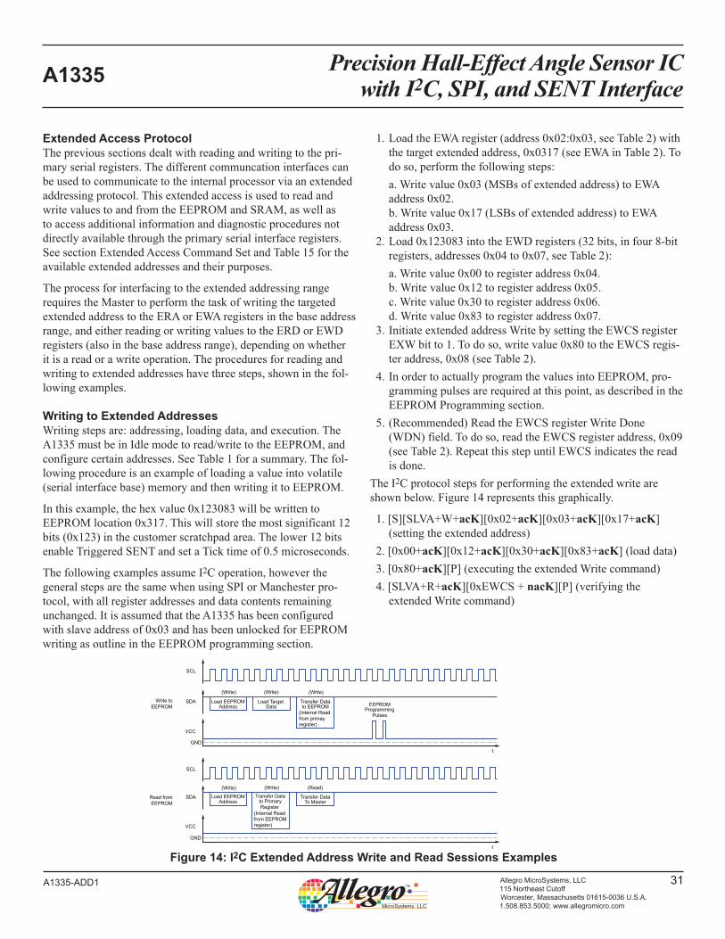
Extended Access ProtocolThe previous sections dealt with reading and writing to the pri-mary serial registers. The different communcation interfaces can be used to communicate to the internal processor via an extended addressing protocol. This extended access is used to read and write values to and from the EEPROM and SRAM, as well as to access additional information and diagnostic procedures not directly available through the primary serial interface registers. See section Extended Access Command Set and Table 15 for the available extended addresses and their purposes.
The process for interfacing to the extended addressing range requires the Master to perform the task of writing the targeted extended address to the ERA or EWA registers in the base address range, and either reading or writing values to the ERD or EWD registers (also in the base address range), depending on whether it is a read or a write operation. The procedures for reading and writing to extended addresses have three steps, shown in the fol-lowing examples.
Writing to Extended AddressesWriting steps are: addressing, loading data, and execution. The A1335 must be in Idle mode to read/write to the EEPROM, and configure certain addresses. See Table 1 for a summary. The fol-lowing procedure is an example of loading a value into volatile (serial interface base) memory and then writing it to EEPROM.
In this example, the hex value 0x123083 will be written to EEPROM location 0x317. This will store the most significant 12 bits (0x123) in the customer scratchpad area. The lower 12 bits enable Triggered SENT and set a Tick time of 0.5 microseconds.
The following examples assume I2C operation, however the general steps are the same when using SPI or Manchester pro-tocol, with all register addresses and data contents remaining unchanged. It is assumed that the A1335 has been configured with slave address of 0x03 and has been unlocked for EEPROM writing as outline in the EEPROM programming section.
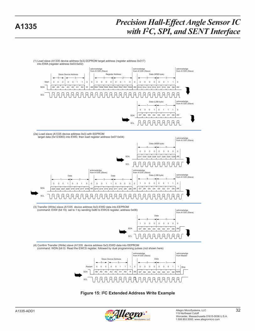
1. Load the EWA register (address 0x02:0x03, see Table 2) with the target extended address, 0x0317 (see EWA in Table 2). To do so, perform the following steps:
a. Write value 0x03 (MSBs of extended address) to EWA address 0x02.
b. Write value 0x17 (LSBs of extended address) to EWA address 0x03.
2. Load 0x123083 into the EWD registers (32 bits, in four 8-bit registers, addresses 0x04 to 0x07, see Table 2):
a. Write value 0x00 to register address 0x04. b. Write value 0x12 to register address 0x05. c. Write value 0x30 to register address 0x06. d. Write value 0x83 to register address 0x07. 3. Initiate extended address Write by setting the EWCS register
EXW bit to 1. To do so, write value 0x80 to the EWCS regis-ter address, 0x08 (see Table 2).
4. In order to actually program the values into EEPROM, pro-gramming pulses are required at this point, as described in the EEPROM Programming section.
5. (Recommended) Read the EWCS register Write Done (WDN) field. To do so, read the EWCS register address, 0x09 (see Table 2). Repeat this step until EWCS indicates the read is done.
The I2C protocol steps for performing the extended write are shown below. Figure 14 represents this graphically.
1. [S][SLVA+W+acK][0x02+acK][0x03+acK][0x17+acK] (setting the extended address)
2. [0x00+acK][0x12+acK][0x30+acK][0x83+acK] (load data)3. [0x80+acK][P] (executing the extended Write command)4. [SLVA+R+acK][0xEWCS + nacK][P] (verifying the
extended Write command)
SDA
(Write) (Write) (Write)
Write toEEPROM
Read fromEEPROM
EEPROMProgramming
Pulses
GNDt
t
SCL
VCC
VCC
Load Target Data
Load EEPROMAddress
Load EEPROMAddress
Transfer DataTo Master
(Write)
Transfer Datato EEPROM
(Internal Readfrom primayregister)
(Internal Readfrom EEPROMregister)
(Write) (Read)Transfer Data
to Primary Register
SDA
GND
SCL
Figure 14: I2C Extended Address Write and Read Sessions Examples
Precision Hall-Effect Angle Sensor ICwith I2C, SPI, and SENT InterfaceA1335
32Allegro MicroSystems, LLC115 Northeast CutoffWorcester, Massachusetts 01615-0036 U.S.A.1.508.853.5000; www.allegromicro.com
A1335-ADD1
Figure 15: I2C Extended Address Write Example
1 2 3 4 5 6 7 8 9 1 2 3 4 5 6 7 8 9
A1A2A3A4A5A6 A0 RA7 RA6 RA5 RA4 RA3 RA2 RA1 RA0AK AK
Register AddressSlave Device Address
Start
WSDA
SCL
SDA
SCL
AK
acknowledgefrom A1335 (Slave)
acknowledgefrom A1335 (Slave)
acknowledgefrom A1335 (Slave)
1
1
2 3 4 5 6 7 8 9
Data (MSB byte)
acknowledgefrom A1335 (Slave)
(1) Load slave (A1335 device address 0x3) EEPROM target address (register address 0x317)into EWA (register address 0x03:0x02)
(2a) Load slave (A1335 device address 0x3) with EEPROMtarget data (0x123083) into EWD, then load register address 0x07:0x04)
(3) Transfer (Write) slave (A1335 device address 0x3) EWD data into EEPROM(command: EXW (bit 15) set to 1 by sending 0x80 to EWCS register, address 0x08)
Data (LSB byte)
D14 D13 D12 D11 D10 D9 D8
AK
2 3 4 5 6 7 8 9
D6 D5 D4 D3 D2 D1 D0
D15
D7
9
SDA
SCL
SDA
SCL
AK
1 2 3 4 5 6 7 8 9
A1A2A3A4A5A6 A0 AK
Slave Device Address
RSDA
SCL
acknowledgefrom A1335 (Slave)
SDA
SCL
acknowledgefrom A1335 (Slave)
1
1
2 3 4 5 6 7 8 9
Data (MSB byte)
acknowledgefrom A1335 (Slave)
Data (LSB byte)
D30 D29 D28 D27 D26 D25 D24
AK
2 3 4 5 6 7 8 9
D6 D5 D4 D3 D2 D1 D0
D31
AK
acknowledgefrom A1335 (Slave)
1 2 3 4 5 6 7 8 9
Data
1 2 3 4 5 6 7 8 9
AK AK
acknowledgefrom A1335 (Slave)
acknowledgefrom A1335 (Slave)
1 2 3 4 5 6 7 8 9
DataData
D14 D13 D12 D11 D10 D9 D8D15D22 D21 D20 D19 D18 D17 D16D23 D7
D6 D5 D4 D3 D2 D1 D0D7
(4) Confirm Transfer (Write) slave (A1335 device address 0x3) EWD data into EEPROM(command: WDN (bit 0) Read the EWCS register, followed by dual programming pulses (not shown here)
NAK
acknowledgefrom Master
1 2 3 4 5 6 7 8 9
Data
D6 D5 D4 D3 D2 D1 D0D7
StopRestart
0 3
0 0 0 0 0 0 0 00 0
0
1 1
0
0 0 0 0
0 0 0 1
2
0 0 1
0
0 0 0 0
3
0 0 1 1
1 7
10 1 1
0
01 0 0 0
0 3
0 0 0 0 0 1 01 1
0
0 0 0 0
0
0 0 0 0
0
8
1 0 0 0
0
0 0 0 0
00 0
1
0 00 1
2
0 0 1
3
0 0 1 1
0
0 0 0 0
8 3
00 1 1
1
0
0 0 0 0
1
0 0 0 1

Precision Hall-Effect Angle Sensor ICwith I2C, SPI, and SENT InterfaceA1335
33Allegro MicroSystems, LLC115 Northeast CutoffWorcester, Massachusetts 01615-0036 U.S.A.1.508.853.5000; www.allegromicro.com
A1335-ADD1
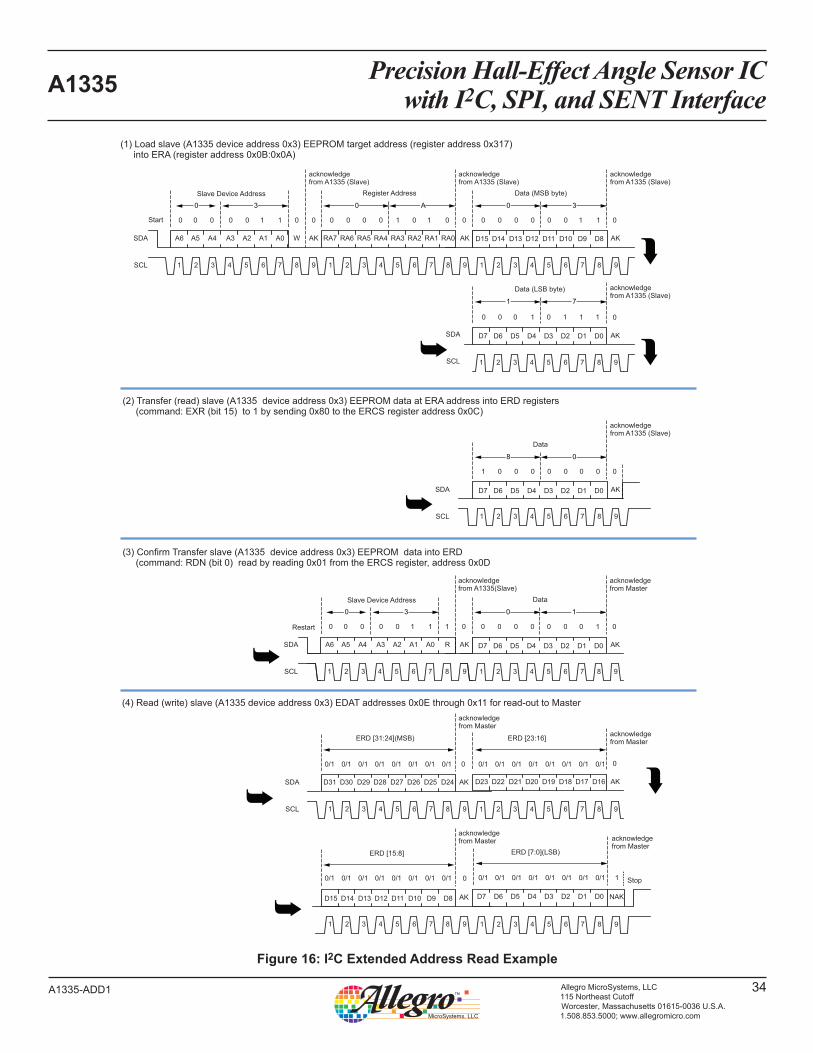
Reading from Extended Addresses Reading steps are: addressing, execution, and read-out. The following procedure is an example of loading a value from EEPROM into volatile (serial interface base) memory from which it can be accessed by the Master.
In this example, read the contents of EEPROM location 0x0317. This procedure is presented graphically in Figure 16.
1. Load the ERA register (address 0x0A:0x0B, see Table 2) with the target extended address 0x0317 (see ERA in Table 2). To do so:
a. Write value 0x03 (MSBs of extended address) to ERA address 0x0A.
b. Write value 0x17 (LSBs of extended address) to ERA address 0x0B.
2. Set extended access Read mode by setting the ERCS register EXR bit to 1. To do so, write value 0x80 to the ERCS register address, 0x0C (see Table 2).
3. Read the ERCS register Read Done (RDN) field. To do so, read the ERCS register address, 0x0D (see Table 2).
4. Read the ERD registers (32 bits, in four 8-bit registers, addresses 0x0E to 0x11, see Table 2), 16 bits at a time, 0x0E through 0x11.
The I2C protocol steps for performing the extended read are shown below. For simplicity it is assumed that the A1335 has been configured with a slave address of 0x03. Figure 16 repre-sents this graphically.
1. [S][SLVA+W+acK][0x0A+acK][0x03+acK][0x17+acK] (setting the extended address)
2. [0x80+acK] (executing the extended Read command)3. [RS][SLVA+R+acK][ERCS[7:0]+ack] (verifying the
extended Read command)4. [ERD[31:24]+acK][ERD[23:16]+acK][ERD[15:8]+acK]
[ERD[7:0]+nacK][P] (A1335 streaming ERD registers)
Table 2: Primary Serial Interface Registers (Reserved Registers Not Shown) (reproduced from page 3 for easy reference)
Address*(Hex) Name Usage
02:03 EWA Extended Write Address
04:07 EWD Extended Write Data
08:09 EWCS Extended Write Control and Status
0A:0B ERA Extended Read Address
0C:0D ERCS Extended Read Control and Status
0E:11 ERD Extended Read Data
1E:1F CTRL Device control
20:21 ANG Current angle and related data
22:23 STA Device status
24:25 ERR Device error status
26:27 XERR Extended error status
28:29 TSEN Temperature sensor data
2A:2B FIELD Magnetic field strength
34:35 ERM Device error status masking
36:37 XERM Extended error status masking
*Addresses that span multiple bytes are addressed by the most significant byte (lower address in the address range corresponds to the most significant byte).
Precision Hall-Effect Angle Sensor ICwith I2C, SPI, and SENT InterfaceA1335
34Allegro MicroSystems, LLC115 Northeast CutoffWorcester, Massachusetts 01615-0036 U.S.A.1.508.853.5000; www.allegromicro.com
A1335-ADD1
1 2 3 4 5 6 7 8 9 1 2 3 4 5 6 7 8 9
A1A2A3A4A5A6 A0 RA7 RA6 RA5 RA4 RA3 RA2 RA1 RA0AK AK
Register AddressSlave Device Address
Start
WSDA
SCL
SDA
SCL
AK
acknowledgefrom A1335 (Slave)
acknowledgefrom A1335 (Slave)
acknowledgefrom A1335 (Slave)
1
1
2 3 4 5 6 7 8 9
Data (MSB byte)
acknowledgefrom A1335 (Slave)
Data (LSB byte)
D14 D13 D12 D11 D10 D9 D8
AK
2 3 4 5 6 7 8 9
D6 D5 D4 D3 D2 D1 D0
D15
D7
SDA
SCL 1
acknowledgefrom Master
AK
2 3 4 5 6 7 8 9
SDA
SCL
AK
acknowledgefrom A1335 (Slave)
1 2 3 4 5 6 7 8 9
Data
AK
acknowledgefrom Master
1 2 3 4 5 6 7 8 9
ERD [31:24](MSB)
ERD [7:0](LSB)
ERD [23:16]
D6 D5 D4 D3 D2 D1 D0D7
D30 D29 D28 D27 D26 D25 D24D31
AK
acknowledgefrom Master
1 2 3 4 5 6 7 8 9
ERD [15:8]
D22 D21 D20 D19 D18 D17 D16D23
acknowledgefrom Master
Stop
1 2 3 4 5 6 7 8 9
NAKD6 D5 D4 D3 D2 D1 D0D7
0/1 0/1 0/1 0/1 0/1 0/1 0/1 0/1
0/1 0/1 0/1 0/1 0/1 0/1 0/1 0/10/1 0/1 0/1 0/1 0/1 0/1 0/1 0/1
0/1 0/1 0/1 0/1 0/1 0/1 0/1 0/1 1
D14 D13 D12 D11 D10 D9 D8D15
(1) Load slave (A1335 device address 0x3) EEPROM target address (register address 0x317)into ERA (register address 0x0B:0x0A)
(4) Read (write) slave (A1335 device address 0x3) EDAT addresses 0x0E through 0x11 for read-out to Master
(2) Transfer (read) slave (A1335 device address 0x3) EEPROM data at ERA address into ERD registers(command: EXR (bit 15) to 1 by sending 0x80 to the ERCS register address 0x0C)
0 3
0 0 0 0 0 0 0 00 0
0
1 1
0
0 0 0 0
0 0 0 1
A
1 0 1
0
0 0 0 0
3
0 0 1 1
1 7
10 1 1
0
0
8
1 0 0 0
0
0 0 0 0
0
0
1 2 3 4 5 6 7 8 9
A1A2A3A4A5A6 A0 AK
Slave Device Address
RSDA
Restart
SCL
acknowledgefrom A1335(Slave)
(3) Confirm Transfer slave (A1335 device address 0x3) EEPROM data into ERD(command: RDN (bit 0) read by reading 0x01 from the ERCS register, address 0x0D
AK
acknowledgefrom Master
1 2 3 4 5 6 7 8 9
Data
D6 D5 D4 D3 D2 D1 D0D7
0 3
0 0 0 0 0 1 01 1 0
0
0 0 0 0
1
0 0 0 1
Figure 16: I2C Extended Address Read Example
Precision Hall-Effect Angle Sensor ICwith I2C, SPI, and SENT InterfaceA1335
35Allegro MicroSystems, LLC115 Northeast CutoffWorcester, Massachusetts 01615-0036 U.S.A.1.508.853.5000; www.allegromicro.com
A1335-ADD1
Extended access commands are initiated using the extended access reads and writes described earlier. These commands can be thought of as additional address ranges that are passed to the internal processor, which then interprets and acts accordingly. Some addresses are mapped to internal data structures, such as the SRAM or EEPROM, and some addresses are interpreted by the processor as commands to perform more complex operations, such as diagnostic self-tests.
The address that defines the extended access is loaded into the primary serial interface 16-bit ERA or EWA register, depending on whether the operation to be performed is designated as a Read or Write. If a Write, then the data to be written is loaded into the 32-bit EWD register. The extended access operation is then initi-ated by setting the appropriate ERCS[EXR] or EWCS[EXW] bit, and polling for the ERCS[ERD] or EWCS[EWD] bit. The latter polling is generally necessary because the processor only accepts a new extended command when it is not actively processing an angle reading. As a result, there can be a delay from the time the command is initiated to the time the processor begins acting on the command, and then further time is required for the execution of the command itself.
The longest time for a command to be recognized by the proces-sor is less than 128 µs, and depends on the number of angle post-processing steps that are selected in the AlgEnb field. Execution
time of the command varies from 2 to 3 µs for SRAM Reads and Writes to almost 40 ms for some of the self-test diagnostics. Unless otherwise stated for a particular access, the command execution time is less than 4 µs. Waiting for completion longer than the worst case time is possible, but for maximum flexibility polling for the Done bit is recommended.
Do not initiate a new extended access command until a prior one has completed. If the processor has not completed the previous command, it is possible that the previous command will either be nullified or corrupted and the actual results indeterminate.
Some extended access commands are protected, or locked (as detailed in their descriptions), when the A1335 is powered-up or reset. This is generally to prevent accidental access to commands that may either change the behavior of the A1335, or interrupt angle processing. To use such locked commands, an access code must be entered by writing the extended access command address 0xFFFE with the unlock code 0x27811F77. Note that after being unlocked, the part stays unlocked until reset or powered-off.
A few extended access commands require the A1335 first be placed in Idle mode. This is required because executing such commands would interfere with angle processing, and the proces-sor would no longer be able to deliver up-to-date angle data to the primary serial interface ANG register. Idle mode is entered using the primary serial interface CTRL register.
Extended Access Command Set

Precision Hall-Effect Angle Sensor ICwith I2C, SPI, and SENT InterfaceA1335
36Allegro MicroSystems, LLC115 Northeast CutoffWorcester, Massachusetts 01615-0036 U.S.A.1.508.853.5000; www.allegromicro.com
A1335-ADD1
Extended Address
Read or Write Access During
Run ModeKeycode Required Purpose
0x0000 to 0x003F Read Yes Yes No Read an SRAM location. See SRAM register reference section for details.
0x0000 to 0x001A Write Yes unless
LM = 1 Yes Yes Write to an SRAM location. See SRAM register reference section for details.
0x0300 to 0x031F Read Yes Yes No Read an EEPROM location. See EEPROM register reference section for
details.
0x0306 to 0x0319 Write
Yes unless LE = 1 or after soft/watchdog
reset
No Yes Write to an EEPROM location. See EEPROM register reference section for details.
0x0606 to 0x061F Read Yes No No Reads EEPROM address through the microprocessor with 0 V margining.
0x0706 to 0x071F Read Yes No No Reads EEPROM address through the microprocessor with 4 V margining.
0xFFC0 Write Yes unless LM = 1 No Yes
Run Long SRAM BIST. Write this address from the EWA register to execute the test. The ST error bit (bit 0 of the XERR register) will be set if the BIST fails. This is a diagnostic procedure that runs a bit-level BIST (built-in self test) procedure on the SRAM. Execution takes about 4 ms.
Note: The SRAM will be reloaded from EEPROM on completion, so any reconfiguration of SRAM configuration will be overwritten.
0xFFC1 Write Yes unless LM = 1 No Yes
Run Short SRAM BIST. Write this address from the EWA register to execute the test. The ST error bit (bit 0 of the XERR register) will be set if the BIST fails. This is a diagnostic procedure that runs a word-level BIST (built-in self test) procedure on the SRAM. Execution takes about 100 µs.
Note: The SRAM will be reloaded from EEPROM on completion, so any reconfiguration of SRAM configuration will be overwritten.
0xFFC2 Write Yes unless LM = 1 No Yes
Run Long SRAM BIST with Halt-on-Error. Write this address from the EWA register to execute the test. Same as 0xFFC0, except the BIST will halt at any mismatch condition, allowing internal state information to be read to determine which location failed.
0xFFC3 Write Yes unless LM = 1 No Yes
Run Short SRAM BIST with Halt-on-Error. Write this address from the EWA register to execute the test. Same as 0xFFC1, except the BIST will halt at any mismatch condition, allowing internal state information to be read to determine which location failed.
Continued on the next page…
Table 15: Extended Access Commands to Processor

Precision Hall-Effect Angle Sensor ICwith I2C, SPI, and SENT InterfaceA1335
37Allegro MicroSystems, LLC115 Northeast CutoffWorcester, Massachusetts 01615-0036 U.S.A.1.508.853.5000; www.allegromicro.com
A1335-ADD1
Extended Address
Read or Write Access During
Run ModeKeycode Required Purpose
0xFFD0
Read Yes Yes NoRead Output Rate. Write this address to the ERA register to readout the value. The Output Rate configures the averaging of the angle samples. See EEPROM register 0x308 for details.
Write Yes unless LM = 1 No Yes
Set Output Rate. Write this address to the EWA register to write the value from the EWD register. The Output Rate configures the averaging of the angle samples. See EEPROM register 0x308 for details.
Note: The A1335 must be placed in Idle mode to change the Output Rate from the EEPROM programmed value.
0xFFE0 Write Yes No Yes
Run ROM Checksum Validation. Write this address to the EWA register to execute the test and store the computed checksum in the SRAM CmdStatus field. Compares the result to the expected value, and if the comparison fails, the ST bit in the XERR primary serial interface register is set to 1. This operation can take a few milliseconds.
0xFFE1 Write Yes No Yes
Run CVH Self-Test. Write this address to the EWA register to execute the test and store the test results for the individual Hall elements in SRAM CmdStatus field (SRAM 0x00), and primary serial interface ERD register (0x0E through 0x11). If any elements fail the test, the ST bit in the XERR primary serial interface register is set to 1. This is a diagnostic operation that checks the response of the angle-sensing Hall elements. Execution of this will take about 36 ms.
Continued on the next page…
Table 15: Extended Access Commands to Processor (continued)

Precision Hall-Effect Angle Sensor ICwith I2C, SPI, and SENT InterfaceA1335
38Allegro MicroSystems, LLC115 Northeast CutoffWorcester, Massachusetts 01615-0036 U.S.A.1.508.853.5000; www.allegromicro.com
A1335-ADD1
Extended Address
Read or Write Access During
Run ModeKeycode Required Purpose
0xFFF8 Read Yes Yes No
Read Processor Status flags. Write this address to the ERA register to readout the values.
Bit
0
When set to 1, Run mode has been requested (this does not mean that Run mode is active, just that the processor will transition to run as soon as possible). Initially set by the GR bit from EEPROM. Changed via the CDS field in primary serial interface registers.
1 When set to 1, SRAM writes via the extended access interface are disabled. Set via the LM (Lock Processor) bit from EEPROM.
2 When set to 1, EEPROM writes are disabled. Set via the LE (Lock EEPROM) bit from EEPROM.
3 When set to 1, a watchdog timer fault or a processor halt will reset the A1335. Set via the FR (Fault Recovery) bit from EEPROM.
5 When set to 1, the Customer Keycode as been accepted and the A1335 is unlocked.
7When set to 1, the A1335 can not exit Run mode unless the Customer Keycode is first used to unlock the A1335. Set via the LI (Lock Idle) bit from EEPROM.
0xFFF9 Read Yes Yes No Read Sensed Magnetic Field Strength. Write this address to the ERA register to readout the values. Bits 15:0 store the value, in gauss.
0xFFFA Read Yes Yes No
Read ECC Error Counts. Write this address to the ERA register to readout the values. The fields are cleared upon execution of this command. Data is the total count of EEPROM and SRAM ECC errors since power-up, or from the last time this register was read. If an error has occurred, the respective SSE, ESE, SUE, and EUE bits in the XERR primary serial interface register are set to 1.
Bit
7:0 EEPROM corrected error count (saturates at 255).
15:8 EEPROM uncorrected error count (saturates at 255).
22:16 SRAM corrected error count. 0 to 127, except see bit 23.
23 SRAM corrected error count overflow. If set to 1, more than 127 SRAM corrected errors have occurred.
26:24 SRAM uncorrected error count. 0 to7, except see bit 27.
27 SRAM uncorrected error count overflow. If set to 1, more than 7 SRAM uncorrected errors have occurred.
0xFFFB Read Yes Yes No
Read Alive Counts. Write this address to the ERA register to readout the values. Data is from the 32-bit field that stores the count, which increments approximately once every 8 ms when angle processing is active (that is, in Run mode). Clears to 0 when the A1335 is initially powered, and after every reset.
Table 15: Extended Access Commands to Processor (continued)
Continued on the next page…

Precision Hall-Effect Angle Sensor ICwith I2C, SPI, and SENT InterfaceA1335
39Allegro MicroSystems, LLC115 Northeast CutoffWorcester, Massachusetts 01615-0036 U.S.A.1.508.853.5000; www.allegromicro.com
A1335-ADD1
Extended Address
Read or Write Access During
Run ModeKeycode Required Purpose
0xFFFC Read Yes Yes No
Read Extended Status Registers. Write this address to the ERA register to readout the values. Registers are cleared after reading. The related flags in the Extended Error (XERR) register in the primary serial interface are set when the corresponding conditions listed below are asserted. However, clearing these bits does not clear the aggregate bit in the XERR register. Those bits are cleared via the CTRL register. It is not necessary to clear this register before clearing the XERR bits. This status register records which conditions previously occurred, but it is only the active re-occurrence of those conditions that set the XERR flags.
Bit
The AW (Angle Warning) error bit in the XERR register is set to 1, when one or more of the following error bits is set.
1Gain overflow. When set to 1 indicates angle gain range exceeeds full dynamic range. The Scaling configured by the SRAM Gain field must be reduced. Sets the AW (angle warning ) error bit within the XERR register.
2
Angle Slippage. When set to 1, indicates ORATE is set too low to perform all required computations as selected by the algorithm enables (SRAM AlgEnb register). ORATE should be increased if all the algorithmic steps selected are necessary.
3Filter Reset. When set to 1, indicates an IIR filter has been reset due to sample out of range. Most likely indicates the SRAM FiltError field is set too low relative to the noise level of the angle reading.
4
Bandpass Saturation. When set to 1, indicates the analog frontend is saturated. Generally implies that the field strength is high. However, this does not tend to affect the angle reading, so this condition does not set the AW flag and is present only as an informative status.
The ST (Self-Test) error bit in the XERR register is set to 1, if any one of bits 9, 10, or 11 are set.
9 When set to 1, indicates an SRAM BIST failed. Sets the ST (Self-Test) error bit in XERR register.
10 When set to 1, indicates ROM checksum is incorrect. Sets the ST (Self-Test) error bit in XERR register.
11 When set to 1, indicates the CVH Self-Test failed. Sets the ST (Self-Test) error bit in XERR register.
13 When set to 1, indicates the EEPROM experienced an uncorrectable error.
16 Processor running, if set to 1. In idle mode when 0.
17 SPI incoming CRC error detected. Clears on read.
18 SPI Error. Incorrect bit count in SPI packet or Bit 15 on MOSI = 1. Clears on read.
19 When set to 1, indicates the SRAM experienced an uncorrectable error.
20 When set to 1, indicates the SRAM experienced a correctable error. Clears on read.
21 Undervoltage Fault. VCC below VCC Low Flag Threshold. Clears on read, if condition has cleared.
22 Overvoltage Fault. VCC above High Voltage Threshold (≈ 8 V). Clears on read, if condition has cleared.
23 Access Error. Access to serial interface failed due to conflict. Clears on read.
Table 15: Extended Access Commands to Processor (continued)
Continued on the next page…

Precision Hall-Effect Angle Sensor ICwith I2C, SPI, and SENT InterfaceA1335
40Allegro MicroSystems, LLC115 Northeast CutoffWorcester, Massachusetts 01615-0036 U.S.A.1.508.853.5000; www.allegromicro.com
A1335-ADD1
Table 15: Extended Access Commands to Processor (continued)Extended Address
Read or Write Access During
Run ModeKeycode Required Purpose
0xFFFC Read Yes Yes No
The RC (Reset Condition) error bit in XERR register is set to 1, when one or more of the following error bits is set.
25 When set to 1, indicates an unidentified reset condition occurred. Sets the RC (Reset Condition) bit in XERR register.
26 When set to 1, indicates an unexpected reset vector occurred. Sets the RC (Reset Condition) bit in XERR register.
27 When set to 1, indicates a soft reset via the CTRL register occurred. Sets the RC (Reset Condition) bit in XERR register.
28 When set to 1, indicates a processor halt reset occurred. Sets the RC (Reset Condition) bit in XERR register.
29 When set to 1, indicates a watchdog timer reset occurred. Sets the RC (Reset Condition) bit in XERR register.
30 When set to 1, indicates a hard reset via the CTRL register occurred. Sets the RC (Reset Condition) bit in XERR register.
31 When set to 1, indicates a power-on reset occurred. Sets the RC (Reset Condition) bit in XERR register.
0xFFFE Write Yes Yes NoWrite Customer Keycode. Write this address to the ERW register to write the value 0x27811F77 stored in the EWD register to unlock the A1335 for various protected capabilities, such as writing to SRAM and EEPROM.
0xFFFD Read Yes Yes NoRead ROM Checksum. Write this address to the ERA register to readout the ROM checksum. It is a 20-bit code stored in ROM and used to check the integrity of the ROM image at boot. ROM Checksum = 0x9FD1F.
0xFFFF Read Yes Yes NoRead ROM Version. Write this address to the ERA register to readout the ROM version. It is a 32-bit code identifying the internal firmware version. ROM Version = 0x133500BA.

Precision Hall-Effect Angle Sensor ICwith I2C, SPI, and SENT InterfaceA1335
41Allegro MicroSystems, LLC115 Northeast CutoffWorcester, Massachusetts 01615-0036 U.S.A.1.508.853.5000; www.allegromicro.com
A1335-ADD1
SRAM Description and Programming
The SRAM (Static Random Access Memory) is the working and volatile storage for the internal processor. At power-up, or following a hard reset, the necessary contents of the non-volatile EEPROM are read and moved into SRAM for quick access by the processor. The processor subsequently operates solely out of the SRAM. Configuration parameters that were moved from EEPROM can be modified in the SRAM through the serial interface, after an unlocking procedure is performed (see section Extended Access Protocol for procedure). This allows the A1335 to be calibrated or tested without having to rewrite the EEPROM and cycle the power. After parameters have been finalized, the EEPROM can be updated and, if required, either the EEPROM or the SRAM, or both, can be protected from subsequent change.
The SRAM registers are addressed as 32-bit words. One word may contain multiple configuration fields. All fields in a word must be read and written together. The SRAM is read and written via the Extended Access Protocol described in section Extended Access Protocol, using extended addresses 0 through 26 (hex 0x1A).
The location and format of configuration parameters in the SRAM differ from those in the EEPROM, so conversion is neces-sary. Of specific note is that the resolution of values related to angle processing is different in the SRAM versus the EEPROM, with the SRAM maintaining higher resolutions to reduce the error associated with mathematical processing of the angle. The A1335 does all required conversions when loading the SRAM from EEPROM. When updating the EEPROM, however, any format conversions must be done externally to the A1335. The following section details the address, format, and purpose of the accessible SRAM words. The organization of the EEPROM follows in a separate section, and will reference back to the SRAM section for details on parameters.
Dual Purpose RegistersThere are eight registers in the SRAM (addresses 0xOC through 0x13) that can be used for alternative purposes: either segmented linearization or harmonic linearization. The format used corre-sponds to the linearization method chosen. To choose segmented linearization, set the SL bit to 1 (bit 20 in the SRAM register 0x06, AlgEnb field).
Angle Resolution for SRAMThe 16-bit value in this field (in angle resolution units) multiplied by (360/65536) equals the angle in degrees. This is the represen-tation of an angle between 0 and 360 degrees (0 ≤ angle < 360) in the SRAM field, where 16 bits are used to represent the angle. This gives a resolution of 360/65536, approximately 0.0055 degrees.
• To convert the field value to degrees: A 16-bit field value of 0110 1110 0001 0000 (0x6E10) equals 28176 decimal. So 28176 × (360 / 65536) = 154.78 angular degrees (rounded to nearest 1/100).
• To convert degrees to the equivalent field value: An angle value of 317.88 degrees = 317.88 / (360 / 65536) = 317.88 × (65536 / 360) = 57868.288, or 57868 (rounded to nearest integer). This converts to a binary field value of 1110 0010 0000 1100 (0xE20C).
Note that because the difference in angle resolution between EEPROM and SRAM is just the addition of 4 bits, there is a simple conversion between the two formats.
• To convert from an EEPROM angle (12-bit) to an SRAM angle (16-bit), just add 4 zeroes to the end of the 12-bit binary field (equivalent to multiplying by 16):
EEPROM 12-Bit Angle 0 1 1 0 1 1 1 0 0 0 0 1
SRAM 16-Bit Angle 0 1 1 0 1 1 1 0 0 0 0 1 0 0 0 0
• To convert from an SRAM angle (16-bit) to an equivalent EEPROM angle (12-bit), throw away the lowest 4 bits in the SRAM field, and round by incrementing the 12-bit value by 1 if bit 3 of the 16-bit number is 1:
SRAM 16-Bit Angle 0 1 1 0 1 1 1 0 0 0 1 1 1 1 0 0
EEPROM 12-Bit Angle 0 1 1 0 1 1 1 0 0 0 1 1 – – – –
(Rounded) 0 1 1 0 1 1 1 0 0 1 0 0 (Add 1)

Precision Hall-Effect Angle Sensor ICwith I2C, SPI, and SENT InterfaceA1335
42Allegro MicroSystems, LLC115 Northeast CutoffWorcester, Massachusetts 01615-0036 U.S.A.1.508.853.5000; www.allegromicro.com
A1335-ADD1
Table 16: SRAM Register Map (Factory Reserved Registers Not Shown)
EADR State
M3 M2 L1 L0
Bit
31 30 29 28 27 26 25 24 23 22 21 20 19 18 17 16 15 14 13 12 11 10 9 8 7 6 5 4 3 2 1 0
0x00 – CmdStatus
0x01 – MaxAngle MinAngle
0x02 – ClampHi ClampLo
0x03 – GainOffset Gain
0x04 – BadTsen BadAngle
0x05 – MiscStatus BadMagSense
0x06 –AlgEnb
ZeroOffset– – – – RD LS SB SS – IV RO SL HL LR – FI
0x07 – FiltError FiltNum1
0x08 – Reserved FiltExp FiltNum2
0x09 – Reserved HLinMax FiltNum3
0x0A – MagSenseHi FiltDen2
0x0B – MagSenseLo FiltDen3
0x0CLinear SegLinCoeff_2 SegLinCoeff_1
Harmonic HarLinPhase_1 Adv HarLinAmp_1
0x0DLinear SegLinCoeff_4 SegLinCoeff_3
Harmonic HarLinPhase_2 Adv HarLinAmp_2
0x0ELinear SegLinCoeff_6 SegLinCoeff_5
Harmonic HarLinPhase_3 Adv HarLinAmp_3
0x0FLinear SegLinCoeff_8 SegLinCoeff_7
Harmonic HarLinPhase_4 Adv HarLinAmp_4
0x10Linear SegLinCoeff_10 SegLinCoeff_9
Harmonic HarLinPhase_5 Adv HarLinAmp_5
0x11Linear SegLinCoeff_12 SegLinCoeff_11
Harmonic HarLinPhase_6 Adv HarLinAmp_6
0x12Linear SegLinCoeff_14 SegLinCoeff_13
Harmonic HarLinPhase_7 Adv HarLinAmp_7
0x13Linear SegLinOffset SegLinCoeff_15
Harmonic HarLinPhase_8 Adv HarLinAmp_8
0x14 Harmonic HarLinPhase_9 Adv HarLinAmp_9
0x15 Harmonic HarLinPhase_10 Adv HarLinAmp_10
0x16 Harmonic HarLinPhase_11 Adv HarLinAmp_11
0x17 Harmonic HarLinPhase_12 Adv HarLinAmp_12
0x18 Harmonic HarLinPhase_13 Adv HarLinAmp_13
0x19 Harmonic HarLinPhase_14 Adv HarLinAmp_14
0x1A Harmonic HarLinPhase_15 Adv HarLinAmp_15

Precision Hall-Effect Angle Sensor ICwith I2C, SPI, and SENT InterfaceA1335
43Allegro MicroSystems, LLC115 Northeast CutoffWorcester, Massachusetts 01615-0036 U.S.A.1.508.853.5000; www.allegromicro.com
A1335-ADD1
CmdStatus [31:0]Command StatusIndicates the status of the last EEPROM write, ROM Checksum Test, or CVH Self-Test command sent to the device.
Bit Value Description
31:00 No data (Default).
Various Refer to description of commands.
Address: 0x000Bit 31 30 29 28 27 26 25 24 23 22 21 20 19 18 17 16 15 14 13 12 11 10 9 8 7 6 5 4 3 2 1 0
Name CmdStatus
Read/Write R/W R/W R/W R/W R/W R/W R/W R/W R/W R/W R/W R/W R/W R/W R/W R/W R/W R/W R/W R/W R/W R/W R/W R/W R/W R/W R/W R/W R/W R/W R/W R/W
Use* B B B B B B B B B B B B B B B B B B B B B B B B B B B B B B B B
Value 0/1 0/1 0/1 0/1 0/1 0/1 0/1 0/1 0/1 0/1 0/1 0/1 0/1 0/1 0/1 0/1 0/1 0/1 0/1 0/1 0/1 0/1 0/1 0/1 0/1 0/1 0/1 0/1 0/1 0/1 0/1 0/1
*B = binary whole number
SRAM Register Reference

Precision Hall-Effect Angle Sensor ICwith I2C, SPI, and SENT InterfaceA1335
44Allegro MicroSystems, LLC115 Northeast CutoffWorcester, Massachusetts 01615-0036 U.S.A.1.508.853.5000; www.allegromicro.com
A1335-ADD1
MaxAngle [31:16] Maximum Input AngleSets the maximum raw measured angle (after Pre-Linearization Rotation (0x06[LR]) and Gain Offset (0x03[GainOffset]), but before scaling by Gain (0x03[Gain]) used for short-stroke limit test, in angle resolution units (for conversion from angular degrees, see section Angle Resolution for SRAM). If the angle exceeds the targeted dynamic range, sets the AH error flag in the primary serial interface. Initialized by EEPROM field MAX_ANGLE.
0x06[SS] must be set to 1 to enable this function. To disable angle boundary checking, set this value to 0, and MinAngle to 0.
When programming this value directly to the EEPROM field, MAX_ANGLE, only the 12 MSBs, 23:12 are available. Note that, when the device is initialized, SRAM bits 31:20 are populated from EEPROM, and SRAM bits 19:16 are zeros-padded, but after initialization all 16 SRAM bits can be modified by the user (unsigned 16 bit). If the limit is exceeded, the output angle reported will be the value defined by ClampHi.
Note: If HAR_MAX (EEPROM) > 9, this field is set to 0 when SRAM is loaded from EEPROM.
Bit Value Description
31:160 Disable maximum angle check.
1 to0xFFFF
Maximum angle for short-stroke limit test, in angular resolution units.
MinAngle [15:0] Minimum Input AngleSets the minimum raw measured angle (after Pre-Linearization Rotation (0x06[LR]) and Gain Offset (0x03[GainOffset]), but before scaling by Gain (0x03[Gain]) used for short-stroke limit test, in angle resolution units (for conversion from angular degrees, see section Angle Resolution for SRAM). Setting this field to 0 will effectively disable this feature. This allows debugging and diagnostics of a possible broken sensor assembly. Used as a diagnostic point if the angle exceeds the targeted dynamic range, sets the AL error flag in the Primary Serial Interface. Initialized by EEPROM field MIN_ANGLE.
0x06[SS] must be set to 1 to enable this function. To disable angle boundary checking, set this value to 0, and MaxAngle to 0.
When programming this value directly to the EEPROM field, MIN_ANGLE, only the 12 MSBs, 11:0 are available. When the device is initialized, SRAM bits 15:4 are populated from EEPROM, and SRAM bits 3:0 are zero-padded, but after initialization all 16 SRAM bits can be modified by the user (unsigned 16 bit). If the limit is exceeded, the output angle reported will be the value defined by ClampLo.
Note: HAR_MAX (EEPROM) > 9, this field is set to all zeros when SRAM is loaded from EEPROM.
Bit Value Description
15:00 Zero value essentially disables the feature, and is
the default programmed value.
1 to0xFFFF
Minimum angle for short-stroke limit test, in angular resolution units.
Address: 0x01Bit 31 30 29 28 27 26 25 24 23 22 21 20 19 18 17 16 15 14 13 12 11 10 9 8 7 6 5 4 3 2 1 0
Name MaxAngle MinAngle
Read/Write R/W R/W R/W R/W R/W R/W R/W R/W R/W R/W R/W R/W R/W R/W R/W R/W R/W R/W R/W R/W R/W R/W R/W R/W R/W R/W R/W R/W R/W R/W R/W R/W
Use* B B B B B B B B B B B B P P P P B B B B B B B B B B B B P P P P
Value 0/1 0/1 0/1 0/1 0/1 0/1 0/1 0/1 0/1 0/1 0/1 0/1 0/1 0/1 0/1 0/1 0/1 0/1 0/1 0/1 0/1 0/1 0/1 0/1 0/1 0/1 0/1 0/1 0/1 0/1 0/1 0/1
*B = binary whole number, P = padding for shifted values or for storing intermediate values during computation
SRAM Register Reference (continued)

Precision Hall-Effect Angle Sensor ICwith I2C, SPI, and SENT InterfaceA1335
45Allegro MicroSystems, LLC115 Northeast CutoffWorcester, Massachusetts 01615-0036 U.S.A.1.508.853.5000; www.allegromicro.com
A1335-ADD1
Address: 0x02Bit 31 30 29 28 27 26 25 24 23 22 21 20 19 18 17 16 15 14 13 12 11 10 9 8 7 6 5 4 3 2 1 0
Name ClampHi ClampLo
Read/Write R/W R/W R/W R/W R/W R/W R/W R/W R/W R/W R/W R/W R/W R/W R/W R/W R/W R/W R/W R/W R/W R/W R/W R/W R/W R/W R/W R/W R/W R/W R/W R/W
Use* B B B B B B B B B B B B P P P P B B B B B B B B B B B B P P P P
Value 0/1 0/1 0/1 0/1 0/1 0/1 0/1 0/1 0/1 0/1 0/1 0/1 0/1 0/1 0/1 0/1 0/1 0/1 0/1 0/1 0/1 0/1 0/1 0/1 0/1 0/1 0/1 0/1 0/1 0/1 0/1 0/1
*B = binary whole number, P = padding for shifted values or for storing intermediate values during computation.
SRAM Register Reference (continued)
ClampHi [31:16] High Clamp AngleSets the maximum allowed angle output value for a short-stroke application, after all other angle processing steps are complete, in angle resolution units (for conversion from angular degrees, see section Angle Resolution for SRAM). If the processed angle exceeds ClampHi, then the output angle will be clamped at ClampHI. This is used with ClampLo to limit the output dynamic range (set by GAIN_OFFSET ). ClampHi × 360° / 65,536 sets the clamping angle; for example, 62,259 × 360° / 65,536 ≈ 342°. Initialized by EEPROM field CLAMP_HIGH.
0x06[SS] must be set to 1 to enable this function. To disable angle clamp checking, set this value to 65,535, and ClampLo to 0.
When programming this value directly to the EEPROM field, CLAMP_HIGH, only the 12 MSBs, 23:12 are available. Note that, when the device is initialized, SRAM bits 31:20 are populated from EEPROM, and SRAM bits 19:16 are zero-padded, but after initialization all 16 SRAM bits, can be modified by the user (unsigned 16 bit).
Note: If HAR_MAX (EEPROM) > 10, this field is set to 0xFFF0 when SRAM is loaded from EEPROM.
Bit Value Description
31:16 0 to0xFFFF High clamp limit in angle resolution units.
ClampLo [15:0] Low Clamp AngleSets the minimum allowed angle output value for a short-stroke application, after all other angle processing steps are complete, in angle resolution units (for conversion from angular degrees, see section Angle Resolution for SRAM). If the processed angle is less than ClampLo, then the output angle will be clamped at ClampLo. This is used with ClampHi to limit the output dynamic range (set by GAIN_OFFSET ). ClampLo × 360° / 65,536 sets the clamping angle; for example, 600 × 360° / 65,536 ≈ 52.7°. Initialized by EEPROM field CLAMP_LOW.
0x06[SS] must be set to 1 to enable this function. To disable angle clamp checking, set this value to 0, and ClampHi to 65535.
When programming this value directly to the EEPROM field, CLAMP_LOW, only the 12 MSBs, 11:0 are available. Note that, when the device is initialized, SRAM bits 15:4 are populated from EEPROM, and SRAM bits 3:0 are zero-padded, but after initialization all 16 SRAM bits, can be modified by the user (unsigned 16 bit).
Note: If HAR_MAX (EEPROM) > 10, this field is set to all zeros when SRAM is loaded from EEPROM.
Bit Value Description
15:0 0 to0xFFFF High clamp limit in angle resolution units.

Precision Hall-Effect Angle Sensor ICwith I2C, SPI, and SENT InterfaceA1335
46Allegro MicroSystems, LLC115 Northeast CutoffWorcester, Massachusetts 01615-0036 U.S.A.1.508.853.5000; www.allegromicro.com
A1335-ADD1
Address: 0x03Bit 31 30 29 28 27 26 25 24 23 22 21 20 19 18 17 16 15 14 13 12 11 10 9 8 7 6 5 4 3 2 1 0
Name GainOffset Gain
Read/Write R/W R/W R/W R/W R/W R/W R/W R/W R/W R/W R/W R/W R/W R/W R/W R/W R/W R/W R/W R/W R/W R/W R/W R/W R/W R/W R/W R/W R/W R/W R/W R/W
Use* B B B B B B B B B B B B P P P P P P P P B B B B B B B B B B B B
Value 0/1 0/1 0/1 0/1 0/1 0/1 0/1 0/1 0/1 0/1 0/1 0/1 0/1 0/1 0/1 0/1 0 0 0 0 0/1 0/1 0/1 0/1 0/1 0/1 0/1 0/1 0/1 0/1 0/1 0/1
*B = binary whole number, P = padding for shifted values or for storing intermediate values during computation.
Gain [15:0]GainThis sets the gain, to apply the full dynamic range of the processor for converting the input to an output angle. Applied gain is 1 plus the total value set in the Gain field. Therefore, the default value for Gain (all bits set to 0) is 1 (sets the dynamic range to 360°).
0x06[SS] must be set to 1 to enable this function. Initialized by EEPROM field GAIN. When programming this value directly to the EEPROM field, GAIN, only the 12 MSBs, 11:0 are available. Note that, when the device is initialized, SRAM bits 11:0 are populated from EEPROM, and SRAM bits 15:12 are zero-padded, but after initialization all 16 SRAM bits can be modified by the user (unsigned 16 bit).
It is recommended that the Gain not be greater than 16 (entered as 15.00, or 0000 1111 0000 0000), which expands a 22.5 degree range to a full 360 degree range (360° / [15+1] = 22.5°). Given this recommendation, bits 15:12 will always be zero.
Example, for an application angle stroke = 55° and a full scale = 360°/1. 360°/55° = 6.5 4. Because the default Gain is offset by 1, subtract 1 and program a value of 5.5 4. The closest setting is 0101(.)1000 1011 (5.546875 decimal). Write the bit array to EEPROM as 0x58C.
Note: If HAR_MAX (EEPROM) > 11, this field is set to all zeros when SRAM is loaded from EEPROM.
Bit Value Description
15:0 0 to0xFFFF Gain scale factor – 1.
GainOffset [31:16] Gain OffsetSets the offset value used to set the zero-reference point of the angle output value range (that is, to set the zero error point to which the Gain is applied), after Pre-Linearization Rotation (0x06[LR]), but before the Gain value is applied. Gain Offset is subtracted from the angle before multiplication by the Gain. Note that this operation is performed whether 0x06[SS] is set or not.
Initialized by EEPROM field GAIN_OFFSET. (When programming this value directly to the EEPROM field, GAIN_OFFSET, only the 12 MSBs, 23:12 are available.) Note that, when the device is initialized, SRAM bits 31:20 are populated from EEPROM, and SRAM bits 19:16 are zero-padded, but after initialization all 16 SRAM bits can be modified by the user (unsigned 16 bit).
Note: If HAR_MAX (EEPROM) > 11, this field is set to all zeros when SRAM is loaded from EEPROM.
Bit Value Description
31:16 0 to0xFFFF Offset value in angle resolution units.
SRAM Register Reference (continued)

Precision Hall-Effect Angle Sensor ICwith I2C, SPI, and SENT InterfaceA1335
47Allegro MicroSystems, LLC115 Northeast CutoffWorcester, Massachusetts 01615-0036 U.S.A.1.508.853.5000; www.allegromicro.com
A1335-ADD1
Address: 0x04Bit 31 30 29 28 27 26 25 24 23 22 21 20 19 18 17 16 15 14 13 12 11 10 9 8 7 6 5 4 3 2 1 0
Name BadTsen BadAngle
Read/Write R/W R/W R/W R/W R/W R/W R/W R/W R/W R/W R/W R/W R/W R/W R/W R/W R/W R/W R/W R/W R/W R/W R/W R/W R/W R/W R/W R/W R/W R/W R/W R/W
Use* B B B B B B B B B B B B B B B B B B B B B B B B B B B B B B B B
Value 0/1 0/1 0/1 0/1 0/1 0/1 0/1 0/1 0/1 0/1 0/1 0/1 0/1 0/1 0/1 0/1 0/1 0/1 0/1 0/1 0/1 0/1 0/1 0/1 0/1 0/1 0/1 0/1 0/1 0/1 0/1 0/1
*B = binary whole number
BadTsen [31:16] Out-of-Range TemperatureStores the temperature value (unsigned 16 bit) when the device detects an internal temperature that is out of the allowed operation range. The TR bit in the primary serial interface XERR register is set to 1. The encoded value in this field, n, is converted as n × 1/8 = Kelvin.Example: 1010 1010 1011 (0xAAB) represents 2731 / 8 decimal, or341.375 K (approximately 68.23°C).
Bit Value Description
31:16 0 to0xFFFF Out of range temperature, in Kelvin.
BadAngle [15:0] Out-of-Range AngleStores the angle value (unsigned 16 bit) when the device detects an angle value (before truncating according to ClampHi or ClampLo) that exceeds the MaxAngle or MinAngle setting. The AH bit or AL bit in the primary serial interface XERR register is set to 1 for a MaxAngle or MinAngle violation, respectively.
Bit Value Description
15:0 0 to0xFFFF Unclamped angle reading, in angle resolution units.
SRAM Register Reference (continued)

Precision Hall-Effect Angle Sensor ICwith I2C, SPI, and SENT InterfaceA1335
48Allegro MicroSystems, LLC115 Northeast CutoffWorcester, Massachusetts 01615-0036 U.S.A.1.508.853.5000; www.allegromicro.com
A1335-ADD1
Address: 0x05Bit 31 30 29 28 27 26 25 24 23 22 21 20 19 18 17 16 15 14 13 12 11 10 9 8 7 6 5 4 3 2 1 0
Name MiscStatus BadMagSense
Read/Write R/W R/W R/W R/W R/W R/W R/W R/W R/W R/W R/W R/W R/W R/W R/W R/W R/W R/W R/W R/W R/W R/W R/W R/W R/W R/W R/W R/W R/W R/W R/W R/W
Use* B B B B B B B B B B B B B B B B B B B B B B B B B B B B B B B B
Value 0/1 0/1 0/1 0/1 0/1 0/1 0/1 0/1 0/1 0/1 0/1 0/1 0/1 0/1 0/1 0/1 0/1 0/1 0/1 0/1 0/1 0/1 0/1 0/1 0/1 0/1 0/1 0/1 0/1 0/1 0/1 0/1
*B = binary whole number
BadMagSense [15:0] Out-of-Range Magnetic SignalStores the sensed magnetic field strength (unsigned 16 bit) when the device detects an angle value that exceeds the MagSenseHi or MagSenseLo setting. Sets the MH error flag (for MagSenseHi violations) or ML error flag (for MagSenseLo violations) in the ERR primary serial interface register.
Bit Value Description
15:0 0 to0xFFFF
Magnetic field strength in gauss that exceeded the programmed limits.
SRAM Register Reference (continued)
MiscStatus [31:16] Miscellaneous StatusAdditional status saved by the CVH Self-Test diagnostic. If a fault occurs, sets the ST error flag in the XERR primary serial interface register.
Bit Value Description
31:16
0 No faults detected following last CVH self-test diagnostic.
0xFF An internal timeout occurred during the diagnostic.
Other Count of angle-sensing Hall elements that failed the diagnostic.

Precision Hall-Effect Angle Sensor ICwith I2C, SPI, and SENT InterfaceA1335
49Allegro MicroSystems, LLC115 Northeast CutoffWorcester, Massachusetts 01615-0036 U.S.A.1.508.853.5000; www.allegromicro.com
A1335-ADD1
LS [26]Segmented Linearization SelectDetermines the reference index-axis for evaluating signal eccentricity when segmented linearization is being used. Reference angles sampled in segments of 22.5 degrees. When moving in even steps as measured by an external encoder set SL to 0 (this is the most common method). Initialized by EEPROM field LS.
Bit Value Description
260 External encoder reading.
1 A1335 internal reading.
RD [27]Rotate DieRotates the final angle by 180 degrees. Last step of angle algorithm. Can be used to align/misalign angle output from both die when using the dual die version.
Bit Value Description
270 No rotation.
1 Add 180 degrees to angle then normalize.
Continued on the next page...
SB [25]Segmented Linearization BypassA special override that applies the SegLinOffset value (0x13 [31:16] ) when segmented linearization is performed, but does not perform the actual linearization. This function can be used to take the measurements required for segmented without having to otherwise program the linearization table to a straight line. SL must be set to 1. Initialized by EEPROM field SB.
Bit Value Description
250 Allow application of SegLinCoeffs.
1 Prevent application of SegLinCoeffs.
SS [24]Short Stroke ModeUsed when a limited range of target relative rotation is anticipated. Enables application of MinAngle, MaxAngle, ClampHi, ClampLo, and Gain values. Initialized by EEPROM field SS.
Bit Value Description
240 Disable short-stroke specific angle processing.
1 Enable short-stroke specific angle processing.
Address: 0x06Bit 31 30 29 28 27 26 25 24 23 22 21 20 19 18 17 16 15 14 13 12 11 10 9 8 7 6 5 4 3 2 1 0
NameAlgEnb
ZeroOffset– – – – RD LS SB SS – IV RO SL HL LR – FI
Read/Write – – – – R/W R/W R/W R/W – R/W R/W R/W R/W R/W R/W R/W R/W R/W R/W R/W R/W R/W R/W R/W R/W R/W R/W R/W R/W R/W R/W R/W
Use* X X X X B B B B X B B B B B B B B B B B B B B B B B B B P P P P
Value – – – – 0/1 0/1 0/1 0/1 – 0/1 0/1 0/1 0/1 0/1 0/1 0/1 0/1 0/1 0/1 0/1 0/1 0/1 0/1 0/1 0/1 0/1 0/1 0/1 0/1 0/1 0/1 0/1
*B = binary whole number, P = padding for shifted values or for storing intermediate values during computation, X = not used.
SRAM Register Reference (continued)
IV [22]Invert AngleDetermines if the post-linearization angle output is the calculated angle or the inverted angle relative to the ClampHi value. Initialized by EEPROM field IV.
Bit Value Description
220 Output calculated angle in angle resolution units.
1 Output inverted angle (= ClampHi – Calculated Angle), in angle resolution units.
RO [21]Rotation DirectionThis bit determines which direction of rotation of the magnet relative to the die corresponds to an increasing angle output (applied after linearization). See also LR. Initialized by EEPROM field RO.
Bit Value Description
21
0Output angle value increases with counterclockwise rotation (viewing from above the magnet and device) (Default).
1Output angle value increases with clockwise rotation (viewing from above the magnet and device).

Precision Hall-Effect Angle Sensor ICwith I2C, SPI, and SENT InterfaceA1335
50Allegro MicroSystems, LLC115 Northeast CutoffWorcester, Massachusetts 01615-0036 U.S.A.1.508.853.5000; www.allegromicro.com
A1335-ADD1
SL [20]Segmented LinearizationEnables segmented linearization during angle processing. See also HL for harmonic linearization. See LO if both segmented and harmonic linearization are to be used.
Bit Value Description
200 Disable segmented linearization.
1 Enable segmented linearization.
HL [19]Harmonic LinearizationEnables harmonic linearization during angle processing. See also SL for segmented linearization. See LO if both segmented and harmonic linearization are to be used.
Bit Value Description
190 Disable harmonic linearization.
1 Enable harmonic linearization.
LR [18]Pre-Linearization Rotation DirectionThis bit determines which direction of rotation of the magnet relative to thedie corresponds to an increasing angle output (applied prior to linearization). See also RO. Initialized by EEPROM field LR.
Bit Value Description
18
0Output angle value increases with counterclockwise rotation (viewing from above the magnet and device).
1Output angle value increases with clockwise rotation (viewing from above the magnet and device).
Address: 0x06 (continued)
SRAM Register Reference (continued)
FI [16]Filter EnableThis bit enables filtering the input angle signal before linearization. The type of filter is selected by the FILTNumx fields. Initialized by EEPROM field FI.
Bit Value Description
160 Disable angle filtering (Default).
1 Enable angle filtering.
ZeroOffset [15:0] Zero Offset AngleSets the output angular offset to relocate the 0 degree reference point for the output angle. Applied after linearization in the processor, this value is subtracted from the computed angle to yield the output angle.
Initialized by EEPROM field ZERO_OFFSET. When programming this value directly to the EEPROM field, ZERO_OFFSET, only the 12 MSBs (11:0) are available. Note that, when the device is initialized, SRAM bits 15:4 are populated from EEPROM, and SRAM bits 3:0 are zero-padded, but after initialization all 16 SRAM bits can be modified by the user (unsigned 16 bit).
Bit Value Description
15:0 0 to0xFFFF Enter angle offset in angle resolution units.

Precision Hall-Effect Angle Sensor ICwith I2C, SPI, and SENT InterfaceA1335
51Allegro MicroSystems, LLC115 Northeast CutoffWorcester, Massachusetts 01615-0036 U.S.A.1.508.853.5000; www.allegromicro.com
A1335-ADD1
Address: 0x007Bit 31 30 29 28 27 26 25 24 23 22 21 20 19 18 17 16 15 14 13 12 11 10 9 8 7 6 5 4 3 2 1 0
Name FiltError FiltNum1
Read/Write R/W R/W R/W R/W R/W R/W R/W R/W R/W R/W R/W R/W R/W R/W R/W R/W R/W R/W R/W R/W R/W R/W R/W R/W R/W R/W R/W R/W R/W R/W R/W R/W
Use* P P P P P P P P P P P P B B B B S B B B B B B B B B B B B B B B
Value 0/1 0/1 0/1 0/1 0/1 0/1 0/1 0/1 0/1 0/1 0/1 0/1 0/1 0/1 0/1 0/1 0/1 0/1 0/1 0/1 0/1 0/1 0/1 0/1 0/1 0/1 0/1 0/1 0/1 0/1 0/1 0/1
*B = binary whole number, P = padding for shifted values or for storing intermediate values during computation, S = binary number sign (signed numbers only).
FiltNum1[15:0]Filter Numerator OneSets the first numerator value for the filter. Value is scaled by 2 –X, where x is the value in 0x08[FiltExp], to determine the target filter value. Initialized by EEPROM field IIR_FILTER_NUM1. The encoded value in bits 14:0, n, is converted as n × (1/16384), giving a positive value in the range of 0 ≤ n < 2.0, with a resolution of 0.00006 per bit (this is before additional scaling by the FiltExp value, if that field is non-zero). To represent a negative value, set the sign bit 15 to 1.
Bit Value Description
150 Multiply [14:0] by 1.
1 Multiply [14:0] by –1.
14:0 0/1 Filter numerator unsigned value (not a two’s complement value).
FiltError[31:16]Filter Error Reset ThresholdSets the error window value for filter reset. This setting determines how far the filtered value can vary away from the input sampled value. If the absolute difference between the filtered value and sampled value exceed this number, the filter will reset and flush. The encoded value in this field, n, is converted as n × ( 360 /32768 ) = angular degrees, giving a resolution of approximately 0.01 degrees per bit.
Initialized by EEPROM field IIR_ERRVAL. When programming this value directly to the EEPROM field, IIR_ERRVAL, only the 4 MSBs (19:16) are available. Note that, when the device is initialized, SRAM bits 23:20 are populated from EEPROM, and SRAM bits 31:24 and 19:16 are zero-padded, but after initialization all 16 SRAM bits can be modified by the user (unsigned 16 bit).
Bit Value Description
31:160 Disables the filter reset threshold function
0x01 to 0xFFFF Filter reset value.
SRAM Register Reference (continued)

Precision Hall-Effect Angle Sensor ICwith I2C, SPI, and SENT InterfaceA1335
52Allegro MicroSystems, LLC115 Northeast CutoffWorcester, Massachusetts 01615-0036 U.S.A.1.508.853.5000; www.allegromicro.com
A1335-ADD1
Address: 0x008Bit 31 30 29 28 27 26 25 24 23 22 21 20 19 18 17 16 15 14 13 12 11 10 9 8 7 6 5 4 3 2 1 0
Name Reserved FiltExp FiltNum2
Read/Write – – – – – – – – R/W R/W R/W R/W R/W R/W R/W R/W R/W R/W R/W R/W R/W R/W R/W R/W R/W R/W R/W R/W R/W R/W R/W R/W
Use* X X X X X X X X P P P B B B B B S B B B B B B B B B B B B B B B
Value – – – – – – – – 0/1 0/1 0/1 0/1 0/1 0/1 0/1 0/1 0/1 0/1 0/1 0/1 0/1 0/1 0/1 0/1 0/1 0/1 0/1 0/1 0/1 0/1 0/1 0/1
*B = binary whole number, P = padding for shifted values or for storing intermediate values during computation, S = binary number sign (signed numbers only), X = not used.
FiltNum2[15:0]Filter Numerator TwoSets the second numerator value for the filter. Value is scaled by 2 –X, where X is the value in FiltExp, to determine the target filter value. Initialized by EEPROM field IIR_FILTER_NUM2. The encoded value in bits 14:0, n, is converted as n × (1/16384), giving a positive value in the range of 0 ≤ n < 2.0, with a resolution of 0.00006 per bit (this is before additional scaling by the FiltExp value, if that field is non-zero). To represent a negative value, set the sign bit 15 to 1.
Bit Value Description
150 Multiply [14:0] by 1.
1 Multiply [14:0] by –1.
14:0 0/1 Filter numerator unsigned value (not a two’s complement value).
FiltExp[23:16] Filter Numerator Exponential Scale FactorInternal filter numerator values, FiltNumx, are scaled by 2 –X, where X is the value in this field. Used to increase precision for very small numerators. This value applies to all three filter numerators.
Initialized by EEPROM field IIR_NSCALE. When programming this value directly to the EEPROM field, IIR_NSCALE, only the 5 MSBs (20:16) are available. Note that, when the device is initialized, SRAM bits 20:16 are populated from EEPROM, and SRAM bits 23:21 are zero-padded, but after initialization all 8 SRAM bits can be modified by the user (unsigned 8 bit).
Bit Value Description
23:16 0 to 0xFF Numerator scaling value.
SRAM Register Reference (continued)

Precision Hall-Effect Angle Sensor ICwith I2C, SPI, and SENT InterfaceA1335
53Allegro MicroSystems, LLC115 Northeast CutoffWorcester, Massachusetts 01615-0036 U.S.A.1.508.853.5000; www.allegromicro.com
A1335-ADD1
Address: 0x009Bit 31 30 29 28 27 26 25 24 23 22 21 20 19 18 17 16 15 14 13 12 11 10 9 8 7 6 5 4 3 2 1 0
Name Reserved HLinMax FiltNum3
Read/Write – – – – – – – – R/W R/W R/W R/W R/W R/W R/W R/W R/W R/W R/W R/W R/W R/W R/W R/W R/W R/W R/W R/W R/W R/W R/W R/W
Use* X X X X X X X X P P P P B B B B S B B B B B B B B B B B B B B B
Value – – – – – – – – 0/1 0/1 0/1 0/1 0/1 0/1 0/1 0/1 0/1 0/1 0/1 0/1 0/1 0/1 0/1 0/1 0/1 0/1 0/1 0/1 0/1 0/1 0/1 0/1
*B = binary whole number, P = padding for shifted values or for storing intermediate values during computation, S = binary number sign (signed numbers only), X = not used.
FiltNum3[15:0]Filter Numerator ThreeSets the third numerator value for the filter. Value is scaled by 2 –X, where X is the value in 0x08[FiltExp], to determine the target filter value. Initialized by EEPROM field IIR_FILTER_NUM3. The encoded value in bits 14:0, n, is converted as n × (1/16384), giving a positive value in the range of 0 ≤ n < 2.0, with a resolution of 0.00006 per bit (this is before additional scaling by the FiltExp value, if that field is non-zero). To represent a negative value, set the sign bit 15 to 1.
Bit Value Description
150 Multiply [14:0] by 1.
1 Multiply [14:0] by –1.
14:0 0 to < 2.0
Filter numerator unsigned value (not a two’s complement value).
SRAM Register Reference (continued)
HLinMax [23:16]Harmonic Linearization Maximum OffsetThis setting determines how many individual harmonic components are used for computing harmonic linearization. (The Adv fields are used to determine which harmonics are applied for each component. When loading from EEPROM, the number of harmonics is capped at 11. Following EEPROM boot this number may be increased up to 15.)
Initialized by EEPROM field HAR_MAX. Applied if [0x06]HL is set to 1.
Note: If 10 to 11 is entered, for each, an EEPROM register (0x15 through 0x1A, in sequence) is converted for harmonic linearization, and those default features are eliminated. This applies to the value of this field in the EEPROM only. When writing to SRAM at initialization, default values are applied to the fields configuring those features that were changed to harmonic coefficients, and the harmonic coefficients are written separately to dedicated fields in SRAM.
LO should also be configured when combining segmented and harmonic linearization.
Bit Value Description
23:20 0 Zero padding.
19:16 1 to 0xF
Enter quantity of components for harmonic linearization.

Precision Hall-Effect Angle Sensor ICwith I2C, SPI, and SENT InterfaceA1335
54Allegro MicroSystems, LLC115 Northeast CutoffWorcester, Massachusetts 01615-0036 U.S.A.1.508.853.5000; www.allegromicro.com
A1335-ADD1
MagSenseHi [31:16]Magnetic Sense High ThresholdSets the upper limit for the applied magnetic field level, in gauss. If the field amplitude level rises above the computed level, sets the error flag MH in the primary serial interface.
Initialized by EEPROM field MAG_HIGH. When programming this value directly to the EEPROM field, MAG_HIGH, only bits 26:22 are available, meaning that only multiples of 40 gauss can be set as the MAG_HIGH limit (0, 40, 80, ... 1240). Note that, when the device is initialized, SRAM bits 26:22 are populated from the EEPROM, and bits 31:27 and 21:16 are zero-padded, but after initialization all 16 SRAM bits can be modified by the user (unsigned 16 bit).
Bit Value Description
31:16
0 Disable Magnetic Sense High Check.
0x0001 to
0xFFFUpper limit factor.
Address: 0x00ABit 31 30 29 28 27 26 25 24 23 22 21 20 19 18 17 16 15 14 13 12 11 10 9 8 7 6 5 4 3 2 1 0
Name MagSenseHi FiltDen2
Read/Write R/W R/W R/W R/W R/W R/W R/W R/W R/W R/W R/W R/W R/W R/W R/W R/W R/W R/W R/W R/W R/W R/W R/W R/W R/W R/W R/W R/W R/W R/W R/W R/W
Use* P P P P P B B B B B P P P P P P S B B B B B B B B B B B B B B B
Value 0/1 0/1 0/1 0/1 0/1 0/1 0/1 0/1 0/1 0/1 0/1 0/1 0/1 0/1 0/1 0/1 0/1 0/1 0/1 0/1 0/1 0/1 0/1 0/1 0/1 0/1 0/1 0/1 0/1 0/1 0/1 0/1
*B = binary whole number, P = padding for shifted values or for storing intermediate values during computation, S = binary number sign (signed numbers only).
FiltDen2[15:0]Filter Denominator TwoSets the second denominator value for the filter. The encoded value in bits 14:0, n, is converted as n × (1/16384), giving a positive value in the range of 0 ≤ n < 2.0, with a resolution of 0.00006 per bit (this is before additional scaling by the FiltExp value, if that field is non-zero). To represent a negative value, set the sign bit 15 to 1.
Denominator is combined with the numerator value FiltNum2 as scaled by FiltExp to determine the target filter value. Initialized by EEPROM field IIR_FILTER_DEN2.
Bit Value Description
150 Multiply [14:0] by 1.
1 Multiply [14:0] by –1.
14:0 0 to < 2.0
Filter denominator unsigned value (not a two’s complement value).
SRAM Register Reference (continued)
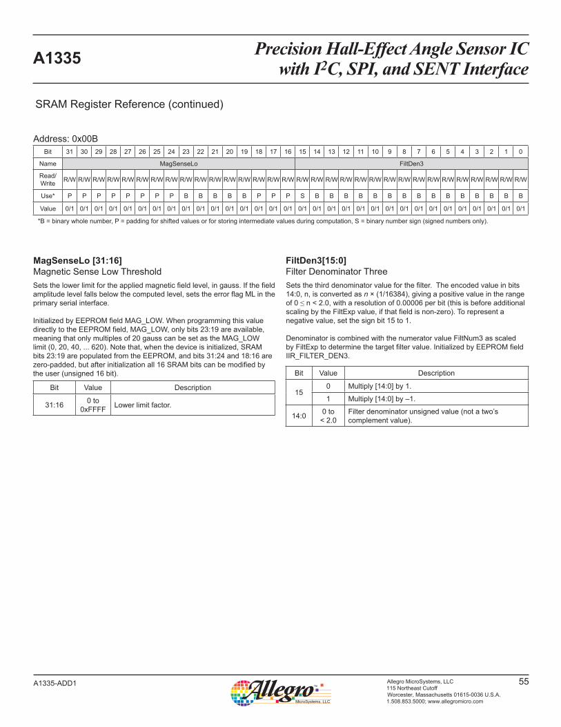
Precision Hall-Effect Angle Sensor ICwith I2C, SPI, and SENT InterfaceA1335
55Allegro MicroSystems, LLC115 Northeast CutoffWorcester, Massachusetts 01615-0036 U.S.A.1.508.853.5000; www.allegromicro.com
A1335-ADD1
MagSenseLo [31:16]Magnetic Sense Low ThresholdSets the lower limit for the applied magnetic field level, in gauss. If the field amplitude level falls below the computed level, sets the error flag ML in the primary serial interface.
Initialized by EEPROM field MAG_LOW. When programming this value directly to the EEPROM field, MAG_LOW, only bits 23:19 are available, meaning that only multiples of 20 gauss can be set as the MAG_LOW limit (0, 20, 40, ... 620). Note that, when the device is initialized, SRAM bits 23:19 are populated from the EEPROM, and bits 31:24 and 18:16 are zero-padded, but after initialization all 16 SRAM bits can be modified by the user (unsigned 16 bit).
Bit Value Description
31:16 0 to 0xFFFF Lower limit factor.
Address: 0x00BBit 31 30 29 28 27 26 25 24 23 22 21 20 19 18 17 16 15 14 13 12 11 10 9 8 7 6 5 4 3 2 1 0
Name MagSenseLo FiltDen3
Read/Write R/W R/W R/W R/W R/W R/W R/W R/W R/W R/W R/W R/W R/W R/W R/W R/W R/W R/W R/W R/W R/W R/W R/W R/W R/W R/W R/W R/W R/W R/W R/W R/W
Use* P P P P P P P P B B B B B P P P S B B B B B B B B B B B B B B B
Value 0/1 0/1 0/1 0/1 0/1 0/1 0/1 0/1 0/1 0/1 0/1 0/1 0/1 0/1 0/1 0/1 0/1 0/1 0/1 0/1 0/1 0/1 0/1 0/1 0/1 0/1 0/1 0/1 0/1 0/1 0/1 0/1
*B = binary whole number, P = padding for shifted values or for storing intermediate values during computation, S = binary number sign (signed numbers only).
FiltDen3[15:0]Filter Denominator ThreeSets the third denominator value for the filter. The encoded value in bits 14:0, n, is converted as n × (1/16384), giving a positive value in the range of 0 ≤ n < 2.0, with a resolution of 0.00006 per bit (this is before additional scaling by the FiltExp value, if that field is non-zero). To represent a negative value, set the sign bit 15 to 1. Denominator is combined with the numerator value FiltNum3 as scaled by FiltExp to determine the target filter value. Initialized by EEPROM field IIR_FILTER_DEN3.
Bit Value Description
150 Multiply [14:0] by 1.
1 Multiply [14:0] by –1.
14:0 0 to < 2.0
Filter denominator unsigned value (not a two’s complement value).
SRAM Register Reference (continued)

Precision Hall-Effect Angle Sensor ICwith I2C, SPI, and SENT InterfaceA1335
56Allegro MicroSystems, LLC115 Northeast CutoffWorcester, Massachusetts 01615-0036 U.S.A.1.508.853.5000; www.allegromicro.com
A1335-ADD1
Address: 0x0C through 0x01A(Segmented Linearization 0x06[SL] = 1, Harmonic Linearization 0x06[HL] = 0 or 1)
Bit 31 30 29 28 27 26 25 24 23 22 21 20 19 18 17 16 15 14 13 12 11 10 9 8 7 6 5 4 3 2 1 0
Name(0x0C to
0x12)SegLinCoeff_[Even: 2 through 14] SegLinCoeff_[Odd: 1 through 13]
Name(0x13) SegLinOffset SegLinCoeff_15
Name(0x14 to0x1A)
HarLinPhase_[9 through 15] Adv HarLinAmp_[9 through 15]
(Segmented Linearization 0x06[SL] = 0, Harmonic Linearization 0x06[HL] = 0 or 1)Bit 31 30 29 28 27 26 25 24 23 22 21 20 19 18 17 16 15 14 13 12 11 10 9 8 7 6 5 4 3 2 1 0
Name(0x0C to
0x1A)HarLinPhase_[1 through 15] Adv HarLinAmp_[1 through 15]
Read/Write R/W R/W R/W R/W R/W R/W R/W R/W R/W R/W R/W R/W R/W R/W R/W R/W R/W R/W R/W R/W R/W R/W R/W R/W R/W R/W R/W R/W R/W R/W R/W R/W
Use* B B B B B B B B B B B B P P P P B B B B B B B B B B B B P P P P
Value 0/1 0/1 0/1 0/1 0/1 0/1 0/1 0/1 0/1 0/1 0/1 0/1 0/1 0/1 0/1 0/1 0/1 0/1 0/1 0/1 0/1 0/1 0/1 0/1 0/1 0/1 0/1 0/1 0/1 0/1 0/1 0/1
*B = binary whole number, P = padding for shifted values and for storing values during operation.
SRAM Register Reference (continued)
SegLinCoeff_n [31:16, 15:0]Segmented Linearization CoefficientsStore individual segmented linearization coefficients. The encoded value in this field, n, is converted as n × ( 360 /65536 ) = angular degrees. These coefficients represent the start points of each segment of a 16-segment curve, where each segment spans 22.5 degrees of the reference axis as determined by the LS bit in the SRAM AlgEnb register. The end point of any segment is the start point of the next higher segment. The start point of the first segment is always 0, and the end point of the curve is always 360 degrees, therefore only 15 coefficients are used to represent the intermediate segment boundaries.
If LS = 0, then the coefficients represent the angle-sensor reading when the encoder (absolute angle) reading is at the segment boundary value (22.5, 45.0 ... 337.5 degrees).
If LS=1, then the coefficients represent the encoder (absolute angle) value when the angle-sensor reads the segment boundary value, which must be determined by experimentally sweeping the encoder and reading the sensor until the output reads the segment boundary value.
Set [0x06]SL to 1 to apply segmented linearization.
Initialized for each segment by EEPROM SEG_LIN_COEFF_n fields. When programming this value directly to the EEPROM field, EEPROM SEG_LIN_COEFF_n, only the 12 MSBs (23:12) are available. Note that, when the device is initialized, SRAM bits 31:20 are populated from EEPROM, and SRAM bits 19:16 are zero-padded, but after initialization all 16 SRAM bits can be modified by the user (unsigned 16 bit).
If SL is set to 0 these registers convert to represent HarLinPhase_n (fields 31:16), and Adv (15:14) with HarLinAmp_n (13:0).
Bit Value Description
31:16 0 to0xFFFF
Segment coefficient (equivalent 0 to 360 degrees), in angle resolution units.
SegLinOffset 0x13[31:16]Segmented Linearization OffsetThe prelinearization angle value that will be the initial (zero) point for segmented linearization; that is, the zero point on the error curve. The encoded value in this field, n, is converted as n × ( 360 /65536 ) = angular degrees.
Initialized by EEPROM field SEG_LIN_OFFSET. When programming this value directly to the EEPROM field, SEG_LIN_OFFSET, only the 12 MSBs (23:12) are available. Note that, when the device is initialized, SRAM bits 31:20 are populated from EEPROM, and SRAM bits 19:16 are zero-padded, but after initialization all 16 SRAM bits can be modified by the user (unsigned 16 bit).
If [0x06]SL is set to 0, this field converts to represent [0x13]HarLinPhase.
Bit Value Description
31:16 0 to0xFFFF Initial angle value for segmented linearization.

Precision Hall-Effect Angle Sensor ICwith I2C, SPI, and SENT InterfaceA1335
57Allegro MicroSystems, LLC115 Northeast CutoffWorcester, Massachusetts 01615-0036 U.S.A.1.508.853.5000; www.allegromicro.com
A1335-ADD1
Address: 0x0C through 0x01A (continued)
SRAM Register Reference (continued)
HarLinPhase_n [31:16]Harmonic Linearization Phase CoefficientsStore individual harmonic linearization phase coefficients. The encoded value in this field, n, is converted as n × ( 360 /65536 ) = angular degrees.
Initialized for each component by EEPROM HARMONIC_PHASE_n fields. When programming this value directly to the EEPROM fields, HARMONIC_PHASE_n, only the 12 MSBs (23:12) are available. Note that, when the device is initialized, SRAM bits 31:20 are populated from EEPROM, and SRAM bits 19:16 are zero-padded, but after initialization all 16 SRAM bits can be modified by the user (unsigned 16 bit). Set [0x06] HL to 1 to apply harmonic linearization.
Note: A maximum of 11 harmonics can be populated from EEPROM (registers 0x0C through 0x16). Up to 15 harmonics may be written to SRAM (registers 0x17 through 0x1A), and used for compensation. This value is only stored in volatile memory and will be lost after power off.
Bit Value Description
31:16 0 to0xFFFF
Harmonic component phase coefficient (equivalent 0 to 360 degrees), in angle resolution units.
HarLinAmp_n [13:0]Harmonic Linearization Amplitude CoefficientsStore individual harmonic linearization amplitude coefficients. The encoded value in this field, n, is converted as n × ( 360 /131072 ) = angular degrees.
Initialized for each component by EEPROM HARMONIC_AMPLITUDE_n fields. When programming this value directly to the EEPROM fields, HARMONIC_AMPLITUDE_n, only the 12 MSBs (23:12) are available. Note that, when the device is initialized, SRAM bits 13:4 are populated from EEPROM, and SRAM bits 3:0 are zero-padded, but after initialization all 14 SRAM bits can be modified by the user (unsigned 14 bit).
If [0x06]SL = 0, the 8 SegLinCoeff_n fields (15:0) in registers 0x0C through 0x13 convert to represent HarLinAmp (and Adv) fields.
Note: A maximum of 11 harmonics can be populated from EEPROM (registers 0x0C through 0x16). Up to 15 harmonics may be written to SRAM (registers 0x17 through 0x1A), and used for compensation. This value is only stored in volatile memory and will be lost after power off.
Bit Value Description
13:0 0 to0x3FFF
Harmonic component amplitude coefficient (equivalent 0 to 45 degrees), in angle resolution units.
Adv [15:14]Harmonic Advance CountSets the increment between sequential pairs of applied harmonic components. The value entered, n (in the range 0 to 3), indicates how many harmonics to be skipped from the previous component to the current component.
The count is applied as 1 + n. For example, the first component (0x0C) minimum (n = 0) is the 1st harmonic and the maximum (n = 3) is the 4th harmonic. The effect is cumulative; when all components are set to n = 3, the 60th harmonic is available at the fifteenth component (0x1A).
Initialized for each component by EEPROM ADV fields.
If [0x06]SL = 0, the 8 SegLinCoeff_n fields (15:0) in registers 0x0C through 0x13 convert to represent Adv (and HarLinAmp) fields.
Note: A maximum of 11 harmonics can be populated from EEPROM (registers 0x0C through 0x16). Up to 15 harmonics may be written to SRAM (registers 0x17 through 0x1A), and used for compensation. This value is only stored in volatile memory and will be lost after power off.
Bit Value Description
15:14 0 to0x11
Count for skipped harmonics between components.

Precision Hall-Effect Angle Sensor ICwith I2C, SPI, and SENT InterfaceA1335
58Allegro MicroSystems, LLC115 Northeast CutoffWorcester, Massachusetts 01615-0036 U.S.A.1.508.853.5000; www.allegromicro.com
A1335-ADD1
The EEPROM is the internal non-volatile storage, used for configuring the power-up state of the A1335. Some locations are pre-programmed and not rewriteable. Those locations described in this section are rewriteable. At power-up, or following a hard reset, the contents of this EEPROM are read and used to con-figure the A1335. Most of the parameters are moved into the SRAM for quick access by the processor and can be temporarily changed via the serial interface, although some words are used to configure hardware registers, or are moved to non-accessible SRAM locations.
Each EEPROM word contains 24 data bits. One word may contain multiple configuration fields. All fields in a word must be read and written together. The EEPROM is read and written via the extended access protocol described in section I2C Extended Access Protocol using extended addresses 0x306 through 0x31A. Writing the EEPROM also requires application of higher voltage pulses on the VCC pin as described in the A1335 datasheet.
The location and format of configuration parameters in the SRAM differ from those in the EEPROM, so conversion is neces-sary. Of specific note is that the resolution of values related to angle processing is different in the SRAM versus the EEPROM, with the SRAM maintaining higher resolutions to reduce the error associated with mathematical processing of the angle. The A1335 does all needed conversions when loading the EEPROM into SRAM. However, when updating the EEPROM any format conversions must be done external to the A1335. The following section details the address and format of the EEPROM writeable words. If the field is moved to SRAM, the detailed purpose of the field will be referenced back to that section.
Programming EEPROMThe device utilizes EEPROM to permanently store configura-tion parameters for operation. As a result, writing to EEPROM requires a specific order of events so there are no accidental writes to the interface.
The first step is to unlock the device. After the A1335 has been unlocked for writing, the processor must be set to Idle mode (set primary serial interface register CTRL [CDS field] ). EEPROM cannot be written unless the A1335 is in Idle mode.
After Programming mode is unlocked at power-on, EEPROM registers can be preloaded with data. The serial interface is used for preloading (via the SPI, I2C or Manchester interface).
The final step in writing to EEPROM is sending programming pulses on the EEPROM programming pin (the VCC pin) to set the bitfields. The VCC pulse profile necessary for EEPROM pro-gramming is shown in Figure 17. Minimum and maximum times are described in Table 17. After EEPROM has been written, it is recommended to cycle power to the device.
300 µs8 ms
60 µs2 µs
300 µs8 ms
60 µs
ERASE PROGRAM
18 V
6 V
Figure 17: VCC Pulse Profile for EEPROM Programming
Table 17: EEPROM PulseParameter Comments Min. Typ. Max. Unit
Pulse High Time Time above minimum pulse voltage
8 10 11 ms
Rise Time 10% to 90% of minimum pulse level
300 – – µs
Fall Time 10% to 90% of minimum pulse level
60 – – µs
Pulse Voltage 18 19 19.5 VSeparation time Time between first pulse
dropping below 6 V and 2nd pulse rising above 6 V
2 µs – 50 ms µs/ms
Unlocking EEPROMThe EEPROM in the device is unlocked using the serial inter-face. The device is unlocked by writing the Customer Keycode 0x27811F77 to the extended address 0xFFFE. After the device target device has been unlocked, the user can proceed to program parameters in the EEPROM addressing range (0x306 – 0x319).
The unlocking process is accomplished by the following com-mands in the serial interface:
1. Load the EWA (0x02, 0x03) register with the target extended address (0xFFFE). a. Write 0xFF to 0x02 (MSB of extended address to ERA
0x02).
EEPROM Description and Programming

Precision Hall-Effect Angle Sensor ICwith I2C, SPI, and SENT InterfaceA1335
59Allegro MicroSystems, LLC115 Northeast CutoffWorcester, Massachusetts 01615-0036 U.S.A.1.508.853.5000; www.allegromicro.com
A1335-ADD1
b. Write 0xFE to 0x03 (LSB of extended address to ERA 0x03).
2. Load the EWD (07:04) register with the customer access code.a. Write 0x27 to 0x04 (MSB of extended data to EWD).b. Write 0x81 to 0x05.c. Write 0x1F to 0x06.
d. Write 0x77 to 0x07 (LSB of extended address to EWD).3. Invoke the extended addressing by writing the direct CTRL
register EXW bit with 1. Write 0x80 to EWCS 0x08.
Dual Purpose RegistersThere are eight registers in the EEPROM (addresses 0x30C through 0x313) that can be used for alternative purposes: either segmented linearization or harmonic linearization. The format used corresponds to the linearization method chosen. To choose segmented linearization, set the SL bit to 1 (bit 20 in the SRAM register 0x06, AlgEnb field).
An additional three words in the EEPROM (addresses 0x314 through 0x316) have different uses depending on the value in the HAR_MAX field in the EEPROM. HAR_MAX config-ures the number of harmonics used for harmonic linearization. If HAR_MAX is between 9 and 11, then the purpose of loca-tions 0x314 through 0x316 are incrementally reassigned to be harmonic fields instead of their primary usage, a shown in the following table.
HAR_MAX Value in EEPROM
EEPROM Words Reassigned as Harmonic Format
9 0x314
10 Above, and 0x315
11 Above, and 0x316
The configuration for the primary usage is assigned a default value in the SRAM. These defaults can then be changed, if necessary, via the serial interface after power-up (SRAM must be unlocked to do so).
Reassigned Word Default Value if Reassigned
0x14 GAIN_OFFSET = 0x000GAIN = 0x0 (gives unit gain of 1.0)
0x15MAX_ANGLE = 0MIN_ANGLE = 0(full angle range)
0x16CLAMP_HIGH = 0xFFFCLAMP_LOW = 0(full clamp range)
Self-Test OptionsThe DH and DC (0x309 bits 22 and 21) and DB (0x308 bit 21) bits are used only during the power-up process to disable self-tests. After the power-up process is complete, these bits are not retained in SRAM.
Configuration FlagsThe GR, LI, FR, LE, and LM bits configure options that are not changeable after power-up. They are moved from EEPROM to locations that are not accessible via the serial interface, though they can be read via the extended access protocol.
Angle Resolution for EEPROMThe 12-bit value in this field (in angle resolution units) multiplied by (360/4096) equals the angle in degrees. This is the represen-tation of an angle between 0 and 360 degrees (0 ≤ angle < 360) in the EEPROM field, and in the primary serial interface angle register (ANG) where 12 bits are used to represent the angle. This gives a resolution of 360/4096, approximately 0.088 degrees.
• To convert the field value to degrees: A 12-bit field value of 0110 1110 0001 (0x6E1) equals integer 1761 decimal. So 1761 × (360 / 4096) = 154.78 angular degrees (rounded to nearest 1/100).
• To convert degrees to the equivalent field value: An angle value of 317.88 degrees = 317.88 / (360 / 4096) = 317.88 × (4096 / 360) = 3616.768, or 3617 (rounded to nearest integer). This con-verts to a binary field value of 1110 0010 0001 (0xE21).
Note that the difference in angle resolution between EEPROM and SRAM is 4 bits, and a simple conversion between the two formats is given in the section Angle Resolution for SRAM.

Precision Hall-Effect Angle Sensor ICwith I2C, SPI, and SENT InterfaceA1335
60Allegro MicroSystems, LLC115 Northeast CutoffWorcester, Massachusetts 01615-0036 U.S.A.1.508.853.5000; www.allegromicro.com
A1335-ADD1
Table 18: EEPROM Registers Map (Factory Reserved Registers Not Shown)
EADR StateBits
23 22 21 20 19 18 17 16 15 14 13 12 11 10 9 8 7 6 5 4 3 2 1 00x306 – RD LS SB SS 0 IV RO SL HL LR – FI ZERO OFFSET0x307 – CUST IRR_ERRVAL IIR_FILTER_NUM10x308 – ORATE DB FP_ADJ MAXID IIR_FILTER_NUM20x309 – UI DH DC SC HAR_MAX (HM) IIR_FILTER_NUM30x30A – FR LE LM MAG_HIGH IIR_FILTER_DEN20x30B – DM GR LI MAG_LOW IIR_FILTER_DEN3
0x30CLinear SEG_LIN_COEFF_2 SEG_LIN_COEFF_1
Harmonic HARMONIC_PHASE_1 ADV HARMONIC_AMPLITUDE_1
0x30DLinear SEG_LIN_COEFF_4 SEG_LIN_COEFF_3
Harmonic HARMONIC_PHASE_2 ADV HARMONIC_AMPLITUDE_2
0x30ELinear SEG_LIN_COEFF_6 SEG_LIN_COEFF_5
Harmonic HARMONIC_PHASE_3 ADV HARMONIC_AMPLITUDE_3
0x30FLinear SEG_LIN_COEFF_8 SEG_LIN_COEFF_7
Harmonic HARMONIC_PHASE_4 ADV HARMONIC_AMPLITUDE_4
0x310Linear SEG_LIN_COEFF_10 SEG_LIN_COEFF_9
Harmonic HARMONIC_PHASE_5 ADV HARMONIC_AMPLITUDE_5
0x311Linear SEG_LIN_COEFF_12 SEG_LIN_COEFF_11
Harmonic HARMONIC_PHASE_6 ADV HARMONIC_AMPLITUDE_6
0x312Linear SEG_LIN_COEFF_14 SEG_LIN_COEFF_13
Harmonic HARMONIC_PHASE_7 ADV HARMONIC_AMPLITUDE_7
0x313Linear SEG_LIN_OFFSET SEG_LIN_COEFF_15
Harmonic HARMONIC_PHASE_8 ADV HARMONIC_AMPLITUDE_8
0x314HAR_MAX>8 HARMONIC_PHASE_9 ADV HARMONIC_AMPLITUDE_9HAR_MAX<9 GAIN_OFFSET GAIN (4.8)
0x315HAR_MAX>9 HARMONIC_PHASE_10 ADV HARMONIC_AMPLITUDE_10
HAR_MAX<10 MAX_ANGLE MIN_ANGLE
0x316HAR_MAX>10 HARMONIC_PHASE_11 ADV HARMONIC_AMPLITUDE_11HAR_MAX<11 CLAMP_HIGH CLAMP_HIGH
0x317 – CUSTOMER – SENT_TICK SM SENT_MODE0x318 – SS ES AW TR SU EU WP WT RC XE ME ST – XO IE CR NR AT AH AL OV UV MH ML
0x319 – IS SDRV PO DATA_MODE CIS SCN_MODE NS ZS DA FA XS I2C_SLAVE_ADDR DAW DR
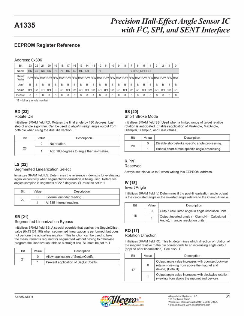
Precision Hall-Effect Angle Sensor ICwith I2C, SPI, and SENT InterfaceA1335
61Allegro MicroSystems, LLC115 Northeast CutoffWorcester, Massachusetts 01615-0036 U.S.A.1.508.853.5000; www.allegromicro.com
A1335-ADD1
EEPROM Register Reference
Address: 0x306Bit 23 22 21 20 19 18 17 16 15 14 13 12 11 10 9 8 7 6 5 4 3 2 1 0
Name RD LS SB SS R IV RO SL HL LR – FI ZERO_OFFSET
Read/Write R/W R/W R/W R/W R/W R/W R/W R/W R/W R/W R/W R/W R/W R/W R/W R/W R/W R/W R/W R/W R/W R/W R/W R/W
Use* B B B B B B B B B B B B B B B B B B B B B B B B
Value 0/1 0/1 0/1 0/1 0 0/1 0/1 0/1 0/1 0/1 0/1 0/1 0/1 0/1 0/1 0/1 0/1 0/1 0/1 0/1 0/1 0/1 0/1 0/1
Default 0 0 0 0 0 0 0 0 0 0 1 0 0 0 0 0 0 0 0 0 0 0 0 0
*B = binary whole number
R [19]ReservedAlways set this value to 0 when writing this EEPROM address.
RD [23]Rotate DieInitializes SRAM field RD. Rotates the final angle by 180 degrees. Last step of angle algorithm. Can be used to align/misalign angle output from both die when using the dual die version.
Bit Value Description
230 No rotation.
1 Add 180 degrees to angle then normalize.
LS [22]Segmented Linearization SelectInitializes SRAM field LS. Determines the reference index-axis for evaluating signal eccentricity when segmented linearization is being used. Reference angles sampled in segments of 22.5 degrees. SL must be set to 1.
Bit Value Description
220 External encoder reading.
1 A1335 internal reading.
SB [21]Segmented Linearization BypassInitializes SRAM field SB. A special override that applies the SegLinOffset value (0x13 [31:16]) when segmented linearization is performed, but does not perform the actual linearization. This function can be used to take the measurements required for segmented without having to otherwise program the linearization table to a straight line. SL must be set to 1.
Bit Value Description
210 Allow application of SegLinCoeffs.
1 Prevent application of SegLinCoeffs.
SS [20]Short Stroke ModeInitializes SRAM field SS. Used when a limited range of target relative rotation is anticipated. Enables application of MinAngle, MaxAngle, ClampHi, ClampLo, and Gain values.
Bit Value Description
200 Disable short-stroke specific angle processing.
1 Enable short-stroke specific angle processing.
IV [18]Invert AngleInitializes SRAM field IV. Determines if the post-linearization angle output is the calculated angle or the inverted angle relative to the ClampHi value.
Bit Value Description
180 Output calculated angle in angle resolution units.
1 Output inverted angle (= ClampHi – Calculated Angle), in angle resolution units.
RO [17]Rotation DirectionInitializes SRAM field RO. This bit determines which direction of rotation of the magnet relative to the die corresponds to an increasing angle output (applied after linearization). See also LR.
Bit Value Description
170
Output angle value increases with counterclockwise rotation (viewing from above the magnet and device) (Default).
1 Output angle value increases with clockwise rotation (viewing from above the magnet and device).
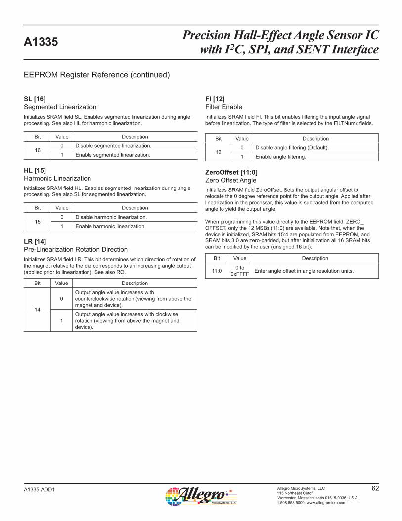
Precision Hall-Effect Angle Sensor ICwith I2C, SPI, and SENT InterfaceA1335
62Allegro MicroSystems, LLC115 Northeast CutoffWorcester, Massachusetts 01615-0036 U.S.A.1.508.853.5000; www.allegromicro.com
A1335-ADD1
EEPROM Register Reference (continued)
SL [16]Segmented LinearizationInitializes SRAM field SL. Enables segmented linearization during angle processing. See also HL for harmonic linearization.
Bit Value Description
160 Disable segmented linearization.
1 Enable segmented linearization.
HL [15]Harmonic LinearizationInitializes SRAM field HL. Enables segmented linearization during angle processing. See also SL for segmented linearization.
Bit Value Description
150 Disable harmonic linearization.
1 Enable harmonic linearization.
LR [14]Pre-Linearization Rotation DirectionInitializes SRAM field LR. This bit determines which direction of rotation of the magnet relative to the die corresponds to an increasing angle output (applied prior to linearization). See also RO.
Bit Value Description
14
0Output angle value increases with counterclockwise rotation (viewing from above the magnet and device).
1Output angle value increases with clockwise rotation (viewing from above the magnet and device).
FI [12]Filter EnableInitializes SRAM field FI. This bit enables filtering the input angle signal before linearization. The type of filter is selected by the FILTNumx fields.
Bit Value Description
120 Disable angle filtering (Default).
1 Enable angle filtering.
ZeroOffset [11:0] Zero Offset AngleInitializes SRAM field ZeroOffset. Sets the output angular offset to relocate the 0 degree reference point for the output angle. Applied after linearization in the processor, this value is subtracted from the computed angle to yield the output angle.
When programming this value directly to the EEPROM field, ZERO_OFFSET, only the 12 MSBs (11:0) are available. Note that, when the device is initialized, SRAM bits 15:4 are populated from EEPROM, and SRAM bits 3:0 are zero-padded, but after initialization all 16 SRAM bits can be modified by the user (unsigned 16 bit).
Bit Value Description
11:0 0 to0xFFFF Enter angle offset in angle resolution units.

Precision Hall-Effect Angle Sensor ICwith I2C, SPI, and SENT InterfaceA1335
63Allegro MicroSystems, LLC115 Northeast CutoffWorcester, Massachusetts 01615-0036 U.S.A.1.508.853.5000; www.allegromicro.com
A1335-ADD1
Address: 0x307Bit 23 22 21 20 19 18 17 16 15 14 13 12 11 10 9 8 7 6 5 4 3 2 1 0
Name CUST IIR_ERRVAL IIR_FILTER_NUM1
Read/Write R/W R/W R/W R/W R/W R/W R/W R/W R/W R/W R/W R/W R/W R/W R/W R/W R/W R/W R/W R/W R/W R/W R/W R/W
Use* B B B B B B B B S B F F F F F F F F F F F F F F
Value 0/1 0/1 0/1 0/1 0/1 0/1 0/1 0/1 0/1 0/1 0/1 0/1 0/1 0/1 0/1 0/1 0/1 0/1 0/1 0/1 0/1 0/1 0/1 0/1
Default 0 0 0 0 0 0 0 0 0 0 0 0 0 0 0 0 1 0 1 0 1 0 1 0
*B = binary whole number, F = fractional binary number, S = binary number sign (signed numbers only)
IIR_ERRVAL[19:16]Filter ResetInitializes SRAM field FfiltError.
CUST[23:20]Customer Field OneFree form customer scratchpad.
IIR_FILTER_NUM1[15:0]Filter Numerator OneInitializes SRAM field FiltNum1.
Address: 0x308Bit 23 22 21 20 19 18 17 16 15 14 13 12 11 10 9 8 7 6 5 4 3 2 1 0
Name ORATE DB FP_ADJ MAXID IIR_FILTER_NUM2
Read/Write R/W R/W R/W R/W R/W R/W R/W R/W R/W R/W R/W R/W R/W R/W R/W R/W R/W R/W R/W R/W R/W R/W R/W R/W
Use* B B B B B B B B S B F F F F F F F F F F F F F F
Value 0/1 0/1 0/1 0/1 0/1 0/1 0/1 0/1 0/1 0/1 0/1 0/1 0/1 0/1 0/1 0/1 0/1 0/1 0/1 0/1 0/1 0/1 0/1 0/1
Default 0 0 0 0 0 0 0 0 0 0 0 0 0 0 0 1 0 1 0 1 0 1 1 0
*B = binary whole number, F = fractional binary number, S = binary number sign (signed numbers only), X = not used
EEPROM Register Reference (continued)
ORATE [23:21]Output RateConfigures the refresh rate of the device output as Log 2(n) where 2n is the quantity of samples to be averaged and n is the value entered. Increasing the quantity of samples to be averaged effectively increases the resolution (reduces the noise) of the device. After initialization, can be read and changed via the Extended Access command 0xFFD0.
Note: The nominal update rate can vary about ±2% from the specified values depending on the frequency of the internal oscillator, with additional drift due to temperature changes. The average update rate can vary ±4 µs on any given sample, depending on direction and speed of rotation of the magnetic field.
Bit Value Description
23:21
000 1 sample, 31.25 µs update
001 2 samples, 62.5 µs update
010 4 samples, 125 µs update
011 8 samples, 250 µs update
100 16 samples, 500 µs update
101 32 samples, 1 ms update
110 64 samples, 2 ms update
111 128 samples, 4 ms update
DB [20]Disable SRAM BISTDisables built-in self test (BIST) diagnostic algorithm to test SRAM during power-on. When enabled, occurs at every device boot-up initialization. Not accessible in SRAM. If enabled, this self-test takes approximately 100 µs to complete at initialization, delaying initial angle data.
Bit Value Description
200 Enable SRAM BIST (Default)
1 Disable SRAM BIST
Continued on the next page...

Precision Hall-Effect Angle Sensor ICwith I2C, SPI, and SENT InterfaceA1335
64Allegro MicroSystems, LLC115 Northeast CutoffWorcester, Massachusetts 01615-0036 U.S.A.1.508.853.5000; www.allegromicro.com
A1335-ADD1
FP_ADJ [19:18]Function Pulse AdjustOnly for Long SSENT (SENT_MODE = 7). Increases the lower threshold of what the sensor views as a valid F_OUTPUT pulse by 0-3 Ticks. Reduces the possible misinterpretation of F_OUTPUT pulses at sub-1.5 µs Tick times. All sensors sharing a common bus should be configured with the same adjustment.
Bit Value Description
19:18
00 No Change to F_OUTPUT pulse width. Minimum width = 9 Ticks.
01 Minimum width of F_OUTPUT increased by 1 Tick. Min = 10 Ticks.
10 Minimum width of F_OUTPUT increased by 2 Ticks. Min = 11 Ticks.
11 Minimum width of F_OUTPUT increased by 3 Ticks. Min = 12 Ticks.
MAXID [17:16]Maximum Sensor IDSpecifies the highest sensor ID number on the shared SENT bus. When using SSENT, this determines when the slot counter of each sensor resets to zero. All sensors sharing a common SENT bus should be configured with the same MAXID number. ID values are assigned by the logic state of the SA0 and SA1 pins.
Bit Value Description
17:16
00 Highest ID value is 0. Sensor is not sharing the SENT line
01 Highest ID value is 1. Two sensors are sharing the SENT line
10 Highest ID value is 2. Three sensors are sharing the SENT line
11 Highest ID value is 3. Four sensors are sharing the SENT line
EEPROM Register Reference (continued)
Address: 0x308 (continued)
IIR_FILTER_NUM2[15:0]Filter Numerator TwoInitializes SRAM field FiltNum2.

Precision Hall-Effect Angle Sensor ICwith I2C, SPI, and SENT InterfaceA1335
65Allegro MicroSystems, LLC115 Northeast CutoffWorcester, Massachusetts 01615-0036 U.S.A.1.508.853.5000; www.allegromicro.com
A1335-ADD1
HAR_MAX[19:16]Harmonic Linearization Maximum OffsetInitializes SRAM field HLinMax.
Note: In the EEPROM only, this field also controls the reassignment of EEPROM words 0x14 through 0x16 as harmonic coefficients.
IIR_FILTER_NUM3[15:0]Filter Numerator ThreeInitializes SRAM field FiltNum3.
Address: 0x309Bit 23 22 21 20 19 18 17 16 15 14 13 12 11 10 9 8 7 6 5 4 3 2 1 0
Name UI DH DC SC HAR_MAX IIR_FILTER_NUM3
Read/Write R/W R/W R/W R/W R/W R/W R/W R/W R/W R/W R/W R/W R/W R/W R/W R/W R/W R/W R/W R/W R/W R/W R/W R/W
Use* B B B B B B B B S B F F F F F F F F F F F F F F
Value 0/1 0/1 0 0/1 0/1 0/1 0/1 0/1 0/1 0/1 0/1 0/1 0/1 0/1 0/1 0/1 0/1 0/1 0/1 0/1 0/1 0/1 0/1 0/1
Default 0 0 0 0 0 0 0 0 0 0 0 0 0 0 0 0 1 0 1 0 1 0 1 1
*B = binary whole number, F = fractional binary number, S = binary number sign
EEPROM Register Reference (continued)
UI [23]User Initiated Diagnostic EnableEnables the SENT interface to respond to F_DIAG/DiagStomp pulses to initiate the CVH Self-test.
Bit Value Description
23
0 CVH Self-test cannot be initiated via SENT
1CVH Self-test may be initiated via SENT interface through the receipt of a F_Diag or a DiagStomp pulse, depending on SENT configuration.
DH [22]Disable CVH Self-Test at Power OnDisables built-in diagnostics to test the Hall-effect (CVH) elements. When enabled, test occurs at every device boot-up initialization. Not accessible in SRAM. If enabled, this self-test takes approximately 36 ms to complete at initialization, delaying initial angle data.
Bit Value Description
220 Enable Hall elements self-test (Default).
1 Disable Hall elements self-test.
DC [21]Disable ROM ChecksumDisables built-in diagnostics to test the ROM. When enabled, occurs at every device boot-up initialization. Not accessible in SRAM. If enabled, this self-test takes approximately 4.5 ms to complete at initialization, delaying initial angle data.
Bit Value Description
210 Enable ROM checksum testing (Default).
1 Disable ROM checksum testing.
SC [20]Data Redundancy Check Enable (SPI)Enables cyclic redundancy check (CRC) on data input through the SPI.
If HAR_MAX > 13, converted to use for initializing SRAM register 0x19 field HarLinPhase.
Bit Value Description
200 Ignore CRC on input. (Default)
1 Validate CRC on input

Precision Hall-Effect Angle Sensor ICwith I2C, SPI, and SENT InterfaceA1335
66Allegro MicroSystems, LLC115 Northeast CutoffWorcester, Massachusetts 01615-0036 U.S.A.1.508.853.5000; www.allegromicro.com
A1335-ADD1
MAG_HIGH[20:16]Magnetic Sense Limit HighInitializes SRAM field MagSenseHi. Sets the upper limit for the applied magnetic field level, in multiples of 40 gauss (0-1240 G). If the field amplitude level rises above the computed level, sets the error flag MH in the primary serial interface.
IIR_FILTER_DEN2[15:0]Filter Denominator TwoInitializes SRAM field FiltDen2.
Address: 0x30ABit 23 22 21 20 19 18 17 16 15 14 13 12 11 10 9 8 7 6 5 4 3 2 1 0
Name FR LE LM MAG_HIGH IIR_FILTER_DEN2
Read/Write R/W R/W R/W R/W R/W R/W R/W R/W R/W R/W R/W R/W R/W R/W R/W R/W R/W R/W R/W R/W R/W R/W R/W R/W
Use* B B B B B B B B S B F F F F F F F F F F F F F F
Value 0/1 0/1 0 0/1 0/1 0/1 0/1 0/1 0/1 0/1 0/1 0/1 0/1 0/1 0/1 0/1 0/1 0/1 0/1 0/1 0/1 0/1 0/1 0/1
Default 0 0 0 1 1 1 1 1 1 1 1 0 1 1 0 0 0 0 1 1 1 0 0 1
*B = binary whole number, F = fractional binary number, S = binary number sign (signed numbers only), X = not used
FR [23]Fault Recovery ModeThis bit determines device behavior when processor watchdog errors, due to a timeout or halt condition, are detected. If the hardware watchdog logic has detected that the processor is not operating correctly, the WP and WT bits in the XERR register in the primary serial interface are set to 1.
If this bit is set to 0, then the logic is configured to report the error, but not to take corrective active, meaning that angle data may no longer be correct, and the processor could be halted or be no longer processing commands. In this case, it is up to the host to take corrective response, such as resetting the part via the CTRL register.
If this bit is set to 1, then a watchdog error is reported in the XERR register, but in addition the A1335 attempts to perform the equivalent of a soft reset in order to resume angle processing. The EEPROM is not re-read, so if configuration data in the SRAM was changed as a result of whatever fault occurred, there is still the potential for the angle data to be wrong.
This setting may be read through the 0xFFF8 extended access command after initialization.
Bit Value Description
230 Take no remedial action when if a watchdog fault
occurs. (Default)
1 Reset the processor if a watchdog fault occurs.
LE [22]Lock EEPROMThis bit determines if any EEPROM fields can be modified.
NOTE: When this bit is set in EEPROM, the EEPROM is locked and no further EEPROM writes are possible.
This setting may be read through the 0xFFF8 extended access command after initialization.
Bit Value Description
220 Writing or erasing EEPROM fields allowed (Default).
1 EEPROM fields locked.
LM [21]Lock ProcessorThis bit determines if SRAM is accessible, and if certain extended operations are available. This setting can be reset.
This setting is available through the 0xFFF8 extended access command after initialization.
Bit Value Description
210 SRAM and extended commands available (Default).
1 SRAM and extended commands locked.
EEPROM Register Reference (continued)

Precision Hall-Effect Angle Sensor ICwith I2C, SPI, and SENT InterfaceA1335
67Allegro MicroSystems, LLC115 Northeast CutoffWorcester, Massachusetts 01615-0036 U.S.A.1.508.853.5000; www.allegromicro.com
A1335-ADD1
IIR_FILTER_DEN3 [15:0]Filter Denominator ThreeInitializes SRAM field FiltDen3.
Address: 0x30BBit 23 22 21 20 19 18 17 16 15 14 13 12 11 10 9 8 7 6 5 4 3 2 1 0
Name DM GR LI MAG_LOW IIR_FILTER_DEN3
Read/Write R/W R/W R/W R/W R/W R/W R/W R/W R/W R/W R/W R/W R/W R/W R/W R/W R/W R/W R/W R/W R/W R/W R/W R/W
Use* B B B B B B B B S B F F F F F F F F F F F F F F
Value 0 0/1 0 0/1 0/1 0/1 0/1 0/1 0/1 0/1 0/1 0/1 0/1 0/1 0/1 0/1 0/1 0/1 0/1 0/1 0/1 0/1 0/1 0/1
Default 0 1 0 0 0 0 0 0 0 0 1 0 1 1 1 0 1 1 1 0 0 1 0 0
*B = binary whole number, F = fractional binary number, S = binary number sign (signed numbers only), X = not used
MAG_LOW [20:16]Magnetic Sense Limit LowInitializes SRAM field MagSenseLo. Sets the lower limit for the applied magnetic field level, in multiples of 20 gauss (0-620 G). If the field amplitude level falls below the computed level, sets the error flag ML in the primary serial interface.
GR [22] Go RunThis bit determines device behavior at initialization. Not accessible from SRAM.
Bit Value Description
22
0Boot into Idle mode. (After initialization, to process angles, select Run mode by setting CDS field in Primary Serial Interface to 1.
1Boot into Run mode. Recommended for normal operation after all programming has been completed. (Default)
LI [21] Lock Idle This bit determines if Idle mode can be entered without unlocking the A1335. When set to 1, then after the A1335 enters Run mode, it can not be commanded to exit to Idle mode (which stops angle processing) without the Customer Keycode first being entered (via extended access command 0xFFFE). Not accessible from SRAM.
To program, EEPROM field 0x30A[LE] must be set to 0.
This setting is available through the 0xFFF8 extended access command after initialization.
Bit Value Description
210 Entering Customer ID not required. (Default)
1 Entering Customer ID required.
EEPROM Register Reference (continued)
DM [23] Disable ManchesterIf “1” any Manchester input on the VCC line will be ignored. This takes effect after boot-up and self-test time. If a valid Manchester “Enter” command is recieved before this, the Manchester interface will be enabled.
Bit Value Description
230
Manchester interface is enabled. The part will monitor the Vcc line, looking for a valid Manchester “Enter” command.
1 Manchester interface disabled. Part will ignore all Manchester commands on the Vcc line.

Precision Hall-Effect Angle Sensor ICwith I2C, SPI, and SENT InterfaceA1335
68Allegro MicroSystems, LLC115 Northeast CutoffWorcester, Massachusetts 01615-0036 U.S.A.1.508.853.5000; www.allegromicro.com
A1335-ADD1
Address: 0x30C through 0x313(Segmented Linearization 0x06[SL] = 1, Harmonic Linearization 0x06[HL] = 1)
Bit 23 22 21 20 19 18 17 16 15 14 13 12 11 10 9 8 7 6 5 4 3 2 1 0
Name(0x30C to
0x12)SEG_LIN_COEFF_N [Even: 2 through 14] SEG_LIN_COEFF_N [Odd: 1 through 13]
Name(0x13) SEG_LIN_OFFSET SEG_LIN_COEFF_15
Read/Write R/W R/W R/W R/W R/W R/W R/W R/W R/W R/W R/W R/W R/W R/W R/W R/W R/W R/W R/W R/W R/W R/W R/W R/W
Use* B B B B B B B B B B B B B B B B B B B B B B B B
Value 0/1 0/1 0/1 0/1 0/1 0/1 0/1 0/1 0/1 0/1 0/1 0/1 0/1 0/1 0/1 0/1 0/1 0/1 0/1 0/1 0/1 0/1 0/1 0/1
Default 0 0 0 0 0 0 0 0 0 0 0 0 0 0 0 0 0 0 0 0 0 0 0 0
*B = binary whole number
(Segmented Linearization 0x06[SL] = 0, Harmonic Linearization 0x06[HL] = 1)Bit 23 22 21 20 19 18 17 16 15 14 13 12 11 10 9 8 7 6 5 4 3 2 1 0
Name(0x30C to
0x013)HARMONIC_PHASE_[1 through 8] ADV HARMONIC_AMPLITUDE_[1 through 8]
Read/Write R/W R/W R/W R/W R/W R/W R/W R/W R/W R/W R/W R/W R/W R/W R/W R/W R/W R/W R/W R/W R/W R/W R/W R/W
Use* B B B B B B B B B B B B B B B B B B B B B B B B
Value 0/1 0/1 0/1 0/1 0/1 0/1 0/1 0/1 0/1 0/1 0/1 0/1 0/1 0/1 0/1 0/1 0/1 0/1 0/1 0/1 0/1 0/1 0/1 0/1
*B = binary whole number
EEPROM Register Reference (continued)
SEG_LIN_COEFF [23:12, 11:0]Segmented Linearization CoefficientsInitialize SRAM fields SegLinCoeff if segmented linearization enabled (SL = 1).
HARMONIC_PHASE [23:12]Harmonic Linearization Phase CoefficientsInitialize SRAM fields HarLinPhase. For registers 0x30C through 0x013, optional use for harmonic linearization if segmented linearization disabled (SL = 0). For registers 0x314 through 0x316, optional use for harmonic linearization determined by HAR_MAX setting (eliminates default features).
HARMONIC_AMPLITUDE [9:0]Harmonic Linearization Amplitude CoefficientsInitialize SRAM fields HarLinAmplitude. For registers 0x30C through 0x013, optional use for harmonic linearization if segmented linearization disabled (SL = 0). For registers 0x314 through 0x316, optional use for harmonic linearization determined by HAR_MAX setting (eliminates default features).
ADV [11:10]Harmonic Advance CountInitialize SRAM fields Adv. For registers 0x30C through 0x013, optional use for harmonic linearization if segmented linearization disabled (SL = 0). For registers 0x314 through 0x316, optional use for harmonic linearization determined by HAR_MAX setting (eliminates default features).
SEG_LIN_OFFSET 0x13[23:12]Segmented Linearization OffsetInitialize SRAM field SegLinOffset if segmented linearization enabled (SL = 1).

Precision Hall-Effect Angle Sensor ICwith I2C, SPI, and SENT InterfaceA1335
69Allegro MicroSystems, LLC115 Northeast CutoffWorcester, Massachusetts 01615-0036 U.S.A.1.508.853.5000; www.allegromicro.com
A1335-ADD1
EEPROM Register Reference (continued)Address: 0x314(Segmented Linearization 0x06[SL] = 1, Harmonic Linearization 0x06[HL] = 1) HAR_MAX < 9
Bit 23 22 21 20 19 18 17 16 15 14 13 12 11 10 9 8 7 6 5 4 3 2 1 0
Name GAIN_OFFSET GAIN
Read/Write R/W R/W R/W R/W R/W R/W R/W R/W R/W R/W R/W R/W R/W R/W R/W R/W R/W R/W R/W R/W R/W R/W R/W R/W
Use* B B B B B B B B B B B B B B B B B B B B B B B B
Value 0/1 0/1 0/1 0/1 0/1 0/1 0/1 0/1 0/1 0/1 0/1 0/1 0/1 0/1 0/1 0/1 0/1 0/1 0/1 0/1 0/1 0/1 0/1 0/1
Default 0 0 0 0 0 0 0 0 0 0 0 0 0 0 0 0 0 0 0 0 0 0 0 0
*B = binary whole number
(Segmented Linearization 0x06[SL] = 0, Harmonic Linearization 0x06[HL] = 1) HAR_MAX > 8Bit 23 22 21 20 19 18 17 16 15 14 13 12 11 10 9 8 7 6 5 4 3 2 1 0
Name HARMONIC_PHASE_9 ADV HARMONIC_AMPLITUDE_9
Read/Write R/W R/W R/W R/W R/W R/W R/W R/W R/W R/W R/W R/W R/W R/W R/W R/W R/W R/W R/W R/W R/W R/W R/W R/W
Use* B B B B B B B B B B B B B B B B B B B B B B B B
Value 0/1 0/1 0/1 0/1 0/1 0/1 0/1 0/1 0/1 0/1 0/1 0/1 0/1 0/1 0/1 0/1 0/1 0/1 0/1 0/1 0/1 0/1 0/1 0/1
*B = binary whole number
HARMONIC_PHASE_9 [23:12]Harmonic Linearization Phase Coefficient 12See description at 0x30C.
HARMONIC_AMPLITUDE_9 [9:0]Harmonic Linearization Amplitude Coefficient 12See description at 0x30C.
ADV [11:10]Harmonic Advance CountSee description at 0x30C.
GAIN_OFFSET [23:12]Gain OffsetInitializes SRAM field GainOffset.
If HAR_MAX > 8, converted to use for initializing SRAM field [0x17]HarLinPhase. Sets the offset value used to set the zero-reference point of the angle output value range (that is, to set the zero error point to which the Gain is applied), after Pre-Linearization Rotation (0x306[LR]), but before the Gain value is applied. Gain Offset is subtracted from the angle before multiplication by the Gain. Note that this operation is performed whether 0x306[SS] is set or not.
12-bit field representing 0-360 degrees.
GAIN [11:0]GainInitializes SRAM field Gain.
If HAR_MAX > 8, converted to use for initializing SRAM register 0x17 fields Adv and HarLinAmp.
This sets the gain, to apply the full dynamic range of the processor for converting the input to an output angle. Applied gain is 1 plus the total value set in the Gain field. Therefore, the default value for Gain (all bits set to 0) is 1 (sets the dynamic range to 360°).
It is recommended that the Gain not be greater than 16 (entered as 15.00, or 1111 0000 0000), which expands a 22.5 degree range to a full 360 degree range (360° / [15+1] = 22.5°). Example, for an application angle stroke = 55° and a full scale = 360°/1. 360°/55° = 6.54. Because the default Gain is offset by 1, subtract 1 and program a value of 5.54. The closest setting is 0101(.)1000 1011 (5.546875 decimal). Write the bit array to EEPROM as 0x58B.

Precision Hall-Effect Angle Sensor ICwith I2C, SPI, and SENT InterfaceA1335
70Allegro MicroSystems, LLC115 Northeast CutoffWorcester, Massachusetts 01615-0036 U.S.A.1.508.853.5000; www.allegromicro.com
A1335-ADD1
EEPROM Register Reference (continued)
MAX_ANGLE [23:12]Maximum Input AngleInitializes SRAM field MaxAngle.
Sets the maximum raw measured angle (after Pre-Linearization Rotation(0x306[LR]) and Gain Offset (0x314[GainOffset]), but before scaling byGain (0x314[Gain]) used for short-stroke limit test, in angle resolution units(for conversion from angular degrees, see section Angle Resolution forEEPROM). If the angle exceeds the targeted dynamic range, sets the AH error flag in the primary serial interface and sets the angle value to the CLAMP_HIGH value (0x316[23:12]).
0x06[SS] must be set to 1 to enable this function. To disable angleboundary checking, set this value to 0, and MinAngle to 0.
If HAR_MAX > 9, converted to use for initializing SRAM field [0x15]HarLinPhase.
MIN_ANGLE [11:0]Minimum Input AngleInitializes SRAM field MinAngle.
Sets the minimum raw measured angle (after Pre-Linearization Rotation(0x306[LR]) and Gain Offset (0x314[GainOffset]), but before scaling byGain (0x314[Gain]) used for short-stroke limit test, in angle resolution units(for conversion from angular degrees, see section Angle Resolution forEEPROM). Setting this field to 0 will effectively disable this feature. Thisallows debugging and diagnostics of a possible broken sensor assembly.Used as a diagnostic point if the angle exceeds the targeted dynamicrange, sets the AL error flag in the Primary Serial Interface and sets the angle value to the CLAMP_LOW value (0x316[11:0]. Initialized byEEPROM field MIN_ANGLE.
0x06[SS] must be set to 1 to enable this function. To disable angleboundary checking, set this value to 0, and MaxAngle to 0.
If HAR_MAX > 9, converted to use for initializing SRAM register 0x15 fields Adv and HarLinAmp.
Address: 0x315(Segmented Linearization 0x06[SL] = 1, Harmonic Linearization 0x06[HL] = 1) HAR_MAX < 10
Bit 23 22 21 20 19 18 17 16 15 14 13 12 11 10 9 8 7 6 5 4 3 2 1 0
Name MAX_ANGLE MIN_ANGLE
Read/Write R/W R/W R/W R/W R/W R/W R/W R/W R/W R/W R/W R/W R/W R/W R/W R/W R/W R/W R/W R/W R/W R/W R/W R/W
Use* B B B B B B B B B B B B B B B B B B B B B B B B
Value 0/1 0/1 0/1 0/1 0/1 0/1 0/1 0/1 0/1 0/1 0/1 0/1 0/1 0/1 0/1 0/1 0/1 0/1 0/1 0/1 0/1 0/1 0/1 0/1
Default 1 1 1 1 1 1 1 1 1 1 1 1 0 0 0 0 0 0 0 0 0 0 0 0
*B = binary whole number
(Segmented Linearization 0x06[SL] = 0, Harmonic Linearization 0x06[HL] = 1) HAR_MAX > 9Bit 23 22 21 20 19 18 17 16 15 14 13 12 11 10 9 8 7 6 5 4 3 2 1 0
Name HARMONIC_PHASE_10 ADV HARMONIC_AMPLITUDE_10
Read/Write R/W R/W R/W R/W R/W R/W R/W R/W R/W R/W R/W R/W R/W R/W R/W R/W R/W R/W R/W R/W R/W R/W R/W R/W
Use* B B B B B B B B B B B B B B B B B B B B B B B B
Value 0/1 0/1 0/1 0/1 0/1 0/1 0/1 0/1 0/1 0/1 0/1 0/1 0/1 0/1 0/1 0/1 0/1 0/1 0/1 0/1 0/1 0/1 0/1 0/1
*B = binary whole number
HARMONIC_PHASE_10 [23:12]Harmonic Linearization Phase Coefficient 10See description at 0x30C.
HARMONIC_AMPLITUDE_10 [9:0]Harmonic Linearization Amplitude Coefficient 10See description at 0x30C.
ADV [11:10]Harmonic Advance CountSee description at 0x30C.

Precision Hall-Effect Angle Sensor ICwith I2C, SPI, and SENT InterfaceA1335
71Allegro MicroSystems, LLC115 Northeast CutoffWorcester, Massachusetts 01615-0036 U.S.A.1.508.853.5000; www.allegromicro.com
A1335-ADD1
EEPROM Register Reference (continued)Address: 0x316(Segmented Linearization 0x06[SL] = 1, Harmonic Linearization 0x06[HL] = 1) HAR_MAX < 11
Bit 23 22 21 20 19 18 17 16 15 14 13 12 11 10 9 8 7 6 5 4 3 2 1 0
Name CLAMP_HIGH CLAMP_LOW
Read/Write R/W R/W R/W R/W R/W R/W R/W R/W R/W R/W R/W R/W R/W R/W R/W R/W R/W R/W R/W R/W R/W R/W R/W R/W
Use* B B B B B B B B B B B B B B B B B B B B B B B B
Value 0/1 0/1 0/1 0/1 0/1 0/1 0/1 0/1 0/1 0/1 0/1 0/1 0/1 0/1 0/1 0/1 0/1 0/1 0/1 0/1 0/1 0/1 0/1 0/1
Default 1 1 1 1 1 1 1 1 1 1 1 1 0 0 0 0 0 0 0 0 0 0 0 0
*B = binary whole number
(Segmented Linearization 0x06[SL] = 0, Harmonic Linearization 0x06[HL] = 1) HAR_MAX > 10Bit 23 22 21 20 19 18 17 16 15 14 13 12 11 10 9 8 7 6 5 4 3 2 1 0
Name HARMONIC_PHASE_11 ADV HARMONIC_AMPLITUDE_11
Read/Write R/W R/W R/W R/W R/W R/W R/W R/W R/W R/W R/W R/W R/W R/W R/W R/W R/W R/W R/W R/W R/W R/W R/W R/W
Use* B B B B B B B B B B B B B B B B B B B B B B B B
Value 0/1 0/1 0/1 0/1 0/1 0/1 0/1 0/1 0/1 0/1 0/1 0/1 0/1 0/1 0/1 0/1 0/1 0/1 0/1 0/1 0/1 0/1 0/1 0/1
*B = binary whole number
HARMONIC_PHASE_11 [23:12]Harmonic Linearization Phase Coefficient 11See description at 0x30C.
HARMONIC_AMPLITUDE_11 [9:0]Harmonic Linearization Amplitude Coefficient 11See description at 0x30C.
ADV [11:10]Harmonic Advance CountSee description at 0x30C.
CLAMP_HIGH [23:12]Maximum Output AngleInitializes SRAM field ClampHi.
Sets the maximum allowed angle output value for a short-stroke application, after all other angle processing steps are complete, in angle resolution units. If the processed angle exceeds ClampHi, then the output angle will be clamped at ClampHI. This is used with ClampLo to limit the output dynamic range (set by GAIN_OFFSET ). CLAMP_HIGH × 360° / 4096 sets the clamping angle; for example, 3,891 × 360° / 4096 ≈ 342°. 0x06[SS] must be set to 1 to enable this function. To disable angle clamp checking, set CLAMP_HIGH to 4096, and CLAMP_LOW to 0.
If HAR_MAX > 10, converted to use for initializing SRAM field [0x16]HarLinPhase.
CLAMP_LOW [11:0]Minimum Output AngleInitializes SRAM field ClampLo.
Sets the minimum allowed angle output value for a short-stroke application, after all other angle processing steps are complete, in angle resolution units. If the processed angle is less than ClampLo, then the output angle will be clamped at ClampLo. This is used with ClampHi to limit the output dynamic range (set by GAIN_OFFSET ). CLAMP_LOW × 360° /4096 sets the clamping angle; for example, 600 × 360° / 4096 ≈ 52.7°. 0x06[SS] must be set to 1 to enable this function. To disable angle clamp checking, set CLMAP_LOW to 0, and CLAMP_HIGH to 4096.
If HAR_MAX > 10, converted to use for initializing SRAM register 0x16 fields Adv and HarLinAmp.

Precision Hall-Effect Angle Sensor ICwith I2C, SPI, and SENT InterfaceA1335
72Allegro MicroSystems, LLC115 Northeast CutoffWorcester, Massachusetts 01615-0036 U.S.A.1.508.853.5000; www.allegromicro.com
A1335-ADD1
EEPROM Register Reference (continued)
Address: 0x317Bit 23 22 21 20 19 18 17 16 15 14 13 12 11 10 9 8 7 6 5 4 3 2 1 0
Name CUSTOMER – SENT_TICK SM SENT_MODE
Read/Write R/W R/W R/W R/W R/W R/W R/W R/W R/W R/W R/W R/W R/W R/W R/W R/W R/W R/W R/W R/W R/W R/W R/W R/W
Use* B B B B B B B B B B B B B B B B B B B B B B B B
Value 0/1 0/1 0/1 0/1 0/1 0/1 0/1 0/1 0/1 0/1 0/1 0/1 0/1 0/1 0/1 0/1 0/1 0/1 0/1 0/1 0/1 0/1 0/1 0/1
Default 0 0 0 0 0 0 0 0 0 0 0 0 0 0 0 0 0 0 0 0 0 0 0 0
*B = binary whole number
Customer [23:12]Customer Field 2
Free form customer scratchpad.
SM [3]Slot MarkingWhen in SSENT mode, following an addressing pulse sensor will output a high signal proportional to sensor address. See SENT description for additional details.
Bit Value Description
30 No Slot Marking pulses.
1 Slot Marking enabled.
SENT_TICK[10:4]SENT Tick TimeSets the SENT Tick time, in multiples of a 16 MHz clock period (0.0625 µs). Forced to a minimum of one clock period.
Bit Value Description
10:4
000 0000 0.0625 µs Tick time*
000 0001 0.0625 µs Tick time*
000 0010 0.125 µs Tick time*
...
000 0100 0.25 µs Tick time*
000 1000 0.5 µs Tick time
001 0000 1 µs Tick time
...
011 0000 3 µs Tick time
111 11111 7.9375 µs Tick time
* Tick times shorter then 0.5 µs are not guaranteed
SENT_MODE[2:0]SENT ModeSelects between the various SENT operating modes. See SENT description for additional details.
Bit Value Description
2:0
000 SENT output disabled.
001 Streaming SENT. No Pause pulse between frames.
010 Streaming SENT. Pause pulse inserted to synchronize frame with angle update
011 Triggered SENT (TSENT). Data latched near end of SCN.
100 Triggered SENT (TSENT). Data latched on falling edge of trigger.
101 Addressable SENT (ASENT).
110 Sequential SENT (SSENT).
111 Long SSENT.

Precision Hall-Effect Angle Sensor ICwith I2C, SPI, and SENT InterfaceA1335
73Allegro MicroSystems, LLC115 Northeast CutoffWorcester, Massachusetts 01615-0036 U.S.A.1.508.853.5000; www.allegromicro.com
A1335-ADD1
EEPROM Register Reference (continued)
Address: 0x318Bit 23 22 21 20 19 18 17 16 15 14 13 12 11 10 9 8 7 6 5 4 3 2 1 0
Name SS ES AW TR SU EU WP WT RC XE ME ST R XO IER CRC NR AT AH AL OV UV MH ML
Read/Write R/W R/W R/W R/W R/W R/W R/W R/W R/W R/W R/W R/W R/W R/W R/W R/W R/W R/W R/W R/W R/W R/W R/W R/W
Use* B B B B B B B B B B B B B B B B B B B B B B B B
Value 0/1 0/1 0/1 0/1 0/1 0/1 0/1 0/1 0/1 0/1 0/1 0/1 0 0/1 0 0 0 0/1 0/1 0/1 0/1 0/1 0/1 0/1
Default 0 0 0 0 0 0 0 0 0 0 0 0 0 0 0 0 0 0 0 0 0 0 0 0
*B = binary whole number
EMSK [23:0] Error MaskSet individual bits to 1 to mask out (prevent setting) the corresponding error flag (0x36:0x37] or the general error flag bits in the Primary Serial Interface. Not accessible in SRAM.
Bit Description
23 Set to 1 to mask SS error (0x36[11]).
22 Set to 1 to mask ES error (0x36[10]).
21 Set to 1 to mask AW error (0x36[9]).
20 Set to 1 to mask TR error (0x36[8]).
19 Set to 1 to mask SU error (0x36[7]).
18 Set to 1 to mask EU error (0x36[6]).
17 Set to 1 to mask WP error (0x36[5]).
16 Set to 1 to mask WT error (0x36[4]).
15 Set to 1 to mask RC error (0x36[3]).
14 Set to 1 to mask XE error (0x36[2]).
13 Set to 1 to mask ME error (0x36[1]).
12 Set to 1 to mask ST error (0x36[0]).
11 Reserved. Always set this value to 0 when writing this EEPROM address.
10 Set to 1 to mask XOV error (0x34[10]).
9 Set to 1 to mask IE error (0x34[9]).
8 Set to 1 to mask CR error (0x34[8]).
7 Set to 1 to mask NR error (0x34[7]).
Bit Description
6 Set to 1 to mask AT error (0x34[6]).
5 Set to 1 to mask AH error (0x34[5]).
4 Set to 1 to mask AL error (0x34[4]).
3 Set to 1 to mask OV error (0x34[3]).
2 Set to 1 to mask UV error (0x34[2]).
1 Set to 1 to mask MH error (0x34[1]).
0 Set to 1 to mask ML error (0x34[0]).

Precision Hall-Effect Angle Sensor ICwith I2C, SPI, and SENT InterfaceA1335
74Allegro MicroSystems, LLC115 Northeast CutoffWorcester, Massachusetts 01615-0036 U.S.A.1.508.853.5000; www.allegromicro.com
A1335-ADD1
EEPROM Register Reference (continued)
Address: 0x319Bit 23 22 21 20 19 18 17 16 15 14 13 12 11 10 9 8 7 6 5 4 3 2 1 0
Name IS SDRV PO DATA_MODE CIS SCN_MODE NS ZS DA FA XS I2C_SLAVE_ADDR DAW DR
Read/Write R/W R/W R/W R/W R/W R/W R/W R/W R/W R/W R/W R/W R/W R/W R/W R/W R/W R/W R/W R/W R/W R/W R/W R/W
Use* B B B B B B B B B B B B B B B B B B B B B B B B
Value 0/1 0/1 0/1 0/1 0/1 0/1 0/1 0/1 0/1 0/1 0/1 0/1 0/1 0/1 0/1 0/1 0/1 0/1 0/1 0/1 0/1 0/1 0/1 0/1
Default 0 0 0 0 0 0 0 0 0 0 0 0 0 0 0 0 0 0 0 0 0 0 0 0
*B = binary whole number
Continued on the next page...
IS [23]Idle SyncSSENT only. When 1, an idle SENT bus for longer than 511 Ticks will reset the slot counter. See SENT description for additional details.
Bit Value Description
230 No idle sync.
1 Slot counter resets when SENT bus is idle for greater than 511 Ticks. (SSENT only).
SDRV [22:20]SENT DriverSets the ramp rate on the gate of the SENT output driver, thereby adjusting the output slew rate.
Bit ValueFall Time (80% to 20% Typical Values) (µs)
CLOAD = 100 pF CLOAD = 1 nF
22:20
000 0.031 0.102
001 0.075 0.105
010 0.130 0.226
011 0.180 0.296
100 0.460 0.622
101 0.930 1.100
110 1.900 1.900
111 2.900 2.700
PO [19]POR_OFFLINESensor stays offline after power on reset (SSENT only) See SENT description for additional details.
Bit Value Description
19
0 After power-on-reset sensor will go online with a slot counter of 0.
1
Sensor stays offline following a power-on-reset. Sensor goes online following a slot counter synchronization via and F_SYNC pulse or IDLE_SYNC.
CIS [15]CRC includes SCNWhen using SENT, this bit allows the SENT frame CRC to cover the contents of the Status and Communication Nibble.
Bit Value Description
150 SCN contents not included in the SENT frame CRC.
1 SCN contents covered via the CRC nibble (does not conform with the J2716 SENT Standard).
DATA_MODE [18:16]SENT Data Nibble FormatSelects the quantity and contents of the Data nibbles within the SENT message frame. See SENT description for additional details.
Bit Value Description
14:12
000 Nibbles 1,2,3: Angle data (Nibbles 4,5,6 skipped).
001Nibbles 1,2,3: Angle data;Nibbles 4,5: Eight bit alive counter; Nibble 6: 1’s complement of Nibble 1.
010Nibbles 1,2,3: Angle data; Nibbles 4,5,6: Status bits, alternates between the two 12-bit words.
011
Nibbles 1,2,3: Angle data; Nibble 4: Message ID (see Short Serial Output); Nibbles 5,6: Rotating Extended data (see Short Serial Output).
100 Nibbles 1,2,3: Angle data;Nibble 4: Self-test and ID.
101 Nibbles 1,2,3: Angle data;Nibble 4: Self-test and ID.
110
Nibbles 1,2,3: Angle data ;Nibbles 4,5: Status bits. Alternates between four 8-bit frames;Nibble 6: Self-test and ID.
111
Nibbles 1,2,3: Angle data;Nibble 4: Message ID [3:1] and Upper/Lower (0/1) indicated via bit 0. (see Short Serial Output);Nibble 5: Rotating Extended data, 1 nibble at a time (see Short Serial Output);Nibble 5: Self-test and ID.

Precision Hall-Effect Angle Sensor ICwith I2C, SPI, and SENT InterfaceA1335
75Allegro MicroSystems, LLC115 Northeast CutoffWorcester, Massachusetts 01615-0036 U.S.A.1.508.853.5000; www.allegromicro.com
A1335-ADD1
Address: 0x319 (continued)
EEPROM Register Reference (continued)
SCN_MODE [14:12]Status and Communication NibbleThe Status and Communication Nibble (SCN) provides diagnostic information along with other status and environmental data. See SENT description for additional details.
SCN_MODE
Bit 3 Bit 2 Bit 1 Bit 0
000 0 0 Soft Hard
001 SerialSync SerialData Soft Hard
010 ID[1] ID[0] Soft Hard
011 0 0 0 Soft+Hard
100 0 0 ID[1] ID[0]
101 SerialSync SerialData ID[1] ID[0]
110 Soft Hard ID[1] ID[0]
111 SerialSync SerialData 0 Soft+Hard
NS [11]No SampleSensor will not sample and hold angle data on receipt of a F_SAMPLE pulse. See SENT description for additional details.
Bit Value Description
110 On receipt of an F_SAMPLE pulse, sensor samples
and holds angle data.
1 Sensor does not sample and hold data on receipt of an F_SAMPLE pulse.
ZS [10]Zero Sampling (SSENT only)Sensor samples and holds data at Slot 0. See SENT description for additional details.
Bit Value Description
100 No special action at slot = 0.
1 Sensor performs a sample-and-hold when its slot counter resets to 0.
DA [9]Diagnostic AddressingAllows the F_DIAG pulse to be treated as an addressing pulse. See SENT description for additional details.
Bit Value Description
9
0F_DIAG is treated as a broadcast pulse. Sensor will enter diagnostic mode on any F_DIAG pulse (if UI = 1).
1F_DIAG is treated as an addressing pulse. Sensor will only enter diagnostic mode if properly addressed.
FA [8]F_SAMPLE addressingSensor treats the F_SAMPLE pulse as an addressing pulse. See SENT description for additional details.
Bit Value Description
8
0F_SAMPLE is treated as a broadcast pulse. Sensor will sample and hold angle data on any F_SAMPLEpulse (unless NS = 1).
1
F_SAMPLE is treated as an addressing pulse. Sensor will only sample and hold angle data on an F_SAMPLE pulse if properly addressed (unless NS = 1).
XS [7] Extended I2C Slave AddressEnables direct access to raw angle, reducing access time. Not accessible in SRAM.
Bit Value Description
70 Standard addressing (Default).
1 Access angle data directly by inverting bit 2 of slave (device) address.
Continued on the next page...

Precision Hall-Effect Angle Sensor ICwith I2C, SPI, and SENT InterfaceA1335
76Allegro MicroSystems, LLC115 Northeast CutoffWorcester, Massachusetts 01615-0036 U.S.A.1.508.853.5000; www.allegromicro.com
A1335-ADD1
DR [0]Data Redundancy Check Enable (I2C)Enables conversion of I2C output for enhanced verification. Output is byte pairs in which the first byte is data and the second byte is the inverse of the data.
Bit Value Description
00 No redundancy bytes output. (Default)
1 Alternating data and inverted bytes.
Address: 0x319 (continued)
EEPROM Register Reference (continued)
I2C_SLAVE_ADR [6:2]I2C Slave AddressSets the 5 MSB of the I2C slave address. 2 LSB of address set by the logic state of the SA0 and SA1 pins.
Bit Value Description
6:2 0 to 0x1F Set slave address of device.
DAW [1] I2C Address ModeDefines the angle data wrapping behavior of the A1335.
Bit Value Description
10 Automatic wrapping of angle data (Default).
1 No Automatic wrapping of angle data.
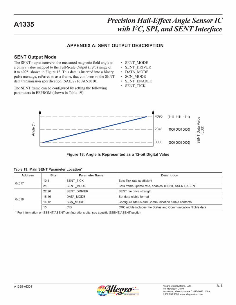
Precision Hall-Effect Angle Sensor ICwith I2C, SPI, and SENT InterfaceA1335
A-1Allegro MicroSystems, LLC115 Northeast CutoffWorcester, Massachusetts 01615-0036 U.S.A.1.508.853.5000; www.allegromicro.com
A1335-ADD1
0000
4095
2048
SE
NT
Da
ta V
alu
e(L
SB
)
(1111 1111 1111)
(0000 0000 0000)
(1000 0000 0000)
An
gle
(°)
Figure 18: Angle is Represented as a 12-bit Digital Value
The SENT output converts the measured magnetic field angle to a binary value mapped to the Full-Scale Output (FSO) range of 0 to 4095, shown in Figure 18. This data is inserted into a binary pulse message, referred to as a frame, that conforms to the SENT data transmission specification (SAEJ2716 JAN2010).
The SENT frame can be configured by setting the following parameters in EEPROM (shown in Table 19):
• SENT_MODE• SENT_DRIVER• DATA_MODE• SCN_MODE• SENT_ENABLE • SENT_TICK
SENT Output Mode
Table 19: Main SENT Parameter Location*Address Bits Parameter Name Description
0x31710:4 SENT_TICK Sets Tick rate coefficient
2:0 SENT_MODE Sets frame update rate, enables TSENT, SSENT, ASENT
0x319
22:20 SENT_DRIVER SENT pin drive strength
18:16 DATA_MODE Set data nibble format
14:12 SCN_MODE Configure Status and Communication nibble contents
15 CIS CRC nibble includes the Status and Communication Nibble data
* For information on SSENT/ASENT configurations bits, see specific SSENT/ASENT section
APPENDIX A: SENT OUTPUT DESCRIPTION

Precision Hall-Effect Angle Sensor ICwith I2C, SPI, and SENT InterfaceA1335
A-2Allegro MicroSystems, LLC115 Northeast CutoffWorcester, Massachusetts 01615-0036 U.S.A.1.508.853.5000; www.allegromicro.com
A1335-ADD1
The duration of a nibble is denominated in ticks. The period of a tick is set by the SENT_TICK parameter. The duration of the nibble is the sum of the low-voltage interval plus the high-voltage interval.
The parts of a SENT message are arranged in the following required sequence (see Figure 20):
1. Synchronization and Calibration: Flags the start of the SENT message.
2. Status and Communication Nibble: Provides A1335 status and the optional serial data determined by the setting of the SENT_SERIAL parameter.
3. Data: Angle information and optional data.4. CRC: Error checking.5. Pause Pulse (optional): Fill pulse between SENT message
frames.
MESSAGE STRUCTURE
Data within a SENT message frame is represented as a series of nibbles, with the following characteristics:
• Each nibble is an ordered pair of a low-voltage interval followed by a high-voltage interval
• The low-voltage interval acts as the delimiting state which acts as a boundary between each nibble. The length of this low-voltage interval is fixed at 5 ticks.
• The high-voltage interval performs the job of the information state and is variable in duration in order to contain the data payload of the nibble
• The slew rate of the falling edge may be adjusted using the SENT_DRIVER parameter.
Pause Pulse
(optional)CRC
tSENT
Data 6Data 1(MSB)
Status andCommun-
icationSynchronization and Calibration
12 to 27 ticks
12 to 27 ticks
12 to 27 ticks56 ticks
Nibble Name
SENT_FIXEDSENT_FIXED SENT_FIXEDSENT_FIXED SENT_FIXEDSENT_FIXED
12 to 27 ticks
Table 20: Nibble Composition and ValueQuantity of Ticks
Binary (4-bit) Value
Decimal Equivalent
ValueLow-
Voltage Interval
High- Voltage Interval
Total
5 7 12 0000 0
5 8 13 0001 1
5 9 14 0002 2
5 21 26 1110 14
5 22 27 1111 15
Ticks
0 5 12
MessageSignal
Voltage
LowInterval
HighInterval
Nibble Data Value = 0000
Ticks
0 5 27
MessageSignal
Voltage
LowInterval
HighInterval
Nibble Data Value = 1111
Figure 19: General Value Formation for SENT0000 (left), 1111 (right)
Figure 20: General Format for SENT Message Frame

Precision Hall-Effect Angle Sensor ICwith I2C, SPI, and SENT InterfaceA1335
A-3Allegro MicroSystems, LLC115 Northeast CutoffWorcester, Massachusetts 01615-0036 U.S.A.1.508.853.5000; www.allegromicro.com
A1335-ADD1
Synchronization and Calibration Pulse
The Synchronization and Calibration pulse is 56 ticks wide, mea-sured from falling-edge to falling edge, and delineates the start of a new message frame. The host microcontroller uses this pulse to rescale the subsequent nibble values to correct for clock variation between the controller and the sensor.
Status and Communication Nibble
The Status and Communication Nibble (SCN) provides diagnos-tic information along with other status and environmental data. Nibble contents are controlled via the SCN_MODE field within EEPROM. By default, contents of the SCN are not included in the 4 bit CRC at the end of each SENT frame. The CIS bit within EEPROM enables CRC coverage of the SCN contents. It should be noted that this option is not specified in the J2716 SENT stan-dard. With the CIS bit set the CRC is no longer compliant with that outlined in the SENT specification.
The SCN has three different types of bit values which may be present, depending on the SCN_MODE setting. These are:
a) Soft/Hard Error: Overall condition of the A1335, separated into Soft and Hard error flags. Detailed error information can be obtained via the expanded data nibbles, set via DATA_MODE, or through the slow serial communication.
SENT_FIXED SENT_FIXED SENT_FIXED SENT_FIXED SENT_FIXED SENT_FIXED
12 to 27 ticks 12 to 27 ticks 12 to 27 ticks 12 to 27 ticks56 ticks
Synchronizationand
Calibration
Statusand
Communication
Data 1(MSB) Data 6 CRC
PausePulse
(optional)
tSENT
Nibble Name
Figure 21: Synchronization and Calibration Pulse within the SENT Message Frame
SENT_FIXED SENT_FIXED SENT_FIXED SENT_FIXED SENT_FIXED SENT_FIXED
12 to 27 ticks 12 to 27 ticks 12 to 27 ticks 12 to 27 ticks56 ticks
Synchronizationand
Calibration
Statusand
Communication
Data 1(MSB) Data 6 CRC
PausePulse
(optional)
tSENT
Nibble Name
Figure 22: Status and Communication Nibble within the SENT Message Frame
Hard Error Flag:• Latched indefinitely if any of the following occur:
Watchdog Timeout
EEPROM hard error (multi-bit fault)
SRAM hard error
Self-test error
Any reset other than a POR or Hard/Soft reset
• Temporarily sets but clears after the following conditions pass:
Processor in “Idle Mode” (not generating new angle readings).
POR/Hard/Soft Reset
Soft Error Flag:• Latched temporarily, clears on next SENT frame unless
condition is still asserted.
Any unmasked errors asserted
Processor in “Idle Mode”
b) ID data: Die ID bits set via SA0 and SA1 pins. • ID[0]: Value set by the logic level of the SA0 pin.
• ID[1]: Value set by the logic level of the SA1 pin.
c) Serial Data: Two bits, consisting of the SerialSync and Seri-alData bits. Together they form the Short Serial Message (per J2716 Section 5.2.4.1).
• SerialSync: Indicates the start of a 16-bit serial message
• SerialData: Serial data, transmitted one bit at a time, MSB first.
Table 21: SCN Bit Contents
SCN_MODE
Bit 3 Bit 2 Bit 1 Bit 0
000 0 0 Soft Hard
001 SerialSync SerialData Soft Hard
010 ID[1] ID[0] Soft Hard
011 0 0 0 Soft+Hard
100 0 0 ID[1] ID[0]
101 SerialSync SerialData ID[1] ID[0]
110 Soft Hard ID[1] ID[0]
111 SerialSync SerialData 0 Soft+Hard

Precision Hall-Effect Angle Sensor ICwith I2C, SPI, and SENT InterfaceA1335
A-4Allegro MicroSystems, LLC115 Northeast CutoffWorcester, Massachusetts 01615-0036 U.S.A.1.508.853.5000; www.allegromicro.com
A1335-ADD1
Short Serial Message FormatThe SENT specification allows additional data transfer via spe-cific bits within the SCN. This data stream is also referred to as the “Slow Channel”.
The A1335 implements “Short Serial Message Format” as described in paragraph 5.2.4.1 of the SAE-J2716 specification. A 16-bit data packet is transmitted one bit at a time over consecu-tive SENT message frames, starting with the MSB. The begin-ning of each 16-bit packet is indicated by a “1” in the SerialSync bit. The message data is transmitted bit-by-bit via the SerialData bit. The 16-bit message packet is separated into 3 different fields:
a) Message ID (4 bits): Four leading bits of the serial data packet, used to identify data contents. Data rotates through the 16 message IDs as shown in Table 16. The Message ID may be considered the 4 LSB of a 12-bit alive counter that increments every 16 SENT frames
b) Message Data (8 bits): Eight bits of data.
c) CRC (4 bits): CRC checksum, used to validate the Message ID and Data. Same CRC algorithm as that used for the SENT message frame.
Sixteen separate SENT frames are needed to construct a complete 16-bit serial message. To transmit all 8 unique serial data mes-sages (Message ID 0-7) a total of 128 SENT transmission are necessary. 256 SENT transmissions are required for a complete rotation of the 16 message IDs.
SENT Data Nibbles:The 12-bit angle value is embedded in the first three data nibbles of every SENT frame and transmitted MSB first. Additional information may be transmitted by extending the number of data nibbles, up to 6. The contents and number of data nibbles in every SENT frame is configured using the DATA_MODE field in EEPROM.
Table 22: Short Serial Message Format in SENT Status and Communication Nibble
SNC Bit Nibble #1 2 3 4 5 6 7 8 9 10 11 12 13 14 15 16
SerialSync 1 0 0 0 0 0 0 0 0 0 0 0 0 0 0 0SerialData Message ID Data CRC
Table 23: Serial Output DataMessage ID
(4 bits) Data (8 bits)
0 (8) 8-bit Alive counter (increments by one, every 0-15 rotation of the Message ID field))
1 (9) Temperature in degrees Celsius, offset by +64 (subtract 64 to get measured temperature)
2(10) Magnetic field reading in gauss, divided by 8 (multiply by 8 to obtain gauss rating)
3 (11) STATUS, bits [23:16] See Table 19.
4 (12) STATUS, bits [15:8] See Table 19.
5 (13) STATUS, bits [7:0] See Table 19.
6 (14) First byte of the customer programmable field1
7 (15) Second byte of customer programmable field2
1 The most significant 4 bits correspond to EEPROM register 0x307, bits [23:20]. The least significant 4 bits correspond to EEPROM register 0x317, bits [23:20].2 Corresponds to EEPROM register 0x317, bits [19:12].
SENT_FIXED SENT_FIXED SENT_FIXED SENT_FIXED SENT_FIXED SENT_FIXED
12 to 27 ticks 12 to 27 ticks 12 to 27 ticks 12 to 27 ticks56 ticks
Synchronizationand
Calibration
Statusand
Communication
Data 1(MSB) Data 6 CRC
PausePulse
(optional)
tSENT
Nibble Name
Figure 23: SENT Data Nibbles within the SENT Message Frame

Precision Hall-Effect Angle Sensor ICwith I2C, SPI, and SENT InterfaceA1335
A-5Allegro MicroSystems, LLC115 Northeast CutoffWorcester, Massachusetts 01615-0036 U.S.A.1.508.853.5000; www.allegromicro.com
A1335-ADD1
DATA_MODE = 0002 (0)
Data Nibble 1,2,3 = Angle1 2 3
Angle Reading
DATA_MODE = 0012 (1)
Data Nibble 1,2,3 = Angle Data Nibble 4,5 = 8-bit Alive Counter Data Nibble 6 = 1s complement of Data Nibble 1
1 42 53 6
Angle Reading ~Angle[11:8]Alive[7:0]
Wraps every
256 frames.
When combined with SCN_MODE = 3, this implements the “Single Secure Sensor” requirement outlined in SAE-J2716 Appendix A.
DATA_MODE = 0102 (2)
Data Nibble 1,2,3 = AngleData Nibbles 4 = Message ID (see Short Serial Output)Data Nibbles 5,6 = Rotating Extended Data (see Short Serial Output)
1 42 53 6
Angle Reading Status
(rotates between upper and
lower 12 bits)
Status bits rotate between upper and lower 12 bits of the SENT status flag, distinguished by the LSB. For the upper 12 bits the LSB always equals 1. For the lower 12 bits the LSB always equals 0.See description of SENT status flags.
DATA_MODE = 0112 (3)
Data Nibble 1,2,3 = AngleData Nibbles 4,5,6 = Rotating Extended Data, same sequence as Serial Message.
1 42 53 6
Angle Reading Rotating ExData
(Follows Serial Data)
Message
ID
Nibbles 4,5,6 make up a rotating serial data stream following the same rotation pattern as the short serial message transmission. Allows one 12-bit packet (4 bits for ID, 8 bits for data) to be transmitted every SENT frame. Provides a faster method of obtaining extra sensor information normally supplied via the slow serial transmission.
DATA_MODE = 1002 (4) and 1012 (5)
Data Nibble 1,2,3 = AngleData Nibble 4 = Self Test flag and ID
1 42 3
Angle Reading ST & ID
Nibble 4 provides a self-test failure flag as well as the two address bits set via the SA0 and SA1 pins.
DATA_MODE = 1102 (6)
Data Nibble 1,2,3 = AngleData Nibble 4,5 = Rotating Status Bits (2 MSB identify quadrant)Data Nibble 6 = Self Test flag and ID
1 42 53 6
Angle Reading Status
Complete rotation
every 4 frames.
ST & ID
Nibbles 4,5 rotate through the 24 status flags, six bits at a time. The two MSB of nibble 4 serve as a counter differentiating each of the four status blocks (shown in Table 19).Nibble 6 provides a self-test failure flag, as well as the two ID bits set via SA0 and SA1 pins
DATA_MODE = 1112 (7)Data Nibble 1,2,3 = AngleData Nibbles 4,5 = Rotating Extended Data. Same sequence as serial messageData Nibble 6 = Self Test flag and ID
ST & IDAngle Reading ExtData
Rotates
Data
ID
1 42 53 6
Nibbles 4,5 make up a rotating serial data stream following the same rotation pattern as the short serial message transmission. LSB of Data_ID indicates if ExtData is upper nibble(1) or lower nibble(0), of the 8-bit data field. Three MSB of Data_ID indicates data type (maps to Message ID 0 -7)Nibble 6 provides a self-test failure flag, as well as the two ID bits set via SA0 and SA1 pins
SENT Data Mode Options

Precision Hall-Effect Angle Sensor ICwith I2C, SPI, and SENT InterfaceA1335
A-6Allegro MicroSystems, LLC115 Northeast CutoffWorcester, Massachusetts 01615-0036 U.S.A.1.508.853.5000; www.allegromicro.com
A1335-ADD1
Self-Test and ID NibbleThe Self-Test and ID (ST&ID) nibble is optional. It is included as one of the extended nibbles when using DATA_MODEs 4-7. This nibble consists of three data bits (MSB is always 0), shown below:
The ST bit, indicates a failure of one of the three internal self-tests (CVH self-test, ROM BIST, RAM BIST). If set, this indicates significant failure of the sensor, and a reset should be initiated.
ID[0] and ID[1] provide the sensor ID value as determined via the logic values of the SA0 and SA1 pins.
This nibble is particularly useful when sharing SENT lines and using DATA_MODE 4 or 5, as it allows the Self-Test diagnostic results and corresponding sensor ID to be quickly determined without a significant latency penalty (only one nibble to the SENT frame).
SENT Status Bit DescriptionThe A1335’s extensive status and error flags may be read at any time via I2C or SPI protocols, or by entering Manchester Com-munication Mode. To facilitate error/status flag reporting by way of the unidirectional SENT protocol, a selection of these flags are communicated via extra data nibbles when using DATA_MODEs 2 or 6. These status flags are also transmitted via the slow serial protocol through the SCN.
The flags are 0 if the condition is clear and 1 if the condition is true. For transient conditions, the flag will clear after the bit is presented on the SENT output.
0
Bit 3
ST
Bit 2
ID[1]
Bit 1
ID[0]
Bit 0
Figure 24: ST & ID Nibble
Table 24: SENT Status Flag DefinitionsBit Status Flag Name Symbol Definition23 Reserved R Always 0
22 Reset other than POR SF21
21 SRAM Hard Error SF20 Uncorrectable SRAM fault
20 EEPROM Hard Error SF19 Uncorrectable EEPROM fault
19 PC Watchdog SF18 Microprocessor halted
18 Watchdog timer SF17 Microprocessor locked up
17 Self-Test Error SF16 Asserts if any one of the three internal self-tests fails
16 Angle Timeout SF15 No angle updated within expected time. May occur with no magnet present.
15 Temperature Out of Range SF14
14 Idle Mode SF13 Microprocessor is not updating angle content (in idle or booting/self-test).
13 POR SF12 Power-on reset
12 Reserved R Always (1) when using DATA_MODE 2; indicates upper 12 bits. Always (0) during Serial transmission or when using DATA_MODE 6.
11 SRAM Soft Error SF11 Correctable SRAM error
10 EEPROM Softerror SF10 Correctable EEPROM error
9 Interface Error SF09 SPI, Manchester checksum/bit detect error, SENT contention/slot error
8 Access Error SF08 Extended error, memory access error, extended overflow
7 Angle Warning SF07 IIR filter reset, angle slippage (computation too long for ORATE setting), gain overflow (short stroke)
6 Angle High SF06 Short stroke only
5 Angle Low SF05 Short stroke only
4 Magnetic Field High SF04
3 Magnetic Field Low SF03 Default of 100 G
2 Overvoltage SF02
1 Undervoltage SF01
0 Reserved R Always 0. Indicates lower 12 bits.

Precision Hall-Effect Angle Sensor ICwith I2C, SPI, and SENT InterfaceA1335
A-7Allegro MicroSystems, LLC115 Northeast CutoffWorcester, Massachusetts 01615-0036 U.S.A.1.508.853.5000; www.allegromicro.com
A1335-ADD1
Status Flag Locations for SENT DATA_MODE 2 (over 2 SENT frames)Nibble1 Nibble2 Nibble3 Nibble4 Nibble5 Nibble6A[11:8] A[7:4] A[3:0] SF11 SF10 SF09 SF08 SF07 SF06 SF05 SF04 SF03 SF02 SF01 R (0)
Status Flag Locations for SENT DATA_MODE 6 (over 4 SENT frames)Nibble1 Nibble2 Nibble3 Nibble4 Nibble5 Nibble6A[11:8] A[7:4] A[3:0] 0 0 SF05 SF04 SF03 SF02 SF01 R (0) ST & ID
Nibble1 Nibble2 Nibble3 Nibble4 Nibble5 Nibble6A[11:8] A[7:4] A[3:0] 0 1 SF11 SF10 SF09 SF08 SF07 SF06 ST & ID
Nibble1 Nibble2 Nibble3 Nibble4 Nibble5 Nibble6A[11:8] A[7:4] A[3:0] R (0) SF21 SF20 SF19 SF18 SF17 SF16 SF15 SF14 SF13 SF12 R (1)
Nibble1 Nibble2 Nibble3 Nibble4 Nibble5 Nibble6A[11:8] A[7:4] A[3:0] 1 0 SF16 SF15 SF14 SF13 SF12 R (0) ST & ID
Nibble1 Nibble2 Nibble3 Nibble4 Nibble5 Nibble6A[11:8] A[7:4] A[3:0] 1 1 R (0) SF21 SF20 SF19 SF18 SF17 ST & ID

Precision Hall-Effect Angle Sensor ICwith I2C, SPI, and SENT InterfaceA1335
A-8Allegro MicroSystems, LLC115 Northeast CutoffWorcester, Massachusetts 01615-0036 U.S.A.1.508.853.5000; www.allegromicro.com
A1335-ADD1
SENT CRC NibbleThe CRC nibble is a 4-bit error checking code, implemented per the SAE-J2716 SENT “recommended” specification.
The CRC is calculated using the polynomial x4 + x3 + x2 + 1, initialized to 0101.
By default, the checksum covers only the contents of the data nibbles (3-6 nibbles). By setting the CIS bit within EEPROM, the contents of the SCN are included within the CRC nibble.
SENT Pause Pulse (Optional)The Pause Pulse is an optional addition to the SENT message frame, transmitted following the CRC nibble. It acts to “fill-in” the frame until the beginning of the next SENT transmission.
The pulse may behave in one of two ways, based on the SENT_MODE setting.
With SENT_MODE set to 2, a Pause Pulse will be inserted until new angle data is available. The inserted Pause Pulse is a minimum of 12 Ticks in length. If a pause longer than 768 Ticks is required, the pulse will restart requiring a minimum of 12 more Ticks.
For SENT_MODE values greater than 3-7, the sensor operates in either triggered or addressable/sequential SENT mode. In these modes the sensor outputs a SENT message frame in response to host action (either a trigger or a function pulse). When not responding to the host the sensor will output a Pause Pulse of indefinite length (i.e. remains high until host a host request).
SENT_FIXED SENT_FIXED SENT_FIXED SENT_FIXED SENT_FIXED SENT_FIXED
12 to 27 ticks 12 to 27 ticks 12 to 27 ticks 12 to 27 ticks56 ticks
Synchronizationand
Calibration
Statusand
Communication
Data 1(MSB) Data 6 CRC
PausePulse
(optional)
tSENT
Nibble Name
Figure 25: CRC Nibble within the SENT Message Frame
SENT_FIXED SENT_FIXED SENT_FIXED SENT_FIXED SENT_FIXED SENT_FIXED
12 to 27 ticks 12 to 27 ticks 12 to 27 ticks 12 to 27 ticks56 ticks
Synchronizationand
Calibration
Statusand
Communication
Data 1(MSB) Data 6 CRC
PausePulse
(optional)
tSENT
Nibble Name
Figure 26: Pause Pulse within the SENT Message Frame
Low
Low Low (host)
7 to 763 Ticks
Infinite (until pulled low by host)
5 Ticks
5 Ticks Minimum 1.8 µs
High
High
SENT_MODE 2
SENT_MODEs3 through 7
Low5 Ticks 7 to 763 Ticks
High
Figure 27: SENT Pause Pulse

Precision Hall-Effect Angle Sensor ICwith I2C, SPI, and SENT InterfaceA1335
A-9Allegro MicroSystems, LLC115 Northeast CutoffWorcester, Massachusetts 01615-0036 U.S.A.1.508.853.5000; www.allegromicro.com
A1335-ADD1
The timing and method of SENT transmission may be configured using the SENT_MODE field within EEPROM. The method of SENT transmission falls within the following three categories:
1. Free Running SENT Angle information is automatically placed on the SENT line with no prompting from the host. Depending on settings, the SENT message frames may be transmitted back-to-back, or synchronized with each update of the angle value.
2. Triggered SENT (TSENT)
A SENT message frame occurs only when initiated by the host. The A1335 sensor will output a continuous Pause pulse, during this the host triggers a SENT frame by pulling the SENT line low for a minimum of TTrig(MIN). Once released the sensor responds with a SENT message frame
3. Shared SENT Two distinct formats. Sequential SENT (SSENT) and Addressable SENT (ASENT). Allow sharing a single SENT line amongst four compatible devices
SENT_MODE Visual Description0002 (0) – SENT disabled.
0012 (1) SENTmessage
SENT message 1 SENT message 2
TSENT1 TSENT2
syn
c
syn
c
da
ta
da
ta
SC
N
SC
N
CR
C
CR
C Streaming output with variable message duration and no pause pulse. Angle data is sampled near the end of the Status and Communication nibble. Maximum age at time of sampling is 2ORATE × 32 µs. Depending on Tick time and ORATE setting, same data may be transmitted multiple times. This mode provides the quickest data delivery rate
0102 (2) SENTmessage
SENT message 1 SENT message 2
12TicksMin
syn
c
pa
use
pa
use
da
ta
SC
N
CR
C
syn
c
da
ta
SC
N
SENT message frames are synchronized with the device internal update rate. Pause pulse is inserted until fresh data becomes available. Angle data is sampled between 1 to 2 Tick times of the Synchronization pulse. Pause pulse varies in length between 12 to 2ORATE × 32 µs (Pulse will restart after 768 ticks).
0112 (3)
(previous message)
Controller pulls OUT low
SENT message
Waiting
period, twait sync
pause
pause
data
SC
N
CR
C
sync
Controller releases OUT
Sensor IC starts message
Angle data latched
t (7 ticks)dSENT
TSENT SCN sampling:Controller initiates a SENT transmission by pulling the line low, during a Pause Pulse. When the controller releases the output, after a delay of tdSENT the SENT message begins. Angle data is latched at the end of the SCN. Data age may be up to 2ORATE × 32 µs when latched.This option is useful when the controller requires a prompt with minimum “age” of the angle data.
1002 (4)
(previous message)
Controller pulls OUT low;angle data latched
SENT message
Waiting
period, twait sync
pause
pause
data
SC
N
CR
C
Controller releases OUT
Sensor IC starts message
t (7 ticks)dSENTTSENT Falling edge sampling:Similar to SENT_MODE = 3, except angle data is latched once the output line is pulled low.Useful when multiple ICs are connected to a single controller. Allows synchronous sampled data to be retrieved one device at a time, by releasing the trigger for each individual sensor.
1012 (5) – Addressable SENT (ASENT). See Shared SENT section
1102 (6) – Sequential SENT (SSENT). See Shared SENT Section.
1112 (7) – Long Sequential SENT. See Shared SENT Section.
SENT OUTPUT MODE

Precision Hall-Effect Angle Sensor ICwith I2C, SPI, and SENT InterfaceA1335
A-10Allegro MicroSystems, LLC115 Northeast CutoffWorcester, Massachusetts 01615-0036 U.S.A.1.508.853.5000; www.allegromicro.com
A1335-ADD1
SHARED SENT PROTOCOLAddressable SENT (ASENT) and Sequential SENT (SSENT) are extensions of the Allegro Triggered SENT (TSENT) protocol. ASENT and SSENT allow multiple Allegro sensors with SENT output capability to co-exist on a single shared SENT bus. The Host (ECU) is able to select one sensor at a time, addressing that sensor to respond with a SENT output packet, and thus poll each sensor on the bus over some period of time.
ASENT and SSENT, like Triggered SENT, require an open-drain system configuration, in which any sensor, or the Host, can pull the SENT line low. The SENT line is pulled high by an external resistor to a known VCC. A high level is attainable on the bus only when no device is actively pulling the line low.
In ASENT and SSENT, each sensor on the bus is assigned a unique SensorID number between 0 and 3, allowing up to 4 Sen-sors to co-exist on the bus. This SensorID number is assigned by the logic state of the SA0 and SA1 pins.
Function Pulses
This section describes the different function pulses that are refer-enced later during the ASENT and SSENT section.
The host communicates to a sensor or sensors via different Func-tion Pulses, which are equivalent in nature to a TSENT trigger pulse, but with defined widths. A Function Pulse is placed on the SENT bus by the Host pulling the SENT line low for a defined number of Ticks greater than a normal SENT pulse low period.
The duration of the low time is measured by the Sensors and interpreted as a designated Function.
Functions that are acted upon by all sensors simultaneously are
designated Broadcast Pulses. Functions that are acted upon by only one sensor are designated Addressing Pulses and are associ-ated with a target sensor ID. A Function Pulse may be defined as both a Broadcast and an Addressing pulse. For instance, all sensors will sample and hold data, but only one will transmit a SENT packet.
A sensor that does not support a specific function will not respond to the Function Pulse.
Function Pulses must be greater in duration than the SENT pulse low time (5 Ticks on the A1335) to not be mistaken as a part of a normal SENT transmission
The duration of Function Pulses are defined in SENT Ticks in order to scale with the SENT frame itself. Min and Max pulse durations are set such that they satisfy electrical and timing char-acteristics.
The various Function Pulses with their expected Tick ranges are shown in Table 25 through Table 27.
SensorID = 0
SensorID = 1
SensorID = 2
SensorID = 3
Host(ECU)
VCC 5 V Max
R
C
Bus Capacitance
Figure 28: Shared SENT Bus Example
FunctionPulse
Greater than 7 Ticks LowWidth Defines Function
Figure 29: Function Pulse (Output by Host)

Precision Hall-Effect Angle Sensor ICwith I2C, SPI, and SENT InterfaceA1335
A-11Allegro MicroSystems, LLC115 Northeast CutoffWorcester, Massachusetts 01615-0036 U.S.A.1.508.853.5000; www.allegromicro.com
A1335-ADD1
Table 25: ASENT Functional PulsesFunction Type Related Options Min Tick Nom Tick Max Tick Description
F_OUTPUT Addressing/Broadcast NO_SAMPLE 15 17 19
Addressed Sensor responds with SENT frame, containing either held data (from F_SAMPLE) or current data.
F_SAMPLE Addressing/Broadcast
NO_FSAMPLE SAMPLE_ADR 31 35 39
Sensors sample and hold their magnetic data, unless NO_FSAMPLE=1. If SAMPLE_ADR=1, this is also an AddressingPulse, and addressed Sensor responds with SENT frame.
F_DIAG Addressing/Broadcast
DIAG_ADR DIAG_ENABLE 56 63 70 Sensor(s) enter Diagnostics as described in User-
Initiated Diagnostic Support.
Table 26: SSENT Functional Pulses. SENT_MODE = 6Function Type Related Options Min Tick Nom Tick Max Tick Description
F_OUTPUT Addressing/Broadcast
NO_SAMPLEZERO_SAMPLE 15 17 19
Addressed Sensor responds with SENT frame, containing either held data (from Slot 0 sampling or F_SAMPLE) or current data. If ZERO_SAMPLING=1 and Slot=0, Sensors will sample-and-hold their magnetic data.
F_SAMPLE Addressing/Broadcast
NO_FSAMPLE SAMPLE_ADR 31 35 39
Sensors sample and hold their magnetic data, unless NO_FSAMPLE=1.If SAMPLE_ADR=1, this is also an Addressing Pulse, and addressed Sensor responds with SENT frame.
F_DIAG Addressing/Broadcast
DIAG_ADR DIAG_ENABLE 56 63 70 Sensor(s) enter Diagnostics as described in User-
Initiated Diagnostic Support.
F_SYNC Broadcast 93 104 115 All sensors synchronize their Slot Counters such that the next Slot is for Sensor ID 0.
Table 27: Long SSENT Functional Pulses. SENT_MODE = 7Function Type Related Options Min Tick Nom Tick Max Tick Description
F_OUTPUT Addressing/Broadcast
NO_SAMPLEZERO_SAMPLE 9
Per micro controller
spec81
Addressed Sensor responds with SENT frame, containing either held data (from Slot 0 sampling) or current data. If ZERO_SAMPLING=1 and Slot=0, Sensors will sample-and-hold their magnetic data.
F_SYNC Broadcast 105 140 171 All sensors synchronize their Slot Counters such that the next Slot is for Sensor ID 0.
F_DIAG Addressing/Broadcast
DIAG_ADR DIAG_ENABLE 216 240 264 Sensor(s) enter Diagnostics as described in User-
Initiated Diagnostic Support.

Precision Hall-Effect Angle Sensor ICwith I2C, SPI, and SENT InterfaceA1335
A-12Allegro MicroSystems, LLC115 Northeast CutoffWorcester, Massachusetts 01615-0036 U.S.A.1.508.853.5000; www.allegromicro.com
A1335-ADD1
SEQUENTIAL SENT (SSENT)
SSENT Addressing ProtocolThe SSENT protocol requires Sensors on the bus to be polled in sequential order, meaning increasing, consecutive and rotating order by Sensor ID starting with Sensor ID 0. The Slot for a Sen- sor is the time at which that Sensor is expected to respond to an Addressing Pulse and other Sensors are expected to not respond.
Each Sensor independently maintains a Slot Counter that is incre-mented each time the Sensor detects an Addressing Pulse. This Slot Counter becomes the Slot Number, which is used by the Sen-sor to decide which Sensor is being polled by the Host. The Slot Counter is compared to the Sensor ID, and if they match, that Sensor responds with the SENT Frame, and all other Sensors do not respond, although they increment their own Slot Counter.
If the Slot Counter is incremented past the total number of Sen-sors on the bus (MAX_SENSOR option), the Slot Counter is returned to 0. Each Sensor must be programmed consistently with the total number of Sensors so they all roll over to 0 at the same count. Sensors do not increment their Slot Counter on a Broad-cast Pulse.
The SSENT protocol relies on each Sensor maintaining the exact same Slot Number by counting the Addressing Pulses. In order to synchronize all Sensors to the same Slot Number, the SSENT protocol has a broadcast F_SYNC pulse that is used by the Host
to force all Sensors to reset their SlotCounter to 0.
Long SSENT (SENT_MODE = 7) allows the A1335 to work with existing shared SENT methodologies. The added overhead decreases the rate at which messages may be transmitted.
In order to reduce the burden on the Host, and also to improve detection and recovery from BusContention or system errors affecting the SENT bus, the SSENT protocol has the following Configuration Options that can be selected.
• SLOT_MARKING. When enabled, each Sensor will wait a different length of time following an Addressing Pulse, based on their Sensor ID. This leaves the SENT bus in a high state for a varying duration before the Sensor pulls the line low to begin the SENT Frame. All Sensors on the bus (including the addressed Sensor) measure this time to interpret the Sensor ID of the transmitting sensor. By comparing this to the Slot Counter, each Sensor can recognize if an unexpected Sensor responded to the Addressing Pulse. By default, the Sensor would then drop Offline, since it cannot be known which Sensor is out-of-sync. This Option increases the overhead on the bus and therefore reduces the maximum rate at which Sensors can be polled. SlotMarking increases the polling time of a Sensor by the Slot Marking time for that Sensor. All sensors on a bus must be configured with the same choice for this option.
Delay (Sensor)FrameReqPulse (Host) SENT Frame (Sensor)
SlotNumber N
BusIdle
Greater than 7 Ticks LowWidth Defines Function
Sensors Increment Slot Counter
Delay7 Ticks or
SlotMarking
Sensor Responds ifSensorID = SlotNumber
Figure 30: SSENT Sensor Addressing
F_SYNC (Host) BusIdle
BusIdle
BusIdle
BusIdle
BusIdle
BusIdle
BusIdle
BusIdle
FrameReq
FrameReq
FrameReq
FrameReq
Dly
Dly
Dly
Dly
SENT Frame SensorID 0 (Slot 0)
SENT Frame SensorID 1 (Slot 1)
SENT Frame SensorID 2 (Slot 2)
SENT Frame SensorID 0 (Slot 0)
Figure 31: SSENT Sensor Addressing – No Slot Marking (3 Sensors on Bus)

Precision Hall-Effect Angle Sensor ICwith I2C, SPI, and SENT InterfaceA1335
A-13Allegro MicroSystems, LLC115 Northeast CutoffWorcester, Massachusetts 01615-0036 U.S.A.1.508.853.5000; www.allegromicro.com
A1335-ADD1
F_SYNC (Host) BusIdle
BusIdle
BusIdle
BusIdle
BusIdle
BusIdle
BusIdle
BusIdle
FrameReq
FrameReq
FrameReq
FrameReq
Dly
DlySlot1
DlySlot2
DlySlot3
SENT Frame SensorID 0 (Slot 0)
SENT Frame SensorID 1 (Slot 1)
SENT Frame SensorID 2 (Slot 2)
SENT Frame SensorID 3 (Slot 3)
BusIdle BusIdleFrameReq Dly SENT Frame SensorID 0 (Slot 0)
Figure 32: SSENT Sensor Addressing – With Slot Marking (4 Sensors on Bus)
• POR_OFFLINE. When enabled, a Sensor will stay Offline until the Host issues F_SYNC, or one of the other synchronization options takes effect (C_IDLE_SYNC). If disabled, a Sensor will power-up with its SlotCounter set to 0, and will go directly Online. This allows the Sensors to initialize without any Host interaction. However, if a Sensor gets power-on-reset after the bus is in operation, its counter may be out-of-sync with other Sensors, and this could result in bus contention.
• IDLE_SYNC. When enabled, a Sensor will monitor the bus for a long high (BusIdle) period greater than 510 ticks and reset its Slot Counter to 0. This option could be used if Sensor polling is expected to always be periodic and continuous, such that the only extended BusIdle time would be after power-up.
SSENT FUNCTION PULSES
• F_OUTPUT: Addressed sensor will return a SENT frame with sampled magnetic data. If there is data from a sample- and-hold operation available (F_SAMPLE or via C_ZERO_ SAMPLE=1), then that data is returned, otherwise current data is sampled and returned. A Sensor configured with C_ZERO_SAMPLE=1 will sample-and-hold on the rising edge of the F_OUTPUT pulse for Slot 0. A Sensor configured
with C_NO_SAMPLE=1 and C_ZERO_SAMPLE=0 will never sample-and-hold, so will always return current data in response to F_OUTPUT.
• F_SAMPLE: All sensors except those configured for NO_SAMPLE=1 will sample and hold their data at the rising edge of the pulse. If SAMPLE_ADR=0, this is a BroadcastPulse to a Sensor, and that Sensor will not respond. If SAMPLE_ ADR=1, this is also an AddressingPulse to a Sensor, and the addressed sensor will return a SENT frame with either the sampled or current data. The SAMPLE_ADR must be configured the same for all parts on the bus.
• F_DIAG: Sensor(s) will enter self-test Diagnostics based on DIAG_ENABLE and DIAG_ADR options. If configured with DIAG_ADR=0, the Sensor treats F_DIAG as a BroadcastPulse, does not respond, and immediately enters Diagnostics unless DIAG_ENABLE=0. If configured with DIAG_ADR=1, the Sensor treats F_DIAG as an Addressing Pulse. The addressed Sensor does not respond, but enters diagnostics if DIAG_ENABLE=1.
• F_SYNC: All Sensors will synchronize their Slot Numbers by setting their Slot Counters such that the next Addressing Pulse is for Slot 0.
Table 28: Slot Marking Delay TimeSensor ID Delay Time in Ticks (Nominal)
0 7*
1 18*
2 36*
3 62*
* Delay time not intended for use by host. Tick values are approximate and will differ from part to part due to oscillator variance.

Precision Hall-Effect Angle Sensor ICwith I2C, SPI, and SENT InterfaceA1335
A-14Allegro MicroSystems, LLC115 Northeast CutoffWorcester, Massachusetts 01615-0036 U.S.A.1.508.853.5000; www.allegromicro.com
A1335-ADD1
ADDRESSABLE SENT (ASENT)
ASENT Addressing ProtocolThe ASENT protocol allows Sensors to be polled in an arbitrary order. The Sensor ID is transmitted by the Host following any AddressingPulse as a series of 0, 1, 2, or 3 IncAdrPulses. After this sequence, the SENT line is left in a high state, and each sen-sor will recognize after a time period of about 18 nominal TICKs that there are no more IncAdrPulses coming. The sensor whose ID matches the number of IncAdrPulses received will respond.
ASENT Function Pulses• F_OUTPUT: Addressed sensor will return a SENT frame
with sampled magnetic data. If there is data available from a sample-and-hold operation (F_SAMPLE), then that data is returned, otherwise current data is sampled and returned. A Sensor configured with NO_SAMPLE=1 will not sample- and-hold, so will always return current data in response to F_OUTPUT.
• F_SAMPLE: All sensors except those configured for NO_ SAMPLE=1 will sample and hold their data at the rising edge
of the pulse. If SAMPLE_ADR=0, this is a BroadcastPulse to a Sensor, and that Sensor will not respond. If SAMPLE_ADR=1, this is also an AddressingPulse to a Sensor, and the addressed sensor will return a SENT frame with either the sampled or current data. The SAMPLE_ADR must be configured the same for all parts on the bus.
• F_DIAG: Sensor(s) will enter self-test Diagnostics based on C_DIAG_ENABLE and C_DIAG_ADR options. If configured with DIAG_ADR=0, the Sensor treats F_DIAG as a BroadcastPulse, does not respond, and immediately enters Diagnostics unless DIAG_ENABLE=0. If configured with DIAG_ADR=1, the Sensor treats F_DIAG as an AddressingPulse. The addressed Sensor does not respond, but enters diagnostics if DIAG_ENABLE=1.
ASENT Host Requirements:• The Host must initiate SENT frame output by selecting
appropriate Function pulses.
• The Host must detect timeouts or SENT frame contention following any Function pulse, and take appropriate recover action.
IncAdrPulse
7 Ticks High 5 Ticks Low
Figure 33: ASENT IncAdrPulse (Output by Host)

Precision Hall-Effect Angle Sensor ICwith I2C, SPI, and SENT InterfaceA1335
A-15Allegro MicroSystems, LLC115 Northeast CutoffWorcester, Massachusetts 01615-0036 U.S.A.1.508.853.5000; www.allegromicro.com
A1335-ADD1
IncAdrPulses (0-3)(Host)
IncAdr
IncAdr IncAdr
IncAdr IncAdr IncAdr
FrameReqPulse (Host)
FrameReqPulse (Host)
FrameReqPulse (Host)
FrameReqPulse (Host)
FrameReqPulse (Host)
SENT Frame (Sensor)
SENT Frame (Sensor)
SENT Frame (Sensor)
SENT Frame (Sensor)
SENT Frame (Sensor)
EndAddress > 18 Ticks High
EndAddress
EndAddress
EndAddress
EndAddress
BusIdle
BusIdle
BusIdle
BusIdle
Greater than 8 Ticks LowWidth Defines Function
SensorID 0 Selected
Host Adds Pulses forSensorIDs 1, 2, or 3
Sensor Recognizes the Endof the Addressing Phrase
Addressed SensorResponds
SensorID 0
SensorID 1
SensorID 2
SensorID 3
Figure 34: ASENT Sensor Addressing
SENSOR MAGNETIC DATA SAMPLING
Sensors sample their magnetic data based on a combination of FunctionPulse and configuration options. There are two types of sampling supported: SampleOnOutput and SampleAndHold.
SampleOnOutput:SampleOnOutput is when the Sensor samples magnetic data within a short time period preceding the transmission of that data in the SENT frame. This provides the Host with a minimal latency between the data sample and its reception at the Host. The sensor uses SampleOnOutput in the following cases:
• An F_OUTPUT function is addressed to that sensor and no held data is present.
SampleAndHoldSampleAndHold is when the Sensor samples magnetic data on the rising edge of a specific FunctionPulse and holds it for output in a SENT frame later in time, when addressed. This allows the data sampling from multiple sensors to be synchronized, with the tradeoff in latency. The sensor does a SampleAndHold of its magnetic data in the following cases:
• An F_SAMPLE function is broadcast, unless the sensor is configured with NO_FSAMPLE = 1.
• The Host initiates an F_OUTPUT function in SSENT mode, the SlotNumber is for Sensor ID 0, and the sensor is configured with ZERO_SAMPLE = 1.
Once the Sensor has data held from a SampleAndHold, it trans-mits it in the SENT frame the next time it is addressed. If the sensor is again polled before another SampleAndHold, then that Sensor will return the same data unless certain events intervene, in which case the SampleAndHold data is discarded. These events are:
• A diagnostic is executed that prevents the SENT interface from obtaining valid magnetic data from the sensors logic (CVH_SelfTest).
• The SENT interface is disabled, for instance the SENT line is taken over by the receipt of a Manchester Access Code.
F_OUTPUT + Addressing SyncPulse ScnNibble DataNibble
AngleSampled Here
Figure 35: SampleOnOutput Example
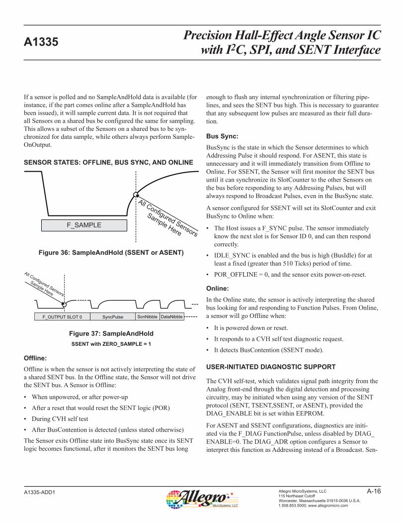
Precision Hall-Effect Angle Sensor ICwith I2C, SPI, and SENT InterfaceA1335
A-16Allegro MicroSystems, LLC115 Northeast CutoffWorcester, Massachusetts 01615-0036 U.S.A.1.508.853.5000; www.allegromicro.com
A1335-ADD1
If a sensor is polled and no SampleAndHold data is available (for instance, if the part comes online after a SampleAndHold has been issued), it will sample current data. It is not required that all Sensors on a shared bus be configured the same for sampling. This allows a subset of the Sensors on a shared bus to be syn-chronized for data sample, while others always perform Sample-OnOutput.
SENSOR STATES: OFFLINE, BUS SYNC, AND ONLINE
Offline:Offline is when the sensor is not actively interpreting the state of a shared SENT bus. In the Offline state, the Sensor will not drive the SENT bus. A Sensor is Offline:
• When unpowered, or after power-up
• After a reset that would reset the SENT logic (POR)
• During CVH self test
• After BusContention is detected (unless stated otherwise)
The Sensor exits Offline state into BusSync state once its SENT logic becomes functional, after it monitors the SENT bus long
enough to flush any internal synchronization or filtering pipe-lines, and sees the SENT bus high. This is necessary to guarantee that any subsequent low pulses are measured as their full dura-tion.
Bus Sync:BusSync is the state in which the Sensor determines to which Addressing Pulse it should respond. For ASENT, this state is unnecessary and it will immediately transition from Offline to Online. For SSENT, the Sensor will first monitor the SENT bus until it can synchronize its SlotCounter to the other Sensors on the bus before responding to any Addressing Pulses, but will always respond to Broadcast Pulses, even in the BusSync state.
A sensor configured for SSENT will set its SlotCounter and exit BusSync to Online when:
• The Host issues a F_SYNC pulse. The sensor immediately know the next slot is for Sensor ID 0, and can then respond correctly.
• IDLE_SYNC is enabled and the bus is high (BusIdle) for at least a fixed (greater than 510 Ticks) period of time.
• POR_OFFLINE = 0, and the sensor exits power-on-reset.
Online:In the Online state, the sensor is actively interpreting the shared bus looking for and responding to Function Pulses. From Online, a sensor will go Offline when:
• It is powered down or reset.
• It responds to a CVH self test diagnostic request.
• It detects BusContention (SSENT mode).
USER-INITIATED DIAGNOSTIC SUPPORT
The CVH self-test, which validates signal path integrity from the Analog front-end through the digital detection and processing circuitry, may be initiated when using any version of the SENT protocol (SENT, TSENT,SSENT, or ASENT), provided the DIAG_ENABLE bit is set within EEPROM.
For ASENT and SSENT configurations, diagnostics are initi-ated via the F_DIAG FunctionPulse, unless disabled by DIAG_ENABLE=0. The DIAG_ADR option configures a Sensor to interpret this function as Addressing instead of a Broadcast. Sen-
F_SAMPLE
All Configured Sensors
Sample Here
Figure 36: SampleAndHold (SSENT or ASENT)
F_OUTPUT SLOT 0 SyncPulse ScnNibble DataNibble
All Configured Sensors
Sample Here
Figure 37: SampleAndHoldSSENT with ZERO_SAMPLE = 1

Precision Hall-Effect Angle Sensor ICwith I2C, SPI, and SENT InterfaceA1335
A-17Allegro MicroSystems, LLC115 Northeast CutoffWorcester, Massachusetts 01615-0036 U.S.A.1.508.853.5000; www.allegromicro.com
A1335-ADD1
sors configured as Broadcast will enter diagnostics as soon as the F_DIAG pulse is detected. Sensors configured as Addressing will only enter diagnostics if they are addressed. Sensors will timeout in response to the F_DIAG, whether or not entering diagnostics
For SENT and TSENT configurations, user-initiated diagnostics are triggered, if enabled by DIAG_ENABLE=1, by a DiagStomp of the frame. A DiagStomp is a deliberate creation of BusConten-tion (Stomp) by the Host during the output of a frame by the Sen-sor. See the section on BusContention/Stomp for an explanation of the Stomp. Once the BusContention is detected, the Sensor releases the SENT bus and initiates the diagnostic.
If an error is encountered, the CVH self-test returns a Self-Test Error Flag. Depending on SENT configurations this self-test failure is indicated by:
1. Hard Error flag set in the Status and Communication Nibble2. The Self-Test Error flag (bit 17 of the status bits) decoded
via the slow channel serial message. This is possible for SCN_MODE = 1, 5, and 7.
3. Self-Test Error flag (bit 17 of Status bits), via added Sta-tus bits. This flag is received every other SENT message frame when using DATA_MODE=2 and every 4th frame for DATA_MODE=6.
4. Self-Test Error flag (bit 17 of Status bits), via rotating extended data nibbles. This follows same rotating scheme as the slow serial channel. Applies to DATA_MODE=3 and 7.
5. The ST bit (bit 2) of the Self-Test and ID nibble. This nibble is provided in DATA_MODEs 4 through 7.
F_DIAGDIAG_ADR=0
Timeout
Timeout (Sensors do not respond)
All Sensors with C_DIAG_ENABLE=1
Perform Diagnostics
Figure 38: Broadcast Diagnostic Request for ASENT and SSENT
F_DIAGDIAG_ADR=0
TimeoutMay be IncAdrPulses
Here if ASENT
Timeout (Sensors do not respond)
Addressed Sensor Enters Diagnostic
Test (if C_DIAG_ENABLE=1)
Figure 39: Addressed Diagnostic Request for ASENT and SSENT
SyncPulse ScnNibble
Sensor Starts to Output Frame
Host Pulls Low During Frame (Stomps)
Sensor Aborts Frame, Releases Bus, Runs Diagnostic
Sensor Sees
15 Ticks Low
Figure 40: DiagStomp for SENT or TSENT

Precision Hall-Effect Angle Sensor ICwith I2C, SPI, and SENT InterfaceA1335
A-18Allegro MicroSystems, LLC115 Northeast CutoffWorcester, Massachusetts 01615-0036 U.S.A.1.508.853.5000; www.allegromicro.com
A1335-ADD1
SENT Message Frame DescriptionsThe general format of a SENT message frame is shown in Figure 20. The individual sections of a SENT message are described in Table 29.
Table 29: SENT Message Frame Section DefinitionsSection Description
Synchronization and Calibration
Function Provide the external controller with a detectable start of the message frame. The large quantity of ticks distinguishes this section, for ease of distinction by the external controller.
Syntax Tick count: 56
Status and Communication
Function Provides the external controller with the status of the A1335 and indicates the format and contents of the Data section.
Syntax
Nibbles: 1Tick count: 12 to 27 Field width: 4 bits1:0 Device status (indicates either a hard or soft error condition)3:2 Message serial data protocol (set by SENT_SERIAL parameter
DataFunction Provides the external controller with data selected by the SENT_DATA parameter.
SyntaxNibbles: 3 to 6Tick count: 12 to 27 (each nibble)Field width: 4 bits (each nibble)
CRC
Function Provides the external controller with cyclic redundancy check (CRC) data for certain error detection routines applied to the Data nibbles.
SyntaxNibbles: 1Tick count: 12 to 27 (each nibble)Field width: 4 bits
Pause Pulse
Function Additional time can be added at the end of a SENT message frame to synchronize each SENT message with the internal angle measurement updates, determined by the SENT_UPDATE parameter.
Syntax
Quantity of ticks: 12 tick minimum and 768 tick maximum (length determined by SENT_UPDATE option and by the individual structure of each SENT message. If a Pause pulse reaches 768 ticks, it restarts with a minimum length of 12 ticks)Quantity of bits: n/a

Precision Hall-Effect Angle Sensor ICwith I2C, SPI, and SENT InterfaceA1335
A-19Allegro MicroSystems, LLC115 Northeast CutoffWorcester, Massachusetts 01615-0036 U.S.A.1.508.853.5000; www.allegromicro.com
A1335-ADD1
SENT Data Programming ParametersTable 30: SCN_MODE (Register Address: 0x319, bits 14:12)
Function Status and Communication Nibble FormatDefines role of bits within the Status and Communication nibble
Syntax Field width: 3 bits
Related Commands –
Values
SCN_MODE Bit 3 Bit 2 Bit 1 Bit 0000 0 0 Soft Hard
001 SerialSync SerialData Soft Hard
010 ID[1] ID[0] Soft Hard
011 0 0 0 Soft+Hard
100 0 0 ID[1] ID[0]
101 SerialSync SerialData ID[1] ID[0]
110 Soft Hard ID[1] ID[0]
111 SerialSync SerialData 0 Soft+Hard
Options –
Examples
The SerialSync and SerialData bits form a 16-bit message, transmitted over sixteen consecutive SENT frames. The message contents are arranged as shown below:
SCN Bit Nibble #1 2 3 4 5 6 7 8 9 10 11 12 13 14 15 16
SerialSync 1 0 0 0 0 0 0 0 0 0 0 0 0 0 0 0SerialData Message ID Data CRC
Short Serial Message
Table 31: SENT_DRIVER (Register Address: 0x319, bits 22:20)
FunctionOutput Signal ConfigurationSets configuration of the output signal slew-rate control. Sets the ramp rate on the gate of the output driver, thereby changing slew rate at the output.
Syntax Field width: 3 bits
Related Commands –
Values
CodeFall Time (80% to 20% Typical Values) (µs)
CLOAD = 100 pF CLOAD = 1 nF
000 (Default) 0.031 0.102
001 0.075 0.105
010 0.130 0.226
011 0.180 0.296
100 0.460 0.622
101 0.930 1.100
110 1.900 1.900
111 2.900 2.700
Options –
Examples –

Precision Hall-Effect Angle Sensor ICwith I2C, SPI, and SENT InterfaceA1335
A-20Allegro MicroSystems, LLC115 Northeast CutoffWorcester, Massachusetts 01615-0036 U.S.A.1.508.853.5000; www.allegromicro.com
A1335-ADD1
Table 32: DATA_MODE (Register Address: 0x319, bits 18:16)
FunctionData Nibble FormatQuantity and contents of Data nibbles in message. (Does not relate to data contained in the Status and Communication nibble.)
Syntax Field width: 3 bits
Related Commands –
Values
000: Nibbles 1,2,3: Angle data (nibbles 4,5,6 skipped)
001: Nibbles 1,2,3: Angle data;Nibbles 4,5: Eight bit alive counter; Nibble 6: 1’s complement of Nibble1
010: Nibbles 1,2,3: Angle data; Nibbles 4,5,6: Status bits, alternates between the two 12-bit words.
011: Nibbles 1,2,3: Angle data; Nibble 4: Message ID (see Short Serial Output); Nibbles 5,6: Rotating Extended data (see Short Serial Output)
100: Nibbles 1,2,3: Angle dataNibble 4: Self-test and ID
101: Nibbles 1,2,3: Angle dataNibble 4: Self-test and ID
110: Nibbles 1,2,3: Angle data Nibbles 4,5: Status bits. Alternates between four 8-bit framesNibble 6: Self-test and ID
111: Nibbles 1,2,3: Angle dataNibble 4: Message ID [3:1] and Upper/Lower (0/1) indicated via bit 0. (see Short Serial Output)Nibble 5: Rotating Extended data, 1 nibble at a time (see Short Serial Output)Nibble 5: Self-test and ID
Options –
Examples –

Precision Hall-Effect Angle Sensor ICwith I2C, SPI, and SENT InterfaceA1335
A-21Allegro MicroSystems, LLC115 Northeast CutoffWorcester, Massachusetts 01615-0036 U.S.A.1.508.853.5000; www.allegromicro.com
A1335-ADD1
Table 33: SENT_MODE (Register Address: 0x317, bits 2:0)Function Selects between the various SENT update rates. Also used to select various modes of triggerable SENT.
Syntax Field width: 3 bits
Related Commands –
Values
000: Disable, no SENT output.
001: No Pause pulse; new frame immediately follows previous frame.
010: SENT message frame synchronized to internal angle update rate. Pause pulse inserted to ensure each new SENT transmission corresponds to a fresh angle sample.
011: Triggered SENT mode (TSENT). Pause pulse held indefinitely until receipt of trigger pulse (OUT pulled low) from the controller, SENT message begins once output is released. Data latched near end of SCN.
100: Triggered SENT mode (TSENT). Pause pulse held indefinitely until receipt of trigger pulse (OUT pulled low) from the controller, SENT message begins once output is released. Data latched on falling edge of trigger.
101: Addressable SENT mode (ASENT). See Shared SENT section.
110: Sequential SENT mode (SSENT). See Shared SENT section.
111: Long SSENT. Supports alternative SENT line sharing protocol. See Shared SENT section.
Options –
Examples –
Table 34: SENT_TICK (Register Address: 0x317, bits 10:4)
Function Tick DurationSets the SENT Tick time: SENT_TICK/16 MHz = tick (µs)
Syntax Field width: 7 bitsAny value from 0 to 127 can be used (although an internal limit of one clock period is forced)
Related Commands –
Values
Code Tick Time (µs) Coefficient
000 0000* 0.0625 1/16 (a minimum of one clock period is forced internally)
000 0001* 0.0625 1/16
000 0010* 0.125 2/16
000 0011* 0.1875 3/16
000 0100* 0.25 4/16
000 1000 0.5 8/16
001 0000 1 16/16
001 1000 1.5 24/16
011 0000 3 48/16
110 0000 6 96/16
111 1110 7.875 126/16
111 1111 7.9375 127/16
Options –
Examples –
Tick Times shorter than 0.5 µs are not guaranteed.

Precision Hall-Effect Angle Sensor ICwith I2C, SPI, and SENT InterfaceA1335
A-22Allegro MicroSystems, LLC115 Northeast CutoffWorcester, Massachusetts 01615-0036 U.S.A.1.508.853.5000; www.allegromicro.com
A1335-ADD1
Table 35: CIS (Register Address: 0x319, bit 15)Function SENT CRC includes the Status and Communication Nibble (SCN)
Syntax Field width: 1 bit
Related Commands –
Values0: SCN is not included in the CRC nibble.
1: SCN bits are covered via the CRC nibble (does not conform to the J2716 SENT standard)
Options –
Examples –
Table 36: UI (Register Address: 0x309, bit 23)Function Enables/Disables User initiated diagnostic (CVH self-test) via SENT.
Syntax Field width: 1 bit
Related Commands –
Values0: CVH self-test cannot be initiated via SENT (F_DIAG or Stomp)
1: CVH self-test may be initiated through SENT via a F_DIAG pulse or Stomp
Options –
Examples –
ASENT/SSENT SPECIFIC FIELDS
Table 37: DA (Register Address: 0x319, bit 9)Function Treat F_DIAG as an addressing pulse.
Syntax Field width: 1 bit
Related Commands –
Values0: F_DIAG is treated as a broadcast pulse. Sensor will enter diagnostic mode on any F_DIAG pulse (if UI = 1)
1: F_DIAG is treated as an addressing pulse. Sensor will only enter diagnostic mode if properly addressed
Options –
Examples –
Table 38: MAXID (Register Address: 0x308, bits 17:16)Function Specifies highest sensor ID number on the shared SENT bus
Syntax Field width: 2 bits
Related Commands –
Values
00: Highest ID value is 0. Sensor is not sharing the SENT line
01: Highest ID value is 1. Two sensors are sharing the SENT line
10: Highest ID value is 2. Three sensors are sharing the SENT line
11: Highest ID value is 3. Four sensors are sharing the SENT line
Options –
Examples –

Precision Hall-Effect Angle Sensor ICwith I2C, SPI, and SENT InterfaceA1335
A-23Allegro MicroSystems, LLC115 Northeast CutoffWorcester, Massachusetts 01615-0036 U.S.A.1.508.853.5000; www.allegromicro.com
A1335-ADD1
Table 39: NS (Register Address: 0x319, bit 11)Function No Sample. Sensor does not sample angle on receipt of an F_SAMPLE pulse
Syntax Field width: 1 bit
Related Commands –
Values0: On receipt of an F_SAMPLE pulse, sensor samples and holds angle data
1: Sensor does not sample and hold data on receipt of an F_SAMPLE pulse
Options –
Examples –
Table 40: FA (Register Address: 0x319, bit 8)Function F_SAMPLE addressing. Sensor treats the F_SAMPLE pulse as an addressing pulse
Syntax Field width: 1 bit
Related Commands –
Values
0: F_SAMPLE is treated as a broadcast pulse. Sensor will sample and hold angle data on any F_SAMPLE pulse (unless NS = 1)
1: F_SAMPLE is treated as an addressing pulse. Sensor will only sample and hold angle data on an F_SAMPLE pulse if properly addressed (unless NS = 1)
Options –
Examples –
SSENT SPECIFIC FIELDS
Table 41: IS (Register Address: 0x319, bit 23)Function IDLE_SYNC. Sensor resets slot counter if SENT bus idle for more than 510 Ticks (SSENT only).
Syntax Field width: 1 bit
Related Commands –
Values0: Sensor takes no action for an idle SENT line
1: If SENT line is idle for greater than 510 Ticks, internal slot counter is reset to 0. All sensors sharing a SENT line should have matching IS settings
Options –
Examples –
Table 42: PO (Register Address: 0x319, bit 19)Function POR_OFFLINE. Sensor stays offline after power on reset (SSENT only).
Syntax Field width: 1 bit
Related Commands –
Values0: After a power-on-reset sensor will go online with a slot counter of 0
1: Sensor stays offline following a power-on-reset. Sensor goes online after slot counter synchronization via an F_SYNC pulse or IDLE_SYNC
Options –
Examples –
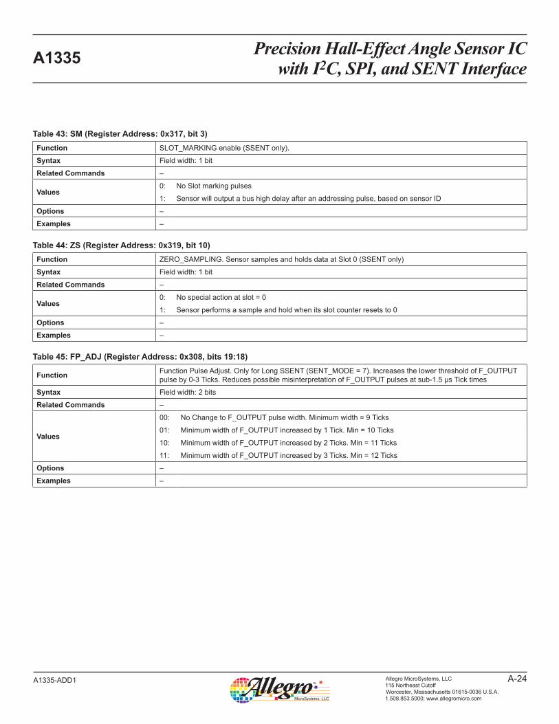
Precision Hall-Effect Angle Sensor ICwith I2C, SPI, and SENT InterfaceA1335
A-24Allegro MicroSystems, LLC115 Northeast CutoffWorcester, Massachusetts 01615-0036 U.S.A.1.508.853.5000; www.allegromicro.com
A1335-ADD1
Table 43: SM (Register Address: 0x317, bit 3)Function SLOT_MARKING enable (SSENT only).
Syntax Field width: 1 bit
Related Commands –
Values0: No Slot marking pulses
1: Sensor will output a bus high delay after an addressing pulse, based on sensor ID
Options –
Examples –
Table 44: ZS (Register Address: 0x319, bit 10)Function ZERO_SAMPLING. Sensor samples and holds data at Slot 0 (SSENT only)
Syntax Field width: 1 bit
Related Commands –
Values0: No special action at slot = 0
1: Sensor performs a sample and hold when its slot counter resets to 0
Options –
Examples –
Table 45: FP_ADJ (Register Address: 0x308, bits 19:18)
Function Function Pulse Adjust. Only for Long SSENT (SENT_MODE = 7). Increases the lower threshold of F_OUTPUT pulse by 0-3 Ticks. Reduces possible misinterpretation of F_OUTPUT pulses at sub-1.5 µs Tick times
Syntax Field width: 2 bits
Related Commands –
Values
00: No Change to F_OUTPUT pulse width. Minimum width = 9 Ticks
01: Minimum width of F_OUTPUT increased by 1 Tick. Min = 10 Ticks
10: Minimum width of F_OUTPUT increased by 2 Ticks. Min = 11 Ticks
11: Minimum width of F_OUTPUT increased by 3 Ticks. Min = 12 Ticks
Options –
Examples –

Precision Hall-Effect Angle Sensor ICwith I2C, SPI, and SENT InterfaceA1335
A-25Allegro MicroSystems, LLC115 Northeast CutoffWorcester, Massachusetts 01615-0036 U.S.A.1.508.853.5000; www.allegromicro.com
A1335-ADD1
I2C™ is a trademark of Philips Semiconductors.
Copyright ©2016, Allegro MicroSystems, LLCAllegro MicroSystems, LLC reserves the right to make, from time to time, such departures from the detail specifications as may be required to
permit improvements in the performance, reliability, or manufacturability of its products. Before placing an order, the user is cautioned to verify that the information being relied upon is current.
Allegro’s products are not to be used in any devices or systems, including but not limited to life support devices or systems, in which a failure of Allegro’s product can reasonably be expected to cause bodily harm.
The information included herein is believed to be accurate and reliable. However, Allegro MicroSystems, LLC assumes no responsibility for its use; nor for any infringement of patents or other rights of third parties which may result from its use.
Revision HistoryNumber Date Descriptioon
– July 15, 2016 Initial release