A Wideband 220 GHz, 50 W Serpentine Waveguide Amplifier · A Wideband 220 GHz, 50 W Serpentine...
5
Abstract—Final assembly is underway for a 220 GHz, 50 W serpentine waveguide vacuum electron amplifier showcasing a novel embedded monofilament microfabrication technique based on UV-LIGA. Three microfabricated circuits from the same wafer exhibited matching frequency response characteristics. Cold testing of the beryllia vacuum windows shows bandwidth in excess of 25 GHz. A demonstration of the tube is expected by the end of 2012. I. INTRODUCTION AND BACKGROUND LTRAVIOLET photolithography techniques along with copper electroforming (collectively, UV-LIGA) are being developed at the U.S. Naval Research Laboratory in order to span the spectrum from under 100 GHz through 1 THz [1-2]. With use of a Patent-Pending embedded polymer monofilament UV-LIGA technique [3], 3D all- copper structures have been demonstrated that allow arbitrarily small beam tunnels to be fabricated to arbitrary length along with slow-wave amplifier circuits. These techniques have been demonstrated at W-band (95 GHz), G- band (220 GHz), and 670 GHz to date. These frequencies provide jam-proof communication links and high resolution imaging by virtue of the inherently short wavelengths [4]. II. AMPLIFIER STATUS This serpentine waveguide (SWG) amplifier is designed to operate from a single, round 11.7 kV, 120 mA electron beam; other design parameters are listed in Table I. Figure 1 shows the final brazed body assembly of the tube along with the cold test setup. Figure 2 shows the predicted gain curve in MAGIC 3D producing 18 dB small signal gain with a 15.5 GHz bandwidth [5-6]. Windows made from BeO are predicted to yield a -30 dB reflection over a 20 GHz bandwidth. Using a CPI 5W EIK amplifier as a driver, over 60 W output power is expected from the tube. III. CIRCUIT FABRICATION To create reliable, high vertical aspect ratio serpentine features as required, a UV-LIGA technique was employed in two layers (Figure 3). The second layer made use of polymer monofilaments embedded in the SU-8 photoresist in order to hold the shape of the electron beam tunnels while the ultraviolet passed through a lithographic mask to create the serpentine patterns [7-8]. TABLE I: Amplifier Operating Parameters Beam voltage 11.7 kV Beam current 120 mA Beam tunnel diam 190 um Small Sig. Gain 18 dB Bandwidth 15.5 GHz Max Power Out 63 W Number of gaps 64 Figure 1. (Top) Final brazed body assembly. (Bottom) Pre- braze assembly under cold test from 140 GHz to 325 GHz. Colin D. Joye a , Alan M. Cook a , Jeffrey P. Calame a , David K. Abe a , Khanh T. Nguyen b , Edward L. Wright b , Takuji Kimura c , Baruch Levush a a Naval Research Laboratory, Code 6840, Washington, DC 20375 USA b Beam-Wave Research, Inc., Bethesda MD 20814 USA c Communications and Power Industries, Inc., Palo Alto CA 94304 USA A Wideband 220 GHz, 50 W Serpentine Waveguide Amplifier U 67
Transcript of A Wideband 220 GHz, 50 W Serpentine Waveguide Amplifier · A Wideband 220 GHz, 50 W Serpentine...

Abstract—Final assembly is underway for a 220 GHz, 50 W
serpentine waveguide vacuum electron amplifier showcasing a novel embedded monofilament microfabrication technique based on UV-LIGA. Three microfabricated circuits from the same wafer exhibited matching frequency response characteristics. Cold testing of the beryllia vacuum windows shows bandwidth in excess of 25 GHz. A demonstration of the tube is expected by the end of 2012.
I. INTRODUCTION AND BACKGROUND LTRAVIOLET photolithography techniques along with copper electroforming (collectively, UV-LIGA) are
being developed at the U.S. Naval Research Laboratory in order to span the spectrum from under 100 GHz through 1 THz [1-2]. With use of a Patent-Pending embedded polymer monofilament UV-LIGA technique [3], 3D all-copper structures have been demonstrated that allow arbitrarily small beam tunnels to be fabricated to arbitrary length along with slow-wave amplifier circuits. These techniques have been demonstrated at W-band (95 GHz), G-band (220 GHz), and 670 GHz to date. These frequencies provide jam-proof communication links and high resolution imaging by virtue of the inherently short wavelengths [4].
II. AMPLIFIER STATUS This serpentine waveguide (SWG) amplifier is designed
to operate from a single, round 11.7 kV, 120 mA electron beam; other design parameters are listed in Table I. Figure 1 shows the final brazed body assembly of the tube along with the cold test setup. Figure 2 shows the predicted gain curve in MAGIC 3D producing 18 dB small signal gain with a 15.5 GHz bandwidth [5-6]. Windows made from BeO are predicted to yield a -30 dB reflection over a 20 GHz bandwidth. Using a CPI 5W EIK amplifier as a driver, over 60 W output power is expected from the tube.
III. CIRCUIT FABRICATION To create reliable, high vertical aspect ratio serpentine
features as required, a UV-LIGA technique was employed in two layers (Figure 3). The second layer made use of polymer monofilaments embedded in the SU-8 photoresist in order to hold the shape of the electron beam tunnels while the ultraviolet passed through a lithographic mask to create the serpentine patterns [7-8].
TABLE I: Amplifier Operating Parameters
Beam voltage 11.7 kV Beam current 120 mA
Beam tunnel diam 190 um Small Sig. Gain 18 dB
Bandwidth 15.5 GHz Max Power Out 63 W Number of gaps 64
Figure 1. (Top) Final brazed body assembly. (Bottom) Pre-braze assembly under cold test from 140 GHz to 325 GHz.
Colin D. Joyea, Alan M. Cooka, Jeffrey P. Calamea, David K. Abea, Khanh T. Nguyenb, Edward L. Wrightb, Takuji Kimurac, Baruch Levusha
aNaval Research Laboratory, Code 6840, Washington, DC 20375 USA bBeam-Wave Research, Inc., Bethesda MD 20814 USA
cCommunications and Power Industries, Inc., Palo Alto CA 94304 USA
A Wideband 220 GHz, 50 W Serpentine Waveguide Amplifier
U
67

Report Documentation Page Form ApprovedOMB No. 0704-0188
Public reporting burden for the collection of information is estimated to average 1 hour per response, including the time for reviewing instructions, searching existing data sources, gathering andmaintaining the data needed, and completing and reviewing the collection of information. Send comments regarding this burden estimate or any other aspect of this collection of information,including suggestions for reducing this burden, to Washington Headquarters Services, Directorate for Information Operations and Reports, 1215 Jefferson Davis Highway, Suite 1204, ArlingtonVA 22202-4302. Respondents should be aware that notwithstanding any other provision of law, no person shall be subject to a penalty for failing to comply with a collection of information if itdoes not display a currently valid OMB control number.
1. REPORT DATE MAR 2013
2. REPORT TYPE N/A
3. DATES COVERED -
4. TITLE AND SUBTITLE A Wideband 220 GHz, 50 W Serpentine Waveguide Amplifier
5a. CONTRACT NUMBER
5b. GRANT NUMBER
5c. PROGRAM ELEMENT NUMBER
6. AUTHOR(S) 5d. PROJECT NUMBER
5e. TASK NUMBER
5f. WORK UNIT NUMBER
7. PERFORMING ORGANIZATION NAME(S) AND ADDRESS(ES) Naval Research Laboratory, Code 6840, Washington, DC 20375 USA
8. PERFORMING ORGANIZATIONREPORT NUMBER
9. SPONSORING/MONITORING AGENCY NAME(S) AND ADDRESS(ES) 10. SPONSOR/MONITOR’S ACRONYM(S)
11. SPONSOR/MONITOR’S REPORT NUMBER(S)
12. DISTRIBUTION/AVAILABILITY STATEMENT Approved for public release, distribution unlimited
13. SUPPLEMENTARY NOTES See also ADB387878. GOMACTech -13 Government Microcircuit Applications and Critical TechnologyConference (38th) on Microelectronics for Net-Enabled and Cyber Transformational Technologies. Held inLas Vegas, Nevada on 11-14 March 2013
14. ABSTRACT Final assembly is underway for a 220 GHz, 50 W serpentine waveguide vacuum electron amplifiershowcasing a novel embedded monofilament microfabrication technique based on UV-LIGA. Threemicrofabricated circuits from the same wafer exhibited matching frequency response characteristics. Coldtesting of the beryllia vacuum windows shows bandwidth in excess of 25 GHz. A demonstration of the tubeis expected by the end of 2012.
15. SUBJECT TERMS
16. SECURITY CLASSIFICATION OF: 17. LIMITATION OF ABSTRACT
SAR
18. NUMBEROF PAGES
4
19a. NAME OFRESPONSIBLE PERSON
a. REPORT unclassified
b. ABSTRACT unclassified
c. THIS PAGE unclassified
Standard Form 298 (Rev. 8-98) Prescribed by ANSI Std Z39-18

Figure 2. (Top) MAGIC 3D Prediction of amplifier performance (solid) and HFSS prediction of window performance (dashed). (Bottom) Drive curve prediction in MAGIC 3D showing over 60 W output power at 220 GHz.
After the SU-8 molds have been formed around the
polymer filament, the wafer is placed in an electroforming bath to deposit copper. The wafers are ground to thickness and polished, followed by a molten salt bath to remove the SU-8 [7]. After dicing to size and final lapping to thickness, the circuits are completed by brazing a flat cover piece on top. Figure 4 shows various features of a good circuit both before and after brazing.
IV. COLD TESTING The most important part of the microfabrication process is
cold testing the circuits and windows to ensure they were fabricated correctly. Using vector network analysis covering G- and H-bands (140-220 GHz and 220-325 GHz), the circuits are fully characterized, including pertinent stopbands near 300 GHz. During the cold testing, however, stopbands began appearing right in the operating band around 220 GHz. These stopbands can easily lead to oscillation since the electromagnetic waves cannot penetrate through the circuit. Figure 5 compares several circuits with varying degrees of stopbands at 220 GHz. It became apparent that slight misalignment of the beam tunnel in the planes of the serpentine variation breaks periodicity into a bi-periodic-like structure, which opens a new stopband at the point in the
Figure 3. Two-layer embedded polymer monofilament method. (a) The first layer of the circuit is produced by UV-LIGA with the photoresist left behind in the electroformed copper, which is ground and polished to the desired thickness, (b) the monofilament is fixed in place over the first layer, (c) the UV-LIGA process is performed again to create a second layer on top of the first with the monofilament buried inside, (d) dicing to size and the removal of the monofilament and photoresist completes the structure. Beam tunnel location shown by dotted line
Figure 4. (a) Photo of SWG circuit with beam tunnel prior to brazing a flat cover on. Shown with 0.0072 inch diameter gage pin inserted through beam tunnel. (b) Zoom in view of circuit with the gage pin shown inserted, (c) view of the ideal mask pattern, (d) view of input waveguide in completed circuit after brazing, (e) view of beam tunnel hole on brazed circuit showing a clean hole by green backlighting.
68
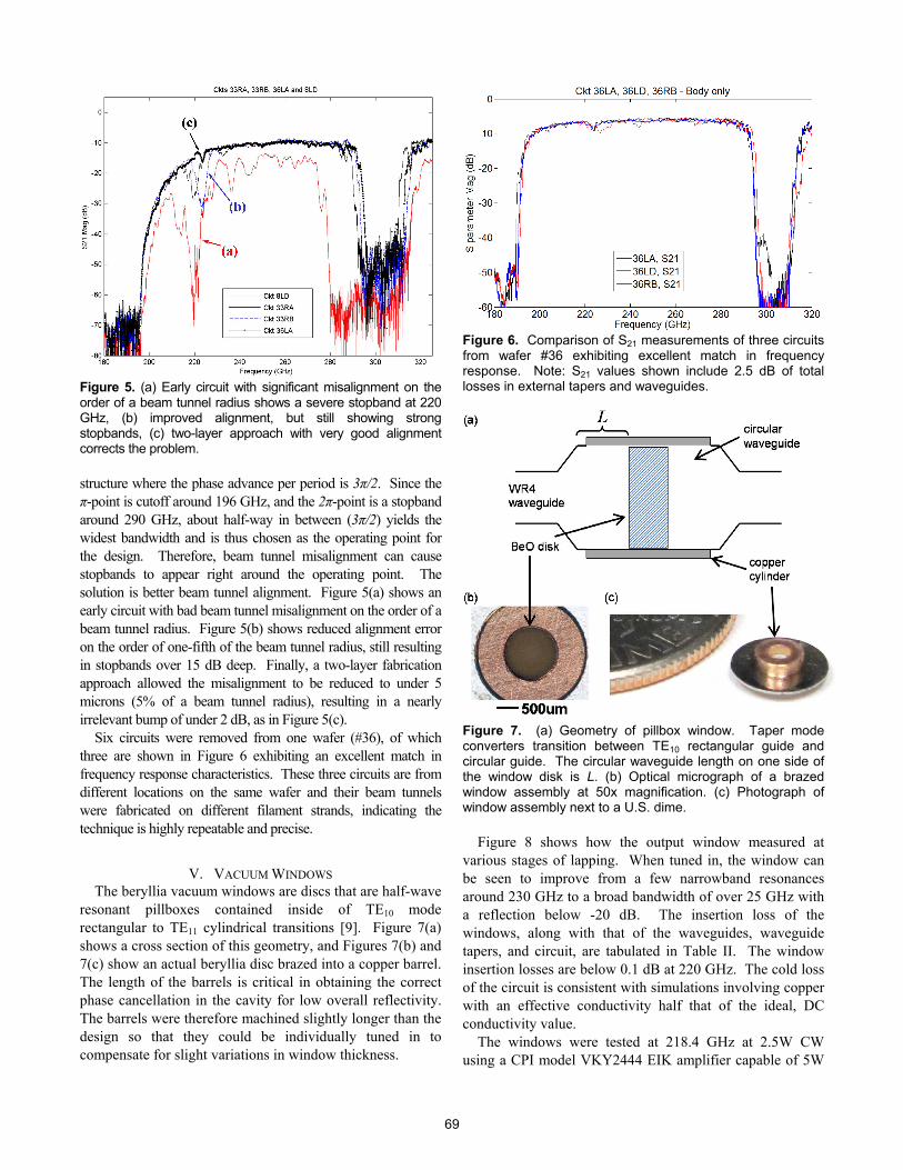
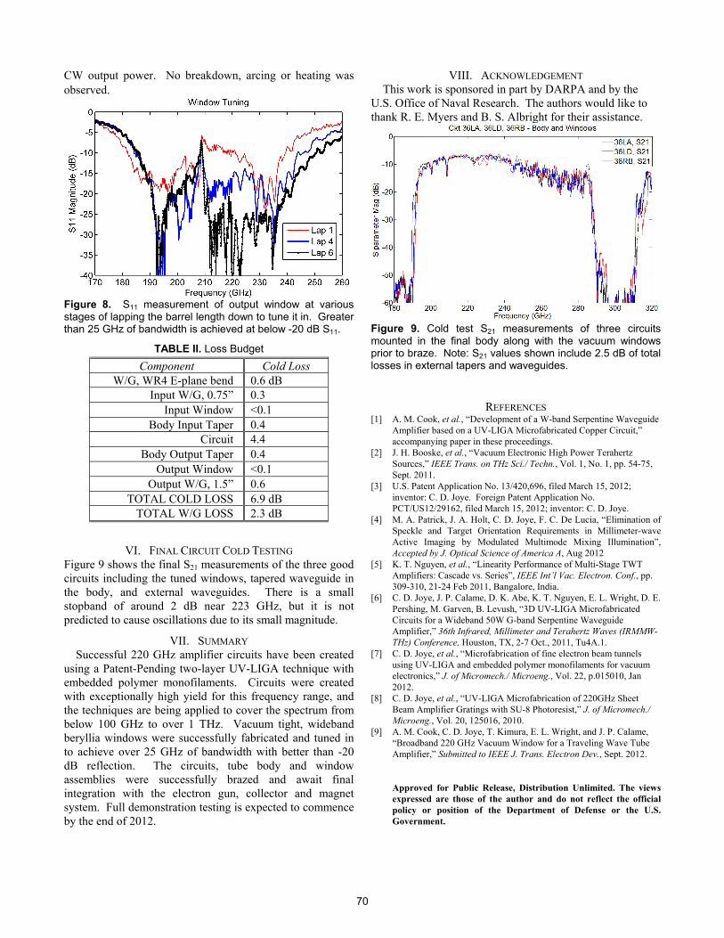
Figure 5. (a) Early circuit with significant misalignment on the order of a beam tunnel radius shows a severe stopband at 220 GHz, (b) improved alignment, but still showing strong stopbands, (c) two-layer approach with very good alignment corrects the problem. structure where the phase advance per period is 3π/2. Since the π-point is cutoff around 196 GHz, and the 2π-point is a stopband around 290 GHz, about half-way in between (3π/2) yields the widest bandwidth and is thus chosen as the operating point for the design. Therefore, beam tunnel misalignment can cause stopbands to appear right around the operating point. The solution is better beam tunnel alignment. Figure 5(a) shows an early circuit with bad beam tunnel misalignment on the order of a beam tunnel radius. Figure 5(b) shows reduced alignment error on the order of one-fifth of the beam tunnel radius, still resulting in stopbands over 15 dB deep. Finally, a two-layer fabrication approach allowed the misalignment to be reduced to under 5 microns (5% of a beam tunnel radius), resulting in a nearly irrelevant bump of under 2 dB, as in Figure 5(c). Six circuits were removed from one wafer (#36), of which three are shown in Figure 6 exhibiting an excellent match in frequency response characteristics. These three circuits are from different locations on the same wafer and their beam tunnels were fabricated on different filament strands, indicating the technique is highly repeatable and precise.
V. VACUUM WINDOWS The beryllia vacuum windows are discs that are half-wave
resonant pillboxes contained inside of TE10 mode rectangular to TE11 cylindrical transitions [9]. Figure 7(a) shows a cross section of this geometry, and Figures 7(b) and 7(c) show an actual beryllia disc brazed into a copper barrel. The length of the barrels is critical in obtaining the correct phase cancellation in the cavity for low overall reflectivity. The barrels were therefore machined slightly longer than the design so that they could be individually tuned in to compensate for slight variations in window thickness.
Figure 6. Comparison of S21 measurements of three circuits from wafer #36 exhibiting excellent match in frequency response. Note: S21 values shown include 2.5 dB of total losses in external tapers and waveguides.
Figure 7. (a) Geometry of pillbox window. Taper mode converters transition between TE10 rectangular guide and circular guide. The circular waveguide length on one side of the window disk is L. (b) Optical micrograph of a brazed window assembly at 50x magnification. (c) Photograph of window assembly next to a U.S. dime.
Figure 8 shows how the output window measured at various stages of lapping. When tuned in, the window can be seen to improve from a few narrowband resonances around 230 GHz to a broad bandwidth of over 25 GHz with a reflection below -20 dB. The insertion loss of the windows, along with that of the waveguides, waveguide tapers, and circuit, are tabulated in Table II. The window insertion losses are below 0.1 dB at 220 GHz. The cold loss of the circuit is consistent with simulations involving copper with an effective conductivity half that of the ideal, DC conductivity value.
The windows were tested at 218.4 GHz at 2.5W CW using a CPI model VKY2444 EIK amplifier capable of 5W
69
CW output power. No breakdown, arcing or heating was observed.
Figure 8. S11 measurement of output window at various stages of lapping the barrel length down to tune it in. Greater than 25 GHz of bandwidth is achieved at below -20 dB S11.
TABLE II. Loss Budget
Component Cold Loss W/G, WR4 E-plane bend 0.6 dB
Input W/G, 0.75” 0.3 Input Window <0.1
Body Input Taper 0.4 Circuit 4.4
Body Output Taper 0.4 Output Window <0.1
Output W/G, 1.5” 0.6 TOTAL COLD LOSS 6.9 dB
TOTAL W/G LOSS 2.3 dB
VI. FINAL CIRCUIT COLD TESTING Figure 9 shows the final S21 measurements of the three good circuits including the tuned windows, tapered waveguide in the body, and external waveguides. There is a small stopband of around 2 dB near 223 GHz, but it is not predicted to cause oscillations due to its small magnitude.
VII. SUMMARY Successful 220 GHz amplifier circuits have been created
using a Patent-Pending two-layer UV-LIGA technique with embedded polymer monofilaments. Circuits were created with exceptionally high yield for this frequency range, and the techniques are being applied to cover the spectrum from below 100 GHz to over 1 THz. Vacuum tight, wideband beryllia windows were successfully fabricated and tuned in to achieve over 25 GHz of bandwidth with better than -20 dB reflection. The circuits, tube body and window assemblies were successfully brazed and await final integration with the electron gun, collector and magnet system. Full demonstration testing is expected to commence by the end of 2012.
VIII. ACKNOWLEDGEMENT This work is sponsored in part by DARPA and by the
U.S. Office of Naval Research. The authors would like to thank R. E. Myers and B. S. Albright for their assistance.
Figure 9. Cold test S21 measurements of three circuits mounted in the final body along with the vacuum windows prior to braze. Note: S21 values shown include 2.5 dB of total losses in external tapers and waveguides.
REFERENCES [1] A. M. Cook, et al., “Development of a W-band Serpentine Waveguide
Amplifier based on a UV-LIGA Microfabricated Copper Circuit,” accompanying paper in these proceedings.
[2] J. H. Booske, et al., “Vacuum Electronic High Power Terahertz Sources,” IEEE Trans. on THz Sci./ Techn., Vol. 1, No. 1, pp. 54-75, Sept. 2011.
[3] U.S. Patent Application No. 13/420,696, filed March 15, 2012; inventor: C. D. Joye. Foreign Patent Application No. PCT/US12/29162, filed March 15, 2012; inventor: C. D. Joye.
[4] M. A. Patrick, J. A. Holt, C. D. Joye, F. C. De Lucia, “Elimination of Speckle and Target Orientation Requirements in Millimeter-wave Active Imaging by Modulated Multimode Mixing Illumination”, Accepted by J. Optical Science of America A, Aug 2012
[5] K. T. Nguyen, et al., “Linearity Performance of Multi-Stage TWT Amplifiers: Cascade vs. Series”, IEEE Int’l Vac. Electron. Conf., pp. 309-310, 21-24 Feb 2011, Bangalore, India.
[6] C. D. Joye, J. P. Calame, D. K. Abe, K. T. Nguyen, E. L. Wright, D. E. Pershing, M. Garven, B. Levush, “3D UV-LIGA Microfabricated Circuits for a Wideband 50W G-band Serpentine Waveguide Amplifier,” 36th Infrared, Millimeter and Terahertz Waves (IRMMW-THz) Conference, Houston, TX, 2-7 Oct., 2011, Tu4A.1.
[7] C. D. Joye, et al., “Microfabrication of fine electron beam tunnels using UV-LIGA and embedded polymer monofilaments for vacuum electronics,” J. of Micromech./ Microeng., Vol. 22, p.015010, Jan 2012.
[8] C. D. Joye, et al., “UV-LIGA Microfabrication of 220GHz Sheet Beam Amplifier Gratings with SU-8 Photoresist,” J. of Micromech./ Microeng., Vol. 20, 125016, 2010.
[9] A. M. Cook, C. D. Joye, T. Kimura, E. L. Wright, and J. P. Calame, “Broadband 220 GHz Vacuum Window for a Traveling Wave Tube Amplifier,” Submitted to IEEE J. Trans. Electron Dev., Sept. 2012. Approved for Public Release, Distribution Unlimited. The views expressed are those of the author and do not reflect the official policy or position of the Department of Defense or the U.S. Government.
70


![DESIGN OF A WIDEBAND VIVALDI ANTENNA ARRAY … · DESIGN OF A WIDEBAND VIVALDI ANTENNA ARRAY ... Two double-ridged waveguide TEM horn antennas ... Double transition in HFSS[R] ...](https://static.fdocuments.us/doc/165x107/5ae77def7f8b9a3d3b8e9763/design-of-a-wideband-vivaldi-antenna-array-of-a-wideband-vivaldi-antenna-array.jpg)