A U NBS TECHNICAL NOTE COl PUl - NASA · iME1 OF NBS TECHNICAL NOTE 702 BUCATION 4~e t r-- ... The...
50
A U DEPI COl PUl / tio@~41 A 3 4 iME1 OF NBS TECHNICAL NOTE 702 BUCATION 4~e t r-- 'Bu'reau (ACCESSIONs,o, U.S. PARTMENT OF COMMERCE Bureau } (ACCESSION NUMBER) mI of E MPAS Rsr REET GL/1 Standards o, 47 2-133( unclas 11107 (PAGI~% ~36)IjETI ROCESS (IA SEA iCO DUCTOS ATERIALS F68 SEMI1COINOCO QatryR0r'r CONTROL, AND DEVICES Quarterly Report, 1 w.fl. Bullis (NactiOalCSCLura Aprt. -~ J D 1971 45 p of standards) Dec 1971 )E C I G3/14 https://ntrs.nasa.gov/search.jsp?R=19720005719 2018-08-18T19:17:52+00:00Z
Transcript of A U NBS TECHNICAL NOTE COl PUl - NASA · iME1 OF NBS TECHNICAL NOTE 702 BUCATION 4~e t r-- ... The...

A UDEPICOlPUl
/
tio@~41 A 3 4
iME1 OF NBS TECHNICAL NOTE 702BUCATION
4~e t
r--
'Bu'reau (ACCESSIONs,o,
U.S.PARTMENT
OFCOMMERCE
Bureau } (ACCESSION NUMBER) mI
of E MPAS Rsr REET GL/1Standards o,
47 2-133(
unclas11107
(PAGI~% ~36)IjETI ROCESS
(IA SEA iCO DUCTOS ATERIALS F68 SEMI1COINOCO QatryR0r'r
CONTROL, AND DEVICES Quarterly Report,
1
w.fl. Bullis (NactiOalCSCLuraAprt. -~ J D 1971 45 p
of standards) Dec 1971
)E
C
I
G3/14
https://ntrs.nasa.gov/search.jsp?R=19720005719 2018-08-18T19:17:52+00:00Z

NATIONAL BUREAU OF STANDARDS
The National Bureau of Standards' was established by an act of Congress March 3,1901. The Bureau's overall goal is to strengthen and advance the Nation's science andtechnology and facilitate their effective application for public benefit. To this end, theBureau conducts research and provides: (1) a basis for the Nation's physical measure-ment system, (2) scientific and technological services for industry and government, (3)a technical basis for equity in trade, and (4) technical services to promote public safety.The Bureau consists of the Institute for Basic Standards, the Institute for MaterialsResearch, the Institute for Applied Technology, the Center for Computer Sciences andTechnology, and the Office for Information Programs.
THE INSTITUTE FOR BASIC STANDARDS provides the central basis within theUnited States of a complete and consistent system of physical measurement; coordinatesthat system with measurement systems of other nations; and furnishes essential servicesleading to accurate and uniform physical measurements throughout the Nation's scien-tific community, industry, and commerce. The Institute consists of a Center for Radia-tion Research, an Office of Measurement Services and the following divisions:
Applied Mathematics-Electricity-Heat-Mechanics--Optical Physics-LinacRadiation2 -Nuclear Radiation-2-Applied Radiation2-Quantum Electronics3 -Electromagnetics3 -Time and Frequency3 -Laboratory Astrophysics3 --Cryo-genics3 .
THE INSTITUTE FOR MATERIALS RESEARCH conducts materials research lead-ing to improved methods of measurement, standards, and data on the properties ofwell-characterized materials needed by industry, commerce, educational institutions, andGovernment; provides advisory and research services to other Government agencies;and develops, produces, and distributes standard reference materials. The Institute con-sists of the Office of Standard Reference Materials and the following divisions:
Analytical Chemistry-Polymers-Metallurgy-Inorganic Materials-ReactorRadiation-Physical Chemistry.
THE INSTITUTE FOR APPLIED TECHNOLOGY provides technical services to pro-mote the use of available technology and to facilitate technological innovation in indus-try and Government; cooperates with public and private organizations leading to thedevelopment of technological standards (including mandatory safety standards), codesand methods of test; and provides technical advice and services to Government agenciesupon request. The Institute also monitors NBS engineering standards activities andprovides liaison between NBS and national and international engineering standardsbodies. The Institute consists of the following technical divisions and offices:
Engineering Standards Services-Weights and Measures-Flammable Fabrics-Invention and Innovation-Vehicle Systems Research-Product EvaluationTechnology-Building Research-Electronic Technology-Technical Analysis-Measurement Engineering.
THE CENTER FOR COMPUTER SCIENCES AND TECHNOLOGY conducts re-search and provides technical services designed to aid Government agencies in improv-ing cost effectiveness in the conduct of their programs through the selection, acquisition,and effective utilization of automatic data processing equipment; and serves as the prin-cipal focus within the executive branch for the development of Federal standards forautomatic data processing equipment, techniques, and computer languages. The Centerconsists of the following offices and divisions:
Information Processing Standards-Computer Information-Computer Services-Systems Development-Information Processing Technology.
THE OFFICE FOR INFORMATION PROGRAMS promotes optimum disseminationand accessibility of scientific information generated within NBS and other agencies ofthe Federal Government; promotes the development of the National Standard ReferenceData System and a system of information analysis centers dealing with the broaderaspects of the National Measurement System; provides appropriate services to ensurethat the NBS staff has optimum accessibility to the scientific information of the world,and directs the public information activities of the Bureau. The Office consists of thefollowing organizational units:
Office of Standard Reference Data-Office of Technical Information andPublications-Library-Office of Public Information-Office of InternationalRelations.
Headquarters and Laboratories at Gaithersburg, Maryland, unless otherwise noted; mailing address Washing.ton, D.C. 20234.
2 Part of the Center for Radiation Research.a Located at Boulder, Colorado 80302.

UNITED STATES DEPARTMENT OF COMMERCEMaurice H. Stans, Secretary
NATIONAL BUREAU OF STANDARDS * Lewis M. Branscomb, Director
TECHNICAL NOTE 702ISSUED DECEMBER 1971
Nat. Bur. Stand. (U.S.), Tech. Note 702, 45 pages (December 1971)CODEN: NBTNA
Methods of Measurement for SemiconductorMaterials, Process Control, and Devices
Quarterly Report
April 1 to June 30, 1971
Edited by W. Murray Bullis
Electronic Technology DivisionInstitute for Applied Technology
National Bureau of StandardsWashington, D.C. 20234
Jointly Supported by the National Bureau of Standards,the Defense Atomic Support Agency, the U.S. Navy
Strategic Systems Project Office, the U.S. Navy Electronic SystemsCommand, the Air Force Weapons Laboratory, the Air Force Cambridge Research
Laboratories, the Advanced Research Projects Agency, the Atomic Energy Commission,and the National Aeronautics and Space Administration
/iEAU oi
NBS Technical Notes are designed to supplement theBureau's regular publications program. They provide ameans for making available scientific data that are oftransient or limited interest. Technical Notes may belisted or referred to in the open literature.
For sale by the Superintendent of Documents, U.S. Government Printing Office,Washington, D.C., 20402.(Order by SD Catalog No. C 13.46:702). Price 50 cents.
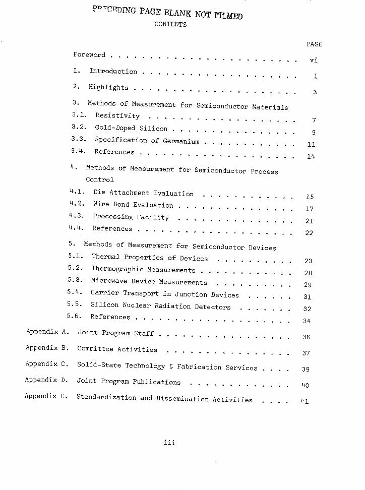
PP'CMDING PAGE BLANK NOT FILMEDCONTENTS
PAGE
Foreword ........................ vi
1. Introduction ................... 1. 1
2. Highlights ................... .. 3
3. Methods of Measurement for Semiconductor Materials
3.1. Resistivity . . . . . . . . . . . . . . . . . . . 7
3.2. Gold-Doped Silicon . . . . . . . . . . . . . . . . 9
3.3. Specification of Germanium . . . . . . . . .... 11
3.4. References . . . . . . . . . . . . . . . . . 14
4. Methods of Measurement for Semiconductor Process
Control
4.1. Die Attachment Evaluation . . . . . . . . .... 15
4.2. Wire Bond Evaluation . . . . . . . . . . . .... 17
4.3. Processing Facility . . . . . . . . . . . .... 21
4.4. References . . . . . . . . . . . . . . . . . . 22
5. Methods of Measurement for Semiconductor Devices
5.1. Thermal Properties of Devices . . . . . . .... 23
5.2. Thermographic Measurements . . . . . . . . .... 28
5.3. Microwave Device Measurements . . . . . . .... 29
5.4. Carrier Transport in Junction Devices . . . . .. 31
5.5. Silicon Nuclear Radiation Detectors ....... 32
5.6. References .. . . . . . . . . . . . . . . . . . 34
Appendix A. Joint Program Staff ................. 36
Appendix B. Committee Activities ................ 37
Appendix C. Solid-State Technology & Fabrication Services . . .. 39
Appendix D. Joint Program Publications . . . . . . . . . .... 40
Appendix E. Standardization and Dissemination Activities . ... . 41
iii

LIST OF FIGURES
PAGE
1. Resistivity as a function of gold concentration in p-typesilicon .. . . . . . . . . . . . . . . . . . . ..... 10
2. Infrared response spectra of three germanium gamma-raydetectors . . . . . . . . . . . . . . . . . . ....... 13
3. Thermal response curves for diodes with 20-percent voidareas and their controls. . . . . . . . . . . . . ...... 16
4. Thermal response curves for diodes with 40-percent voidareas and their controls. . . . . . . . . . . . . ...... 16
5. SEM photomicrograph of typical ribbon-wire first bond . . . . 18
6. SEM photomicrograph of typical ribbon-wire second bond. . . . 18
7. SEM photomicrograph of overbonded ribbon-wire first bond. . . 18
8. SEM photomicrograph of lift-off pattern of ribbon-wirefirst bond. . . . . . . . . . . . . . . .. ...... 18
9. SEM photomicrograph of lift-off pattern of ribbon-wiresecond bond. . . . . . . . . . . . . . . ...... 18
10. Circuits for measuring thermal resistance of transistors. . . 24
11. Base current (solid curves) and base-emitter voltage (dashed)curves) as a function of power for a silicon power transistorshowing onset of hot spots. . . . . . . . . . . . ...... 26
12. Circuits for measuring common-emitter current gain oftransistors . . . . . . . . . . . . . . . . . . ...... 26
iv

LIST OF TABLES
PAGE
1. Results of Repetitive Junction-to-Case TemperatureDifference Measurements after Equipment Improvements ...... 16
2. Comparison of Thermal Resistance Measured usingCommon-Emitter and Common-Base Circuits . . . . . . . . . ... 26
v
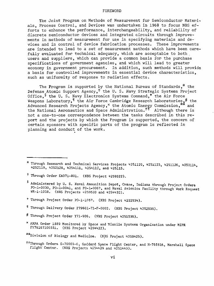
FOREWORD
The Joint Program on Methods of Measurement for Semiconductor Materi-als, Process Control, and Devices was undertaken in 1968 to focus NBS ef-forts to enhance the performance, interchangeability, and reliability ofdiscrete semiconductor devices and integrated circuits through improve-ments in methods of measurement for use in specifying materials and de-vices and in control of device fabrication processes. These improvementsare intended to lead to a set of measurement methods which have been care-fully evaluated for technical adequacy, which are acceptable to bothusers and suppliers, which can provide a common basis for the purchasespecifications of government agencies, and which will lead to greatereconomy in government procurement. In addition, such methods will providea basis for controlled improvements in essential device characteristics,such as uniformity of response to radiation effects.
The Program is supported by the National Bureau of Standards,* theDefense Atomic Support Agency,t the U. S. Navy Strategic Systems ProjectOffice,5 the U. S. Navy Electronics Systems Command,+ the Air ForceWeapons Laboratory,7 the Air Force Cambridge Research Laboratories # theAdvanced Research Projects Agency,x the Atomic Energy Commission,*' andthe National Aeronautics and Space Administration.t Although there isnot a one-to-one correspondence between the tasks described in this re-port and the projects by which the Program is supported, the concern ofcertain sponsors with specific parts of the program is reflected inplanning and conduct of the work.
Through Research and Technical Services Projects 4251120, 4251123, 4251126, 4252114,4252119, 4252128, 4254111, 4254112, and 425115.
t Through Order EAO71-801. (NBS Project 4259522).
§ Administered by U. S. Naval Ammunition Depot, Crane, Indiana through Project OrdersPO-1-0030, PO-1-0041, and PO-1-0067, and Naval Avionics Facility through Work RequestWR-1-1038. (NBS Projects 4259533 and 4254432).
+ Through Project Order PO-1-1057. (NBS Project 4252534).
¶ Through Delivery Order F29601-71-F-0002. (NBS Project 4252535).
# Through Project Order Y71-906. (NBS Project 4251536).
X ARPA Order 1889 Monitored by Space and Missile Systems Organization under MIPRFY76167100331. (NBS Project 4254422).
**Division of Biology and Medicine. (NBS Project 4259425).
t"Through Orders S-70003-G, Goddard Space Flight Center, and H-76553A, Marshall SpaceFlight Center. (NBS Projects 4254429 and 4251449).
vi

METHODS OF MEASUREMENT FORSEMICONDUCTOR MATERIALS, PROCESS CONTROL, AND DEVICES
Quarterly ReportApril 1 to June 30, 1971
This quarterly progress report, twelfth of a series, de-scribes NBS activities directed toward the development ofmethods of measurement for semiconductor materials, processcontrol, and devices. Significant accomplishments during thisreporting period include a demonstration of the high sensitiv-ity of the infrared response technique by the identificationof gold in a germanium diode doped to a level of 1011 goldatoms per cubic centimeter, verification that transient thermalresponse is significantly more sensitive to the presence ofvoids in die attachment than steady-state thermal resistance,and development of a simplified circuit for screening transis-tors for susceptibility to hot-spot formation by the current-gain technique. Work is continuing on measurement of resis-tivity of semiconductor crystals; study of gold-doped silicon;specification of germanium for gamma-ray detectors; evaluationof wire bonds and die attachment; measurement of thermal prop-erties of semiconductor devices, transit time and related car-rier transport properties injunction devices, and electricalproperties of microwave devices; and characterization of sili-con nuclear radiation detectors. Supplementary data concerningstaff, standards committee activities, technical services, andpublications are included as appendixes.
Key Words: Alpha-particle detectors; aluminum wire; basetransit time; carrier lifetime; die attachment; electricalproperties; epitaxial silicon; gamma-ray detectors; ger-manium; gold-doped silicon; methods of measurement; micro-electronics; microwave devices; nuclear radiation detectors;probe techniques (a-c); resistivity; semiconductor devices;semiconductor materials; semiconductor process control;silicon; thermal resistance; thermographic measurements;ultrasonic bonder; wire bonds.
1. INTRODUCTION
This is the twelfth quarterly report to the sponsors of the JointProgram on Methods of Measurement for Semiconductor Materials, ProcessControl, and Devices. It summarizes work on a wide variety of measure-ment methods that are being studied at the National Bureau of Standards.Since the Program is a continuing one, the results and conclusions report-ed here are subject to modification and refinement.
1
INTRODUCTION
The work of the Program is divided into a number of tasks, each di-
rected toward the study of a particular material or device property or
measurement technique. This report is subdivided according to thesetasks, Highlights of activity during the quarter are given in Section 2.Section 3 deals with tasks on methods of measurement for materials;Section 4, with those on methods of measurement for process control; and
Section 5, with those on methods of measurement for devices. Referencesfor each section are listed in a separate subsection at the end of thatsection.
The report of each task includes the long-term objective, a narra-
tive description of progress made during this reporting period, and alisting of plans for the immediate future. Additional information con-cerning the material reported may be obtained directly from individualstaff members connected with the task as indicated throughout the report.The organization of the Joint Program staff and telephone numbers arelisted in Appendix A.
An important part of the work that frequently goes beyond the taskstructure is participation in the activities of various technical stand-ardizing committees. The list of personnel involved with this work given
in Appendix B suggests the extent of this participation. Additional de-
tails of current efforts in this area are given in Section 2.
Background material on the Program and individual tasks may be foundin earlier reports in this series as listed in Appdndix D. From time totime, publications-that describe some aspect of the program in greaterdetail are prepared. Current publications are also listed in Appendix D.
2

2. HIGHLIGHTS
Significant accomplishments during this reporting period include ademonstration of the high sensitivity of the infrared response techniqueby the identification of gold in a germanium diode doped with 1011 goldatoms per cubic centimeter, verification that transient thermal responseis significantly more sensitive to the presence of voids in die attach-ment than steady-state thermal resistance, and development of a simpli-fied circuit for screening transistors for susceptibility to hot-spotformation by the current-gain technique. Highlights of these and othertechnical activities are presented in this section; details are given insubsequent sections of the report. This section concludes with a summaryof standardization activities being carried out by program staff members.
Resistivity - Principal emphasis was placed on completion of measure-ments on wafers with chem-mechanically polished surfaces in the study ofthe effect of current level and probe force on resistivity as measured bythe four-probe method and on coordination and analysis of round-robininterlaboratory tests being conducted in cooperation with ASTM CommitteeF-1 on Electronics. In other work evidence was found that suggests thatthe difficulty encountered in fabrication of diodes that are satisfactoryfor capacitance-voltage measurements is due to crystal defects that mightbe introduced during wafer preparation or during subsequent processingsteps. Work in support of spreading resistance methods continued withfurther efforts to obtain high-quality scanning electron microscope photo-micrographs of probe damage to silicon.
GoZd-Doped SiZicon - Work continued in preparing and evaluating gold-doped silicon wafers in the extensive series of measurements of resisti-vity, Hall coefficient, and gold concentration outlined previously.Results of the study of lateral uniformity of diffused gold as determinedby x-ray fluorescence with the scanning electron microscope suggesteither that the clusters which form do not extend as much as 5 pm belowthe surface or that the gold concentration in a cluster decreases rapidlywith distance below the surface. Preliminary measurements of carrier dif-fusion length by the surface photovoltage technique were attempted ongold-diffused Hall bars.
Specification of Germanium - Study of methods for measuring lithium-ion drift mobility in germanium has been completed with the adoption byASTM Committee F-1 of a method based on technology developed under thistask. Work on methods for measuring carrier trapping in germanium iscontinuing in cooperation with the committee. The improved infrared re-sponse technique was used to study eight germanium diodes; gold was iden-tified in one doped with 1011 gold atoms per cubic centimeter. Applica-tion of the infrared response method to silicon devices continued.
Die Attachment Evaluation - Modification of the die attachment eval-uation equipment to increase its power handling capabilities and to in-crease the resolution of the digital voltmeter resulted in improved repro-ducibility of the measurements. Transient thermal response measurements
3

HIGHLIGHTS
for a heating-power pulse width of about 10 ms were shown to be more sen-sitive to the presence of 10-, 20-, and 40-percent void areas in diodedie attachment than steady-state thermal resistance measurements. Forthe particular device tested, a 10-percent void area appears to be thesmallest that can be detected by the thermal response technique; it isnot detectable by the thermal resistance technique.
Wire Bond EvaZuation - Work progressed on ribbon-wire bonding de-spite several continuing problems with both the bonding machine and thedimensional uniformity of the wire. Scanning electron microscope photo-micrographs were made of bonds and of lift-off patterns. Evaluation ofthe pull test on round-wire bonds was deferred due to serious mechanicalproblems with the round-wire bonding machine. A simple technique forrefinishing used bonding tools was devised. Assistance in the organiza-tion of a section on microelectronic bonding was provided in conjunctionwith the summer meeting of ASTM Committee F-1 at NBS. More than 40 rep-resentatives of device manufacturers, materials and equipment producers,and consumers attended. Ten areas in bonding were selected and taskforces were set up to take the necessary action.
Processing FaciZity - Principal effort is being expended on develop-ment of a process for fabricating diffused silicon diodes required in theresistivity task for the purpose of measuring resistivity as a functionof depth in bulk and epitaxial silicon wafers by the capacitance-voltagemethod.
Thermal Properties of Devices - Prototype circuits to measure tran-sistor thermal resistance and common-emitter current gain in the common-base operating mode were designed and built. These circuits are muchsimpler than the common-emitter circuits used up to this point becauseit is not necessary to use special circuitry in the base lead to controlthe collector current. In the case of the current-gain measurement, thesimplicity of the common-base circuit makes feasible a production-oriented current-gain screening technique for hot-spot formation. In acomparison of the effectiveness of the use of base-emitter junction volt-age as a screen for thermal instabilities with that of the common-emittercurrent gain it was found that while both were sensitive to constrictedhot-spots that exhibit thermal hysteresis the former was much less sen-sitive to the more amorphous, less constricted hot-spots that occur underhigher current, lower voltage operating conditions. A study was under-taken to determine the pulse conditions under which a power transistorcould be put into a constricted operating mode with thermal hysteresis.With repetitively pulsed collector excursions, it was found that hys-teresis occurred when the product of the magnitude of the voltage pulseand the duty cycle was equal to the steady-state voltage change requiredto initiate hysteresis from a given collector voltage below the d-c hot-spot initiation voltage. For singly pulsed excursions from variouscollector voltages below the d-c hot-spot initiation voltage, it wasfound that, for a given pulse width, the combined d-c and pulsed voltage
4

HIGHLIGHTS
required to initiate hot-spots increased as the starting d-c collectorvoltage level was reduced.
Microwave Device Measurements - To improve the precision of the lowintermediate-frequency conversion-loss measurements, an incremental mod-ulation technique has been introduced. With this technique, precisionis limited principally by the resolution of the attenuator used to setthe increment and by the mechanical stability of the waveguide systemrather than by the output resolution.
Carrier Transport in Junction Devices - The vector-voltmeter measure-ment system for measuring transistor delay time was assembled and prelim-inary tests were carried out. Two systems for the measurement of tran-sistor S-parameters in the 200 to 800 MHz range are being assembled. Ananalysis of the equivalent circuits of a transistor in the Sandia-typebridge and in the vector-voltmeter circuit has been made to relate themeasured delay time to various time constants and delay times within thedevice.
SiZicon NucZlear Radiation Detectors - Study of radiation damage ef-fects of 600-keV electrons and fast neutrons in lithium-drifted silicondetectors has been completed. A preliminary study of the effect of ex-posure of a silicon surface-barrier detector to dry ammonia and methanolvapor at various pressures was completed. No significant changes innoise level were observed during these tests.
Standardization Activities - Many of the standardization activitiesundertaken by program staff are broader than the technical tasks describ-ed in the following sections. These activities involve general staffsupport in committees, coordination of efforts which may encompass a va-riety of tasks, and participation in areas where no direct in-house tech-nical effort is underway. Standardization activities directly relatedto particular task areas are reported with the appropriate tasks. A sum-mary of standardization and dissemination activities during FY 1971 isgiven in Appendix E.
Twelve program staff members attended the regular summer meeting ofASTM Committee F-1 held at the NBS facilities in Gaithersburg. Programstaff members were instrumental in the organization of a new section onBonding of Subcommittee 7 on Hybrid Microelectronics (see Section 4.2).Mrs. K. 0. Leedy was appointed chairman of the section. J. R. Ehrsteinwas appointed chairman of the Resistivity Section of Subcommittee 6 onElectrical Measurements. W. M. Bullis was appointed member-at-large tothe Advisory Committee.
Activity in connection with JEDEC committees of the Electronic Indus-tries Association continued in a variety of areas. Contact with thechairman of Committee JC-21 on UHF and Microwave Diodes was renewed inorder to discuss the status of the microwave diode task and its relation
5
HIGHLIGHTS
to current industry requirements. F. F. Oettinger attended meetings ofCommittees JC-22 on Rectifier Diodes and Thyristors and JC-ll on Mechani-cal Standardization.
W. M. Bullis was appointed to the Planning Subcommittee of SAE Com-mittee H on Electronic Materials and Processes. F. F. Oettinger was ap-pointed to the Technical Program Committee for the March 1972 IEEE Inter-national Convention.
6
3. METHODS OF MEASUREMENT FOR SEMICONDUCTOR MATERIALS
3.1. RESISTIVITY
Objective: To develop methods suitable for use throughout the elec-tronics industry for measuring resistivity of bulk, epitaxial, and dif-fused silicon wafers.
Progress: Principal emphasis was placed on completion of measure-ments on wafers with chem-mechanically polished surfaces in the study ofthe effect of current level and probe force on resistivity as measured bythe four-probe method, and on coordination and analysis of round-robinsbeing conducted in cooperation with ASTM Committee F-1 on Electronics.In other work, evidence was found that suggests that the difficulty en-countered in fabrication of diodes that are satisfactory for capacitance-voltage measurements is due to crystal defects that might be introducedduring wafer preparation or during subsequent processing steps. Work insupport of spreading resistance methods continued with further efforts toobtain high-quality scanning electron microscope photomicrographs ofprobe damage to silicon. Study of probe impact momentum was deferred.
Four-Probe Method - Measurements were completed on seven silicon wa-fers with chem-mechanically polished surfaces in the study to determinethe effect of current level and probe force on the measurement of resis-tivity by the four-probe method. The procedure used was identical tothat used previously on mechanically polished slices (NBS Tech. Note 598,p. 7). Preliminary examination of the results suggests that the form ofthe current and probe-force dependence is virtually unchanged between themechanically polished and chem-mechanically polished surfaces on the samewafer. However, at any specific combination of current and probe forcethe resistivity measured on the chem-mechanically polished surface islower by 0.5 to 1.5 percent than that on the same wafer with a mechanical-ly polished surface. (J. R. Ehrstein and D. R. Ricks)
An auxiliary study has been started to try to relate variation in
measured resistivity with surface condition to amount of subsurface dam-age. Measurements of carrier diffusion length by the surface photovoltagemethod have been found to be sensitive to the nature of the specimen sur-face. Surface photovoltage measurements are being made on specimens withlapped, mechanically polished, and chem-mechanically polished surfaces todetermine qualitatively the extent of subsurface damage.
(J. R. Ehrstein, W. R. Thurber, W. E. Phillips, and A. W, Stallings)
Standardization Activities - A summary of the results of the round-robin on four-probe measurement of resistivity of silicon wafers in the5,000 to 20,000 .-cm range was presented to the Resistivity Section of
Committee F-1 at its June meeting. Seven laboratories participated inthe round-robin. Five silicon specimens and two analog resistance boxes[1] were circulated. Two p-type and one n-type specimen had room-temperature (230 C) resistivity around 6,000 -'cm; one n-type and one
7
RESISTIVITY
p-type specimen were supplied as 14,000 to 15,000 Q*cm. The analog boxesused for calibration had standard resistors of 1,000 and 10,000 Q.
No serious difficulties were encountered in measurement of the analogboxes; with resistors 300 times as large as the standard resistor in boththe current and potential leads, the maximum error in measuring the resis-tance of the standards was ±1.5 percent. Measurement of the 6,000-Q-cmn-type specimen resulted in a sample standard deviation of 3 to 4 percent,well within the precision quoted for wafers with resistivity between 500and 2,000 Q-cm [1]. Measurement of the 6,000-Q-cm p-type specimens andof both the higher resistivity specimens resulted in sample standard de-viations greater than 10 percent, considerably outside the precisionquoted for lower resistivity specimens [1].
Preliminary results of the round-robin on four-probe measurement ofresistivity of silicon epitaxial layers deposited on substrates of oppo-site conductivity type were also presented at the June meeting of Commit-tee F-1. Seven of the eleven scheduled participants had completed theirmeasurements. The results are being reviewed to determine whether theyare sufficient to support a precision statement in the standard methodnow under development for this test.
Capacitance-Voltage Method - Arrays of 20- and 30-mil (0.5- and0.75-mm) diameter diodes were fabricated in four 15-.-cm, n-type siliconslices by means of the same fabrication procedure previously used on1 Q-cm slices (see Section 4.3). Measurements of capacitance as a func-tion of voltage (C-V) were inhibited by insufficiently large breakdownvoltages on most of the diodes on the four wafers. Microscopic inspec-tion of these wafers revealed a pattern of linear defects present on mostof the devices on all four wafers. On each wafer all the linear defectswere oriented in the same direction over the entire wafer surface. Itwas also found that those few diodes which had acceptable breakdown volt-ages were characterized by an absence of these defects. All diodes thatcould be measured were located near the edge of the wafer where the four-probe resistivity values were not reliable so that valid comparison be-tween C-V and four-probe data was impossible. At present the varioussteps in the processing procedure are being scrutinized to try to deter-mine the origin of these defects so that the procedure can be modifiedto produce a greater yield of diodes with acceptable breakdown voltages.
Preliminary measurements were made on 20-mil (0.5-mm) diameter,0.5 pm deep, boron-diffused, mesa diodes obtained from another laboratoryin order to gain additional information concerning the C-V measurementsystem and to provide data for use during the development of analyticalprocedures. (R. L. Mattis)
Spreading Resistance Method - Attempts to use the scanning electronmicroscope to study probe impact damage on silicon are continuing. Em-phasis is on reproducible production of photomicrographs of extremelyhigh quality similar to those which were made on a recent occasion with
8
RESISTIVITY
magnifications up to 17,000 X. Work is in progress to produce a siliconspecimen that can be used to qualify the SEM system for high resolutionon any given occasion before proceeding with the specimen of interest.
(J. R. Ehrstein)
Plans: Study of the current-level and probe-force dependence offour-probe resistivity measurements will be continued with measurementsof resistivity on lapped surfaces in order to compare with resistivityvalues measured on this surface finish at the beginning of the study.Detailed statistical analysis of the data obtained in the study will be-gin. To estimate the amount of subsurface damage caused by various pro-cessing steps the series of surface photovoltage measurements on waferswith the same surface preparations as in the four-probe resistivity studywill be continued. An attempt to relate the extent of surface damage tothe observed shift in measured resistivity between mechanically and chem-mechanically polished slices will be made. Experiments will be performedto determine whether the surface defects which reduce diode yield arecaused by the wafer processing. Development of procedures for analyzingthe results of C-V measurements will continue. Work on use of the scan-ning electron microscope to examine probe damage on silicon will contin-ue. Work will also resume on use of a piezoelectric transducer to studyimpact momentum of various configurations of a spreading resistance probe.
3.2. GOLD-DOPED SILICON
Objective: To characterize n- and p-type silicon doped with goldand to develop a model for the energy-level structure of gold-doped sili-con which is suitable for use in predicting its characteristics.
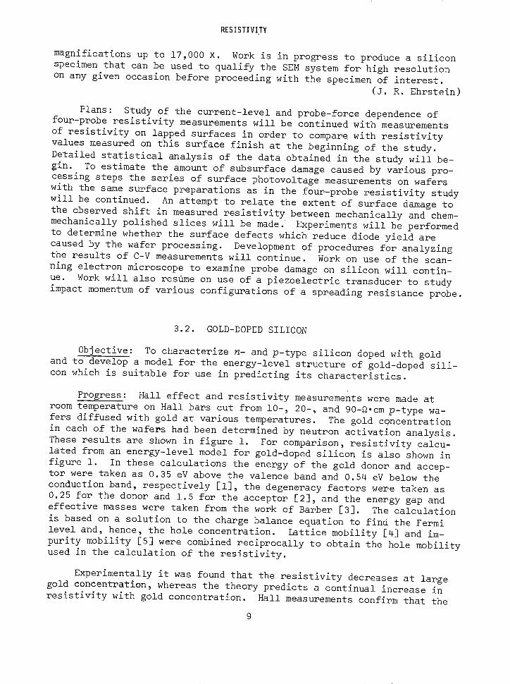
Progress: Hall effect and resistivity measurements were made atroom temperature on Hall bars cut from 10-, 20-, and 90-0.cm p-type wa-fers diffused with gold at various temperatures. The gold concentrationin each of the wafers had been determined by neutron activation analysis.These results are shown in figure 1. For comparison, resistivity calcu-lated from an energy-level model for gold-doped silicon is also shown infigure 1. In these calculations the energy of the gold donor and accep-tor were taken as 0.35 eV above the valence band and 0.54 eV below theconduction band, respectively [1], the degeneracy factors were taken as0.25 for the donor and 1.5 for the acceptor [2], and the energy gap andeffective masses were taken from the work of Barber [3]. The calculation
is based on a solution to the charge balance equation to find the Fermilevel and, hence, the hole concentration. Lattice mobility [4] and im-purity mobility [5] were combined reciprocally to obtain the hole mobilityused in the calculation of the resistivity.
Experimentally it was found that the resistivity decreases at largegold concentration, whereas the theory predicts a continual increase inresistivity with gold concentration. Hall measurements confirm that the
9
GOLD-DOPED SILICON
Figure 1. Resistivity as a function ofgold concentration in p-type silicon.(Error bars are not indicated. Thestandard deviation of the gold determi-nation is estimated to be about 10percent. Resistivity values are re- ,producible within about 5 percent).
2- / / Tr // 0
w, ,- / /
0c:
/ 0
102
/ Theory Exp./ I~10 a-cm o
~~~/ / 20 alcm ..90 -cm--- .
100 0
GOLD CONCENTRATION (atoms/cm 3 )
retrograde behavior is due to an increase in the charge carrier densityrather than an increase in the carrier mobility. A suitable model to ex-plain this behavior has not yet been found.
Gold diffusions were completed on sets of n-type wafers with initialroom temperature (230 C) resistivity of 5, 80, 400, and 2,200 -'cm. Thediffusion temperatures and times used were: 8500 C for 288 h, 9500C for144 h, 10500 C for 72 h, 11500C for 24 h, and 12500C for 8 h. Gold con-centrations were determined by activation analysis. Data on these andprevious sets of wafers indicate that the diffusion times at 1150 and12500C are long enough that the concentration of gold reaches the solubil-ity limit [6], but the times at the lower temperatures are not longenough for this to occur.
(W. R. Thurber, A. W. Stallings, T. F. Leedy, and W. M. Bullis)
A layer 5-pm thick was removed by lapping from the surface of theHall bar previously shown to have gold clusters by x-ray fluorescence(NBS Tech. Note 598, p. 13). In all regions, including those where clus-ters had been observed, the x-ray intensity of the gold peak did not ex-ceed the background level. This suggests either that the clusters do notextend as much as 5 pm below the surface or that the gold concentrationin a cluster decreases rapidly with distance below the surface.
(W. J. Keery and W. R. Thurber)
Preliminary measurements of carrier diffusion length were attemptedon gold-diffused Hall bars. Difficulties were encountered that can betraced to low signal levels; modifications to the equipment to overcomethese limitations were begun. (W. R. Thurber and W. E. Phillips)
10

GOLD-DOPED SILICON
Plans: A new specimen holder will be fabricated for room tempera-ture Hall effect and resistivity measurements. Improved means for main-taining and measuring the specimen temperature will be included. Elec-trical properties of the Hall bars cut from the 5-, 80-, 400-, and2 ,2 00-Q-cm n-type, gold-diffused wafers will be measured using the newholder. Sets of p-type wafers with room temperature (230 C) resistivitiesof 0.5, 1,000, and 2,000 Q-cm will be diffused with gold at five temper-atures from 850 to 12500 C.
To further study the retrograde behavior of the resistivity in p-type material, 10-Q-cm wafers will be diffused at 12500C for 8, 16, 32,and 64 hours. These times are all long enough for the gold concentra-tion to stabilize at its maximum solubility, but if foreign impuritiesare diffusing in, their concentration should increase with time andchange the measured resistivity.
Additional measurements of carrier diffusion length will be made bythe surface photovoltage method on the same Hall bars used for electricalmeasurements after.modifications to the equipment have been completed.
3.3. SPECIFICATION OF GERMANIUM
Objective: To measure the properties of germanium crystals and tocorrelate these properties with the performance of germanium gamma-raydetectors in order to develop methods for the early identification ofcrystals suitable for fabrication into lithium-compensated gamma-ray de-tectors.
Progress: Study of methods for measuring lithium-ion drift mobilityin germanium has been completed with the adoption by ASTM Committee F-1of a method based on technology developed under this task [1]. Work onmethods for measuring carrier trapping in germanium is continuing in co-operation with the committee. The improved infrared response techniquewas used to study eight germanium diodes- gold was identified in one thathad been doped to a concentration of 101 gold atoms per cubic centimeter.Application of the infrared response method to silicon devices continued.
Characterization of Germanium - Measurements of carrier trappinghave been completed on specimens from two germanium crystals. The pro-cedure used was that specified for the second round-robin being conductedin cooperation with the Germanium Section of Committee F-1. Detectorresolution was measured as a function of applied electric field using the1333-keV gamma ray of 60Co. The position (channel number) of the centerof the 1333-keV peak in the pulse-height spectrum was also determined asa function of bias; independent values of effective carrier lifetime inthe test specimens can be obtained from the results of the two measure-ments. An additional series of measurements was carried out using a col-limated beam of 662-keV gamma rays from 1 3 7Cs in order to calculate
11

SPECIFICATION OF GERMANIUM
values of carrier lifetime using a model for carrier trapping developed
in this laboratory [2] and compare them with the values obtained accord-ing to the round-robin procedure.
(W. J. Keery, H. E. Dyson, and A. H. Sher)
Germanium Detector Measurements - Detectors fabricated from specimens
of eight germanium crystals were examined by the infrared response (IRR)technique. IRR spectra obtained from three germanium diodes for the
energy range 0.5 to 0.7 eV using a 640-line per millimeter grating and a
1-mm thick germanium filter window are shown in figure 2. The spectrumof NBS-83-3, a lithium-drifted diode, is typical of germanium used for
fabricating good quality gamma-ray detectors of this type. The spectrumof NBS-112, a diode* fabricated from a specimen of high-purity germaniumwith an initial net donor concentration of approximately 7 x 10 cm- 3
is in general similar to that of NBS-83-3 except that structure is notobserved at either 0.50 or 0.52 eV. Since lithium compensation was not
used in the fabrication process (NBS Tech. Note 598, pp. 15-16) one would
not expect to observe the 0.50-eV level due to the lithium-defect inter-action. Structure in the region near 0.52 eV has been noted in all
lithium-drifted diodes; some of the defects responsible for this structure
apparently are not present in the high-purity crystals. The spectrum ofNBS-113, a diode* fabricated from a crystal of high-purity germanium in-
tentionally doped with approximately 1011 gold atoms per cubic centimeter,exhibits peaks at 0.57 and 0.66 eV. Gold introduces a donor level at anenergy of E + 0.05 eV, and acceptor levels at E + 0.15, E - 0.20 and
E - 0.04 e} in germanium [3]; the peaks in the spectrum can be relatedto the excitation of electrons from the donor level and the lowest accept-or level to the conduction band. These results demonstrate the high sen-sitivity of the IRR technique to the presence of gold in germanium.
Attempts were made by measurement of IRR to confirm the presence ofiron in NBS-301, fabricated from a germanium crystalt intentionally con-
taminated with stainless steel during growth from the melt. Levels in
germanium arising from iron impurity are at energies of E + 0.34 eV andE - 0.27 eV [3]. Observed broadening on the high energyVside of the0.36 eV peak might possibly be due to excitation of electrons from thelower iron level to the conduction band; however, because of the still un-known origin of peaks observed in germanium at 0.36, 0.24, and 0.18 eV,no definite conclusions can be drawn from the IRR data at present.
(A. H. Sher, W. J. Keery, and H. E. Dyson)
A study was carried out to determine the feasibility of obtaining IRRspectra in digital form for analysis by computer and ease of comparisonof spectral runs made at different settings. A method that involved use
Supplied by R. D. Baertsch, General Electric Company, Schenectady, N. Y. 12301.
t Supplied by I. L. Fowler, AECL Chalk River Nuclear Laboratories, Chalk River,Ontario, Canada.
12

SPECIFICATION OF GERMANIUM
Figure 2. Infrared response spectra of three germa-nium gamma-ray detectors.
0.66
NBS-113
0.57
NBS-83-3
NBRG S-1120
W
LU
0.5 0.6 0.7
ENERGY (eV)
of equipment currently on hand was found to be successful. The varyingvoltage output from the phase-sensitive amplifier is converted linearly toa variable frequency and fed to a miltichannel analyzer that is operatingin the multiscaling mode in which total counts occuring in a given timeinterval are stored in one channel. A switch mounted on the monochromatorgrating drive to give 100 closures per drum turn advances the analyzer ad-dress so that the recorded count is proportional to the IRR signal at anygiven energy. The IRR spectrum in digital form is then punched onto papertape and analyzed by a computer. (W. J. Keery and A. H. Sher)
Further efforts were made to apply the IRR technique to microelec-tronic devices (NBS Tech. Note 598, p. 16) by studying a 37-mil (0.94-mm)square silicon mesa diode mounted on the special right-angle holder at theend of the cryostat cold finger. Although considerable improvement insignal-to-noise ratio was obtained by using a 0.1-mm thick silicon filterand by replacing the 45-W light source with a 150-W light source, only theband-edge peak was observed. The present effort was also hampered by de-velopment of mechanical problems in the motorized monochromator gratingdrive. (W. J. Keery)
13

SPECIFICATION OF GERMANIUM
Plans: Emphasis will continue on the interpretation of results ob-tained using the improved IRR technique. Efforts to extend this tech-nique to silicon microelectronic devices will continue. As this efforthas been expanded to include silicon devices and detectors as well asthose of germanium, subsequent results will be reported in a section offuture quarterly reports devoted to infrared methods. The monochromatordrive mechanism will be repaired, the 100-closure per drum turn switchinstalled, and the monochromator recalibrated. Measurements of IRR onlithium-drifted silicon detectors subjected to electron and neutron radi-ation damage (see Section 5.5) will begin.
3.4. REFERENCES
3.1. Resistivity
1. Standard Method for Measuring Resistivity of Silicon Slices with a Collinear Four-Probe Array (ASTM Designation: F84-70), Annual Book of ASTM Standards, Part 8,(Available from American Society for Testing and Materials, 1916 Race St., Phila-delphia, Pa. 19103).
3.2. Gold-Doped Silicon
1. Collins, C. B., Carlson, R. 0., and Gallagher, C. J., Properties of Gold-Doped Sil-icon, Phys. Rev. 105, 1168-1173 (1957.).
2. Bullis, W. M, and Strieter, F. J., Electrical Properties of n-Type Silicon Dopedwith Gold, J. Appi. Phys. 39, 314-318 (1968).
3. Barber, H. D., Effective Mass and Intrinsic Concentration in Silicon, Solid-StateElectronics 10, 1039-1051 (1967).
4. Ludwig, G. W., and Watters, R. L., Drift and Conductivity Mobility in Silicon, Phys.Rev. 101, 1699-1701 (1956).
5. Brooks, H., Theory of the Electrical Properties of Germanium and Silicon, Advancesin Electronics and Electron Physics, L. Marton, ed. (Academic Press, New York,1955) Vol. VII, pp. 156-160.
6. Bullis, W. Mt., Properties of Gold in Silicon, Solid-State Electronics 9, 143-168(1966).
3.3. Specification of Germanium
1. To be published, November, 1971, as Method for Measuring Lithium-Ion Drift Mobilityin Germanium Single Crystals (ASTM Designation: F334-71T) Annual Book of ASTM Stan-dards, Part 8 (Am. Soc. for Testing and Materials, Philadelphia, Pa., 1971).
2. Sher, A. H., Carrier Trapping in Ge(Li) Detectors, IEEE Trans. Nucl. Sci. NS-18,No. 1, 175-183 (1971).
'. Neuberger, M., Germanium Data Sheets, Electronic Properties Information Center(EPIC) Report DS-143 (February, 1965); Available from National Technical Informa-tion Service, Springfield, Virginia 22151, Accession Number AD 610828.
14
4. METHODS OF MEASUREMENT FOR SEMICONDUCTOR PROCESS CONTROL
4.1. DIE ATTACHMENT EVALUATION
Objective: To evaluate methods for detecting poor die attachment insemiconductor devices with initial emphasis on the determination of theapplicability of thermal measurements to this problem.
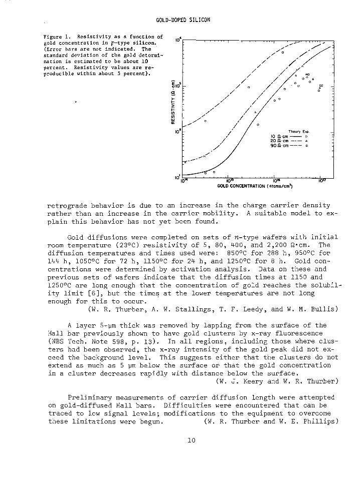
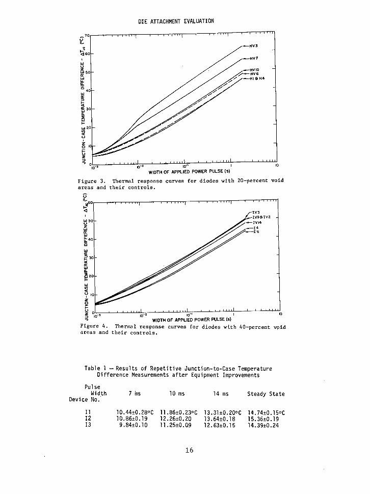
Progress: Measurements of steady-state and transient thermal re-sponse of diodes with various size voids reported previously (NBS Tech.Note 598, p. 20) indicated that the increase in sensitivity to voids ofthe transient thermal response measured for power pulses of 7 and 9 msover that of the steady-state thermal response ranged in most cases from90 to 700 percent. The data also indicated that although the spread inmeasured junction-to-case temperature difference, AT , was small fordevices with no intentional voids this was not the case with the inten-tionally voided devices. These conclusions are illustrated in figures 3and 4 which show transient thermal response curves for a representativesampling of devices. Curves denoted by the symbol HV or IV are for diodesthat had a void area introduced into the die attachment while curves de-noted by the symbol H or I are for control diodes without voids. Thevoided devices, series HV and IV, were bonded on gold-plated TO-5 headerswith 20- and 29-mil (0.51- and 0.74-mm) diameter dimples ultrasonicallymachined into the bonding surface (NBS Tech. Note 560, pp. 27-29) to pro-duce voids that are approximately 20 and 40 percent of the total chipbonding area, respectively. The results presented in these figures gen-erally confirm the anticipated thermal response behavior (NBS Tech. Note555, pp. 25-27). At heating-power pulse widths greater than about 10 to20 ms, the increase in AT due to poor die adhesion is essentially con-
JC.stant; the maximum sensitivity occurs for pulse widths of about 10 ms.The spread in thermal response of the devices with the 20-percent voidareas was significantly larger than in that of devices with 40-percentvoid areas. Radiographs and sectioning of both types of voided devicesindicated that the unbonded region around the smaller dimples was largerthan expected and varied from diode to diode, while better control was inevidence for devices with the larger dimples.
The die attachment evaluation equipment was modified to increase itspower handling capabilities and to increase the resolution of the digitalvoltmeter that indicates the forward voltage used as the temperature sen-sitive parameter. Long-term, single-operator measurements were made torecheck the reproducibility of the equipment. Over a period of 9 days,steady-state and transient thermal response for heating-power pulse widthsof 7, 10, and 14 ms were measured 12 times each on three commercial sili-con mesa diode chips bonded to TO-5 headers. The average value and samplestandard deviation of ATTC obtained for each measurement condition arelisted in table 1. The lzode heating current was 800 mA for the pulsedmeasurements and 300 mA for the steady-state measurements. In all cases
15
DIE ATTACHMENT EVALUATION
WIDTH OF APPLIED POWER PULSE (s)
Figure 3. Thermal response curves for diodes with 20-percent voidareas and their controls.
WIDTH OF APPLIED POWER PULSE (s)Thermal response curves for diodes with 4 0-percent voidtheir controls.
Table 1 - Results of Repetitive Junction-to-Case TemperatureDifference Measurements after Equipment Improvements
PulseWidth
Device No.7 mns 10 ms 14 ms Steady State
I1 10.44+0.28oC12 10.86±0.19I3 9.84±0.10
11.86±0.23oC12.26±0.2011.25±0.09
13.31±0.20oC13.64±0.1812.63±0.15
14.74±0.15oC15.36±0.1914.39±0.24
16
u60
<-
W 50O2wa:
L40
,D 30
L320
U
O0
2 -
, o-
Figure 4.areas and
Io

DIE ATTACHMENT EVALUATION
the forward voltage was measured 50 ps after termination of the heatingcurrent. The maximum sample standard deviations of ±0.28°C for the tran-sient thermal response measurements and ±0.24°C for the steady-state meas-urement were substantially lower than the values of ±0.54°0C and ±0.690°Cobtained before the circuit was modified (NBS Tech. Note 598, pp. 18-19).
Measurements of steady-state thermal response and transient thermalresponse for heating-power pulse widths ranging from 1 to 100 ms weremade on 10 diodes bonded to gold-plated TO-5 headers with 15-mil (0.37-mm)diameter dimples ultrasonically machined into the bonding surface and on10 control diodes with no intentional voids. This size dimple producesvoids that are approximately 10 percent of the total chip bonding area.The average steady-state thermal response and transient thermal responsefor a heating-power pulse width of 10 ms, measured on the control diodes50 ps after the termination of the heating pulse, were 15.53°C and12.010C, respectively. A heating current of 800 mA was used for the tran-sient response measurement while 300 mA was used for the steady-statemeasurement. The sample standard deviations in measured AT under steady-state and transient conditons were ±0.730 C and ±+0.90°C, respectively.This was significantly larger than was observed previously (NBS Tech.Note 598, pp. 19-20) on control devices associated with diodes having 20-and 40-percent void areas. For half of the diodes with voids, AT Cmeasured under transient conditions fell within the scatter obtained onthe controls, while the other half showed significantly larger values ofAT . Nevertheless, it can be asserted with 95 percent confidence [1]that the average of the thermal response readings for the diodes with 10-percent void area exceeds the average of the controls, although there isno reason to believe that the average of the steady-state temperature riseexceeds the average of the controls. It appears then, that a 10-percentvoid in the chip bonding area is the smallest size void that can be de-tected in this particular device using the transient thermal response tech-nique while a measurement of thermal resistance would not be sensitive tovoid areas this small. (F. F. Oettinger and R. L. Gladhill)
Plans: Measurements of steady-state and transient thermal responseon diodes with controlled void areas of various diameters will continue.Analysis of the accumulated steady-state and transient thermal responsedata for diodes with the various size voids and their controls will con-tinue. A study will also be undertaken to ascertain, theoretically, thelimitations of thermal response techniques for detecting poor die adhesionin the devices under investigation.
4.2. WIRE BOND EVALUATION
Objective: To survey and evaluate methods for characterizing wirebond systems in semiconductor devices and where necessary to improve exist-ing methods or develop new methods in order to detect more reliably thosebonds which eventually will fail.
17

WIRE BOND EVALUATION
Figure 5. SEM photomicrograph of typicalribbon-wire first bond. (Magnification350 x)
Figure b. SUM pnotomicrograph of typicalribbon-wire second bond. (Magnification390 X)
1
EOj
6.j.
20 /
Figure 7. SEM photomicrograph of overbondedribbon-wire first bond. (Magnification 400 X)
Figure 8. SEM photomicrograph of lift-offpattern of ribbon-wire first bond. (Magnifi-cation 350 X)
Figure 9. SEM photomicrograph of lift-offpattern of ribbon-wire second bond. (Magni-fication 350 X)
18

WIRE BOND EVALUATION
Progress: Work progressed on ribbon-wire bonding despite severalcontinuing problems with both the bonding machine and the dimensional uni-formity of the wire. Scanning electron microscope (SEM) photomicrographswere made of bonds and of lift-off patterns. Evaluation of the pull teston round-wire bonds was deferred due to serious mechanical problems withthe round-wire bonding machine. A simple technique for refinishing usedbonding tools was devised. Assistance in the organization of a sectionon microelectronic bonding was provided in conjunction with the summermeeting of ASTM Committee F-1 at NBS. More than 40 representatives ofdevice manufacturers, materials and equipment producers, and consumersattended. Ten areas in bonding were selected and task forces were setup to take the necessary action.
Ribbon-Wire Bonding - Limited work continued on the ribbon-wire bond-er received last quarter. Several problems remain to be solved beforeoptimum performance and reliability can be achieved. The most seriousproblem is that the bonding tool jumps straight up and bounces after thefirst bond is made. Such motion bends the wire at the heel, causing acrack which weakens the bond. Correction of this motion can only be ac-complished by designing a new transducer-motion cam. A considerable var-iation in bond tail length has also been observed. This must be con-trolled before the machine can be used to bond devices. In addition theavailable ribbon wire does not have uniform dimensions. The variationsobserved on a single spool of wire with cross-sectional dimensions 38 by12 pm were large enough to cause significant changes in bonding character-istics. Efforts were begun to determine if closer manufacturing toler-ances can be achieved.
SEM photomicrographs were made of several ribbon-wire bonds and lift-off patterns in order to understand the way such bonds are formed. Aphotomicrograph of a typical first bond made with normal power, time, andforce settings is shown in figure 5. The crack in the heel can be larglyattributed to the vertical jumping motion of the tool after the bond ismade. A photomicrograph of a typical second bond also made with normalsettings is shown in figure 6. The deformation for each bond is negligi-ble. Figure 7 shows a photomicrograph of a grossly overbonded first bondthat was made with twice the power setting of the bond in figure 5. Evenin this extreme case the deformation is only about 25 percent. This smalldeformation is assumed to be the reason why most ribbon bonds break in apull test at a tensile force in the wire of between 0.7 and 0.9 times thetensile strength of the wire, whether a heel crack is present or not.This is comparable with very good quality round-wire bonds (NBS Tech. Note598, p. 26). Photomicrographs of lift-off patterns of a first bond and asecond bond are shown in figures 8 and 9, respectively. Such patterns aremade by reducing the value of one or more bonding parameters, in this casethe power, below the point where the wire will stick to the pad. The bond-ing pattern is similar to those obtained for round-wire (NBS Tech. Note560, pp. 33-34); the main bonded area is around the perimeter of the bond.
19

WIRE BOND EVALUATION
As bonding progresses to the point that the wire will stick, the bondedarea extends inward toward the center. (H. K. Kessler)
Technique for PoZishing Bonding TooZs - A simple and convenient tech-nique for repolishing the bonding face of flat bonding tools has been de-vised. This technique requires no specialized equipment. A flat copperplate loaded with a diamond-bort paste is placed in the work stage of thebonding machine. The tool is lowered onto this polishing plate by adjust-ing the search-height control. The tool is polished by moving the workstage under the stationary tool in a general figure-eight pattern whilethe tool is applied with a force comparable with that used in bonding.During polishing, it is essential that the bonding tool be perpendicularto the diamond-loaded copper plate. The tool is removed and cleanedultrasonically before it is used for bonding. A preliminary evaluationof the method was carried out with diamond paste commerically specifiedas 3-pm particle size and by polishing for 1 min. This produced such ahighly smooth finish that the tool had to be broken in by making a numberof bonds at high power until the finish was slightly degraded. Use of acoarser diamond-bort paste should eliminate the need for this step.
(H. K. Kessler)
Standardization Activities - Considerable time was devoted to an or-ganizational meeting to form a new section of Subcommittee 7 of ASTM Com-mittee F-1 to develop standard test methods for microelectronic bonding.The purpose of the initial meeting was to identify areas in bonding wheremeaningful standards can be written, considering the present technology.More than 40 representatives of device manufacturers, materials and equip-ment producers, and consumers attended the meeting, chaired by K. 0. Leedy.Ten areas in bonding were selected for further investigation: the destruc-ive pull test, wire deformation, visual inspection, the temperature cycl-ing test, the air blast test, bonding wire specifications, bonding toolspecifications, tests for metallization adherence and bondability, testsfor beam-lead adherence, and a glossary of terms used in microelectronicbonding. Tests discussed but not chosen for further investigation at thistime include the non-destructive pull test, the centrifuge test, the ultra-sonic vibration test, the mechanical shock test, the shear test, and testsfor evaluating flip-chip bonds. Anyone interested in participating inthis activity should contact the chairman. (K. 0. Leedy and G. G. Harman)
Bibliography and CriticaZ Review - The bibliography was cleared forpublication as an NBS Technical Note [1]. Work on the final draft of thecritical survey paper continued. (H. A. Schafft)
Plans: Theoretical and experimental work on electronic mixing ofbonding tool ultrasonic signals will resume in the effort to better under-stand and control the bonding process. Advancement of the experimentalwork is contingent upon acquisition of specialized equipment. Attemptswill be made to secure ribbon-wire with closer dimensional tolerances andits evaluation for ultrasonic bonding will continue. Further work on the
20

WIRE BOND EVALUATION
wire indentation tester will be deferred until a suitable method for cal-ibration is found. Experimental and statistical analysis of significantfactors in the wire bond pull test will resume when the round-wire bonderis repaired and brought under control. Further assistance will be givento sponsors in connection with problems encountered on device productionlines. Cooperation with the newly formed Section on Microelectronic Bond-ing in Committee F-1 will continue with work on defining and evaluatingthe parameters of the destructive wire bond pull test. Efforts will bemade to coordinate this ASTM activity with associated activity in theSociety of Automotive Engineers and the Electronic Industries Association.The final draft of the critical survey paper will be completed and prepar-ed for publication as an NBS Technical Note. The preparation of a bibli-ography of limited distribution reports will be initiated.
4.3. PROCESSING FACILITY
Objective: To establish a microelectronics fabrication laboratorywith the facilities and procedures necessary for the production of special-ized silicon devices for use in research on measurement methods.
Progress: A process is being developed for fabricating diffused sil-icon diodes required by the resistivity task for the purpose of measuringthe resistivity as a function of depth in silicon bulk and epitaxial wa-fers by the capacitance-voltage method. The requirements of the diffusionare that its surface concentration be high (>1020 cm-3), that the junctionbe abrupt, and that the junction be shallow (<1 pm). Preparation of thediodes begins with the thermal oxidation of 1- to 10--.cm n-type wafers toa thickness of 0.5 pm to form a diffusion mask. Circular windows, 0.5 mmin diameter, are defined in the oxide with conventional photolithographictechniques. After cleaning, the wafer is diffused for 1 h with boron froma boron nitride source at 10500 C. Sections of the diodes are beveled andstained to verify the junction depth. Typically the sheet resistance is10 0/0, giving a surface concentration of approximately 6 x 10²⁰ atomsper cubic centimeter. Diodes prepared in this manner on l-0-cm wafershave exhibited breakdown voltages less than 20 V in contrast to an expect-ed value of 60 V. The origin of the low breakdown voltages is being in-vestigated in cooperation with the resistivity group (see Section 3.1).
Additional effort was expended attempting to improve the quality ofaluminum films produced by the electron beam evaporation system. A cryo-genic coil was installed in an unsuccessful attempt to getter the gas pro-duced during evaporation. The coil consisted of 5 turns of ¼-in. (6.2-mm)diameter copper tubing bent into a 16-inch (450-mm) diameter helix. Liq-uid nitrogen passed through the coil served as the refrigerent. No de-crease in pressure was noted as the coil was cooled. Efforts were alsohampered by leaks around the low temperature connectors.
(T. F. Leedy and J. Krawczyk)
21

PROCESSING FACILITY
Plans: Groups of diodes required by the resistivity task will befabricated in an attempt to determine where the defects originate. Aftereach step of the process a wafer will be withdrawn and etched in a pre-ferential etch to display the crystallographic damage induced by thatstep. Both commercially polished wafers and wafers from a crystal cutand polished in-house will be used.
In the future, fabrication work will be reported with the appropriatetask. This section on Processing Facility will not be included unlesssignificant inprovements or additions to the capabilities of the facilityhave been made.
4.4. REFERENCES
4.1. Die Attachment Evaluation
1. Natrella, M. G., Experimental Statistics, NBS Handbook 91 (August 1, 1963) pp.3-36 to 3-37.
4.2. Wire Bond Evaluation
1. Schafft, H. A., Wire Bond Electrical Connections- Testing, Fabrication and De-gradation- A Bibliography 1957-1971, NBS Tech. Note 593, to be published.
22

5. METHODS OF MEASUREMENT FOR SEMICONDUCTOR DEVICES
5.1. THERMAL PROPERTIES OF DEVICES
Objective: To evaluate and, if necessary, improve electrical measure-ment techniques for determining the thermal characteristics of semiconduc-tor devices.
Progress: Prototype circuits to measure transistor thermal resist-ance and common-emitter current gain in the common-base operating modewere designed and built. These circuits are much simpler than the common-emitter circuits used up to this point because it is not necessary to usespecial circuitry in the base lead to control the collector current. Inthe case of the current-gain measurement, the simplicity of the common-base circuit makes feasible a production-oriented current-gain screeningtechnique for hot-spot formation. In a comparison of the effectivenessof the use of base-emitter junction voltage as a screen for thermal insta-
bilities with that of the common-emitter current-gain it was found thatwhile both were sensitive to constricted hot-spots that exhibit thermalhysteresis the former was much less sensitive to the more amorphous, lessconstricted hot-spots that occur under higher current, lower voltage op-erating conditions. A study was undertaken to determine the pulse con-ditions under which a power transistor could be put into a constrictedoperating mode with thermal hysteresis. With repetitively pulsed collec-tor excursions, it was found that hysteresis occurred when the productof the-magnitude of the voltage pulse and the duty cycle was equal tothe steady-state voltage change required to initiate hysteresis from agiven collector voltage below the d-c hot-spot initiation voltage. Forsingly pulsed excursions from various collector voltages below the d-chot-spot initiation voltage it was found that, for a given pulse width,the combined d-c and pulsed voltage required to initiate hot-spots in-creased as the starting d-c collector voltage level was reduced.
Standardization Activities - The measurement procedure and data col-lection format were established for the preliminary round robin on thermalresistance being conducted in cooperation with JEDEC Committee JC-25 onPower Transistors. Fourteen test specimens were measured in accordancewith the prescribed test procedure and sent to the first of the 10 indus-try participants. (F. F. Oettinger and S. Rubin)
ThermaZ Resistance Methods - The study to compare other frequentlyused thermal resistance measuring methods with the common-emitter base-and-collector switching technique now under investigation (NBS Tech. Note598, pp. 33 -34) was continued. A prototype circuit to measure transistorthermal resistance, R0, in the common-base operating mode was designedand built. The simplified circuit diagrams in figure 10 show both thepreviously built common-emitter R0 measuring circuit and the newly design-ed and fabricated common-base R measuring circuit. In each case the tran-sistor Q1 is initially on, and the sample-and-hold unit is holding. In
23

THERMAL PROPERTIES OF DEVICES
Figure 10. Circuits for measur- W ing thermal resistance of tran-
sistors. 2 i ,tTUT
EL CLOCKPULSE
PULSE
a. Common-emitter
01
V,,
b. Common-base
the common-emitter circuit, the transistor Q3 is initially on and the tran-sistor Q4 is initially off so that only the IB servo is providing current
to the base of the transistor under test. In the common-base circuit, thetransistor Q2 is off and the diode Dl in the emitter lead is conducting.
In both cases when the 120-ps wide, 4-pps clock pulse is applied, the tran-sistor Q1 is turned off by means of the photo coupler, and the sample-and-hold unit samples the emitter-to-base voltage for approximately 1 ps at
the end of a 10-, 20-, 50-, or 100-ps delay. This delay in measuring the
temperature sensitive parameter is set by an external switch. In the
common-emitter circuit, the clock pulse also initiates a 4-ps delay, thenreverses the states of transistors Q3 and Q4 to turn the I servo off and
Bthe VB measuring current supply on for a period of 110 ps, after which
transistors Q3 and Q4 revert to their original state. In the common-base
circuit, the inverted clock pulse turns the transistor Q2 on, shorting
out the VEE supply and causing the diode D1 to become nonconducting sothat the only current across the emitter-base junction is the measuring
current controlled by VBB.
The common-base R measuring circuit does not require the base switch-ing logic which is used with the common-emitter configuration. Further,
when measuring transistors with betas of 50 or more, the change in collec-
tor current as the collector voltage is varied is usually less than 1 per-
cent; thus, the use of a constant-current servo in the base lead to control
the collector current is not necessary. Both circuits have heating current
and voltage capabilities of 0 to 2 A and 0 to 250 V, respectively.
24

THERMAL PROPERTIES OF DEVICES
Measurements of R8using both circuits were made on four 35-W,
triple-diffused, silicon power transistors. The results of these prelim-inary measurements, given in table 2, indicate that there is substantialagreement between the two techniques. Further studies are needed to de-termine the relative merits of the two techniques when the transistor un-der test is operated under a wide variety of operating conditions.
An attempt was also made to make common-base R measurements usingthe collector-base junction voltage as the temperature sensitive parameter.Problems were encountered with the sample-and-hold unit as well as withspurious signals affecting the voltage reading. A study was undertakento determine what corrective measures should be taken to solve these prob-lems. (F. F. Oettinger and S. Rubin)
Screen for Hot Spots - The use of d-c current gain, hFE, as an indi-cator for the formation of hot spots and thermal hysteresis in power tran-sistors has been discussed previously (NBS Tech. Note 520, pp. 49-52).In this technique, the base current, I , is measured as a function ofpower dissipated in the transistor while holding the collector currentand case temperature constant. Under these conditions h E is proportionalto the reciprocal of I
B. Hot-spot formation is indicated by a distinct
increase in IBwith increasing power. The increase may be abrupt, as with
constricted hot spots that exhibit thermal hysteresis, or more gradual, asmay occur under higher current, lower voltage operating conditions. Typi-cal examples are shown as solid curves in figure 11.
The effectiveness of the more commonly used base-emitter junctionvoltage, VBE, as a screen for thermal instabilities [1] was compared withthat of the base current. In the V technique, the junction voltage isBEmeasured as a function of transistor power under conditions of constantcollector current and case temperature. Typical results, shown as dashedcurves in figure 11, indicate that while V is sensitive to hot spotsthat exhibit thermal hysteresis it is relatzvely insensitive to the moreamorphous, less constricted hot spot that occurs under higher current,lower voltage operating conditions. On the other hand, the IB techniqueclearly indicates the formation of hot spots at high as well as low cur-rent levels.
The measurements described above were made in the common-emitter mode.Similar indications of the formation of hot spots and thermal hysteresisare obtained if IB is measured in the common-base configuration. By com-paring the common-emitter and common-base circuits, shown in figure 12 itcan be seen that, as was the case with the common-base Re measuring cir-cuit, the common-base hFE circuit does not require a constant-current servoin the base lead to control the collector current as the collector voltageis varied. It is therefore evident that a production-oriented screeningtechnique for hot-spot formation is feasible using the common-base hcircuit. (F. F. Oettinger and S. RubLn)
25
THERMAL PROPERTIES OF DEVICES
Table 2 - Comparison of Thermal Resistance Measuredusing Common-Emitter and Common-Base Circuits
Transistor0-600-610-620-69
Common-Emitter1.99oC/W1.721.65
.179
Common-Base2.OOoC/W1.771.761.77
Figure 11. Base current (solid curves)and base-emitter voltage (dashedcurves) as a function of power for asilicon power transistor showing onsetof hot spots.
a. Common-emitter b. Common-base
Figure 12. Circuits for measuring common- emitter current gain of transistors.
26
2.8
2.7
2.61
2.5
2.4
.E 2.3
Z 2.1
OI
U) 1.3
Ew
700 >
675 4_l0
655 >
625 .
600
575
550
1.2
I.1I
1.0
0.9 i -
4 8 12 16 20 24
POWER (W)28 32 36
_L

THERMAL PROPERTIES OF DEVICES
Thermal Hysteresis under Pulsed Operation - A study was undertakento determine the pulse conditions (voltage transients or surges) underwhich a power transistor would be put into a constricted operating modewith thermal hysteresis. Both singly and repetitively pulsed collector
excursions were performed with the common-base hFE circuit. The voltagepulses were generated by utilizing the collector-switching transistor nor-
mally used with the common-base Re measuring circuit to short out a vari-able resistor in the collector circuit of the transistor under test. Itwas determined from the singly pulsed measurements that the transistorwould go into thermal hysteresis if the collector voltage pulse had the
proper combination of magnitude and width for a given starting point be-low the hot-spot initiation voltage. For example, a 20-V pulse, 5-ms
wide caused a particular 35-W, triple-diffused, silicon power transistorto go into the constricted mode when the pulse was added to a d-c collector
voltage level 6 V below the hot-spot initiation voltage. When the d-c
collector voltage level was decreased to a point 12 V below the hot-spot
initiation voltage the 5-ms wide pulse had to be increased to 30 V to
cause a hot spot to form; a 10-V increase in pulse height is therefore
required for a 6-V decrease in d-c collector voltage level. This non-linear difference in energy needed to cause the device to go into thermal
hysteresis might be explained by the fact that as the device operating
point approaches the hot-spot initiation voltage it takes a proportionally
smaller amount of energy to produce the needed temperature gradient due
to that which already exists (NBS Tech. Note 592, pp. 49-51).
Work with repetitively pulsed collector voltage excursions demonstrat-
ed that hysteresis occurred when the product of the magnitude of the volt-
age pulse and the duty cycle equalled the steady-state change required to
initiate hysteresis from a given collector voltage below the hot-spot ini-
tiation voltage. This was evidenced most clearly by the action of a mov-
ing coil voltmeter that was used to read the collector voltage. The volt-
age magnitude at which the device went into thermal hysteresis as indicat-
ed by the meter was the same for a d-c collector voltage as for a combined
d-c and pulsed voltage. (S. Rubin and F. F. Oettinger)
Plans: The literature search and work on the bibliography on thermalresistance and transient thermal response measurements will be resumed.Design changes will be incorporated into the existing common-base R meas-
uring circuit to facilitate the use of the collector-base junction voltageas the temperature sensitive parameter for transistor thermal resistancemeasurements. Comparison of measurements made with this and other tech-
niques for measuring R will then be made. Work will also continue on thedetermination of the thermal inertia characteristics of the thermal hyster-esis phenomenon. Thermographic measurements will be made on devices toinvestigate the relationships which may exist between the peak temperatureon the chip and the electrically measured junction temperature.
27

5.2. THERMOGRAPHIC MEASUREMENTS
Objective: To evaluate the utility of thermographic techniques fordetection of hot spots and measurement of temperature distribution insemiconductor devices.
Progress: An improved heat sink was fabricated to facilitate thecalibration of the temperature sensitivity of the phosphors. The heatsink is suitable for calibrations in the temperature range 20 to 315°Cwhich includes the temperature range of the three lowest temperature phos-phors and the lower end of the temperature range of the highest tempera-ture phosphor.
Further work was done with a slurry-settling technique for coating aspecimen with phosphor. In this technique the specimen is placed in aslurry composed of 0.45 to 0.9 g of phosphor in 60 cm3 of ethyl alcoholand the phosphor is allowed to settle onto the specimen surface for sever-al minutes. The slurry is then drained and the specimen allowed to dryfor 1.5 to 2 h while it is protected from air currents and kept at approx-imately room temperature. Preliminary results suggest that the thicknessof the phosphor coating thus obtained can be controlled by controllingthe depth beneath the surface at which the specimen is placed or by con-trolling the phosphor concentration in the slurry. The slurry-settlingtechnique appears to give a more uniform phosphor coating than the water-floatation technique (NBS Tech. Note 488, p. 31), but conclusive experi-ments have yet to be made.
It was determined that the microcopy resolution chart (NBS Tech. Note592, p. 56) used to establish the spatial resolution of the fiber-opticprobe does not have strictly well defined white and black lines. Uponviewing the charts under a microscope (approximately 300 X magnification)a gray transition region between the black and white lines can be seen.The gray region consists of black dots randomly spaced on a white field;the density of dots decreases toward the center of the white line. Forthe smallest line width available on the test chart (0.028 mm), the dotsextend across the entire width of the white line. This gray region mayaccount for the apparently poor agreement between the spatial resolutionof the 50-pm fiber-optic probe as determined with the aid of the microcopyresolution charts and the spatial resolution stated by the manufacturer.It has not yet been established whether it is possible, by accounting forthe gray region, to determine the resolution of the fiber-optic probe bymeans of these charts.
Silicon wafers with surfaces of silicon dioxide, aluminum, gold, chro-mium, and polished silicon have been obtained for use in a study to estab-lish coating uniformity and to determine whether a reaction occurs betweenthe phosphors and the various surfaces.
(D. L. Blackburn and L. R. Williams)
Plans: The temperature calibration of the phosphors coated by thepreviously used water-floatation technique will be concluded. The proce-
28

THERMOGRAPHIC MEASUREMENTS
dure for coating wafers and devices by the slurry-settling technique willbe further developed to allow a controlled coating thickness to be obtain-ed. If it is not feasible to use the microcopy resolution charts to es-tablish the spatial resolution of the fiber-optic probe, metallizationstrips on a silicon substrate will be tested for this determination. Cal-ibration and temperature sensitivity measurements on specimens coated bythe slurry-settling technique will begin. Measurements will be made toestablish the comparative uniformity of coatings made by the water-floatation and slurry-settling methods.
5.3. MICROWAVE DEVICE MEASUREMENTS
Objective: To study the problems and uncertainties associated withthe measurement of selected microwave device properties, and to improvethe techniques of these measurements.
Progress: To improve the precision of the low intermediate-frequency conversion-loss measurements, an incremental modulation tech-nique has been introduced. With this technique, precision is limitedprincipally by the resolution of the attenuator used to set the incrementand by the mechanical stability of the waveguide system rather than by
the output resolution.
In the new arrangement, the square-wave a-f generator used to modu-late the local oscillator has been replaced by a stable d-c power supply.The change in r-f power caused by this d-c supply can be made identicalto that caused by the square-wave generator. As before, power calcula-tions are based upon sinusoidal modulation yielding the same peak andtrough values. In effect, this change to incremental modulation reducesthe intermediate frequency to zero. In addition to the advantage ofusing a more stable modulation source, this change also allows the useof a narrower signal bandwidth, which reduces system noise. It also al-lows the use of the precision rotary-vane attenuator, currently used tocalibrate the PIN modulator, directly as the incremental modulator it-self. A further advantage of incremental modulation is that the outputvoltage "peaks" can be read directly on a digital voltmeter, rather thanby the more complex, less precise switched-oscilloscope d-c comparisonmethod used with a-f modulation.
Incremental modulation has been used in the past for absolute mixerconversion loss measurements of the highest accuracy. As this method hasbeen used [1], a microammeter is used to read an output current incrementthat occurs with an incremental change in power. The equation used toconvert the current increment to conversion loss was not based on the
modulation concept. In developing the periodic modulationpmethod, common-ly known as the modulation method, as an absolute rather than a relativemethod, it has become apparent that the incremental modulation method,
29
MICROWAVE DEVICE MEASUREMENTS
commonly known as the incremental method, remains the superior techniquefor high precision measurements. Now, however, the availability ofprecise digital voltmeters makes a method based on a voltage incrementpreferable to one based on a current increment. The equation used toconvert the voltage increment is based on the modulation concept; thisequation can be shown to be equivalent to the earlier one used withmeasurements of current increment.
Using a table of attenuation as a function of vane angle [21, it wascalculated that the 0.0001-inch (2.5-pm) resolution of ordinary verniermicrometer heads used as adjustable stops to position the rotary-vane at-tenuator at precise locations should contribute less than 0.01 dB uncer-tainty to the conversion loss measurement. To obtain a commensurate ac-curacy, however, requires calibration of the attenuator to ±0.001 dB fora 1 dB modulation increment, which is several times better than can pre-sently be obtained. Preliminary consideration was given to the use of aprecision r-f power meter to establish the increment. To determine the.increment within an uncertainty of ±0.001 dB requires independent powermeasurements within an uncertainty of ±0.0005 dB or ±0.01 percent of thepower level. This is within the total bridge uncertainty (substitutedd-c power, exclusive of voltmeter) of ±0.0061 percent reported [3] forthe NBS Type II Power Measurement System for measurement of a power levelof 10 mW using a 200-Q, -12.3-Q/mW thermistor. Bolometer instability ap-pears likely to severely degrade this small uncertainty, so it is question-able that the use of a power meter to establish the increment would proveto be superior to the use of a calibrated attenuator. If the power meterwere, in fact, superior, this would suggest that the attenuator calibra-tion would be improved by using the same power meter.
An immediate limitation on precision is a lack of rigidity in thewaveguide system. It was observed that the r-f power to the mixer is af-fected by mechanical forces on the waveguide. There is sufficient hyster-esis in these power changes to suggest that interchanging the bolometer(mount) and the mixer (holder) or removing and reinserting a diode wouldresult in a significant permanent power change. Although power changesmay also result because of lack of reproducibility of diode contacts andposition and of waveguide flange connections, these aspects of the problemcannot be investigated until the waveguide system is made more rigid.
(J. M. Kenney)
Plans: To facilitate use of the precision attenuator as the incremen-tal modulator, it will be modified by the addition of precise mechanicalstops (vernier micrometer heads with locks), a modification that is alsorequired in order to improve the calibration accuracy beyond that possibleusing the relatively coarse dial. It will then be sent to NBS Boulder forcalibration.,1 A support system to add rigidity to the waveguide will bedeveloped. A review of the current status of measurement requirementsfor microwave mixers will be undertaken to assure that task goals continueto be appropriate to these needs.
30
5.4. CARRIER TRANSPORT IN JUNCTION DEVICES
Objective: To improve methods of measurement for charge carriertransport and related properties of junction semiconductor devices.
Progress: The vector-voltmeter measurement system for measuring tran-sistor delay time was assembled and preliminary tests were carried out.Two systems for the measurement of transistor S-parameters in the 200 to800 MHz range are being assembled. An analysis of the equivalent circuitsof a transistor in the Sandia-type bridge and in the vector-voltmeter cir-cuit has been made to relate the measured delay time to various time con-stants and delay times within the device.
Experimental - A delay-time measurement circuit was constructed tointerface between the transistor under test and a vector voltmeter. Thisallows measurements made using the Sandia-type bridge to be compared withthose made using the completely independent, vector-voltmeter system.Preliminary measurements made with the vector-voltmeter on a siliconn-p-n transistor with f of about 350 MHz yielded delay times which wererelatively independent of measurement frequency, as they should be, overthe range 3 to 30 MHz. In order to resolve questions of absolute accura-cy, a tiny R-C network of known delay time (423 ps) was assembled on aTO-18 transistor header. A spot measurement at 13 MHz on this networkin the transistor socket yielded a measured delay time of 460 ps. Thisis within the specified accuracy of the vector voltmeter; greater accura-cy requires the use of more refined techniques for calibration that arenow being developed. The present approach is derived from the R-C net-work plug-in idea, and uses networks of known phase shift to calibratethe vector voltmeter to the accuracy needed for the transistor measure-ments. (D. E. Sawyer and F. R. Kelly)
Two systems are being assembled for the measurement of transistor S-parameters in the 200 to 800 MHz range. In both systems the r-f sourceis coupled to the transistor under test through a dual directional couplerand provisions are made to measure the amplitide and phase of both the sig-nal reflected from the transistor terminals and the signal transmitted bythe transistor. One system, being obtained commercially, is self-containedand requires only a bias supply and connections to the signal source andthe device being measured. The second system is being assembled of indi-vidual components to provide an independent check on measurements madewith the first. (G. J. Rogers)
AnaZyticaZ - The equivalent circuits of a transistor in the Sandia-type bridge and in the common-base delay-time measurement circuit basedon the use of a vector voltmeter have been analyzed to relate the measureddelay time to the various time constants and delay times within the device.With the generally applicable measurement condition wT << 1 prevailing,where w is the test angular frequency and T the delay time obtained fromthe vector voltmeter, the transistor delay time expression simplifies to
T = Ir + - /hvv a e c fe
31

CARRIER TRANSPORT IN JUNCTION DEVICES
In this equation T is the delay time due to the transit of minority car-
riers across the base and collector junction regions, T = r C , and
.c = rC , where r is the small-signal emitter-base input resistance, rb
is the base resistance, C and C are the emitter-base and base-collector.e c
transition-region capacitances, respectively, and h is the common-
emitter small-signal current gain. Analysis of thefeandia-type bridge
yields a similar delay-time equation except that correction factors appear
as a consequence of the fact that for this bridge the signals applied to
the transistor are obtained from quasi-voltage sources, and not from cur-
rent sources, and so the transistor bridge input currents depend on the
values of the transistor elements such as r and rB. A memorandum is be-
e B.ing written to record all the details of the analysis of these two measure-
ment circuits so that applicable delay-time expressions can be obtained
for a wide range of measurement conditions.
In considering the delay-time error that might be introduced into
measurements made on the Sandia-type bridge by moving the primary loop in
the attenuator and phase-splitter box relative to the two secondary coils
(NBS Tech. Note 598, p. 40), it was concluded that this would not be adominant source of error under present conditions of measurement.
(D. E. Sawyer)
Plans: Techniques for rapid, and accurate calibration of the Sandia-type bridge and the vector-voltmeter delay-time measurement equipment willbe investigated. The memorandum relating measured delay times with deviceinternal processes will be completed. Two systems for the measurement ofdelay time by means of S-parameter measurement will be set up. Measure-ments on the same transistors will be made by all four methods and the re-sults compared.
5.5. SILICON NUCLEAR RADIATION DETECTORS
Objective: To conduct a program of research, development, and deviceevaluation in the field of silicon nuclear radiation detectors with empha-sis on the improvement of detector technology, and to provide consultationand specialized device fabrication services to the sponsor.
Progress: The studies of radiation damage effects of 600-keV elec-trons and fast neutrons in lithium-drifted silicon detectors have beencompleted. The effects of exposure of a silicon surface-barrier detectorto dry ammonia and methanol vapor at various pressures have been studied.
Testing and EvaZuation - Testing of commercial lithium-drifted sili-con detectors for evaluation before acceptance by the sponsor has beenconcluded. These pre-flight bench-tests were carried out at the NASA-GSFCsite for the IMP-H and Pioneer-F programs. (A. J. Baroody)
32

SILICON NUCLEAR RADIATION DETECTORS
Radiation Damage - A commercial, 2-mm thick, lithium-drifted silicondetector was irradiated with 600-keV electrons at fluences between 1 x 10¹²and 5 x 1015 cm- 2 on the particle entrance window (p-contact). The irra-diation was carried out at room temperature and with an applied detectorbias of 400 V. The average range of electrons of this energy in siliconis approximately 850 pm; therefore, defects are expected to be localizedin the region extending from the entrance window to a depth of approximate-ly 640 Pm [1]. Damage effects similar to those observed using 1.5 meVelectrons were seen (NBS Tech. Note 598, pp. 41-42), but to a lesser ex-tent. After irradiation at a fluence of 5 x 1015 cm -2 , a dead layer ap-proximately 600 pm thick was observed at a bias of 400 V at the irradiatedp-contact. No change in detector response was observed when counting par-ticles incident on the unirradiated rear contact.
A second detector was irradiated through the rear n-contact under thesame conditions as above. The results indicated that the increase ofnoise with increased fluence was much faster than that obtained from frontp-contact irradiation while the variation in current was about the same.
Two detectors were irradiated at room temperature with fast neutronsfrom a calibrated plutonium-beryllium neutron source. One detector wasreverse-biased at 400 V; the other, at 100 V. With the detectors located5 cm from the source, the neutron flux is approximately 5 x 104 cm-2 s- 1
.
The gamma-ray background was small and damage effects due to gamma rayscould be neglected. Fast neutron irradiation produces many secondary in-teractions in silicon because the energy acquired by the silicon atomsfrom elastic neutron collisions is quite high. Dearnaley [2] has estimat-ed that each neutron-silicon atom collision produces a minimum of 150Frenkel pairs. Such interactions are characterized by small, highly-damaged regions of complex defect clusters separated by considerableamounts of undamaged material due to the large mean free path between col-lisions. The degradation of detector performance observed due to neutrondamage was similar to that observed in the charged particle irradiationswith significant increases in noise and current above fluences of1010 cm-2 . After the final irradiation at a neutron fluence of approxi-mately 6 X-101 0 cm - 2, a dead layer of about 40 pm was evident on the ir-radiated front contacts of both detectors. This result indicates that thepulse-height defect was relatively independent of bias. The increase innoise and current with increased fluence was faster at the higher bias.Annealing effects have not been observed during a two week period follow-ing the irradiation. (Y. M. Liu)
Ambient Exposure Tests - The effects of exposure of dry ammonia andmethanol vapor on the noise of a silicon surface-barrier detector weremeasured. The detector was placed in the vacuum manifold and pumped at0.06 mTorr for 24 hours before dry ammonia was admitted into the testchamber. The detector noise level as measured using an oscilloscope andRMS voltmeter [3] varied from 33.5 to 39.7 keV before the tests were be-gun.
33

SILICON NUCLEAR RADIATION DETECTORS
Dry ammonia was leaked into the system through a variable micro-leak
valve and unless otherwise noted, the system was maintained at pressure
for 5 min before noise level measurements were made. Four measurementswere made at pressures from 0.03 to 0.7 mTorr; detector noise remained
fairly constant at 39.1 keV. Twenty measurements were made at pressures
from 1 to 100 mTorr; noise varied from 39.3 keV to 40.9 keV. The ammonia
pressure was held at 5 mTorr for 2 h; noise varied between 39.3 to 40.1 keV.
At the end of the 100 mTorr run, the pressure was lowered to 50 mTorr and
held there for 17 h; the noise level of the detector changed from 40.1 to
37.7 keV. The system was then pumped down to 0.03 mTorr overnight, and
tests were subsequently made from 100 to 1000 mTorr in six steps, holding
for 5 min at each step. The noise level remained near 36.9 keV.
Methanol exposure tests were run in a manner similar to the ammoniaruns. The spectro-grade methanol source consisted of a reservoir of the
solvent fed directly to the face of the leak valve. Ten measurements
were made at pressures ranging from 0.05 to 100 mTorr; detector noise
levels ranged from 36.2 to 36.9 keV. The pressure was held at the 1000
mTorr level for 2 h with no change in noise. (W. K. Croll)
Plans: The study of 2-MeV proton radiation damage effects in lithium-drifted silicon detectors will be completed. Detectors irradiated withelectrons, neutrons, and protons will be studied by means of the infraredresponse technique in order to seek correlation between the results ob-
served and energy levels introduced into the silicon by irradiation. Am-bient exposure tests will be carried out on lithium-drifted silicon de-tectors supplied by the sponsor. Dry ammonia, methanol, and commericalleak detector fluid will be used.
5.6. REFERENCES
5.1. Thermal Properties of Devices
1. Scarlett, R. M., Shockley, W., and Haitz, R. H., Thermal Instabilities and HotSDots in Junction Transistors, Physics of FaiZure in EZectronics, M. F. Goldbergand M. Vaccaro, Eds. (Spartan Books, Inc., Baltimore, Md., 1963), pp. 194-203.
5.3. Microwave Device Measurements
1. Method 4101.3, Conversion Loss, Test Method A (Incremental), MIL-STD-750B, TestMethods for Semiconductor Devices, Notice 1, 13 May 1970.
2. Larson, W., Table of Attenuation as a Function of Vane Angle for Rotary-Vane At-
tenuators (A = -40 log1 0 cos 8), NBS Tech. Note 229 (Jan. 7, 1965); see also Larson,W., Table of Attenuation Error as a Function of Vane-Angle Error for Rotary VaneAttenuators, NBS Tech. Note 177 (May 20, 1963).
3. Design Package Available for NBS RF Power Measurement System, NBS Tech. News BuZZ.
55, 117 (1971).
34

REFERENCES
5.5. Silicon Nuclear Radiation Detectors
1. Liu, Y. M., and Coleman, J. A., Electron Radiation Damage Effects in SiliconSurface-Barrier Detectors, IEEE Tracns. NucZ. Sci. NS-18, No. 1, 192-199 (1971).
2. Dearnaley, G., and Northrop, D. C., Semiconductor Counters for Nuclear Radiations,(E. 6 F. N. Spon Ltd., London, 1964), pp. 268-269.
3. USA Standard and IEEE Test Procedure for Semiconductor Radiation Detectors (forIonizing Radiation), USAS N42.1(1969)/IEEE No. 300, pp. 5-6.
35

Appendix A
JOINT PROGRAM STAFF
Coordinator: J. C. FrenchConsultant: C. P. Marsden
Semiconductor Characterization Section(301) 921-3625
Dr. W. M. Bullis, Chief
A. J. Baroody, Jr.F. H. BrewertM. CosmanDr. J. R. Ehrstein
R. L. MattisDr. W. E. PhillipsMiss D. R. Ricks
H. A. SchafftA. W. StallingsMrs. M. L. Stream+W. R. Thurber
Semiconductor Processing Section(301) 921-3541
Dr. A. H. Sher, Acting ChiefX
H. A. BriscoeW. K. CrollMrs. S. A. Davis+H. E. Dyson*G. G. Harman
W. J. KeeryH. K. KesslerJ. KrawczykT. F. Leedy
Y. M. LiuMiss J. M. MorrisonMrs. E. A. Simmons$L. M. SmithG. P. Spurlock
Electron Devices Section(301) 921-3622
J. C. French, Chief
D. L. BlackburnMrs. C. F. Bolton+Miss B. S. Hope+R. L. GladhillF. R. Kelly$
J. M. KenneyMrs. K. O. Leedy§Miss C. A. Main§F. F. Oettinger
M. K. PhillipsG. J. RogersS. RubinD. E. SawyerL. R. Williams
* Part Timet On Leave+ Secretaryi Summerx Dr. J. A. Coleman is on temporary assignment to Office of Associate
Director for Programs.§ Telephone: (301) 921-3625
36
Appendix B
COMMITTEE ACTIVITIES
ASTM Committee F-1 on ElectronicsA. J. Baroody, Lifetime SectionC. F. Bolton, Committee Assistant SecretaryW. M. Bullis, Editor, Subcommittee 4, Semiconductor Crystals, and
Subcommittee 7, Hybrid Microelectronics; Leaks, Resistivity,Mobility, Dielectrics, and Compound Semiconductors Sections
J. A. Coleman, Secretary, Subcommittee 5, Semiconductor ProcessingMaterials
J. R. Ehrstein, Chairman, Resistivity Section, Epitaxial Resistivity,and Epitaxial Thickness Sections
J. C. French, Committee EditorG. G. Harman, Bonding SectionK. 0. Leedy, Chairman, Bonding SectionT. F. Leedy, Photoresist SectionC. P. Marsden, Committee SecretaryR. L. Mattis, Lifetime SectionW. E. Phillips, Chairman, Lifetime Section; Secretary, Subcommittee
4, Semiconductor Crystals; Crystal Perfection, Encapsulation,Thin Films, and Thick Films Sections
A. H. Sher, Germanium SectionW. R. Thurber, Mobility, Germanium, Compound Semiconductors, and
Impurities in Semiconductors Sections
ASTM Committee E-10 on Radioisotopes and Radiation EffectsW. M. Bullis, Subcommittee 7, Radiation Effects on ElectronicMaterialsJ. C. French, Subcommittee 7, Radiation Effects on Electronic
Materials
Electronic Industries Association: Solid State Products Division, JointElectron Device Engineering Council (JEDEC)J. M. Kenney, Microwave Diode Measurements, Committee JC-21 on UHF
and Microwave DiodesF. F. Oettinger, Chairman, Task Group JC-11.3-1 on Thermal Con-
siderations for Microelectronic Devices, Committee JC-ll onMechanical Standardization; Technical Advisor, Thermal Resis-tance Measurements; Committees JC-22 on Thyristors, JC-20 onSignal Diodes, JC-Z5 on Power Transistors, and JC-30 on HybridIntegrated Circuits
S. Rubin, Chairman, Council Task Group on Galvanomagnetic DevicesH. A. Schafft, Technical Advisor, Second Breakdown and Related
Specifications, Committee JC-25 on Power Transistors
IEEE Electron Devices Group:J. C. French, Standards CommitteeJ. M. Kenney, Chairman, Standards Committee Task Force on Microwave
Solid State Devices II (Mixer and Video Detector Diodes)
37

APPENDIX B
H. A. Schafft, Chairman, Standards Committee Task Force on SecondBreakdown Measurement Standards
IEEE Nuclear Science Group:J. A. Coleman; Administrative Committee; Nuclear Instruments and
Detectors Committee; Editorial Board, Transaction on NuclearScience
IEEE Magnetics GroupS. Rubin, Chairman, Galvanomagnetic Standards Subcommittee
IEEE Parts, Hybrids, and Packaging GroupW. M. Bullis, New Technology Subcommittee, Technical Committee on
Hybrid Microelectronics
Society of Automotive EngineersJ. C. French, Subcommittee A-2N on Radiation Hardness and Nuclear
SurvivabilityW. M. Bullis, Planning Subcomm-.ttee of Committee H on Electronic
Materials and Processes
IEC TC47, Semiconductor Devices and Integrated Circuits:S. Rubin, Technical Expert, Galvanomagnetic Devices; U. S. Special-
ist for Working Group 5 on Hall Devices and MagnetroresistiveDevices
NMAB ad hoc Committee on Materials and Processes for Electron DevicesW. M. Bullis
NMAB ad hoc Committee on Materials for Radiation Detection DevicesD. E. Sawyer
38

Appendix C
SOLID-STATE TECHNOLOGY g FABRICATION SERVICES
Technical services in areas of competence are provided to other NBSactivities and other government agencies as they are requested. Usuallythese are short-term, specialized services that cannot be obtainedthrough normal commercial channels. Such services provided during thelast quarter are listed below and indicate the kinds of technology avail-able to the program.
1. Radiation Detectors (W. K. Croll and J. Krawczyk)Five lithium-drifted silicon detectors measuring 50 by 20 by0.75 mm and divided by 0.38 mm wide ultrasonically-machinedslots into 12 parallel active regions measuring 46 by 1.5 mmwere fabricated for the Electronuclear Physics Section foruse in an electron-scattering hodoscope.
2. Thin-Film Deposition (T. F. Leedy)Thin-film silver contacts were vacuum evaporated on piezo-electric polymer sheets for the Instrumentation ApplicationsSection.
3. Capacitor Fabrication (T. F. Leedy)Three quartz guard ring capacitors were fabricated for thePressure Measurements Section. Each capacitor consisted ofa quartz disc 1.5 cm in diameter by 2 mm thick. Aluminumcontacts were applied to each face and the edge. Guardrings were photolithographically defined in the faces of thedisc so that three-terminal capacitance measurements can bemade.
39

Appendix D
JOINT PROGRAM PUBLICATIONS
Prior Reports:
A review of the early work leading to this Program is given inBullis, W. M., Measurement Methods for the Semiconductor Device Industry-A Review of NBS Activity, NBS Tech. Note 511, December, 1969.
Quarterly reports covering the period since July 1, 1968, have beenissued under the title Methods of Measurement for Semiconductor Mate-rials, Process Control, and Devices. These reports may be obtained fromthe Superintendent of Documents (Catalog Number C.13.46:XXX) where XXXis the appropriate technical note number. Microfiche copies are avail-able from the National Technical Information Service (NTIS), Springfield,Virginia 22151.
Quarter Ending NBS Tech. Note Date Issued NTIS Accession No.
September 30, 1968December 31, 1968March 31, 1969June 30, 1969September 30, 1969December 31, 1969March 31, 1970June 30, 1970September 30, 1970December 31, 1970March 31, 1971
Current Publications:
Rubin S., and Oettinger,Effect on Restriction ofTransistors, IEEE Trans.
472475488495520527555560571592598
December, 1968February,.1969July, 1969September, 1969March, 1970May, 1970September, 1970November, 1970April, 1971August, 1971October, 1971
AD 681330AD 683808AD 692232AD 695820AD 702833AD 710906AD 118534AD 719976AD 723671AD 728611
F. F., Thermal Hysteresis and its Possiblethe Hot-Spot Free Operating Range of Some PowerElectron Devices ED-18, 393-394 (June, 1971).
Harman, G. G., and Kessler, H. K., Application of Capacitor Microphonesand Magnetic Pickups to the Tuning and Trouble Shooting of MicroelectronicUltrasonic Bonding Equipment, NBS Tech. Note 573, April, 1971.
Sher, A. H., and Thurber, W. R., Minority Carrier and Lithium-Ion DriftMobilities and Oxygen Concentration in p-Type Germanium, to be publishedin J. AppZ. Phys. (September, 1971).
Sher, A. H., Croll, W. K., and Thurber, W. R., Determination of Oxygen inGermanium Below 20 ppb by Measurements of Lithium Mobility and Precipi-tation, to be published in Anal. Chem. (November, 1971).
Brenner, D. J.,,* A Technique for Measuring the Surface Temperature of Tran-sistors by Means of Fluorescent Phosphor, NBS Tech. Note 591, July, 1971.
* NBS Measurement Engineering Division
40

APPENDIX E
STANDARDIZATION AND DISSEMINATION ACTIVITIES
(A summary for fiscal year 1971)
STANDARDS ACTIVITIES:
Interim standards
- ASTM editorial review (15 documents)
- Verification of standards
- Round robin experiments
ASTM (F-1) 5 methodsEIA (JEDEC: JC-22, 25) 3 methods
- Committee participation
ASTM (F-1, E-10)EIA (JEDEC: JC-1ll, 20, 21, 22, 24, 25, 30)IEC (TC-47)IEEE (G-ED, MAG, MTT, NS, PHP)NMABSAE (A2N, H)
About 20 staff members activeAbout 15 offices held by staff membersOver 50 task forces or committees attended
Benefits are (1) guidance to program, (2) rapid utilization ofresults by industry
FIELD VISITS: 54 to industrial, university, and government installations
PUBLICATIONS AND TALKS: 22; in addition QPR's go by request to nearly600 persons on initial distribution
VISITS TO NBS: About 75 formal; 105 for specific information exchange
CONSULTATIONS: 170
41
FORM NBS.114A (1-71)
U.S. DEPT. OF COMM. 1. PUBLICATION OR REPORT NO. 2 Gee 3. Recipient's Accession No.BIBLIOGRAPHIC DATA NO.
SHEET NBS-TN 702 _4. TITLE AND SUBTITLE 5. Publication Date
Methods of Measurement for Semiconductor Materials, Process November, 1971Control, and Devices. Quarterly Report, April 1 to June 30, 6.Per'rmincgrganizutoniC1971 "
7. AUTHOR(S) .8. Performing Organizain4 :W. Murray Bullis, Editor
9. PERFORMING ORGANIZATION NAME AND ADDRESS 10. Proiect/Task/Work Unit No.
NATIONAL BUREAU OF STANDARDS See Ttem 15DEPARTMENT OF COMMERCE 11. Contract/Grant No.WASHINGTON, D.C. 20234
See Item 12
12. Sponsoring Organization Name and Address NBS, DASA (EA071-801), Navy 13C Type of Report & PeriodCovered Interim April 1Strategic Systems Project Office, NAD, Crane, Indiana to June 30, 1971(PO-1-0030, PO-1-0041, and PO-1-0067), NAFI (WR-1-1038), NAVELEX 1 v(PO-1-1057), AFWL (F29601-71-0002), AFCRL (Y71-906), ARPA 14.SponsoringAgencyCo(MIPR FY76167100331), AEC, NASA (S-70003-G and H-76553A); : : __
15.SUPPLEMENTARYNOTES4 2 5 1 12 0 , 4251123, 4251126, 4251449, 4251536, 4252114, 4252119,4252128, 4252534, 4252535, 4254111, 4254112, 4254115, 4254422, 4254429, 4254432,4259425, 4259522, 4259533.
16. ABSTRACT (A 200-word or less factual summary of most significant information. If document includes a significantbibliography or literature survey, mention it here.)
This quarterly progress report, twelfth of a series, describes NBS activities di-rected toward the development of methods of measurement for semiconductor materials,process control, and devices. Significant accomplishments during this reporting periodinclude a demonstration of the high sensitivity of the infrared response technique bythe identification of gold in a germanium diode doped to a level of 1011 gold atoms percubic centimeter, verification that transient thermal response is significantly moresensitive to the presence of voids in die attachment than steady-state thermal resist-ance, and development of a simplified circuit for screening transistors for susceptibil-ity to hot-spot formation by the current-gain technique. Work is continuing on measure-ment of resistivity of semiconductor crystals; study of gold-doped silicon; specifica-tion of germanium for gamma-ray detectors; evaluation of wire bonds and die attachment;measurement of thermal properties of semiconductor devices, transit time and related car-rier transport properties in junction devices, and electrical properties of microwavedevices; and characterization of silicon nuclear radiation detectors. Supplementary dataconcerning staff, standards committee activities, technical services, and publicationsare included as appendixes.
Key Words (cont.): microelectronics; microwave devices; nuclear radiation detectors;probe techniques (a-c); resistivity; semiconductor devices; semiconductor materials;semiconductor process control; silicon; thermal resistance; thermographic measurements;ultrasonic bonder; wire bonds.
17. KEY WORDS (Alphabetical order, separated by semicolons) Alpha-particle detectors; aluminum wire; basetransit time; carrier lifetime; die attachment; electrical properties; epitaxial silicongamma-ray detectors: germanium. gnld-dOnnd s; I;cnn- mathc .... nf-.18. AVAILABILITY STATEMENT 19. SECURITY CLASS 21. NO. OF PAGES
(THIS REPORT)
[X UNLIMITED. 45UNCLASSIFIED
[ FOR OFFICIAL DISTRIBUTION. DO NOT RELEASE 20. SECURITY CLASS 22. PriceTO NTIS. (THIS PAGE)
50 centsUNCLASSIFIED
UScOMM-Dc 66244-P71
a U. S. GOVERNMENT PRINTING OFFICE: 1971 481-328/121
I.-C
I
NBS TECHNICAL PUBLICATIONS
NONPERIODICALS
JOURNAL OF RESEARCH reports NationalBureau of Standards research and development inphysics, mathematics, chemistry, and engineering.Comprehensive scientific papers give complete detailsof the work, including laboratory data, experimentalprocedures, and theoretical and mathematical analy-ses. Illustrated with photographs, drawings, andcharts.
Published in three sections, available separately:
* Physics and Chemistry
Papers of interest primarily to scientists working inthese fields. This section covers a broad range ofphysical and chemical research, with major emphasison standards of physical measurement, fundamentalconstants, and properties of matter. Issued six timesa year. Annual subscription: Domestic, $9.50; $2.25additional for foreign mailing.
* Mathematical Sciences
Studies and compilations designed mainly for themathematician and theoretical physicist. Topics inmathematical statistics, theory of experiment design,numerical analysis, theoretical physics and chemis-ty, logical design and programming of computersand computer systems. Short numerical tables. Issuedquarterly. Annual subscription: Domestic, $5.00;$1.25 additional for foreign mailing.
* Engineering and Instrumentation
Reporting results of interest chiefly to the engineerand the applied scientist. This section includes manyof the new developments in instrumentation resultingfrom the Bureau's work in physical measurement,data processing, and development of test methods.It will also cover some of the work in acoustics,applied mechanics, building research, and cryogenicengineering. Issued quarterly. Annual subscription:Domestic, $5.00; $1.25 additional for foreign mailing.
TECHNICAL NEWS BULLETIN
The best single source of information concerning theBureau's research, developmental, cooperative, andpublication activities, this monthly publication isdesigned for the industry-oriented individual whosedaily work involves intimate contact with science andtechnology-for engineers, chemists, physicists, re-search managers, product-development managers, andcompany executives. Annual subscription: Domestic,$3.00; $1.00 additional for foreign mailing.
Order NBS publications from: Superintendent
Applied Mathematics Series. Mathematical tables,manuals, and studies.
Building Science Series. Research results, testmethods, and performance criteria of building ma-terials, components, systems, and structures.
Handbooks. Recommended codes of engineeringand industrial practice (including safety codes) de-veloped in cooperation with interested industries,professional organizations, and regulatory bodies.
Special Publications. Proceedings of NBS confer-ences, bibliographies, annual reports, wall charts,pamphlets, etc.
Monographs. Major contributions to the technicalliterature on various subjects related to the Bureau'sscientific and technical activities.
National Standard Reference Data Series.NSRDS provides quantitative data on the physicaland chemical properties of materials, compiled fromthe world's literature and critically evaluated.
Product Standards. Provide requirements for sizes,types, quality, and methods for testing various indus-trial products. These standards are developed co-operatively with interested Government and industrygroups and provide the basis for common understand-ing of product characteristics for both buyers andsellers. Their use is voluntary.
Technical Notes. This series consists of communi-cations and reports (covering both other agency andNBS-sponsored work) of limited or transitory interest.
Federal Information Processing StandardsPublications. This series is the official publicationwithin the Federal Government for information onstandards adopted and promulgated under the PublicLaw 89-306, and Bureau of the Budget Circular A-86entitled, Standardization of Data Elements and Codesin Data Systems.
Consumer Information Series. Practical informa-tion, based on NBS research and experience, coveringareas of interest to the consumer. Easily understand-able language and illustrations provide useful back-ground knowledge for shopping in today's technolog-ical marketplace.
NBS Special Publication 305, Supplement 1,Publications of the NBS, 1968-1969. When order-ing, include Catalog No. C13.10:305. Price $4.50;$1.25 additional for foreign mailing.
t of DocumentsGovernment Printing OfficeWashington, D.C. 20402
PERIODICALS