A Top-down Design Methodology with Embedded Aging Sensors...
18
A Top-down Design Methodology with Embedded Aging Sensors for Robust System Design Xinfei Guo 5/9/2014 2014 Spring ASIC/SOC Design
Transcript of A Top-down Design Methodology with Embedded Aging Sensors...

A Top-down Design Methodology
with Embedded Aging Sensors for
Robust System Design
Xinfei Guo
5/9/2014
2014 Spring ASIC/SOC Design

Outline
Motivation
Aging sensor cell
Top-down design methodology
Future work
2
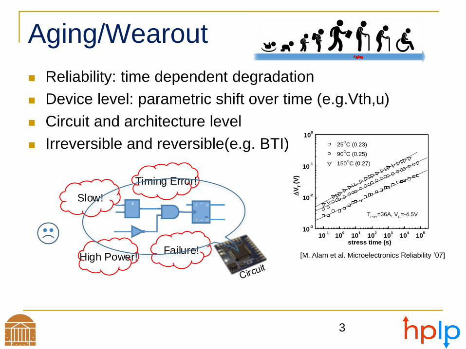
Aging/Wearout
Reliability: time dependent degradation
Device level: parametric shift over time (e.g.Vth,u)
Circuit and architecture level
Irreversible and reversible(e.g. BTI)
&0
0
0
Q
QSET
CLR
S
R
Timing Error!
High Power!Failure!
Slow!
10-1
100
101
102
103
104
105
10-3
10-2
10-1
100
TPHY
=36A, VG=-4.5V
25OC (0.23)
90OC (0.25)
150OC (0.27)
V
T (
V)
stress time (s)
[M. Alam et al. Microelectronics Reliability ’07]
3

Bias Temperature Instability(BTI)
Trapping/Detrapping [J. Velamala et al. DAC’12]
Get worse and worse
Both NBTI and PBTI
Stress and Recovery
4
[M. Lee et al. ASP-DAC ’11]
Time
∆Vth(t1)
t1 t1+t2
∆Vth
0
VstressRemove
VstressVstress
Remove
Vstress

Why Aging Sensor?
Track and monitor aging
Adaptive circuit tuning (e.g. DVFS)
“Check engine light” for recovery techniques
5

Related Work
Ring Oscillator based “Silicon Odometer”
[T. Kim et al. VLSI ’07, JSSC ’08]
- Area overhead, complex, process variation
Metastable element based
[A. Cabe et al. ISQED ’09][S. Wooters, et al. TVLSI ’12]
- Small and embedded
- Good time resolution
- Distributed
6

Sensor Cell
7Source: S. Wooters, et al. TVLSI ’12
Set the margin
Design the sensor
Check the engine

Why Top-Down Design?
Top-down design for sensor itself
- Reduce design time
- Reduce impact of process variations
- Designware cell
Top-down design with sensor embedded
- Different behavior of each block
- Different Thermal Behavior
- Distributed with Smaller area overhead
8

Sensor Cell Instantiate the library cell
9

Scan chain cell – Read Output
10
MUX
FFD
Scan_in
SE
clk
Q
Q
rst
Scan cell
New Scan Cell
MUX
FFD
Scan_in
SE
clk
Q
Q
rst
MUX
Aging Sensor
sel

Scan chain cell
11

agingsensor.v
Design Compiler
agingsensor_dc.vScancell
newscancell.v
Design Compiler
newscancell_dc.v
IC Compiler
agingsensor.CEL
agingsensor.FRAMIC Compiler
newscancell.CEL
newscancell.FRAM 12
New ScanCell Flow
Std cell lib

Architectural choices, RTL compilation and simulation(VCS)
Logic synthesis (Design Compiler)
Formal verification (Formality)
Generation of test patterns (TetraMAX)
Physical design (IC Compiler)
Physical Verification (Hercules)
Layout Parasitics Extraction (StarRC)
SPICE-level simulation of completed design (HSPICE)
Basic DC Synthesis(Design Compiler)
Basic Scan Synthesis Flow
(Design For Test Compiler)
Update the netlist
Add to Reference Library
(New scan cell library)
13
Top-down design with aging sensor embedded

Case Study: Johnson Counter
14
…
n=total # of SDFF;
t=user defined parameter; # application
dependent
for(i=0;i<=n;i+t)
{Replace the SDFFARX1 with sensorSDFFX1;
Add global control signals;
D=deg_in;
}
…
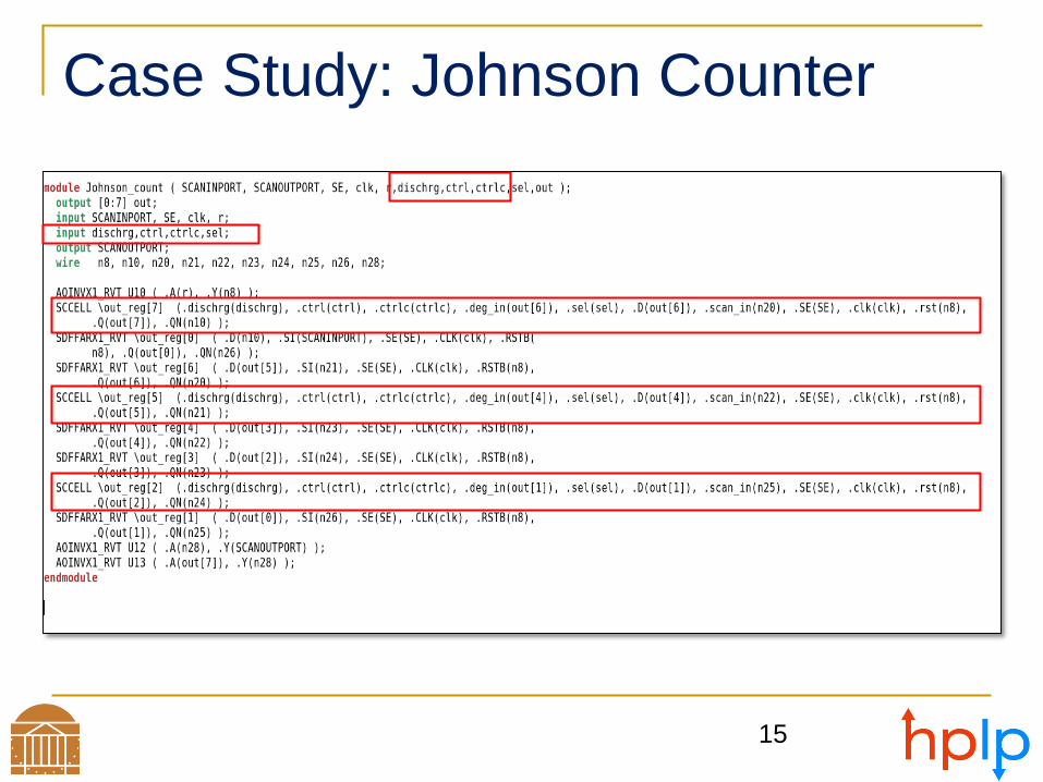
Case Study: Johnson Counter
15

Case Study: Johnson Counter
16
t=2
t=1

Future work
Verification
Tradeoff between # of sensor vs. accuracy
Placement of the sensor
Both NBTI and PBTI
Optimize area
Trigger recovery
Silicon Validation
17

Thanks!
Q & A
18


![100cm by 100cm Poster Template - people.Virginia.EDUpeople.virginia.edu/~xg2dt/papers/DAC PhD Forum Poster_Xinfei_Mircea.pdf · [2] X. Guo, M. Stan, “Letthe system sleep before](https://static.fdocuments.us/doc/165x107/5d20aceb88c9936a7a8db1ac/100cm-by-100cm-poster-template-xg2dtpapersdac-phd-forum-posterxinfeimirceapdf.jpg)