A Three-terminal Non-Volatile Ferroelectric Switch with an ...
23
1 A Three-terminal Non-Volatile Ferroelectric Switch with an Insulator- Metal Transition Channel Jaykumar Vaidya 1,a) , R S Surya Kanthi 1,a) , Shamiul Alam 2 , Nazmul Amin 2 , Ahmedullah Aziz 2 , Nikhil Shukla 1 * 1 Department of Electrical and Computer Engineering, University of Virginia, Charlottesville, VA- 22904, USA 2 Department of Electrical Engineering and Computer Science, University of Tennessee, Knoxville, TN 37996, USA a) equal contribution *e-mail: [email protected]
Transcript of A Three-terminal Non-Volatile Ferroelectric Switch with an ...

1
A Three-terminal Non-Volatile Ferroelectric Switch with an Insulator-
Metal Transition Channel
Jaykumar Vaidya1,a), R S Surya Kanthi1,a), Shamiul Alam2, Nazmul Amin2, Ahmedullah
Aziz2, Nikhil Shukla1*
1Department of Electrical and Computer Engineering, University of Virginia,
Charlottesville, VA- 22904, USA
2Department of Electrical Engineering and Computer Science, University of Tennessee,
Knoxville, TN 37996, USA
a) equal contribution
*e-mail: [email protected]
2
Abstract
Ferroelectrics offer a promising materials platform to realize energy-efficient non-
volatile memory technology with the FeFET-based implementations being one of
the most area-efficient ferroelectric memory architectures. However, the FeFET
operation entails a fundamental trade-off between the read and the program
operations. To overcome this trade-off, we propose in this work, a novel device,
Mott-FeFET, that aims to replace the Silicon channel of the FeFET with VO2- a
material that exhibits an electrically driven insulator-metal phase transition. The
Mott-FeFET design, which demonstrates a (ferroelectric) polarization-dependent
threshold voltage, enables the read current distinguishability (i.e., the ratio of
current sensed when the Mott-FeFET is in state 1 and 0, respectively) to be
independent of the program voltage. This enables the device to be programmed at
low voltages without affecting the ability to sense/read the state of the device. Our
work provides a pathway to realize low-voltage and energy-efficient non-volatile
memory solutions.

3
The electric-field (E-field) induced non-volatile polarization switching in ferroelectrics makes them
a promising candidate for developing non-volatile memory (NVM) technology. Conventionally,
ferroelectric-based random-access memory (RAM) was realized using traditional ferroelectrics
such as PZT, and showed energy-efficient operation, fast read as well as high endurance1,2.
However, this ferroelectric memory technology was challenging to scale since ferroelectrics such
as PZT exhibit a significant degradation in the ferroelectric response when the film thickness is
scaled below 50nm3 . Consequently, the recent discovery of ferroelectricity in highly scaled HfO2-
a material that is compatible with CMOS process technology- has generated immense interest in
revisiting ferroelectric memory technology4,5. Particularly, the ability to integrate the ferroelectric
directly into the gate of a field effect transistor (FET) has motivated active investigation of 1T-
FeFET (1 Transistor-Ferroelectric Field Effect Transistor)-based non-volatile memory6. While the
1T-FeFET architecture facilitates the realization of a dense array, it entails a fundamental trade-
off between the programming and the read/sensing characteristics7–9. The objective of this work
is to propose a pathway to overcome this trade-off by replacing the Silicon channel by an alternate
channel material, VO2 (vanadium dioxide), that exhibits the phenomenon of electrically driven
insulator-to-metal transition (IMT).
A conventional FeFET involves a fundamental trade-off between the program voltage (write
operation), and the MW (memory window) along with the corresponding read current
distinguishability, expressed as Ibit_1/Ibit_0 (Ibit_1 and Ibit_0 are the sense currents measured
corresponding to bit 1 and 0, respectively). Increasing the memory window and the corresponding
Ibit_1/Ibit_0 requires the application of a significantly larger programming voltage. This is because in
the FeFET configuration, the ferroelectric typically operates on a minor loop (not saturation loop)
of the polarization vs. voltage characteristics and improving the MW entails increasing the
hysteresis by the application of a larger programming voltage. Moreover, these contending factors
can become even more critical while operating the cell in a memory array where the parasitic
4
currents from half-selected cells can further compromise the read distinguishability. Additionally,
the larger program voltage also results in extremely large electric-fields (in excess of 10 MV/cm)
across the interlayer (IL) between the ferroelectric and the Silicon channel which can adversely
impact the reliability and the endurance of the device8. These trade-offs have been quantitatively
analyzed in prior works7,9 including those by the authors8,10.
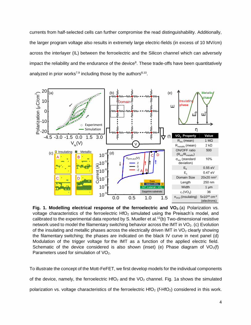
To illustrate the concept of the Mott-FeFET, we first develop models for the individual components
of the device, namely, the ferroelectric HfO2 and the VO2 channel. Fig. 1a shows the simulated
polarization vs. voltage characteristics of the ferroelectric HfO2 (f-HfO2) considered in this work.
Fig. 1. Modelling electrical response of the ferroelectric and VO2.(a) Polarization vs.
voltage characteristics of the ferroelectric HfO2 simulated using the Preisach’s model, and
calibrated to the experimental data reported by S. Mueller et al.12(b) Two-dimensional resistive
network used to model the filamentary switching behavior across the IMT in VO2. (c) Evolution
of the insulating and metallic phases across the electrically driven IMT in VO2 clearly showing
the filamentary switching; the phases are indicated on the black IV curve in next panel (d)
Modulation of the trigger voltage for the IMT as a function of the applied electric field.
Schematic of the device considered is also shown (inset) (e) Phase diagram of VO2(f)
Parameters used for simulation of VO2.
VO2 Property Value
Rins (mean) 1 MΩ
Rmetallic (mean) 2 kΩ
ON/OFF ratio
(Rins/Rmetallic)
500
σres (standard
deviation)
10%
Eb 0.55 eV
Ec 0.47 eV
Domain Size 20x20 nm2
Length 250 nm
Width 1 μm
(VO2) 36
nVO2 (insulating) 5x1018 cm-3
(electrons)
-4.5 -3.0 -1.5 0.0 1.5 3.0
-20
-10
0
10
20
Polarization
Po
lariza
tio
n (C
/cm
2)
Vfe(V)
(b)(a)
(f)
(e)
Domain
(c)A B
DC
Insulating Metallic
V
0.0 0.5 1.0 1.510
-9
10-8
10-7
10-6
10-5
10-4
Cu
rre
nt
(A)
Voltage(V)
Vgs = 0
Vgs = 2V
Vgs = -2V
BA
C D
2
0-2
VAPPLIED(V)
(d)
Cu
rre
nt (A
)
-4.5 -3.0 -1.5 0.0 1.5 3.0
-20
-10
0
10
20
Polarization
Po
larizatio
n
C/c
m2
Voltage(V)
ExperimentSimulation

5
These characteristics have been simulated using the phenomenological Preisach’s model11 and
have been calibrated to experimental data on 10nm thick f-HfO2 films (in a
metal/ferroelectric/metal capacitor configuration) reported by S. Mueller et al.12.
Next, we consider the electronically driven IMT in VO2. We note that while other oxides such as
NbO213, SmNiO3
14 among others also demonstrate similar electronically driven IMT behavior, VO2
was our choice of IMT material in this work since it exhibits a large ROFF/RON ratio (>104)15, and
more importantly, the modulation of the threshold voltage of the electrical IMT with gate electric
field, critical to the Mott-FeFET operation, has been experimentally demonstrated in this material
system16,17.
Two-terminal VO2 devices exhibit an electrically induced IMT that is characterized by an abrupt
change in resistance at a particular applied voltage (VT: threshold voltage) as the device
transitions from the insulating to the metallic state18. The transition is volatile, and the device
returns back to the insulating state (metal-to-insulator transition; MIT) when the applied voltage
subsequently drops below a threshold (VH: hold voltage), accompanied by hysteresis (VT-VH). To
simulate the electronically induced IMT in VO2, we model the two-terminal VO2 device as a
network of resistors that represent domains (Fig. 1b), as proposed in prior work19. Each resistance
in this 2D network can undergo an IMT and MIT (metal to insulator transition) with a certain
probability that is dependent on the voltage. Using the approach proposed by Madan et al.15 &
Poklonski et al.20, we model the switching probability for a domain using the following equations:
𝑃𝐼𝑀𝑇 = 𝑒−(𝐸𝑏 −
𝑞𝛥𝑉𝛾
)
𝑘𝑇 (1)
And,
PMIT = e−(Eb − Ec)
kT (2)

6
where PMIT and PIMT are the probabilities of a domain undergoing MIT and IMT, respectively; Eb
is the energy barrier between the insulating and the metallic state, γ is a geometric factor15, ψ𝑠 is
the VO2 surface potential due to the gate and α is the coupling constant introduced between the
gate-induced surface potential and the IMT transition in the VO2 device (set to 0.5). Eb and Ec are
defined in Fig. 1e.
It can be observed that applying a voltage increases the probability of a domain undergoing IMT.
Additionally, we also consider a gaussian distribution for the resistance values representing a
domain to account for the heterogeneity in the film. The parameters for the IMT in VO2 are shown
in the table in Fig. 1f. A detailed discussion of the electronic IMT in VO2 has been included in
supplement S3.
The voltage-induced IMT in the device can be explained as follows. Initially, all the domains are
in the insulating state (at zero bias). As the voltage across the device is increased, a few domains
(probabilistically) undergo IMT, serving as the nucleation centers for the metallic phase. As the
domain transitions to the metallic state, the voltage drop across the domain reduces, leading to a
corresponding increase in the voltage drop across other domains, which in turn, increases their
probability of switching. This process generates an avalanching effect that eventually creates a
metallic filamentary bridge between the electrodes, resulting in an abrupt change in resistance of
the device; the width of the filament on the current passing through the device- an effect that is
captured by our model as well (Fig. 1c). Furthermore, the presence of filamentary conduction has
been experimentally shown in prior work21. Similar (albeit weaker) avalanching behavior is
observed during MIT leading to an abrupt increase in resistance as the device turns OFF. We
also note that since the switching in VO2 is stochastic (see supplement S1a) which consequently
has important implications for the design of the memory array.
Additionally, in the three-terminal device configuration with a gate dielectric, Kim et al.16, and
Tabib-Azar et al.17 experimentally demonstrated that the threshold voltage of the VO2 channel can

7
be modulated by applying an electric field across the gate – a property crucial to the Mott-FeFET
operation. We note that the gate-field alone does not induce the IMT but aids the transition. We
model this behavior phenomenologically by modifying equation (1) to include the effect of surface
potential induced by the gate: 𝑃𝐼𝑀𝑇 = 𝑒−(𝐸𝑏 −
𝑞𝛥𝑉𝛾
− 𝛼𝑞𝜓𝑠)
𝑘𝑇 ; the surface potential of VO2 (which is
calculated using a capacitance divider analysis, similar to the gate stack in a standard FET) is
coupled to the probability of the IMT through a coupling constant α. Since the gate-field alone
does not induce the transition but modifies the threshold voltage (VT), we model this effect as the
surface potential modulating the probability of the domain switching, which subsequently,
manifests as the change in the (drain-to-source) VT required to induce the IMT, as shown in Fig.
1d. Additionally, we do not consider this effect in the MIT characteristics since the operation of
our proposed device as a memory cell does not rely on the MIT, as well as due to the absence of
experimental data. We also emphasize that while the proposed model can explain the
experimental behavior shown by Kim et al.16 and Tabib-Azar et al.17, it is important to qualify that
model is phenomenological in nature; the exact physics of the electrically induced Mott-Peierls
IMT in VO2 still remains an active, ongoing investigation.
Another important aspect of the gate electric-field induced modulation is that while it has a
significant influence on the threshold voltage for the IMT (by influencing the nucleation dynamics
of the metallic phase), its impact on the metallic and insulating states is minimal. This because
the high conductance state of the VO2 is essentially metallic in nature which limits the penetration
of the gate field. Furthermore, the impact of the electric field on the resistivity of insulating state
is also expected to be minimal22. This can be attributed to the formation of small polarons that
result from the gate-induced charge coupling to the lattice, as shown in our prior work23, as well
as in other works24. These polarons screen the electric field, and subsequently, limit its penetration
to a few (1-2) monolayers, resulting in minimal effect on the conductivity. This ensures that for a
current sensing-based reading scheme, the read distinguishability i.e., Ibit_1/ Ibit_0 would essentially

8
be constant, irrespective of the programming voltage / field applied at the gate. This behavior is
fundamentally different from that of a conventional Si transistor where the gate field strongly
controls the channel resistance, and consequently, the channel current.
The Mott-FeFET design (Fig. 2a) aims to integrate the non-volatile polarization switching in the
ferroelectric gate with the abrupt resistance switching across the electrically driven IMT in VO2
channel. The expected operation of the Mott-FeFET can be described as follows: the polarization
state (up or down) of the ferroelectric gate is used to represent the information bit to be stored
and can be programmed (write operation) by applying the program voltage across the gate of the
device (details of the polarity are discussed in the array operation). The resulting surface potential
associated with the (different) polarization states of the ferroelectric modulates the threshold
voltage (VT,1, VT,0) of the IMT in the VO2 channel i.e., one polarization state results in a larger
threshold voltage than the other state, creating a memory window (ΔVT = VT,0 - VT,1) as shown in
Fig. 2b. Subsequently, the state of the memory can be sensed by applying an appropriate read
voltage VREAD such that VT,1 < VREAD < VT,0. This ensures that if the memory cell is in state 1, a
large drain current, corresponding to the metallic state of VO2, will be sensed whereas state 0 will
produce a significantly smaller drain current owing to the insulating nature of the channel.
Fig. 2. Mott-FeFET operation. (a) Schematic of the proposed Mott-FeFET. (b) Ids vs. Vds characteristics of the VO2 channel as a function of the ferroelectric polarization. (c) Observed ratio between read currents corresponding to state 1 and 0, as a function of the applied program voltage. It can be observed that ION/IOFF ratio, unlike in a conventional FeFET remains constant.
VDS (V)
0.0 0.5 1.0 1.5
10-8
10-7
10-6
10-5
10-4
10-3
Y A
xis
Title
X Axis Title
B
2.0 2.5 3.0 3.5 4.0
0
200
400
600
On-Off ratio
Y A
xis
Title
Read voltage(V)
2.0 2.5 3.0 3.5 4.0
0.2
0.4
0.6
0.8
MW
Y A
xis
Title
Read voltage(V)
VR
EA
D
(b)
Vprog. (V)
2.0 2.5 3.0 3.5 4.0
0
250
500
On-Off ratio
Y A
xis
Title
Read voltage(V)
2.0 2.5 3.0 3.5 4.0
0.2
0.4
0.6
Memory window
Read voltage(V)
On/Off ratio
MW
MW
(V)I O
N/I
OF
F
(c)
+P( )
-P( )
I DS
(A
)
Sapphire substrate
IMT material – VO2
Fe-HZO +P -P
Gate
DS
(a)
Interlayer
MW

9
Therefore, the VO2 channel can be considered as a ‘selector’ whose threshold voltage depends
on the state of the memory (i.e., ferroelectric gate).
We explore the operation of the proposed Mott-FeFET by integrating the models developed above
for the individual components, namely, polarization switching in the ferroelectric and the
electronically induced abrupt resistance switching in VO2. Moreover, the ferroelectric polarization
interacts with the VO2 channel through the surface potential which is calculated by modeling the
capacitance response of the gate stack. The surface potential, which depends on the state of
polarization of the ferroelectric, subsequently, modulates the probability of the switching (from
insulating to metallic state) in the VO2 domains, resulting in a ferroelectric polarization state
dependent IMT threshold voltage. A finite interlayer at the interface between the ferroelectric and
the VO2 is also considered. Using this framework, we simulate the characteristics of the Mott-
FeFET, as shown in Fig. 2b. It can be observed that the threshold voltage for the IMT in the VO2
channel varies by ~0.5V, opening a memory window that can facilitate its use a non-volatile
storage element.
We note that while the memory window (i.e., ΔVT = VT,0 - VT,1) is sensitive to the polarization, which
in turn depends on the voltage used to program the ferroelectric, the Ibit_1/ Ibit_0 ratio (within the
memory window) is almost insensitive to the program voltage of the ferroelectric, as observed in
Fig. 2c. This is because the current distinguishability is primarily decided by the ROFF and RON of
the VO2 which are insensitive to the gate-field, as discussed above. The insensitivity of the Ibit_1/
Ibit_0 ratio to the program voltage can facilitate scaling of the program voltage without adversely
impacting the read/sense characteristics and margins.

10
Next, we evaluate the operation of the Mott-FeFET as a memory element in a non-volatile memory
array. We consider the NOR memory architecture as shown in Fig. 3a, where the basic building
Figure 3. Mott-FeFET array operation. (a) Schematic of the proposed Mott-FeFET-based memory array. (b) Biasing scheme for WLWs, WLRs, BLs and SLs to access a memory cell (M22 here). The results presented here are for a 3×3 array. Time dynamics of the bias voltages applied across WLW2 and BL2 during (c) write ‘0’ and (d) write ‘1’ operations in the M22 cell. During write operation, the other WLWs and BLs are biased at VDD and 0 V, respectively, and all the WLRs and SLs are biased at 0 V. Time evolution of the ferroelectric polarization for (e) write ‘1’ → ’0’ and (f) write ‘0’ → ’1’ operations in the M22 cell. (g) Temporal dynamics of the bias voltages of WLW2 and WLR2 for read operation of the cells in the second row. The bias voltages for other WLWs, WLRs, BLs and SLs are kept constant at specific levels (shown in (b)). (h) SL currents during read operation. This array architecture facilitates reading the entire row in one cycle. Here, we only read the second row. M21 and M23 cells were initialized with logic ‘0’ and M22 with logic ‘1’ before read operation. The effect of the stored memory state is observed in the corresponding SL currents. SL1 and SL3 currents are 450 nA due to logic ‘0’ in M21 and M23 and SL2 current is 225 µA due to logic ‘1’ stored in M22.
WLR1
BL1 SL1
WLW1
WLR2
WLW2
WLRm
WLWm
SL2SLnBL2 BLn
M11 M12 M1n
M21 M22 M2n
Mm1 Mm2 Mmn
ISL1 ISL2 ISLn
VW
LW
2(V
)
0
1
2
3
4
0
-1
-2
-3
-4
VB
L2
(V)
2
4
0
-2
-4
-6
-8
0 5 10 15 20 25 30
Time (ns)
VW
LW
2(V
)
0
1
2
3
4
0
1
2
3
4
VB
L2
(V)
0 5 10 15 20 25 30
Time (ns)
8
10
6
4
2
0
Po
lariza
tio
n (
µC
/cm
2)
Po
lariza
tio
n (
µC
/cm
2)
(a) (b)
(c) (d)
(e) (f)
VW
LW
2(V
)
0
1
2
3
4
0
0.9
VW
LR
2(V
)
0 5 10 15 20 25 30
Time (ns)
0
0.45
25
0
50
0
150
300
0
I SL (µ
A)
I SL (n
A)
(g)
(h)
Write ‘0’ Operation in M22 Cell Write ‘1’ Operation in M22 Cell Read Operation in 2nd Row
Logic ‘0’
Logic ‘1’
Logic ‘0’
Logic ‘1’
-2
ISL1ISL2
ISL3

11
block of the array consists of the Mott-FeFET as the memory element whose gate is connected
to a simple MOSFET, which functions as the access device. This architecture, which consists of
a separate word-line to read (WLR) from, and write (WLW) to, a cell is similar to that proposed for
FeFET-based memory arrays25. A phenomenological Verilog-A model is used to simulate the
Mott-FeFET whereas the DGXFET NMOS model, available in the IBM 65nm CMOS 10LPe
process, is used for the transistor.
The biasing scheme for reading from-, and writing to-, a particular cell of the memory array is
designed to facilitate successful reading and writing operations, without disturbing other cells in
the array. Here, we consider the illustrative example of accessing the M22 cell in a 3x3 array. The
corresponding biasing conditions are shown in Fig. 3b. Figures 3c,d show the bias voltages
applied to WLW2 and BL2 (connected with M22) for the write ‘0’ and write ‘1’ operations,
respectively. The bias conditions for the other WLWs, BLs, WLRs, and SLs are in accordance
with those listed in the table in Fig. 3b. The WLW2 is asserted to turn ON the access transistors
of the second row, and a suitable programming voltage (±VWRITE) is applied to the BL2 with the
objective to facilitate sufficient bias at the gate of the Fe to modulate the polarization, as needed.
Figures 3e,f show the evolution of the ferroelectric polarization during write ‘1’ → ‘0’ and write ‘0’
→ ‘1’ operations, respectively. The choice of the suitable bias conditions eliminates the possibility
of the accidental write into the other cells of the array (details discussed in supplement S4).
The proposed array architecture also facilitates reading all the cells in a row in one cycle. To
illustrate this, we initially store ‘0’ in M21 and M23 and ‘1’ in M22 cells belonging to the second row
of the 3 x 3 array. To read from a cell, we utilize the IDS-VDS characteristics of Mott-FeFET (at zero
gate bias) shown in Fig. 2b. Figure 3g shows the bias conditions for the WLW2 and WLR2 and the
corresponding SL currents are shown in Fig. 3h. It can be observed that the SL connected to the
cell with logic ‘0’ generates ~450 nA whereas the logic 1 produces a current of ~225 µA on SL.

12
This difference in the SL current is used for the sensing of the stored memory states using current
sense amplifiers26,27 (see supplement S4 for more details on the sensing mechanism).
Discussion
The goal of this work is to propose and elucidate a new device concept, Mott-FeFET, that aims
to overcome the read-write trade-offs in conventional Silicon FeFET designs by leveraging the
unique properties of IMT. It showcases an example of how novel functional materials and their
properties (here, the IMT in VO2) can be used to overcome the design challenges of Silicon
devices. While the focus of the work is primarily to describe the operational characteristics and
functional properties of the Mott-FeFET, it is important to note that the physical realization of such
a device would inevitably need to address important challenges such as the integration of the f-
HfO2 on VO2 while retaining their functional properties, the role of the interfacial layer and interface
states among others; overcoming these concerns will be critical to the eventual practicality of such
a device. Additionally, we also note that the underlying physics of the electrically induced IMT in
VO2 as well as how an external electric field affects the IMT still remain to be fully understood.
However, the present work helps nucleate the new device concept, and motivates the
investigation of the above questions, which can subsequently, enable energy-efficient and high
performance non-volatile random-access memory.
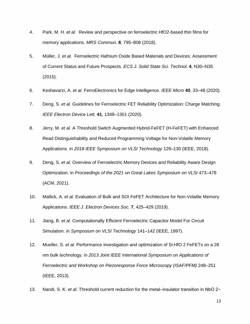
References
1. Kato, Y. et al. Overview and Future Challenge of Ferroelectric Random Access Memory
Technologies. Jpn. J. Appl. Phys. 46, 2157–2163 (2007).
2. Arimoto, Y. et al. Current Status of Ferroelectric Random-Access Memory. MRS Bull. 29,
823–828 (2004).
3. Zambrano, R. Challenges for Integration of Embedded FeRAMs in the sub-180 nm
Regime. Integr. Ferroelectr. 53, 247–255 (2003).
13
4. Park, M. H. et al. Review and perspective on ferroelectric HfO2-based thin films for
memory applications. MRS Commun. 8, 795–808 (2018).
5. Müller, J. et al. Ferroelectric Hafnium Oxide Based Materials and Devices: Assessment
of Current Status and Future Prospects. ECS J. Solid State Sci. Technol. 4, N30–N35
(2015).
6. Keshavarzi, A. et al. FerroElectronics for Edge Intelligence. IEEE Micro 40, 33–48 (2020).
7. Deng, S. et al. Guidelines for Ferroelectric FET Reliability Optimization: Charge Matching.
IEEE Electron Device Lett. 41, 1348–1351 (2020).
8. Jerry, M. et al. A Threshold Switch Augmented Hybrid-FeFET (H-FeFET) with Enhanced
Read Distinguishability and Reduced Programming Voltage for Non-Volatile Memory
Applications. in 2018 IEEE Symposium on VLSI Technology 129–130 (IEEE, 2018).
9. Deng, S. et al. Overview of Ferroelectric Memory Devices and Reliability Aware Design
Optimization. in Proceedings of the 2021 on Great Lakes Symposium on VLSI 473–478
(ACM, 2021).
10. Mallick, A. et al. Evaluation of Bulk and SOI FeFET Architecture for Non-Volatile Memory
Applications. IEEE J. Electron Devices Soc. 7, 425–429 (2019).
11. Jiang, B. et al. Computationally Efficient Ferroelectric Capacitor Model For Circuit
Simulation. in Symposium on VLSI Technology 141–142 (IEEE, 1997).
12. Mueller, S. et al. Performance investigation and optimization of Si:HfO 2 FeFETs on a 28
nm bulk technology. in 2013 Joint IEEE International Symposium on Applications of
Ferroelectric and Workshop on Piezoresponse Force Microscopy (ISAF/PFM) 248–251
(IEEE, 2013).
13. Nandi, S. K. et al. Threshold current reduction for the metal–insulator transition in NbO 2−

14
x -selector devices: the effect of ReRAM integration. J. Phys. D. Appl. Phys. 48, 195105
(2015).
14. Shukla, N. et al. Electrically induced insulator to metal transition in epitaxial SmNiO 3 thin
films. Appl. Phys. Lett. 105, 012108 (2014).
15. Madan, H. et al. Quantitative Mapping of Phase Coexistence in Mott-Peierls Insulator
during Electronic and Thermally Driven Phase Transition. ACS Nano 9, 2009–2017
(2015).
16. Kim, H.-T. et al. Mechanism and observation of Mott transition in VO2 -based two- and
three-terminal devices. New J. Phys. 6, 52–52 (2004).
17. Tabib-Azar, M. et al. Nano-Particle VO2 Insulator-Metal Transition Field-Effect Switch with
42 mV/decade Sub-Threshold Slope. Electronics 8, 151 (2019).
18. Shukla, N. et al. Synchronized charge oscillations in correlated electron systems. Sci.
Rep. 4, 4964 (2015).
19. Driscoll, T. et al. Current oscillations in vanadium dioxide: Evidence for electrically
triggered percolation avalanches. Phys. Rev. B 86, 094203 (2012).
20. Poklonski, N. A. et al. Simulation of dc conductance of two-dimensional heterogeneous
system: application to carbon wires made by ion irradiation on polycrystalline diamond.
Phys. status solidi 243, 1212–1218 (2006).
21. Freeman, E. et al. Nanoscale structural evolution of electrically driven insulator to metal
transition in vanadium dioxide. Appl. Phys. Lett. 103, 263109 (2013).
22. Sengupta, S. et al. Field-effect modulation of conductance in VO2 nanobeam transistors
with HfO2 as the gate dielectric. Appl. Phys. Lett. 99, 062114 (2011).

15
23. Martens, K. et al. Field Effect and Strongly Localized Carriers in the Metal-Insulator
Transition Material VO 2. Phys. Rev. Lett. 115, 196401 (2015).
24. Yajima, T. et al. Modulation of VO2 Metal–Insulator Transition by Ferroelectric HfO2 Gate
Insulator. Adv. Electron. Mater. 6, 1901356 (2020).
25. George, S. et al. Nonvolatile memory design based on ferroelectric FETs. in Proceedings
of the 53rd Annual Design Automation Conference 1–6 (ACM, 2016).
26. Chang, M.-F. et al. An Offset-Tolerant Fast-Random-Read Current-Sampling-Based
Sense Amplifier for Small-Cell-Current Nonvolatile Memory. IEEE J. Solid-State Circuits
48, 864–877 (2013).
27. Aziz, A. et al. Low power current sense amplifier based on phase transition material. in
2017 75th Annual Device Research Conference (DRC) 1–2 (IEEE, 2017).
Acknowledgments
This work was supported by NSF grant 1914730.
Author contributions
J.V., R.S.S.K. performed the device simulations. S.A. and N.A performed the array
simulations. J.V. and N.S. conceived the idea. A.A. and N. S. supervised the study. All

16
authors took part in writing the manuscript, discussed the results and commented on the
manuscript.
Competing interests
The authors declare no competing interests.
Additional information
Correspondence should be addressed to N. S.

17
Supplementary Information
A Three-terminal Non-Volatile Ferroelectric Switch with an Insulator-
Metal Transition Channel
Jaykumar Vaidya1,a), R S Surya Kanthi1,a), Shamiul Alam2, Nazmul Amin2, Ahmedullah
Aziz2, Nikhil Shukla1*
1Department of Electrical and Computer Engineering, University of Virginia,
Charlottesville, VA- 22904, USA
2Department of Electrical Engineering and Computer Science, University of Tennessee,
Knoxville, TN 37996, USA
a) equal contribution
*e-mail: [email protected]

18
S1. Stochastic switching in VO2
Fig. S1. Stochastic nature of switching in VO2. (a) Distribution of IMT threshold voltage in 2 terminal
VO2 device (25 sweeps were considered). (b) Distribution of threshold voltages corresponding to the
two states of the ferroelectric in the Mott-FeFET (25 sweeps were simulated).
Threshold voltage (V)
Co
un
t
IMT 1
(P )
IMT 2
(P )
Threshold voltage (V)
(a) (b)
IMT
Without ferroelectric

19
S2. Electrically driven IMT in VO2 (Experimental characteristics)
Illustrative I-V characteristics showing electrically induced IMT and MIT in VO2 marked by an
abrupt and hysteretic change in resistance. The device length and width was 10 µm.
Fig. S2. Current vs. voltage characteristics of VO2. Illustrative current vs. voltage characteristics of
VO2 measured experimentally in a two-terminal device configuration shown using a (a) Linear scale,
(b) Logarithmic scale for the current axis.
-3 0 3
1
10
100
C
-3 0 3
-100
-50
0
50
100
VVO2 (V)
I VO
2(m
A)
T = 300 K
VVO2 (V)
I VO
2(m
A)
(a) (b)

20
S3. Nature of the electrical IMT in VO2
The origin of the IMT in VO2 has been the subject of intense research and debate1. Various
models based on varying levels of contribution from a Mott-Hubbard type transition and a Peierls-
like structural instability have been proposed to explain the transition. However, a comprehensive
understanding of the exact origins of the IMT in VO2 still remains elusive. Consequently, this also
implies that the exact mechanism of how an external stimulus such as an electric field affects the
IMT in VO2 also remains to be completely understood.
Electronically driven IMT in VO2: Two-terminal VO2 devices exhibit an IMT when a voltage is
applied across the VO2 channel. In this configuration, both electric-field and current-induced Joule
heating effects are present2. While the exact origin of this transition is also disputed, there is
increasing evidence of the preponderance of electro-thermal effects3,4. In a three-terminal device,
a true gate-field induced IMT has not been demonstrated, although several useful features of the
interaction between the (gate) electric-field and the VO2 channel have been revealed (we note
that Nakano et al5. demonstrated a non-volatile phase transition using ionic liquid gating where
the role of ionic diffusion and the electric field are challenging to deconvolute). A key feature of
the application of an electric field (through the gate) on the VO2 channel is that it modulates the
(threshold) voltage required at the source-drain to induce IMT6 - a property that facilitates the
design of the Mott FeFET proposed here. One possible explanation for this behavior is that even
though the magnitude of the electric-field required to induce an IMT is significantly larger than that
which can supported by a solid state dielectric, the field modulates the nucleation probability of
the metallic phase (field induced nucleation) resulting in the change in the threshold voltage. We
therefore propose a phenomenological model to emulate this behavior.
Fig. S3 Variation in IMT threshold voltage as a function of the applied gate voltage as reported by
Tabib-Azar et al 3.
-4 -2 0 2 4
0.0
0.2
0.4
Change in threshold voltage
V
IMT
(V)
Gate voltage(V)
21
S4. Design and operation of Mott-FeFET array
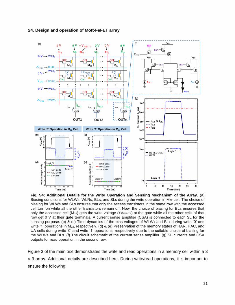
Figure 3 of the main text demonstrates the write and read operations in a memory cell within a 3
× 3 array. Additional details are described here. During write/read operations, it is important to
ensure the following:
Fig. S4: Additional Details for the Write Operation and Sensing Mechanism of the Array. (a) Biasing conditions for WLWs, WLRs, BLs, and SLs during the write operation in M22 cell. The choice of biasing for WLWs and SLs ensures that only the access transistors in the same row with the accessed cell turn on while all the other transistors remain off. Now, the choice of biasing for BLs ensures that only the accessed cell (M22) gets the write voltage (±VWRITE) at the gate while all the other cells of that row get 0 V at their gate terminals. A current sense amplifier (CSA) is connected to each SL for the sensing purpose. (b) & (c) Time dynamics of the bias voltages of WLW2 and BL2 during write ‘0’ and write ‘1’ operations in M22, respectively. (d) & (e) Preservation of the memory states of HAR, HAC, and UA cells during write ‘0’ and write ‘1’ operations, respectively due to the suitable choice of biasing for the WLWs and BLs. (f) The circuit schematic of the current sense amplifier. (g) SL currents and CSA outputs for read operation in the second row.
VW
LW
2(V
)P
ola
riza
tio
n (
C/c
m2)
Time (ns)
Logic ‘1’
01234
0-1
-2
-3
-4
VB
L2
(V)
Logic ‘1’HAR Cells
HAC Cells
UA Cells
Po
lari
za
tio
n (
C/c
m2)
Time (ns)
Logic ‘0’ Logic ‘0’
HAR Cells
HAC Cells
UA Cells
(b) (c)
(d) (e)
(a)
Write ‘0’ Operation in M22 Cell Write ‘1’ Operation in M22 Cell
VW
LW
2(V
)
01
2
3
4
01234
VB
L2
(V)
OFF OFF OFF
OFF OFF OFF
0 V VWRITE 0 V
ON ON ON
OUT1
CSA CSA CSA
OUT2 OUTn
ISL1 ISL2 ISLnIREF IREF IREF
(g)
(f)
Time (ns)
SL
Cu
rre
nt,
IS
L (A
)

22
(i) The stored data in the inactive cells does not get disturbed during the read/write operations
(ii) During the read operation, the SL current shows distinguishable difference for low/high
memory states
We first discuss the possibility of the accidental manipulation of the data stored in the inactive
cells. Note, in the Mott-FeFET based memory cells, the write and the read operations are
performed using the gate and drain bias, respectively. For write (read) operation, suitable VWRITE
(VREAD) is applied as VGS (VDS), while VDS (VGS) is kept at 0 V. Thus, accidental programming in
the inactive cells can be avoided while reading from the active cells. Now, during the write
operation, the biasing conditions for the WLWs, WLRs, BLs and SLs (shown in Fig. S4a) are
carefully chosen to ensure that, only the accessed cell gets the programming voltage at the gate
terminal. The biasing of WLWs (Fig. S4b,c) ensures that the access transistors of half-accessed
column (HAC) and unaccessed (UA) cells remain off7. Although the access transistors of half-
accessed row (HAR) cells turn ON, the BL biasing (Fig. S4b,c) ensures that the HAR cells get 0
V at their gate terminals. Therefore, the memory states of the HAR, HAC, UA cells remain
undisturbed during both the write ‘0’ (Fig. S4d), and the write ‘1’ (Fig. S4e) operations.
Next, we discuss the distinguishability in the SL currents during the read operation. We utilize the
difference in the SL currents to sense the memory states stored in the cells of an array. Fig. 4h in
the main text shows the SL currents for the read operation of the memory cells in the second row.
It clearly shows that the SL currents provide sufficient distinguishability between logic ‘0’ and logic
‘1’ states. For sensing, a current sense amplifier (CSA) is connected to each SL, as shown in Fig.
S4a. Figure S4b shows the schematic of the CSA8 that we have used in this work. The reference
current (IREF= 10 A) is appropriately chosen to obtain different binary outputs (0 and VDD) for logic
‘0’ and logic ‘1’, respectively. Figure S4c shows the SL currents and corresponding logic outputs
of the CSA during the read operation.

23
References
1. Shao, Z., Cao, X., Luo, H. & Jin, P. Recent progress in the phase-transition mechanism
and modulation of vanadium dioxide materials. NPG Asia Mater. 10, 581–605 (2018).
2. Farjadian, M. & Shalchian, M. Hybrid Electrothermal Model for Insulator-to- Metal
Transition in VO2 Thin Films. IEEE Trans. Electron Devices 68, 704–712 (2021).
3. Tabib-Azar, M. & Likhite, R. Nano-Particle VO2 Insulator-Metal Transition Field-Effect
Switch with 42 mV/decade Sub-Threshold Slope. Electronics 8, 151 (2019).
4. P, A., Chauhan, Y. S. & Verma, A. Vanadium dioxide thin films synthesized using low
thermal budget atmospheric oxidation. Thin Solid Films 706, 138003 (2020).
5. Nakano, M. et al. Collective bulk carrier delocalization driven by electrostatic surface
charge accumulation. Nature 487, 459–462 (2012).
6. Kim, H.-T. et al. Mechanism and observation of Mott transition in VO2 -based two- and
three-terminal devices. New J. Phys. 6, 52–52 (2004).
7. Aziz, A., Jao, N., Datta, S., Narayanan, V. & Gupta, S. K. A computationally efficient
compact model for leakage in cross-point array. in 2017 International Conference on Simulation
of Semiconductor Processes and Devices (SISPAD) 141–144 (IEEE, 2017).
doi:10.23919/SISPAD.2017.8085284.
8. Chang, M.-F. et al. An offset-tolerant current-sampling-based sense amplifier for Sub-
100nA-cell-current nonvolatile memory. in 2011 IEEE International Solid-State Circuits
Conference 206–208 (IEEE, 2011). doi:10.1109/ISSCC.2011.5746284.


![FERROELECTRIC RAM [FRAM]](https://static.fdocuments.us/doc/165x107/56816799550346895ddcd567/ferroelectric-ram-fram.jpg)


![Sangeetha [Ferroelectric Memory]](https://static.fdocuments.us/doc/165x107/55cf8f91550346703b9d9665/sangeetha-ferroelectric-memory.jpg)