A Thesis Presented for the Master of Science Degree The ...
63
AN EVALUATION OF LOW COST FPGA-BASED SOFTWARE DEFINED RADIOS FOR EDUCATION AND RESEARCH A Thesis Presented for the Master of Science Degree The University of Tennessee at Chattanooga Abhilash M. Purani April 23, 2010
Transcript of A Thesis Presented for the Master of Science Degree The ...

AN EVALUATION OF LOW COST FPGA-BASED SOFTWARE DEFINED RADIOS
FOR EDUCATION AND RESEARCH
A Thesis
Presented for the
Master of Science Degree
The University of Tennessee at Chattanooga
Abhilash M. Purani
April 23, 2010

ii
To the Graduate Council:
I am submitting herewith a thesis written by Abhilash M. Purani entitled “An Evaluation
of Low Cost FPGA-Based Software Defined Radios for Education and Research.” I have
examined the final electronic copy of this thesis for form and content and recommend
that it be accepted in partial fulfillment of the requirements for the degree of Master of
Science, with a major in Electrical Engineering.
Dr. Stephen Craven Major advisor We have read this thesis And recommend its acceptance: Dr. Ahmed Eltom Dr. Clifford Parten Accepted for the Council: Dr. Stephanie Bellar Interim Dean of the Graduate School

iii
ABSTRACT
The purpose of this study is to evaluate a low-cost Software Defined Radio (SDR)
platform for educational and research purposes. An evaluation of existing SDR platforms
and design techniques was performed, identifying low cost hardware and software
suitable for a laboratory environment. The idea behind the project is to provide
undergraduate students with a generic hardware platform so that they can perform simple
radio communication experiments.
This paper compares and evaluates the existing research projects and educational
lab experiments done for SDR. Basic AM and FM radios are created and simulated on the
hardware. The detailed procedure to create a design and download the design onto the
hardware has been documented, and tutorials are created for step-by-step procedures to
perform the experiments. With their ease of use and low cost, Spartan3E FPGA board
and Simulink are the best choices for conducting low frequency radio communication
experiments.

iv
ACKNOWLEDGEMENT
First and foremost I would like to offer my sincere gratitude to my advisor Dr.
Stephen Craven, who guided me and encouraged me throughout this thesis. He has been a
very friendly advisor and a constant source of inspiration. He was always accessible and
willing to help, and without whom this thesis would not have been possible.
I would also like to thank Dr. Ahmed Eltom and Dr. Clifford Parton for their
interest in the project and for being a part of my committee. I thank the Department of
Electrical Engineering at University of Tennessee at Chattanooga for providing me with
the lab, and all the necessary equipments required for this project.
I would also like to thank all the lab-mates for making the lab a vey congenial
environment to work in, and their helping hand towards my thesis.
Finally, I would like to thank my parents, my family members and all my friends
for believing in me and motivating me throughout this journey.

v
TABLE OF CONTENTS
CHAPTER PAGE
I. Abstract iii
II. Acknowledgement iv
III. List of figures vi
IV. List of tables vii
V. List of abbreviations viii
1. Introduction 1
2. Background 4
3. Design entry methods 14
4. Hardware platform comparison 27
5. Lab experiments and results 34
6. Conclusion 40
Bibliography 41
Appendix A.1 MATLAB code for AM modulation 45
Appendix A.2 AccelDSP code for AM modulation in MATLAB 47
Appendix A.3 System Generator instructions 48

vi
LIST OF FIGURES
1. Figure 2.1 Basic block diagram of SDR 6
2. Figure 2.2 USRP classic board 9
3. Figure 2.3 TIMS at electrical communications laboratory at UTC 12
4. Figure 3.1 AccelDSP process flow 19
5. Figure 3.2 AM modulation AccelDSP script code 19
6. Figure 3.3 AM modulation AccelDSP function file 20
7. Figure 3.4 AccelDSP window with RTL report for AM modulation 22
8. Figure 3.5 AM radio using Simulink 23
9. Figure 3.6 FFT of input radio stations 24
10. Figure 3.7 Input plot (a) and Output plot (b) of AM demodulation
with Simulink 25
11. Figure 4.1 USRP with daughterboards 29
12. Figure 4.2 Spartan 3E Starter Board 30
13. Figure 5.1 AM modulation in System Generator 35
14. Figure 5.2 Modulating signal 36
15. Figure 5.3 Carrier signal 36
16. Figure 5.4 Modulated signal observed with System Generator 36
17. Figure 5.5 Modulated signal on oscilloscope 37
18. Figure 5.6 ASK modulation 38
19. Figure 5.7 ASK modulated signal 39

vii
LIST OF TABLES
1. Table 2.1 SDR projects comparison 13
2. Table 4.1 USRP versus Spartan 3E comparison 31
3. Table 4.2 SDR projects comparison 32

viii
LIST OF ABBREVIATIONS
ADC – Analog to Digital Converter
ASIC – Application Specific Integrated Circuit
ASK – Amplitude Shift Keying
DAC – Digital to Analog Converter
DSP – Digital Signal Processing
FPGA – Field Programmable Gate Array
GPL – General Public License
HDL – Hardware Description Language
HPSDR – High Performance Software Defined Radio
IF – Intermediate Frequency
MBD – Model Based Design
MIMO – Multi Input Multi Output
OSSIE - Open-Source Software Communications Architecture Implementation –
Embedded
PSoC – Programmable System on Chip
RF – Radio Frequency
RTL – Register Transfer Level

ix
SDR – Software Defined Radio
USRP – Universal Software Radio Peripheral
WARP – Wireless Open Access Research

1
Chapter 1
Introduction
Communication is a way of exchanging information between two entities. Since
the invention of radio, communication has expanded and the world has come closer.
Currently, radio communication has become an essential part of everyday life. Radio
communication exists around us in the form of television, radio receiver, cellular phones
and many such devices.
The term Software Defined Radio (SDR), as the name suggests, is a radio
communication technology in which the radio receiver is implemented using software, or
some similar reconfigurable medium, thus reducing the amount of hardware required.
Since an SDR can be programmed to adjust its own parameters, it can adapt to changing
conditions and standards.
This thesis discusses a low cost software defined radio using a Field
Programmable Gate Array (FPGA) board for educational purposes. The FPGA is an
integrated circuit which can be dynamically configured according to the design. It can be
programmed through a hardware description language (HDL) such as Verilog (VHDL).
An HDL is a language used to describe electronic and digital logic circuits. The Register
Transfer Level (RTL) concept is used in HDLs to create high-level representations of a
circuit, from which a lower-level representation can be derived. Because HDLs are
difficult to learn, use, and verify, high level design environments have been created that
enable the description and simulation of hardware such as MATLAB or Simulink.

2
The goal of the project is to define a generic platform using SDR technology so
that the students can build and simulate their own radios. This thesis discusses various
design entry methods used for creating SDRs and simulating them, avoiding HDLs while
leveraging skills that undergraduate engineering students already know.
Chapter 2 is a literature review. It discusses the background of the project and the
existing technologies in the SDR field. It discusses the workings of an SDR and its
various aspects. It also discusses the advantages and constraints of SDR. The subsequent
sections in the chapter discuss existing SDR projects used for educational and research
purpose and the available communication lab facilities at University of Tennessee at
Chattanooga (UTC).
Chapter 3 considers actual design and coding methods. It discusses various
design entry methods for SDR. It describes AM and FM radio designs which were
created and simulated on MATLAB as well as AccelDSP. The detailed description of
creating and simulating an AM radio in MATLAB and with AccelDSP is discussed in
detail in the subsequent sections. Chapter 4 presents hardware platform comparisons. It
compares the hardware selected for this project, the Xilinx Spartan 3E Starter Kit Board,
with most commonly used hardware for SDRs such as the USRP board. It describes the
features of both the mentioned boards. A comparison between the educational research
projects used in universities is also presented.
All the lab experiments and results are discussed in Chapter 5. Discussed there is
the AM radio and ASK modulation design created using System Generator and its
implementation in hardware. The simulation output is compared with the output taken

3
from FPGA board. Chapter 6 is the final chapter in which conclusions are made for this
thesis.

4
Chapter 2
Background
A Software Defined Radio (SDR) is a technology used for radio communication
which implements the components required for the radio system with software or
programmable hardware. As defined by the IEEE P1900.1 group, SDR can simply be
defined as a radio in which some or all of the physical layer functions are software
defined [1]. Joseph Mitola is quoted as saying, "A software radio is a radio whose
channel modulation waveforms are defined in software. That is, digital waveforms are
generated and converted to analog form using a Digital to Analog Converter (DAC) at the
transmitter and at the receiver, they are converted to digital form using Analog to Digital
Converter (ADC) and demodulated using the software" [5]. An SDR can be implemented
on a Digital Signal Processing (DSP) engine, such as General Purpose (GP)
microprocessors, Programmable System on Chip (PSoC), Application Specific Integrated
Circuits (ASICs), Field Programmable Gate Arrays (FPGAs), or specialized co-
processors.
SDR technology was proposed in the early 1990s by Joseph Mitola [5]. It was
initially used for military radio systems. The main purpose for implementing this
technology was to incorporate multiple radio channels within a specified frequency
bandwidth. Since the early 1990s, there has been much advancement in SDR. Now, SDR
supports analog as well as digital radios and their respective communication standards
and protocols.
Currently, a radio exists in almost all electronic devices which are used for
communication, such as cell phones, televisions, computers and vehicles. When it comes
5
to functionality, traditional hardware-based radios have some limitations. Functions like
modulation type and frequency band have to be changed manually thus making them less
flexible. Also, with the development of radio standards, older hardware becomes
obsolete, and the new product becomes expensive.
Analog radio has fixed parameters like modulation type, frequency and
bandwidth. Digital radio has two more fixed parameters in addition to the parameters
mentioned for analog radio, which are source coding and channel coding [2]. However,
all the above mentioned parameters are programmable in SDR. It also has programmable
configuration control, along with the support of software upgrades and new modulation
standards.
2.1 Important aspects of SDR
Features of SDR are discussed in detail below [3].
• Reconfigurable: SDR provides a reconfigurable architecture, which enables
multiple communication standards to coexist on generic hardware. Thus, it allows
new wireless features and capabilities to be added to existing radio systems
without the requirement of new hardware.
• Reprogrammable: SDR can be dynamically reprogrammed with different
protocols and waveforms. In case of mobile communication, software
functionality can be upgraded over the air, which is convenient and beneficial to
both the subscribers and the service provider.
• Multi-featured: SDR allows multi-mode, multi-standard, multi-band features to
coexist on a single device.

6
As shown in Fig.2.1, the basic block diagram of an SDR receiver consists of three
stages [2]. The signal reception is done by the antenna. The first section is the Radio
Frequency (RF) front end where the signal is received and down converted to
Intermediate Frequency (IF) by mixing the incoming frequency with local oscillator
frequency. The IF section samples the signal using an Analog to Digital Convertor
(ADC).
Figure 2.1 Basic block diagram of SDR
Finally, the baseband section, which consists of either a DSP or FPGA,
demodulates and filters the signal. The software or the code is downloaded into the DSP
or FPGA hardware, and it produces the output in accordance with the parameters
ADC DSP/
FPGA
RF front end IF Baseband
Local Oscillator
Antenna

7
(modulation type and frequency band) mentioned in the software. For low frequency
radios, everything can be done in FPGA, excluding ADC and antenna/power amplifier.
FPGAs typically operate in the 50-200MHz range. Because of the parallel nature
of digital hardware FPGAs can sustain a very high throughput, permitting the
transmission and reception of complex radio waveforms. Though GPPs can operate at a
much higher clock frequency, even up to several giga-hertz, the serial nature of software
execution severely limits their throughput to much below that of FPGAs.
Adaptive radio takes adaptive actions and enhances its performance by
monitoring its behavior, using SDR technology [1]. Cognitive radio uses adaptive radio
and SDR to change its behavior and achieve defined objectives. Intelligent radio is a type
of cognitive radio with the capability of machine learning. It learns about the
environment and configures itself so as to minimize interference and maximize
throughput.
SDR technology was initially developed for military applications. However, now
it is available for use in analog and digital radio communication applications like
Wireless Local Area Network (WLAN), Bluetooth, Global Positioning System (GPS),
radar, Wideband Code Division Multiple Access (WCDMA), and General Packet Radio
Service (GPRS), as well as mobile communication.
Although SDR has many advantages, it also faces some challenges, like power
consumption on the hardware board [4]. Also, the speed of ADC and DAC becomes an
issue for some wideband and high frequency radio applications. However, with the use of
specialized high speed ADC and DACs, the former issue is overcome. The example of

8
that is High Performance Software Defined Radio (HPSDR). Lastly, the high initial cost
of SDR is also a point of concern.
2.2 Existing educational and research SDR projects:
The software and hardware projects below are available for academic use:
1. GNU Radio is a free software development toolkit that provides user the ability to
build and implement SDR systems using low-cost external RF hardware and
commodity processors [7]. It supports development of signal processing
algorithms using prerecorded or generated data, avoiding the need for actual RF
hardware. It allows the user to understand and use the radio spectrum cleverly. It
is widely used in hobbies, academics, and commercial environments to support
wireless communications research as well as to implement real-world radio
systems. GNU Radio is licensed under the GNU General Public License (GPL),
version 3.
The user can develop and implement high throughput radios using the Python
programming language and C++ in an environment, which is application-
development friendly. Some GNU radio applications include Digital Radio
Mondiale (DRM), software GPS, distributed sensor networks, amateur radio
transceivers, ad hoc mesh networks, and Multiple Input Multiple Outputs
(MIMO) processing [8].
2. High Performance Software Defined Radio (HPSDR) is an open source project
which encourages developers to experiment with new techniques and devices

9
without the use of replacing the entire set of boards [9]. It provides USB 2.0
interface for data communication and high speed ADC and DACs for High
Frequency (HF) radio receiver. The commonly used ADCs are 16-bit with the
speed of 130 Msps and the DACs used are 24-bit with maximum sampling
frequency rate of 50 KHz. It has a modular approach, which enables each module
to be designed and modified by an individual or a group of SDR enthusiasts.
3. The Universal Software Radio Peripheral (USRP) is a data acquisition (DAQ)
system allows users to create a software radio using any computer with a USB2 or
Gigagbit ethernet port. USRP is a creation of GNU radio project [8], [10].
Figure 2.2 USRP classic board [10]
Various plug-on daughterboards allow the USRP and USRP2 to be used on
different radio frequency bands. The entire design of the USRP family is open
source. It supports various software platforms, including GNU radio, Open-
Source Software Communications Architecture Implementation – Embedded
(OSSIE), and Simulink.

10
4. Open-Source Software Communications Architecture Implementation –
Embedded (OSSIE) is an open source SDR development effort based
at Wireless@Virginia Tech [11]. The OSSIE project is written in C++ with Linux
as the primary operating system. OSSIE is distributed under the GNU General
Public License 2.0.
5. Open SDR is involved in providing open source and open source architecture
solutions for SDRs. It is acknowledgeable in areas like framework software,
waveform design, and hardware platforms related to SDRs [12]. It provides
support for OSSIE SCA framework. Current research work includes developing
an interface from Beagle Board expansion interface with GNU radio USRP
daughterboards. The Beagle Board is an Open Multimedia Application Platform
(OMAP) 3 based single-board computer, which has capabilities for portable and
mobile multimedia applications that are ideal for SDR software development.
6. Software Defined Radio for All (SDR4all) is based on the concept of SDR with
the aim to revolutionize the way research and teaching is being done [13], [27].
The general idea is to enable students/researchers to test their ideas and
algorithms on real transmissions while still keeping the simplicity of a high level
programming language environment. It bridges the gap between simulation and
theory for reducing the innovation cycle.
It comprises a hardware part, which is a USB port, and a software part.
The USB port is used for RF sampling and processing, while the software drives
the radio transceiver’s physical layer. SDR4all enables the implementation of

11
algorithms that will be tested with real transmissions using actual hardware
transceivers.
7. The Software Defined Radio (SDR) Transceiver project is a senior design team
project, using USRP board, from the Electrical and Computer Engineering
students at California State University, Northridge (CSUN) [14]. The main
objective is to create a High Frequency (HF) transceiver capable of operating in
the 1.8 to 29.7 MHz range using SDR rather than building a traditional hardware
transceiver. The use of SDR in the project gives flexibility in design and reduces
the overall cost.
8. Wireless Open Access Research (WARP) is a scalable and extensible
programmable wireless platform developed at Rice University [15], [26]. It
encourages researchers to build and prototype the next generation of wireless
networks using their own ideas and making use of the open access platform. The
other goal is to educate students about real-time wireless communication (via
WARPLab) and real-time wireless communication (via WARP workshop). The
WARPLab is a framework bringing together MATLAB and WARP. The use of
Xilinx FPGA with WARP Lab allows physical layer and network layer protocols
to be implemented on a single platform.
2.3 Communication lab using TIMS at The University of Tennessee at Chattanooga:
An SDR platform available for academic use should be able to integrate into existing
communication curricula and labs. At UTC the communications lab, as in many other
engineering schools, is built around the TIMS system.

12
Telecommunications Instructional Modeling System (TIMS), developed by EMONA
instruments, is a flexible and versatile communications trainer that incorporates all of the
instruments required to perform communications laboratory experiments required in a
university level course [6]. TIMS realizes the electrical circuit using a block diagram
approach as it is the simplest way to understand the circuit. The electrical communication
laboratory at the University of Tennessee at Chattanooga (UTC) provides students a
hands-on experience on implementing various radio designs and viewing the results on
the scope [16]. TIMS provides an open and networkable architecture so that students can
build their own designs and make adjustments.
Figure 2.3 TIMS at electrical communications laboratory at UTC [16]
TIMS has a separate hardware card for each block in the block diagram, which
represents the function of that block. It is the most efficient educational approach to teach
telecommunication systems lab to students.
The Table 2.1 below summarizes the mentioned educational and research SDR projects.

13
Table 2.1 SDR projects comparison
Project Required Hardware Programming
Method
Cost ($)
GNU Radio USRP Python 100 to 150
HPSDR Mercury and
Penelope receiver
and exciter
Flex-Radio
PowerSDR
3800 to 4300
USRP USRP classic,
USRP2
GNU radio, C++ 700
OSSIE USRP, Textronics
test equipment
C++ 900 to 1100
Open SDR OMAP3 processor GNU radio, C++ 150
SDR4All Radio card: USRP Matlab, DLL N/A
SDR Transceiver USRP Python 700
WARP Xilinx FPGA Matlab 250 to 300

14
Chapter 3
Design Entry Methods
There are several ways in which SDRs can be designed. This chapter discusses
and compares the different design entry methods used for designing and simulating SDRs
with an emphasis on ease of use. The sub-sections discuss these tools in detail.
3.1 MATLAB
MATLAB is a high-level technical computing language and interactive
environment for algorithm development, data visualization, data analysis, and numeric
computation [18]. It enables users to develop solutions for technical computing problems.
MATLAB is used in a wide range of applications, including signal and image processing,
communications, control design, test and measurement, financial modeling and analysis,
and computational biology.
Features of MATLAB include:
• Mathematical functions for linear algebra, statistics, Fourier analysis, filtering,
optimization, and numerical integration
• Functions for integrating MATLAB based algorithms with external applications
and languages, such as C, C++, Fortran, Java, COM, and Microsoft Excel
3.2 Simulink
Simulink is an environment for multi-domain simulation and Model-Based
Design (MBD) for dynamic and embedded systems [18]. Model-based design is a method
of resolving control system design issues mathematically as well as visually. Simulink

15
provides an interactive graphical environment and a customizable set of block libraries to
design, simulate, implement, and test a variety of time-varying systems, including
communications, controls, signal processing, video processing, and image processing.
Simulink provides library blocks with predefined functionality. These blocks are
graphically positioned, configured, and connected by the user. Simulink is integrated with
MATLAB, providing immediate access to an extensive range of tools that lets designers
develop algorithms, analyze and visualize simulations, create batch processing scripts,
customize the modeling environment, and define signal, parameter, and test data. In
Simulink, each block represents a function and it is separately realized while running the
simulation. However, the core of the function block is essentially written in MATLAB.
Features of Simulink include:
• Extensive and expandable libraries of predefined blocks
• Embedded MATLAB Function blocks for bringing MATLAB algorithms into
Simulink and embedded system implementations
• Graphical debugger and profiler to examine simulation results and then diagnose
performance and unexpected behavior in your design
• Full access to MATLAB for analyzing and visualizing results, customizing the
modeling environment, and defining signal, parameter, and test data
• Model analysis and diagnostics tools to ensure model consistency and identify
modeling errors
3.3 AccelDSP
16
AccelDSP synthesis tool is a high-level MATLAB language-based tool for
creating DSP-focused hardware designs for Xilinx FPGAs [17]. It provides automated
floating-to-fixed-point conversion, generates synthesizable Hardware Description
Language (HDL) code, creates a testbench for verification, and generates a fixed-point
C++ model or System Generator block from a MATLAB algorithm
Developers with little FPGA design experience can quickly create FPGA
implementations of DSP algorithms in much less time than required with traditional
Register Transfer Level (RTL) HDL techniques.
Features of AccelDSP include:
• DSP modeling which allows designing, architectural exploration, and debugging
of high-level DSP algorithms with MATLAB for Xilinx FPGAs
• Automated floating- to fixed-point conversion
• Integration with System Generator, discussed below, where generated blocks can
be connected into a larger design in System Generator
3.4 System Generator
System Generator for DSP is a high-level tool for designing high-performance
DSP systems using FPGAs [17]. It allows a user to develop highly parallel systems with
advanced FPGAs. It provides system modeling and automatic code generation from
Simulink and MATLAB. It also integrates the Register Transfer Level (RTL) HDL,
embedded, IP, MATLAB and hardware components of a DSP system.
Features of System Generator include:
17
• DSP modeling: It builds and debugs high-performance DSP systems in Simulink
using a special Xilinx Blockset that contains hardware descriptions of functions
for signal processing (e.g., FIR filters, FFTs), error correction (e.g., Viterbi
decoder, Reed-Solomon encoder/decoder), arithmetic, memories (e.g., FIFO,
RAM, ROM), and digital logic.
• Automatic code generation of HDL from Simulink: It produces hardware designs
using target-specific Xilinx IP cores from the Xilinx Blockset. System Generator,-
supports blocks generated from the AccelDSP synthesis tool, and supports custom
HDL inclusion.
• Hardware co-simulation: It supports the execution of generated hardware modules
on the FPGA, automatically importing the results into Simulink. Thus, results for
the compiled System Generator blocks are computed on the FPGA rather than
being emulated in software.
• Hardware / software co-design of embedded systems: It allows simultaneous
design of both hardware and software to be implemented in a desired function.
System Generator provides a shared memory abstraction of the HW/SW interface,
automatically generating the DSP co-processor, the bus interface logic, software
drivers, and software documentation for using the co-processor.
The two most popular design methods use C and HDL. C is most commonly used in
programming USRP boards for GNU radio. C requires programming skills, which are
generally not available to Electrical Engineering students. Although, HDL is an efficient
way of programming FPGAs, it is not a topic that is generally covered in undergraduate
studies.

18
3.5 AM radio example:
This section discusses the AM radio designs which were created using AccelDSP
and Simulink in detail.
3.5.1 AM radio with AccelDSP:
The initial work of this project began with MATLAB. Creating basic AM radios
was the initial task. To demonstrate the simulation of radio in MATLAB, a sample input
signal was modulated and demodulated using the MATLAB code. The code was
generated using the mathematical equations of AM. The output was viewed on the virtual
oscilloscope as well as verified audibly with the PC sound card. The next step was to
implement the radio on hardware. AccelDSP was chosen to create the relevant Hardware
Description Language (HDL) from the MATLAB code. Though it is a MATLAB-based
hardware synthesis tool, it requires the code to be written in a special way. Some of the
MATLAB functions are not supported directly in AccelDSP. The MATLAB design to be
synthesized should have a script file and a function file. Basically, the script file must
have a streaming loop which calls for the function file. The function file should have all
the functions and equations to be performed in the input file. The main disadvantage of
this style of design is that it takes only one input sample at a time and performs the
functions with it. Thus, it takes more time to simulate the code. The simulation and HDL
generation process for AM radio modulation is explained in detail below.

19
Figure 3.1 AccelDSP process flow
In Figure 3.1, above, the process flow of using AccelDSP is shown. The first step
was to check the output of the AM radio modulation part with MATLAB. The code
created using MATLAB was according to the AccelDSP style guidelines. The script code
for AM modulation is shown in Figure 3.2 below [Appendix A.2].
%Call the function for hardware
for i = 1:max(size(input_data))
y(i)=AMTRANSMIT(input_data(i),Fs,t(i));
end
Figure 3.2 AM modulation AccelDSP script code

20
As it is seen in Figure 3.2, the code has a streaming loop which uses a “for” loop
to call the function that will be compiled to a hardware design. In our case, the called
function is AMTRANSMIT. The function created was
Function
outdatabuf=AMTRANSMIT(indatabuf,Fs,t)
%Signal Frequency
Wm = 2*pi*Fs;
%Carrier Frequency
Wc = 2*pi*500000;
%Amplitude Modulation
F1=Wc*t; F2=(Wc+Wm)*t; F3=(Wc-Wm)*t;
c1=sin(F1); c2=sin(F2); c3=sin(F3);
c=c2+c3;
outdatabuf=c1 + (indatabuf/2) * c;
Figure 3.3 AM modulation AccelDSP function file
The function file, shown in Figure 3.3 [Appendix A.2], implements the basic AM
modulation function which is
y(t) = [A + m(t)] * c(t)
where, carrier frequency c (t) is given by
c(t) = C cos(ωct + ϕc)
and message signal m(t), is given by
m(t) = M cos(ωmt + ϕm)
A and C are constants and generally their value is 1. M is also a constant which represents
the largest magnitude of the message signal.

21
The function AMTRANSMIT generates the signal frequency, m(t), and the carrier
frequency c(t). It then adds a constant to the modulating signal and multiplies it with the
carrier wave. The values of function parameters are passed one by one in the main script
file.
The output result of the MATLAB floating point model was verified. The next
step was to create an AccelDSP project. The MATLAB code for AM modulation was
invoked as a script file. By using the ‘Verify floating point model’ function of AccelDSP,
the MATLAB code was simulated. Then the floating point model was analyzed and all
the streaming loop and top-level design functions were identified. By clicking on the
option of ‘Generate fixed point model’, the design loop function is invoked and files
which are to be synthesized into hardware are generated.
The final step is to generate RTL design. This process generates either VHDL or
Verilog HDL code in a folder which has the HDL files and associated testbench files.
Also, an RTL report is generated which displays the simulation information. This process
is depicted in Figure 3.4.

22
Figure 3.4 AccelDSP window with RTL report for AM modulation
After the generation of HDL, the code has to be downloaded on the hardware
board with the use of the Xilinx ISE tool suite. HDL descriptions for AM radios were
generated using AccelDSP.

23
3.5.2 AM radio with Simulink:
Figure 3.5 AM radio using Simulink
Figure 3.5 shows the design for AM radio receiver created in Simulink. This
design uses envelope detection to generate the output signal. The envelope detection
circuit detects the amplitude variations of the incoming signal and produces an output
signal. The positive and negative peaks of the output signal look like they are enclosed in
an envelope hence the name envelope detection. Essentially the envelope detector circuit
uses a half wave rectifier, which consists of a diode, a resistor, and a capacitor, to filter
the incoming signal. As can be seen from the figure, the input is a .mat file. The
modulation design writes the RF output samples to a .mat file. It can be accessed from
MATLAB workspace. The output of the demodulator circuit is exported to the
workspace.
Simulink uses a graphical dataflow to represent each function hence making it
easier for the user to design. In this project, the input used was the actual radio input from
a radio station. The three AM stations present in the data, which was obtained by digitally
sampling an actual antenna, were 647 KHz, 623 KHz, and 713 KHz [Appendix A.1]. The
aim of the experiment was to detect and demodulate the strongest signal among the three

24
stations, which in this case is 623 KHz. Figure 3.6 shows the Fast Fourier Transform
(FFT) representation of the input radio stations.
Figure 3.6 FFT of input radio stations
The ‘Digital Filter Design1’ block in Figure 3.5 is used to select a particular radio
station and filter out others. This design uses squaring and low pass filtering for envelope
detection. The peaks of the input signal are identified and recovered using a bandpass
filter with a pass-band of 0.45ω to 0.47ω, where ω is the Nyquist frequency. After
filtering the required station, the signal is squared, and then multiplied by a constant gain
of 2. The signal is then down-sampled by a factor of 20. Since, the signal was up-sampled
by a factor of 20; the same factor is used for down-sampling. The signal is then passed
through a low pass filter with a pass-band of 0.45ω and a stop-band of 0.55ω. The

25
envelope detector connects all the peaks of the modulating signal together. With the
simulation of the design, actual radio stations were recovered. Figure 3.7, below, shows
the input and output plots.
(a) (b)
Figure 3.7 Input plot (a) and Output plot (b) of AM demodulation with Simulink
As per Figure 3.7 (b), the output of AM demodulation represents a similar pattern
to that of the input modulating signal shown in Figure 3.7 (a). The output signal was
played on the computer and was verified with the input signal.
Though all the design methods yield the same results, System Generator was
found the most suitable for this project. Since all the blocks could be dragged and
dropped, designs were created with ease. On the other hand, separate script file and
function files have to be created while using AccelDSP which made it a little time
consuming. The simulation time in System Generator was also less compared with the
simulation time in AccelDSP. The procedure of programming the FPGA board was also

26
simpler while using System Generator. Since AccelDSP is becoming obsolete, System
Generator was selected for efficient programming of FPGAs.

27
Chapter 4
Hardware Platform Comparison
Field programmable gate arrays (FPGAs) are a flexible and cost-effective choice
for implementing digital radio components such as digital receivers. With the addition of
high performance DSP resources, their inherent flexibility have enabled FPGAs to be
used for commercial, military and industrial software radio applications. There are a
number of FPGA- based hardware platforms available for implementing software defined
radios. This chapter compares the most commonly used USRP board with the Spartan 3E
Starter Kit board frequently used in electrical and computer engineering curricula.
4.1 USRP Board
The Universal Software Radio Peripheral (USRP), shown in Figure 4.1, is a data
acquisition board containing several distinct sections [10]. It enables the user to rapidly
design and implement software radio systems. Since the USB cable operates at a
maximum rate of 480 million bits per second (Mbps), the FPGA must process the signal
from the ADC to reduce the data rate before sending it to the computer over the USB
connection. Similar processing must occur in the transmit path. For instance, an actual
FM radio station operating at 200 Mhz with 8 samples per cycle will have a sampling rate
of 1.6 Gbps which is very high compared with the USB data transfer rate.
The USRP provides several functions: digitization of the input signal, digital
tuning within the IF band, and sample rate reduction before sending the digitized
baseband data to the computing platform via the USB interface. It provides the opposite
processing functions for the transmit path.

28
Features of USRP:
• Four 64 MS/s 12-bit analog to digital Converters
• Four 128 MS/s 14-bit digital to analog Converters
• Four digital downconverters with programmable decimation rates
• Two digital upconverters with programmable interpolation rates
• Capable of processing signals up to 16 MHz wide
• Modular architecture supports wide variety of RF daughterboards which
could be basic RX boards, basic TX boards or Transceivers. The
frequency range for TX and RX boards depends upon the applications.
• Fully coherent multi-channel systems which are Multiple Input Multiple
Output (MIMO) capable
As seen in Figure 4.1, the first version of the USRP motherboard can host several
daughterboards which can implement different signal processing blocks. The board
shown in the figure has two transmitter and two receiver daughterboards and an Altera
FPGA chip on board.

29
Figure 4.1 USRP board with daughterboards
4.2 Spartan 3E Starter Kit Board
The Xilinx Spartan 3E Starter Kit Board provides a powerful and highly advanced
self-contained development platform for different hardware designs [17]. It features a
500K gate Spartan 3E FPGA with multiple external memories. A 32 bit Reduced
Instruction Set Computer (RISC) can also be implemented inside the FPGA.
The board also features a Xilinx Platform Flash memory, USB and JTAG parallel
programming interfaces with numerous FPGA configuration options via the onboard Intel
Strata Flash and ST Microelectronics Serial Flash memory. The board is fully compatible
with all versions of the Xilinx ISE tools including the free WebPack. The Spartan 3E
Starter board is also compatible with the MicroBlaze Embedded Development Kit (EDK)
and the PicoBlaze from Xilinx. The MicroBlaze processor has a 32-bit pipelined RISC

30
architecture. It has local on-chip block Random Access Memory (RAM) and can perform
up to 102 Dhrystone Million Instructions Per Second (D-MIPS) at 150 Mhz. The
PicoBlaze processor is an 8 bit microcontroller with RISC architecture. It can perform up
to 100 MIPS. The Peripheral Modules (PMODs) used in this project are ADC
57476MSPS which has two 12 bit ADC chips. The maximum cut off frequency for the
filters used is 500 Khz. The DAC used is DAC 121S101 which has two 12 bit resolution
DACs which can work simultaneously. They consume less power as well
Figure 4.2 Spartan 3E Starter Kit Board
Features and components of Spartan 3E:
• Xilinx XC3S500E Spartan-3E FPGA
• Xilinx 4 Mbit Platform Flash configuration PROM
• 64 MByte (512 Mbit) of DDR SDRAM, x16 data interface, 100+ MHz

31
• 16 MByte (128 Mbit) of parallel NOR Flash (Intel StrataFlash) memory
• 2-line, 16-character LCD screen
• PS/2 mouse or keyboard port
• VGA display port
• 10/100 Ethernet connection
• Two serial ports
• Three Digilent 6-pin PMOD expansion connectors.
• Four-output, Serial Peripheral Interface (SPI)-based Digital-to-Analog
Converter (DAC). It has 12-bit unsigned resolution.
• Two-input, SPI-based Analog-to-Digital Converter (ADC) with
programmable-gain pre-amplifier. It has a 14-bit output. The maximum
sample rate supported by ADC is 1.5 Mhz.
Below is the comparison table between USRP boards and Spartan 3E Starter Kit board
Table 4.1 USRP versus Spartan 3E Starter Kit comparison
Parameter USRP Spartan 3E Starter Kit
ADC resolution 12 bit 12 bit
DAC resolution 14 bit 12 bit
ADC speed 64 Msamples/sec 1.5 Mhz
DAC speed 64 Msamples/sec 50 Mhz
Input 4 channels 232 user I/O pins + 2
channels of ADC
Output 4 channels LCD, VGA, 232 user I/O,
and 2 channels of DAC
Memory N/A Multiple memories
Connectivity USB 10/100 Ethernet
Additional ports N/A Serial port
Cost $2000 (approx) $160
License cost Free Free for educational
institutes
Additional hardware Yes, daughterboards Yes, PMOD boards

32
In this project, the hardware for the radio is generated on a Spartan 3E starter
board. As it is used for an educational research purpose, the license for the students is
free. Also, as it can be seen from the table above, the cost of the board is significantly
cheaper than the USRP board and there is no need for additional hardware as well.
As mentioned in the previous chapters, there are a number of SDR projects which
are used at universities for educational and research purpose. Below is the comparison
table for those projects.
Table 4.2 SDR projects comparison
Project OSSIE [11] SDR4All
[13]
WARP [15] SDR
transceiver
[14]
SDR using
Spartan3E
Hardware USRP / Beagle
Board
USRP and
sound card
FPGA /
Virtex 2 Pro
USRP Spartan3E
Software C++, CORBA
ORB
VHDL, C,
Assembly
System
Generator
Python System
Generator
Application Radios,
wireless
communication
Wireless
data transfer
applications
Radios,
wireless
applications
HF
transceiver,
Digital voice
modes
AM / FM
radios,
communication
lab experiments
Additional
hardware
requirements
Daughterboard Daughter-
board
Radio board,
Clock board
Daughter-
board
N/A
Cost (in $) 1200 (approx) 1200
(approx)
2000
(approx)
1200
(approx)
160
As mentioned earlier, the project focuses on an educational research purpose.
Some universities which are using the Spartan3E board for their courses are mentioned
here [19], [21], [22], [23]. Texas A&M University is using the Spartan 3E for simple

33
arithmetic operations on an FPGA for image decoding and processing. The course
offered in digital design and embedded systems at Virginia Tech also makes use of the
Spartan 3E board. The digital systems course offered at Rose Hulman Institute of
Technology uses a Spartan 3E board for Finite State Machine (FSM) design and other
projects like traffic light controller and elevator controller [20].
The Spartan 3E FPGA board was selected as a preferred platform for this project
as it is cheaply available, widely supported, and most commonly used for undergraduate
courses. The PMODs used with the board were also very inexpensive and most suitable
for basic radio designs. The board could be programmed using the Xilinx ISE design
suite. It was also available for free hence reducing the cost of the project even more.

34
Chapter 5
Lab Experiments and results
This chapter discusses the lab experiments done for the project and their results.
The designs were created in System Generator and the output was observed on the
Spartan3E board as well as on the oscilloscope. Two experiments are described in this
chapter. The AM modulation is the analog modulation technique where as Amplitude
Shift Keying (ASK) modulation is digital.
5.1 Experiment 1: Amplitude Modulation (AM)
ENGR 471 Lab 1
Title: Amplitude Modulation
Objective: To create a design for AM modulation in System Generator and
implement it on Spartan 3E FPGA.
Equipment: Xilinx Spartan 3E Starter Board Kit
Oscilloscope
PMODs: ADC and DAC
Parts: Oscilloscope probes
Alligator clips
Procedure:
1. Refer to the System Generator instructions before creating your design [25],
[Appendix A.3].

35
2. Use Xilinx blockset for your design. Use a 10 KHZ carrier signal. The input to
the DAC must be 12-bit. Use System Generator instructions to configure the input
and output PMODS.
3. Use the ADC module to input the message signal into your design. Use the DDS
module to create a carrier signal. Use the DAC module as the output port.
4. Run the simulation in Simulink and plot the results. Download the design on the
hardware board and verify the results in hardware using the oscilloscope.
5.2 Experiment 1 Results
Figure 5.1 AM modulation in System Generator [24]
As shown in Figure 5.1, the modulating signal is given to the input PMOD
(ADC). The carrier wave is generated using the Direct Digital Synthesizer (DDS)
compiler block. It generates sinusoidal frequencies with the desired frequency. This block
is a part of the Xilinx Blockset used with System Generator. The input signal and carrier

36
signals are shown in Figure 5.2 and Figure 5.3 respectively. Multiplier and adder blocks
implement the AM modulation equation. The 12 bit conversion module is used to make
the output of the adder compatible with the DAC resolution. The output PMOD (DAC)
gives a 12-bit output which is plotted and is shown in Figure 5.4.
Figure 5.2 Modulating signal
Figure 5.3 Carrier signal
Figure 5.4 Modulated signal observed with System Generator

37
Figure 5.5 Modulated signal on oscilloscope
The design was simulated in System Generator and waveforms were observed.
The design was then downloaded to the Spartan 3E board using Xilinx iMPACT. The
output was observed on an oscilloscope which is shown in Figure 5.5. Both the outputs
were compared.
5.3 Experiment 2: Amplitude Shift Keying (ASK)
ENGR 471 Lab 2
Title: Amplitude Shift Keying Modulation
Objective: To create a design for ASK modulation in System Generator and
implement it on Spartan 3E FPGA.
Equipment: Xilinx Spartan 3E Starter Board Kit
Oscilloscope
PMODs: ADC and DAC
Parts: Oscilloscope probes

38
Alligator clips
Procedure:
1. Refer to the System Generator instructions before creating your design [25],
[Appendix A.3].
2. Use the Xilinx blockset for your design. Use on-board ADC and DAC modules
for your design.
3. Use the Bernoulli Binary Generator module for the binary input in your design.
Use the Sine-wave generator module for the other input in your design. Use the
Multiplexer module for logically integrating all the inputs.
4. Run the simulation in Simulink and plot the results. Download the design on the
hardware board and verify the results in hardware using an oscilloscope.
5.4 Experiment 2 Results
Figure 5.6 ASK modulation [24]

39
The design shown in Figure 5.6 represents ASK modulation. The input given to
the PMOD is binary. The other input is a sine wave acting as a carrier. The inputs given
to the multiplexer are a binary signal, a sine wave and a sine wave multiplied by a
constant 2. The output of the multiplexer is given to the output PMOD. The output
observed on virtual scope after simulation is shown in Figure 5.7.
Figure 5.7 ASK modulated signal
As can be observed from the output plot, ASK modulation works like an on-off
switch. The amplitude of input sine wave is changed in accordance with the binary input
stream. The frequency and phase of the signal is unchanged. If the binary input is logic 0,
the carrier amplitude reduces and when the binary input is logic 1, the carrier amplitude is
increased.
Both the experiments were carried out successfully in the lab by using System
Generator. The designs were downloaded on the Spartan 3E board and the output was
observed.
40
Chapter 6
Conclusion
The aim of this thesis is to define an educational Software Defined Radio
platform for students using a low cost FPGA board. The initial task evaluated existing
educational SDR projects used in universities. The Spartan 3E Starter Kit Board was
chosen over the USRP boards because it required the least amount of external peripherals
to implement the radios. It was also suitable not only for SDRs but also for other signal
processing applications making it suitable for use in other engineering courses. Also, the
board was very cost effective, which was an advantage. Design entry methods like
AccelDSP and System Generator were considered and compared. With the ease of use in
creating a design and model based graphical approach, System Generator was preferred
to carry out the experiments.
Successful efforts were made in designing AM radios, primarily, using MATLAB
and AccelDSP. All the designs were simulated and the outputs were found to be
satisfactory. Newer approaches were used to design a basic AM radio at the later part of
the project. Software like Simulink and System Generator were used to create a graphical
model of the radios. The designs were simulated and were implemented on a Spartan 3E
FPGA board.
The results observed were satisfactory. System Generator was chosen as a design
entry method as it enabled easy design and programming of the FPGAs with its model-
based design approach and graphical environment. Also, there was no cost for license to
use the software as it was used in a university which made the overall cost for the project
about $160.

41
Bibliography
[1]. Software Defined Radio Forum. “About SDR”,
http://www.sdrforum.org/
[2]. Harris, F., and Lowdermilk, W., “Software Defined Radio,” IEEE Instrumentation
and Measurement magazine, Feb. 2010.
[3]. Wipro Technologies, “Software-Defined Radio white paper,” Aug. 2002.
[4]. SDR Forum, “All about SDR,”
http://www.wirelessinnovation.org/
[5]. Mitola, J., “Software Radio Architecture,” Wiley-Interscience, 2000.
[6]. EMONA tims, “About tims,”
http://www.tims.com.au/
[7]. Free Software Foundation Inc., “GNU Operating System,”
http://www.gnu.org/
[8]. Blossom, E., “GNU radio: tools for exploring the radio frequency spectrum,” Linux
Journal, v.2004 n.122, p.4, June 2004
[9]. High Performance Software Defined Radio: An Open Source Design, “Introduction,”
http://openhpsdr.org/
[10]. Ettus Research LLC, “USRP Family,”

42
http://www.ettus.com/products
[11]. Dietrich, C., Reed, J., Edwards, S., and Kragh, F., “Experiences from the OSSIE
Open Source Software Defined Radio Project,” Open Source Business Resource, March
2010.
[12]. Open SDR, “Beagle Board SDR,”
http://opensdr.com/node/10
[13]. Cardoso, L., Azarian, S., Jallon, P., and Debbah, M., "SDR4all: Software Defned
Radio Made Easy", 6th Karlsruhe Workshop on Software Radio 2010, Germany.
[14]. Geeknet, Inc., “Source Forge: SDR based radio transceiver project,”
http://sourceforge.net/apps/mediawiki/sdr/index.php?title=Main_Page
[15]. WARP, “Open access WARP repository,”
http://warp.rice.edu/
[16]. University of Tennessee at Chattanooga, “Electrical Engineering: Laboratories,”
http://www.utc.edu/Academic/ElectricalEngineering/laboratories.php
[17]. Xilinx, “Products and Services: Design Tools,”
http://www.xilinx.com/tools/designtools.htm
[18]. Mathworks, “Products for technical computing,”
http://www.mathworks.com/products/

43
[19]. Texas A&M University, “Department of Electrical and Computer Engineering,”
www.ece.tamu.edu/~reu/abstracts2007/DanMalcolm.ppt
[20]. Rose Hulman Institute of Technology, “Electrical & Computer Engineering
Department,”
http://www.sefi.be/wp-content/abstracts/1013.pdf
[21]. Oregon Health and Science University, “Department of Science and Engineering,”
www.ogi.edu/graduate_edu/syllabi/08_Winter_EE_571_671_.pdf
[22]. Oklahoma State University, “School of Electrical and Computer Engineering,”
http://ecen3233.okstate.edu/Fall%202009/labs/Lab04.pdf
[23]. Virginia Tech, “Electrical and Computer Engineering,”
http://www.ece.vt.edu/cel/Kits/ECE-Lab-Kits.html
[24]. Patel, T., “Implementation of Software Defined Radio on FPGA using System
Generator,” Master’s Thesis to University of Tennessee at Chattanooga, April 2010.
[25]. Norwood, D., “System Generator Instructions,” Tutorial for System Generator,
University of Tennessee at Chattanooga, December 2009.
[26]. Murphy, P., Sabharwal, A., and Aazhang, B., "Design of WARP: A Flexible
Wireless Open-Access Research Platform," in Proceedings of EUSIPCO, 2006.

44
[27]. Cardoso, L., Lacerda, R., Jallon, P., and Debbah, M., “SDR4ALL: A Tool for
Making Flexible Radio a Reality,” COGnitive Systems with Interactive Sensors, Paris,
France, 2009.

45
Appendix
A.1 MATLAB code for AM modulation:
%%%%%%%%%%%%%%%%%%%%%%%%%%%%%%%%%%%%%%%%%%%%%%%%% % AM demodulation % Requires file 'hr_600khz_256_complex.dat' %%%%%%%%%%%%%%%%%%%%%%%%%%%%%%%%%%%%%%%%%%%%%%%%%
% Data is part of AM radio spectrum captured from antenna. % Sample rate is 256kHz % 600kHz RF downconverted to 0Hz in file % 728kHz RF downconverted to 128kHz in file
% Three AM stations are present in the data: % 647 kHz % 623 kHz -- Strongest % 713 khz
% Read in data -- data is complex (I and Q channels) fid = fopen('hf_600khz_256_complex.dat','r','ieee-le'); readSize = [2,inf]; [array,readCount] = fread(fid,readSize,'single');
% Ignore Q channel, just use I iCap = array(1,:);
n = [1:max(size(iCap))];
% Take FFT of data iCap_fft = abs(fft(iCap)); % Find strongest station [peak, index] = max(iCap_fft);
fft_size = max(size(iCap_fft)); % Find frequency, in terms of Nyquist rate, of strongest station freq = index / (fft_size / 2); % Create Sine wave to use as down converter source mySin = sin(pi()*(n*freq) - pi()/2); signal = iCap;
figure plot(abs(fft(iCap))) title('Original Spectrum')
% Bring strongest station back to baseband % This is Phase Detection! Phase Detection requires phase alignment of % carrier and down converter. Because we do not have perfect phase % alignment, the resulting audio will fade in and out. Envelop
detection % would avoid this. baseband = mySin.*signal;
figure

46
plot(abs(fft(baseband))) title('Baseband Spectrum')
% Now we filter the signal in stages to remove everything except our % station. After each filter we downsample to reduce the sample rate. % When we are done, the sample rate will be in the audio range.
% Filter with Low Pass Filter (LPF) % 10 kHz signal, 128 kHz Nyquist % Want Cut Off Frequency (fco) to be 10/128 = 0.0781 h1 = firpm(72,[0 .06 .07 1],[1 1 0 0]); bb_fir1 = filter(h1, 1, baseband);
figure plot(abs(fft(bb_fir1))) title('Filter #1 Spectrum')
% Downsample % 256k samples/sec input % 64k samples/sec output bb_fir1_dec1 = downsample(bb_fir1, 4);
figure plot(abs(fft(bb_fir1_dec1))) title('Filter and Dec #1 Spectrum')
% Filter with LPF % fco = 0.3 h2 = firpm(72,[0 .3 .4 1],[1 1 0 0]); bb_fir2_dec1 = filter(h2, 1, bb_fir1_dec1);
% Downsample % 64k samples/sec input % 16k samples/sec output bb_fir2_dec2 = downsample(bb_fir2_dec1, 4);
norm_factor = max(bb_fir2_dec2); bb_fir2_dec2_norm = bb_fir2_dec2 / norm_factor; wavwrite(bb_fir2_dec2_norm, 16000,16, 'strong_station')

47
Appendix A.2
AccelDSP code for AM modulation in MATLAB:
Script file:
close all clear all clc
[input_data Fs]=wavread('Bugs.wav');
t=0:1/Fs:4.6; t=t(1:max(size(input_data)));
%Call the function for hardware for i = 1:max(size(input_data)) y(i)=AMTRANSMIT(input_data(i),Fs,t(i)); end
figure plot(y);
% fd=fopen('AM_Modulated_bugs.txt','w'); % fprintf(fd,'%12.8f\n',y); % fclose(fd);
Function file:
function outdatabuf=AMTRANSMIT(indatabuf,Fs,t)
%Signal Frequency Wm = 2*pi*Fs; %Carrier Frequency Wc = 2*pi*500000;
%Amplitude Modulation F1=Wc*t; F2=(Wc+Wm)*t; F3=(Wc-Wm)*t; c1=sin(F1); c2=sin(F2); c3=sin(F3);
c=c2+c3;
outdatabuf=c1 + (indatabuf/2) * c;

48
Appendix A.3
System Generator instructions [25]:
NOTE: In order to use the “black box” within system generator, the system
generator model must be saved in the same directory as the Verilog code. The
instructions below will account for this necessity.
1. Create a new folder in a directory of your choice with the exception of the desktop
2. Copy and paste da2.v and ad_ref.v (see links below for path) in the new folder from step 1
3. Within the folder created in step 1, create another folder and name it “test” 4. Copy and paste da2.v and ad_ref.v in the folder named “test” 5. Open Matlab 6. Once Matlab is open, open Simulink 7. Once Simulink is open, create a new model 8. Save the new model from step 7 in the new folder that was created in step 1
a. Do not name the model using Xilinx or Matlab instructions (e.g. input, fft, filter, max, etc, should not be used; be original)
9. Expand the “Xilinx Blockset” library and click on “Basic Elements” 10. Within the “Basic Elements” library, drag and drop the “System Generator” block
in the new model created in step 7 11. Double-click on the System Generator block that was placed in step 10 12. Change the parameters of the System Generator block to match those in figure 1
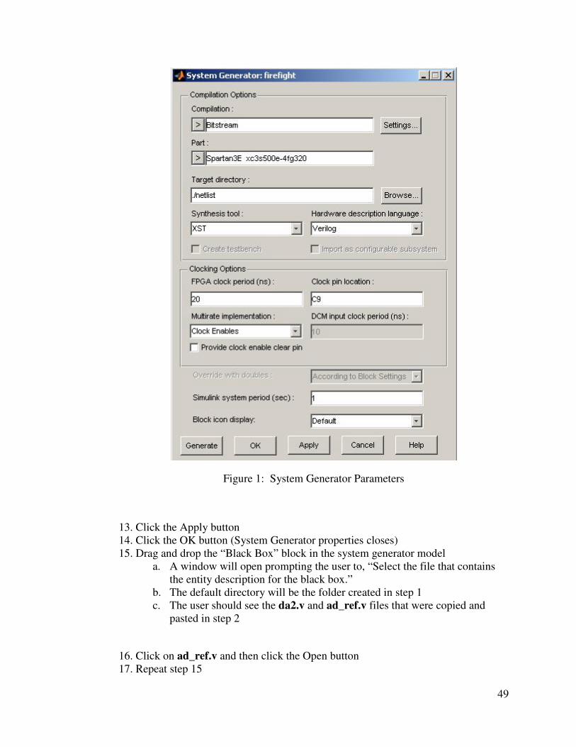
49
Figure 1: System Generator Parameters
13. Click the Apply button 14. Click the OK button (System Generator properties closes) 15. Drag and drop the “Black Box” block in the system generator model
a. A window will open prompting the user to, “Select the file that contains the entity description for the black box.”
b. The default directory will be the folder created in step 1 c. The user should see the da2.v and ad_ref.v files that were copied and
pasted in step 2
16. Click on ad_ref.v and then click the Open button 17. Repeat step 15

50
18. Click on da2.v and then click the Open button a. The user can adjust the sizes of the black boxes to their preference
19. Drag and drop one “Gateway In” block and two “Gateway Out” blocks from the “Basic Elements” library into the new model
20. Connect the “Gateway In” block to the j2_in port on the black box 21. Connect one of the “Gateway Out” blocks to the j2_out port and the other block
to the j1_out port on the black boxes 22. Rename the “Gateway In” and “Gateway Out” ports to the names of the ports they
are connected to a. Double-click on the text label “Gateway In” or “Gateway Out” b. Rename accordingly
23. Verify steps 17-20 by using figure 2
Figure 2: Basic System Generator Model with Black Boxes
24. Double-click on the j2_in “Gateway In” port and change the settings to match those in figure 3
25. Double-click on the j2_out “Gateway Out” port and change the settings to match those in figure 4

51
26. Double-click on the j1_out “Gateway Out” port and change the settings to match those in figure 5
Figure 3: j2_in Properties for ADC

52
Figure 4: j2_out Properties for ADC

53
Figure 5: j1_out Properties for DAC
27. Based on your application, place blocks from the Xilinx Blocksets in the system generator model and connect them between the ‘a2d_data’ port and ‘daval’ port
Generate .bit file to download to FPGA:
1. Double-click on the “System Generator” block within the simulink model 2. Click the “Generate” button (time to complete depends on application) 3. …<folder_from_step1>\netlist\<model_name>_cw.bit 4. Download .bit file to FPGA (multiple ways to do this…more to come) 5. Batch file created to automate this procedure
a. Must change <filename> manually before running b. Must move batch file to directory of .bit file

54
NOTE: The output and input of the ‘a2d_data’ port and ‘daval’ port is unsigned
12-bit (values ranging from 0-4095). Moreover, the input to the PMOD A/D1
module should be between 0-3.3VDC.