A Study of Implementation of Digital Signal Processing for Adaptive Array Antenna · 2002-02-25 ·...
73
MASTER THESIS A Study of Implementation of Digital Signal Processing for Adaptive Array Antenna Supervisor: Associate Prof. Hiroyuki ARAI Submitted on Feb. 12, 2002 Division of Electrical And Computer Engineering, Yokohama National University, Japan 00DD901 Minseok Kim
Transcript of A Study of Implementation of Digital Signal Processing for Adaptive Array Antenna · 2002-02-25 ·...

MASTER THESIS
A Study of Implementation of Digital Signal Processing for Adaptive Array Antenna
Supervisor: Associate Prof. Hiroyuki ARAI Submitted on Feb. 12, 2002
Division of Electrical And Computer Engineering, Yokohama National University, Japan
00DD901 Minseok Kim
ii
PREFACE
An adaptive array antenna technology is paid attention to a lot of applications in the next
generation wireless mobile communications. This technology can form a beam pattern at an
intended direction by applying digital signal processing algorithms to the digitized signals from
each antenna element. It has had some barriers in commercial uses due to implementation
complexities and impractically high costs, but advances in digital device technologies have led to
solve the implementation difficulties due to the nonlinearity of an analog device with a digital
signal processing.
This paper describes the development of an evaluation prototype system for adaptive array
antenna test bed to realize reasonable cost and high performance. And then it presents the
examination of their applications. This paper consists of 3 main parts: first, a design of digital
prototype system; second, a beamforming antenna as an application; third, a DOA (Direction Of
Arrival) estimation system as the other application.
In Chapter 2 the hardware configuration and the design of the digital prototype board that we
developed considering the architecture of software defined radio (SDR) are described. In Chapter 3
and Chapter 4 the examinations of the application implementation using this prototype system are
discussed. Chapter 3 presents the beamforming technique by MRC (Maximum Ratio Combining).
It recombines the output power at maximal ratio by co-phasing received signals at each element
like a phased array antenna. In this chapter, the circuit implementation details and the experimental
results are presented. The digital calibration methods of errors in adaptive array antenna system
caused by non-ideal antenna pattern, mutual coupling between each element and etc are proposed
and the circuit implementations of them are also presented. On the other hand, Chapter 4 deals with
the implementation issue of DOA estimation problem. As a matter of fact, it is significant to
recognize previously the transmission conditions and the environment of radio wave so as to model
a multi-signal propagation efficiently and form beampattern properly. Moreover to form beams at
some directions, most of beamforming algorithms need the knowledge of DOAs of incident waves
in advance. Generally the DOA algorithm is very complex and has heavy computational load. From
this point of view, the high performance DOA estimation system is very useful in the array antenna
technology. In Chapter 4 the hardware implementation of MUSIC (MUltiple SIgnal Classification)
method, a super-resolution DOA estimation method, is discussed. Especially the EVD (Eigen
Value Decomposition) process that takes the largest computational load in the whole system is
mainly focused and the circuit configuration, the estimate of circuit scale and the expected
performance are examined.
Finally, Chapter 5 summarizes and concludes this paper.

iii
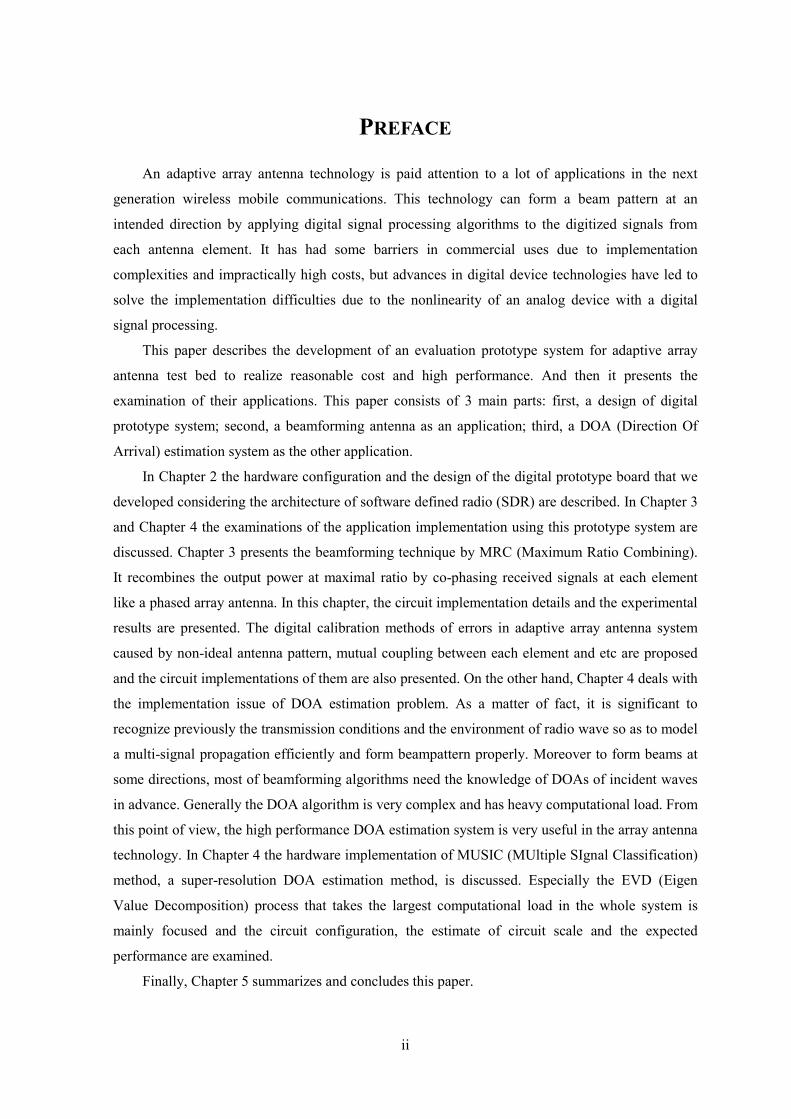
TABLE OF CONTENTS
CHAPTER 1 INTRODUCTION............................................................................................................................ 1
1.1 BACKGROUND..................................................................................................... 1
1.2 SURVEY OF ADAPTIVE ANTENNA ........................................................................ 2 1.2.1 Overview ........................................................................................................................ 2 1.2.2 Basic Configuration and Principle ................................................................................. 3 1.2.3 Performance Improvements ........................................................................................... 5
1.3 OBJECTIVE AND STRUCTURE OF PAPER .............................................................. 6
1.4 IMPLEMENTATION ISSUES ON ADAPTIVE ARRAY SIGNAL PROCESSING AND FPGA (FIELD PROGRAMMABLE GATE ARRAY) ......................................................................... 7
1.4.1 Basic Descriptions of an FPGA...................................................................................... 7 1.4.2 Digital Signal Processing on FPGAs.............................................................................. 9
CHAPTER 2 DESIGN OF DIGITAL PROTOTYPE OF ADAPTIVE ANTENNA RECEIVER ...................11
2.1 INTRODUCTION..................................................................................................11
2.2 ARCHITECTURES OF ADAPTIVE ANTENNA SYSTEM ............................................12 2.2.1 Baseband Sampling Architecture ................................................................................. 12 2.2.2 IF (Intermediate Frequency) Sampling Architecture.................................................... 13 2.2.3 Future Trends and Software Defined Radio (SDR)...................................................... 14
2.3 DEVELOPMENT OF PROTOTYPE SYSTEM............................................................14 2.3.1 System Configuration................................................................................................... 14 2.3.2 Digital Down Conversion (DDC) / Quasi Coherent Detection .................................... 18 2.3.3 NCO and Mixer............................................................................................................ 19 2.3.4 Lowpass Filter .............................................................................................................. 20
2.4 EXAMINATION OF ANALOG TO DIGITAL SAMPLING SCHEMES ............................22 2.4.1 Oversampling Scheme.................................................................................................. 22 2.4.2 Undersampling Scheme................................................................................................ 23
2.5 SUMMARY ..........................................................................................................25 CHAPTER 3 EXAMINATION OF APPLICATIONS IMPLEMENTATION: MRC BEAMFORMING ANTENNA ...................................................................................................................................... 26
3.1 INTRODUCTION..................................................................................................26
3.2 2-ELEMENT MRC BEAMFORMING ANTENNA.....................................................26
3.3 HARDWARE IMPLEMENTATION...........................................................................29 3.3.1 Weight Calculation / MRC (Maximum Ratio Combining) Processor.......................... 29 3.3.2 Circuit Design / Logic Synthesis (Scale of Circuit) ..................................................... 31
iv
3.4 EXPERIMENTAL RESULTS ..................................................................................32 3.4.1 DOA Estimation and DOA Tracking............................................................................ 34 3.4.2 Discussion .................................................................................................................... 38
3.5 EXAMINATION OF DIGITAL CALIBRATION OF ARRAY ANTENNA ..........................40 3.5.1 Adjustment by NCO Control........................................................................................ 40 3.5.2 Adjustment by Maximal Ratio Combining (MRC)...................................................... 42 3.5.3 Discussion .................................................................................................................... 44
3.6 SUMMARY ..........................................................................................................44 CHAPTER 4 EXAMINATION OF APPLICATIONS IMPLEMENTATION: DOA ESTIMATION BY MUSIC METHOD........................................................................................................................................ 45
4.1 INTRODUCTION..................................................................................................45
4.2 PERFORMANCE REQUIREMENT..........................................................................46
4.3 DOA ESTIMATION USING MUSIC METHOD ......................................................47
4.4 HARDWARE IMPLEMENTATION OF DOA ESTIMATOR USING MUSIC METHOD ..49
4.5 DESIGN OF EVD PROCESSOR USING JACOBI METHOD BASED ON CORDIC ALGORITHM .................................................................................................................50
4.5.1 Cyclic Jacobi Method................................................................................................... 50 4.5.2 CORDIC (COordinate Rotation DIgital Computer) Algorithm for Computing Vector Rotation.................................................................................................................................... 52 4.5.3 Examination of CORDIC-Jacobi EVD Processor with Fixed Point Operation ........... 58 4.5.4 Hardware Design of EVD Processor............................................................................ 61 4.5.5 Circuit Scale / Expected Performance.......................................................................... 63 4.5.6 Discussion .................................................................................................................... 63
4.6 SUMMARY ..........................................................................................................64 CHAPTER 5 SUMMARY AND CONCLUSION ............................................................................................... 65 ACKNOWLEDGMENTS ............................................................................................................. 66 BIBLIOGRAPHY .......................................................................................................................... 67 PUBLICATION LIST.................................................................................................................... 69
1
Chapter 1
Introduction
1.1 Background Wireless Communication technologies have a great progress in recent years and the markets,
especially the cellular telephone, have been growing enormously. Moreover the next generation
communication services will use higher frequency band area and require more channel capacity
and wider bandwidth for a high-speed data communication. As a large increase in channel capacity
and high transmission rates for wireless communications, the technologies for the power saving and
efficient frequency usability are required.
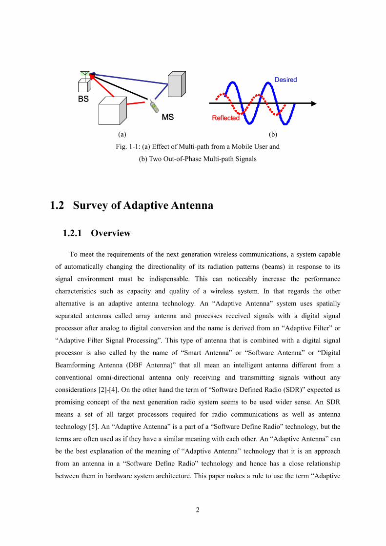
As a matter of fact in many communication environments there are several serious problems
such as a multi-path fading caused by a reflection by any physical structures as Fig. 1-1(a). When
passing through multi-path, the signals are delayed and out of phase from the signals through
direct-path, as shown in Fig. 1-1(b) that causes the signal strength to be weakened at a receiver and
hence receiving quality is also reduced. Generally it is known as “Raleigh Fading”. Wider band and
higher transmission rate make it more critical problem in the improvement of the communication
quality in the next generation communication. To solve this problem many solutions have been
studied. However it is very important to configure receiver and transmitter flexibly in response to
the signal environment recognizing spatial profiles as well as temporal ones. For example spatial
diversity techniques using composite information from the array to minimize fading and other
undesirable effects of multi-path propagation have been studied in many applications. Several
techniques such as phased array antenna and diversity antenna using active array configurations
can adapt the antenna pattern according to the change of mobile communication environment.
However these analog-based techniques have any unavoidable problems that are related to difficult
control, absence of individual beam shape control, complex scheme and corresponding heavy
equipment and so forth [1].
2
BS
MS
BS
MS
Desired
Reflected
Desired
Reflected
(a) (b)
Fig. 1-1: (a) Effect of Multi-path from a Mobile User and
(b) Two Out-of-Phase Multi-path Signals
1.2 Survey of Adaptive Antenna
1.2.1 Overview
To meet the requirements of the next generation wireless communications, a system capable
of automatically changing the directionality of its radiation patterns (beams) in response to its
signal environment must be indispensable. This can noticeably increase the performance
characteristics such as capacity and quality of a wireless system. In that regards the other
alternative is an adaptive antenna technology. An “Adaptive Antenna” system uses spatially
separated antennas called array antenna and processes received signals with a digital signal
processor after analog to digital conversion and the name is derived from an “Adaptive Filter” or
“Adaptive Filter Signal Processing”. This type of antenna that is combined with a digital signal
processor is also called by the name of “Smart Antenna” or “Software Antenna” or “Digital
Beamforming Antenna (DBF Antenna)” that all mean an intelligent antenna different from a
conventional omni-directional antenna only receiving and transmitting signals without any
considerations [2]-[4]. On the other hand the term of “Software Defined Radio (SDR)” expected as
promising concept of the next generation radio system seems to be used wider sense. An SDR
means a set of all target processors required for radio communications as well as antenna
technology [5]. An “Adaptive Antenna” is a part of a “Software Define Radio” technology, but the
terms are often used as if they have a similar meaning with each other. An “Adaptive Antenna” can
be the best explanation of the meaning of “Adaptive Antenna” technology that it is an approach
from an antenna in a “Software Define Radio” technology and hence has a close relationship
between them in hardware system architecture. This paper makes a rule to use the term “Adaptive

3
Antenna” from the point of view that it applies digital signal processing technology to the antenna
adaptively.
An adaptive antenna can form a beam pattern at an intended direction by applying digital
signal processing algorithm with the digitized data from each antenna element. By software
algorithm this system at the transmitter is capable of steering the maximum radiation pattern
toward a desired mobile and the system at the receiver can spatially separate and reject multi-path
fading energy hence higher bit rate services can be provided [6]. Despite of these advantages, there
are some obstacles in commercial uses due to implementation complexities and impractically high
costs.
1.2.2 Basic Configuration and Principle
Generally an adaptive antenna system consists of a lot of functions including an array antenna
and an RF (Radio Frequency) and IF (Intermediate Frequency) circuitry and beamforming network
and an adaptive controller. Fig. 1-2 illustrates the basic configuration. An array antenna is plural
number of antennas designed to receive or transmit signals using the combined beampattern. There
are various physical arrangements of an array such as linear, circular, rectangular, and etc. The
structure of an array antenna is determined in consideration of the characteristics and the
applications. Most functions of the RF/IF circuitry are frequency downconversion, filtering and
amplifying. The beamforming network performs a phase and amplitude control of input signals fed
from array antenna, which plays a role in combining beampattern of the array antenna operating as
a spatial filter. An adaptive controller determines the optimum weight for beamforming. There are
various algorithms for obtaining optimum weight. In an adaptive antenna system, the complex
structure, heavy hardware, difficulty to reconstruct and maintenance, etc. with analog technologies
come to need the alternative solution. Therefore the configuration using digital technologies has
lately considerable attention.
#1#2# M
⋅⋅⋅⋅⋅⋅
AdaptiveController
Output
⋅⋅⋅⋅⋅⋅
Weight W1
WM
Fig. 1-2: Diagram of Basic Adaptive Antenna System

4
•••
θ
d
)(NxM )(2 Nx )(1 Nx
Incident wave)(Ns
wavefront
dM )1( −
θsin)1( dM −
Fig. 1-3: Uniform Linear Array of M-Element
The basic structure to explain the principle of adaptive antenna signal processing is illustrated
by Fig. 1-3. The array antenna is assumed to be a uniform equidistance linear array of identical and
omni-directional M elements and an electromagnetic wave arriving at array antenna is an
approximately plane and narrowband signal. Let the angle between wave normal and incident angle
θ, the far-field expression of the electrical signal at k-th element at any discrete time N is given by
)sin2exp()()( θλπ dkjNsNx kk −⋅=
Mk ,,2,1=
(1.1)
where sk(N), λ and θ is the envelop, wavelength and Direction-Of-Arrival (DOA) angle of an
incident wave respectively and d is the distance spaced between each antenna. In this equation if
sk(N) is a narrow band signal the temporal delay caused by different path between elements
corresponds to the phase difference. The output of array antenna is produced by the inner product
(multiply-accumulate operation) of input signals and weight coefficients determined by adaptive
algorithms as (1.2).
∑=
−⋅⋅=M
kkk dkjNswNy
1
* )sin2exp()()( θλπ
(1.2)
They can be also re-written by vector expression as (1.3)-(1.4).
])()()([ 21 NxNxNx MT=X
(1.3)
XW=y H (1.4)
Basically adaptive antenna technique forms the antenna radiation pattern toward intended
direction by digital signal processing. There are two kinds of work. One is beam-steering toward
desired direction and the other is null-steering toward undesired interferences, which may be more
important function and the original concept of an adaptive antenna. Furthermore historically the

5
first adaptive antenna is Howells’ intermediate frequency (IF) side-lobe canceller for nulling out
the effect of one jammer.
On the other hand, to determine the optimum weight, most of the beamforming algorithms
such as MMSE (Minimizing Mean Square Error), MSN (Maximizing Signal to Noise ratio),
LCMV (Linearly Constrained Minimum Variance Filter), etc. whose solutions are based on solving
Wiener-Hopf equation require the information of DOAs of desired signals and interferers in
advance. Of course, there are also blind methods in which the information of DOAs is not
necessary such as CMA (Constant Modulus Algorithm). As a matter of fact it is significant to
recognize previously the transmission conditions and the environment of radio wave. That is to say,
the spatial profile such as DOAs of incident signals as well as the temporal profile such as their
frequency characteristics is needed. Therefore various techniques of DOA estimation are studied
also as a part of adaptive antenna technologies [7].
1.2.3 Performance Improvements
Array signal processing is capable of forming transmit/receive beams towards the desired
mobile. At the same time it is possible to place spatial nulls in the direction of undesired
interferences called null-steering. This capability can be used to improve the performance of a
mobile communication system as follows. The adaptive antenna has a higher gain than a
conventional omni-directional antenna. The higher gain can be used to either increase the effective
coverage, or to increase the receiver sensitivity. Conversely it can be exploited to reduce transmit
power and electromagnetic radiation in the communication network. Multi-path propagation in
mobile radio environments leads to inter-symbol-interference (ISI). Using transmit and receive
beams that are directed towards the desired mobile reduces the adverse effects of multi-path and
ISI. Adaptive antenna transmitters emit less interference by only sending RF power in the desired
directions. Furthermore, adaptive antenna receivers can reject interference by looking only in the
direction of the desired source. Consequently adaptive antennas are capable of decreasing
co-channel-interference (CCI) [8].

6
1.3 Objective and Structure of Paper This paper focuses on the implementation issues of an adaptive antenna and examines its
applications for practical uses. Historically an adaptive antenna has been mainly used for military
applications, but recently practical uses for various applications in wireless communications are
expected. However there are many obstacles to realize an adaptive antenna system such as
implementation complexity and impractically high cost. The main concept of an adaptive antenna
is the automatic or adaptive control of antenna’s beampattern by digital signal processing with a
software algorithm. An important requirement to realize in current or next generation
communications is high-speed realtime processing. But until now the performance of digital
devices such as general DSP (Digital Signal Processor) or MPU (Micro Processing Unit) for array
signal processing is so poor as to unable to process a large-scale computation and they also
consume inefficiently large power to be unsuitable for mobile communications. On the other hand
using high performance specific LSI called ASIC (Application Specific Integrated Circuit) bring a
low flexibility. A digital device capable of high-speed realtime processing, consuming low power
and programmable is required for practical use of an adaptive antenna in wireless communications.
In recent year using an FPGA (Field Programmable Gate Array) for the implementation of an
adaptive antenna meets the requirements of high performance processing, programmability and low
power consumption. It is described in the next section in detail.
This paper examines the practical implementations of an adaptive antenna technique using
FPGAs as a digital signal processor. The design and development of a digital prototype system for
the evaluation of an adaptive antenna technology are described in Chapter 2 and the application
implementations are examined in Chapter 3 and Chapter 4. Beamforming and DOA estimation
technique are two typical applications of an adaptive antenna technology. In Chapter 3 the
implementation of simple Maximal Ratio Combination (MRC) beamforming antenna and this
chapter also discusses a digital calibration techniques of an array antenna system. In Chapter 4
DOA estimation technique using MUSIC (MUltiple SIgnal Classification) algorithm are described
and Chapter 5 concludes this paper.
7
1.4 Implementation Issues on Adaptive Array Signal Processing And FPGA (Field Programmable Gate Array)
There are many requirements needed for implementation of an adaptive antenna technology in
the next generation wireless communication system. From the point of view that adaptive antenna
is a new concept of antenna combining with digital signal processing unit, the most critical thing
can be the performance of a digital signal processor. In other words the high performance for
realtime processing of a large-scale computation has been the highest barrier to implement.
Considering applications for mobile communication the solution of power consumption problem is
also required. In addition reconfigurablity or programmability can improve the communication
quality extremely recognizing the communication environment and reconstructing the optimum
configuration adaptively, which is a concept of software defined radio.
Particularly to meet the requirement of the real-time processing performance in adaptive
antenna techniques takes a complex and high cost array antenna network and a high performance
DSP (Digital Signal Processor). Hence in the past they were examined only academically and
developed for only special uses such as military radar applications. As the technologies of VLSI
have made a great progress nowadays, the processing speed is getting faster and the integration
scale is getting larger. SRAM-based FPGA (Field Programmable Gate Array) technology has led to
another alternative solution for digital signal processing. In this paper, the system implemented by
using an FPGA is introduced. FPGAs in this system play a part as a digital signal processor for
digital beamforming or DOA (Direction Of Arrival) estimation functions, which require a large
number of MAC (Multiply-ACcumulate) operations and need large-scale parallel processing.
FPGAs can meet these requirements.
1.4.1 Basic Descriptions of an FPGA
A programmable logic device (PLD) is loosely defined as a device with configurable logic and
flip-flop linked together with programmable interconnect as shown in Fig. 1-4. An FPGA is a kind
of programmable logic devices and an array of gates with programmable interconnect and logic
functions. It can be reconfigured infinite times after manufacture but generally distinct from PLD
by higher logic capacity. An FPGA consists of logic blocks and an interconnection resource to
connect the logic blocks. The logic block usually contains lookup tables (LUTs) and flip-flops
(FFs) to store data as Fig. 1-5. Input ports are connected to LUT input ports or FF input ports and
outputs from LUTs are either connected to output ports of the logic block or connected to FF input

8
ports. By using multiplexing, various combinations of inputs can be chosen and sequential logics
with memory element of FF as well as combinational logics with LUTs are also available [12].
To integrate complex logic circuits distributed to lots of LSI’s on board by single or more
devices, programmable logic devices have been mainly used. A progress of device integration
technology can provide to implement more complex circuits such as large-scale digital signal
processing on single FPGA. Furthermore it has many advantages over the other digital signal
processing solutions as DSP or MPU and ASIC. The next section describes the advantages in
detail.
Fig. 1-4: Structure of an FPGA
LE OutLook-up
Table
(LUT)
CascadeChain
PRND Q
CLK
CLRN
DATA1
DATA2
DATA3
DATA4
Cascade In
CascadeOut
Load Pre-ComputedLogic
Cascade&
CarryChain
Carry In
CarryOut
1 0 1 00 0 1 11 1 0 01 1 1 0
1 0 1 00 0 1 11 1 0 01 1 1 0
Fig. 1-5: FPGA Logic Block

9
1.4.2 Digital Signal Processing on FPGAs
As mentioned before, there are a few kinds of digital signal processing solutions for array
signal processing techniques. One is using a general purposed processor (DSP or MPU), and the
other one is using an ASIC (Application Specific Integrated Circuit). While general purposed
processor solutions are very flexible because their architectures are optimized to process a fixed set
of instructions but may not be ideally suited to the specific application, ASIC solutions offer the
ability to design a custom architecture that is optimized for a particular application. For example, a
general purposed conventional DSP has only single multiply-accumulate (MAC) stage, so the
computations must be executed sequentially, namely in serial, but whereas an ASIC
implementation can have multiple parallel Multiply-ACcumulate (MAC) stages. When comparing
the performance of the ASIC versus the general purposed DSP, it becomes apparent that the DSP
or MPU offers slow speed but maximum flexibility (programmability) while the ASIC provides
high speed with minimal flexibility.
On the other hand, an FPGA combines the versatility of a programmable solution with the
performance of dedicated hardware as shown in Fig. 1-6. An FPGA can obtain the true goal of
parallel processing executing algorithms with the inherent parallelism due to distributed arithmetic
structure while avoiding the instruction fetch and load/store bottlenecks of traditional Von
Neumann architectures [11]-[13].
DSP On FPGA
DSP DSP On FPGAOn FPGA
Flexibility
Performance
DSPProcessor
DSPDSPProcessorProcessor
ASSPsASSPsASSPs ASICsASICsASICs
Flexible, But LacksReal-Time Performance
Flexibility of DSP, with Performance of ASIC
High Performance,but Inflexible
Fig. 1-6: FPGAs offer both Flexibility and Performance

10
Implementing DSP function in FPGA devices provides the following advantages as Table 1-1
[12]. FPGAs are thought as a key device in implementation of an adaptive antenna or a software
defined radio thanks to their high performance, flexibility and reconfigurablity and etc.
TABLE 1-1 A COMPARISON OF FPGA AND DSP PROCESSOR
FPGA DSP
Programmable Language VHDL, Verilog C, Assembly
Ease of S/W programming Fairly easy but needs
understanding the hardware architecture
Easy
Performance Very fast if optimized Speed depends on operating clock
speed Reconfigurablity/ Programmability
SRAM-type FPGAs can be reconfigured infinite times
Re-programmable by changing program
Outperforming Area Digital Filters, FFT, etc Sequential processing
Power Consumption Can be minimized if circuit is
optimized Cannot optimize
Implementation Method of MAC
Parallel and distributive arithmeticRepeat operation of one or a few
MACs
Speed of MAC Can be fast if a parallel algorithmDepends on operation clock
speed
Parallelism Can be parallelized for high
performance Usually sequential and cannot be
parallelized
11
Chapter 2
Design of Digital Prototype of Adaptive Antenna Receiver
2.1 Introduction An adaptive antenna system is a compound technology of many components. As increasing
the number of antenna elements, accordingly the system scale gets huger. An adaptive antenna
system performs the analog functions of frequency conversion, filtering, gain control and the
digital functions of adaptive signal processing, modulation/demodulation and etc after or before
A/D or D/A conversion. It is very significant to consider the architecture that provides low costs
but meets the performance requirements when designing an adaptive antenna system.
In this chapter, the architectures of an adaptive antenna system are discussed. And the design
and development of digital prototype evaluation system on which adaptive antenna techniques are
implemented are described. This chapter deals with the implementation of only digital part of IF
and baseband stages except analog RF stages. The digital part consists of analog to digital
converters (ADCs), FPGAs as a digital signal processor and a CPU for the control of the whole
system. This chapter presents the circuit configuration and IF signal processing such as digital
downconversion on FPGAs. In addition the relationship to software defined radio architectures
through the study of sampling schemes and signal processing on FPGAs is discussed.

12
2.2 Architectures of Adaptive Antenna System There are many ways of classifying the architectures of an adaptive antenna system. One of
them is the way that how many downconversion stages it has. This way can classify a direct
conversion with only single downconversion stage at RF into baseband and a super-heterodyne
with a few downconversion stages at RF into baseband via IF. Another is the way that where the
ADCs (Analog to Digital Converters) are placed. Generally, the position of ADCs is the most
dominant factor of system architecture.
This chapter discusses two types of architectures according to the placement of an ADC. One
is a baseband sampling architecture and the other is an IF (Intermediate Frequency) sampling
architecture. In addition future trends and the architecture of software defined radio are discussed.
2.2.1 Baseband Sampling Architecture
As shown in Fig. 2-1, it has a few downconversion stages and baseband I/Q signals are
derived from mixing the last IF signal with a reference local oscillator. Because the ADC is placed
at baseband, the system does not require a high speed and high performance ADC. Usually this
system architecture has been used as direct downconversion, double downconversion and triple
downconversion according to the number of downconversion stages. Direct conversion has many
problems to realize such as a difficulty of building filters to meet the phase and amplitude matching
requirements but is attractive from a system downsizing point of view with less RF components.
Additional mixers can be added to the direct conversion architecture to improve performance and
stability and usually the triple downconversion architecture has been used. This architecture can
allow the second IF frequency to be sufficiently low so that a bandpass filter such as a surface
acoustic wave (SAW) filter, can be used to define the signal bandwidth. This filter has very low
phase and amplitude distortion and hence can provide the high performance. The architectures
mentioned above have the analog downconversion stage as the detection of I/Q baseband signals.
That causes a few problems as following [14]
Poor matching between the characteristics of the I/Q signals
Impairment of I/Q orthogonality
DC offset
Spurious noise due to the nonlinearity of the analog components

13
LNAAdaptive
ProcessingAdaptive
Processing
MixerIF
Amp.
VideoAmp.
VideoAmp.
0o 90o
LO1
LO2
I
Q
A/DA/D
A/DA/D
Dem
odulationD
emodulation
I
Q
DigitalAnalog
BPF
LPF
LPF
Fig. 2-1: Receiver Architecture with Baseband Sampling
2.2.2 IF (Intermediate Frequency) Sampling Architecture
The alternative conversion architecture is shown in Fig. 2-2. This architecture digitizes signals
at IF directly and the complex video signal is generated digitally. In this architecture, the analog
mixer and lowpass filters are replaced with digital techniques. Only one high speed ADC provides
with decreasing the system circuitry. In addition, the linearity of digital filters solves the matching
problems between I/Q signals [14]. A digital downconverter (DDC) is required to perform the
coherent detection function. It consists of an NCO (Numerical Controlled Oscillator), a pair of
multipliers (mixers in analog sense), lowpass filters and decimations. The decimation reduces data
rates which means extracting the narrow baseband signal from the wideband IF input signal. This
can allow the digital signal processor to operate at moderate speed. This approach requires the high
speed and wide bandwidth ADC and high performance digital multipliers and filters.
Decimation
)cos( nc ⋅ω
)sin( nj c ⋅− ω
NCOA/DA/D
NCO : Numerical Control Oscillator
LNA
Mixer
IFAmp.
LO
AdaptiveProcessingAdaptiveProcessing
I
Q
Dem
odulationD
emodulation
I
Q
DigitalAnalogDigital Down Converter
/ Quasi-Coherent Detector
BPF
LPF
LPF
LPF
Fig. 2-2: Receiver Architecture with IF Sampling and DDC

14
2.2.3 Future Trends and Software Defined Radio (SDR)
In the next steps, the ideal architecture as shown in Fig. 2-3 is promising. This approach
places an ADC toward antenna as close as possible. Antenna and RF front-end are required to be
suitable for receiving wideband signal and ADC must be also able to digitize wide band signal at
sampling rates. The other radio functions such as IF, baseband and bit stream processing are carried
out using programmable digital processor like a DSP or an FPGA. This is the concept of a software
defined radio (SDR). By using programmable or reconfigurable digital signal processing devices
multi-mode and multi-band services can be provided and by applying adaptive antenna signal
processing it is possible to maximize the system performance and optimize the communication
environment.
RFFrontend
WidebandADC
ProgrammableProcessor
IQ
WidebandAntenna
Fig. 2-3: Software Defined Radio Concept
2.3 Development of Prototype System A few available architectures of an adaptive antenna system were discussed in the previous
section. The IF sampling architecture has many advantages over the baseband sampling. The digital
downconversion must be the key process to realize a system toward a software defined radio. This
section introduces the digital prototype system of IF sampling architecture, which performs I/Q
detection digitally on FPGAs.
2.3.1 System Configuration
The digital prototype evaluation system is developed to apply to various adaptive antenna
signal processing. It consists of ADC board with ADCs (SPT7938, SPT), and CPU board with a
CPU (SH4, HITACH) as a controller. Fig. 2-4 shows the photographs. An ADC board has 2
channels of ADC, buffer memory and 3 FPGAs (total about 300,000 equivalent gates). The CPU
board that has CPU, SH4 operating at 200MHz and whose operating system is NetBSD, plays a
part in ADC control and as a numerical computation coprocessor. It also offers monitoring
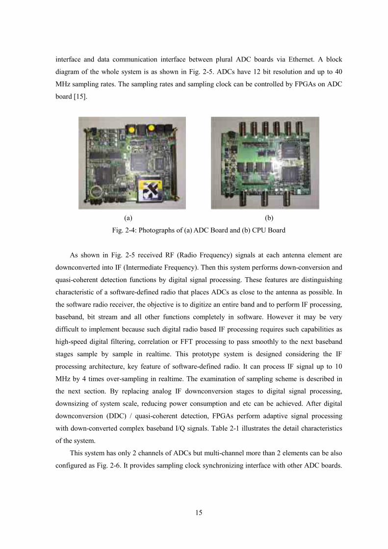
15
interface and data communication interface between plural ADC boards via Ethernet. A block
diagram of the whole system is as shown in Fig. 2-5. ADCs have 12 bit resolution and up to 40
MHz sampling rates. The sampling rates and sampling clock can be controlled by FPGAs on ADC
board [15].
(a) (b)
Fig. 2-4: Photographs of (a) ADC Board and (b) CPU Board
As shown in Fig. 2-5 received RF (Radio Frequency) signals at each antenna element are
downconverted into IF (Intermediate Frequency). Then this system performs down-conversion and
quasi-coherent detection functions by digital signal processing. These features are distinguishing
characteristic of a software-defined radio that places ADCs as close to the antenna as possible. In
the software radio receiver, the objective is to digitize an entire band and to perform IF processing,
baseband, bit stream and all other functions completely in software. However it may be very
difficult to implement because such digital radio based IF processing requires such capabilities as
high-speed digital filtering, correlation or FFT processing to pass smoothly to the next baseband
stages sample by sample in realtime. This prototype system is designed considering the IF
processing architecture, key feature of software-defined radio. It can process IF signal up to 10
MHz by 4 times over-sampling in realtime. The examination of sampling scheme is described in
the next section. By replacing analog IF downconversion stages to digital signal processing,
downsizing of system scale, reducing power consumption and etc can be achieved. After digital
downconversion (DDC) / quasi-coherent detection, FPGAs perform adaptive signal processing
with down-converted complex baseband I/Q signals. Table 2-1 illustrates the detail characteristics
of the system.
This system has only 2 channels of ADCs but multi-channel more than 2 elements can be also
configured as Fig. 2-6. It provides sampling clock synchronizing interface with other ADC boards.
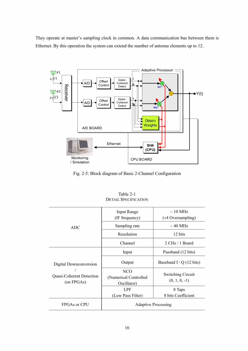
16
They operate at master’s sampling clock in common. A data communication bus between them is
Ethernet. By this operation the system can extend the number of antenna elements up to 12.
W1*
W2*
Y(t)
A/DA/D
A/DA/D
Receiver
Receiver
#1
#2
)(1 tx
)(2 tx
Quasi-Coherent
Detect
Quasi-Coherent
Detect
I
Q
ObtainWeightsObtain
Weights
I
Q
SH4(CPU)SH4
(CPU)
A/D BOARD
Monitoring/ Simulation
Ethernet
OffsetControlOffsetControl
OffsetControlOffsetControl
Quasi-Coherent
Detect
Quasi-Coherent
Detect
CPU BOARD
Adaptive Processor
Fig. 2-5: Block diagram of Basic 2-Channel Configuration
Table 2-1 DETAIL SPECIFICATION
Input Range (IF frequency)
~ 10 MHz (x4 Oversampling)
Sampling rate ~ 40 MHz
Resolution 12 bits ADC
Channel 2 CHs / 1 Board
Input Passband (12 bits)
Output Baseband I / Q (12 bits)
NCO (Numerical Controlled
Oscillator)
Switching Circuit (0, 1, 0, -1)
Digital Downconversion /
Quasi-Coherent Detection (on FPGAs)
LPF (Low Pass Filter)
8 Taps 8 bits Coefficient
FPGAs or CPU Adaptive Processing

17
Ch.2
Ch.x
Ch.y
PC
Ch.1
Ethernet
ClockTrigger
….
A/D
A/D FIFO
FPGA CPU(SH4)
MasterFIFO
A/D
A/D FIFO
FPGA CPU(SH4)
SlaveFIFO
Ch.2
Ch.x
Ch.y
PC
Ch.1
Ethernet
ClockTrigger
….
A/D
A/D FIFO
FPGA CPU(SH4)
MasterFIFO
A/D
A/D FIFO
FPGA CPU(SH4)
SlaveFIFO
PC
Ch.1
Ethernet
ClockTrigger
….
A/D
A/D FIFO
FPGA CPU(SH4)
MasterFIFO
A/D
A/D FIFO
FPGA CPU(SH4)
SlaveFIFO
(a)
Master
Slave1
Slave2
#6 #5 CLK
#4 #3 CLK
#2 #1 CLK
Front View
Master
Slave1
Slave2
CLK
Rear View
(b)
DOA EstimationBeamforming
RF
Dem
odula
tionData
Decoding
N Channels )cos( nc ⋅ω
)sin( nj c ⋅− ω
NCOA/DA /D
IF
)(1 nxx I1
x Q1Decimation
LPF
LPF
w I1
w Q1I/Q-Detection
)cos( nc ⋅ω
)sin( nj c ⋅− ω
NCOA/DA /D
IF
)(2 nxDecimation
LPF
LPF
w I2
w Q2I/Q-Detection
x I2
x Q2
(c)
Fig. 2-6: (a) Control via Ethernet, (b) 6-element Configuration and (c) Block Diagram of
Multi-channel Configuration

18
2.3.2 Digital Down Conversion (DDC) / Quasi Coherent Detection
Digital Down Conversion / Quasi-coherent detection is implemented by using NCO
(Numerical Control Oscillator), mixer and lowpass filters as shown in Fig. 2-7. It consists of
sinusoidal signal generator by NCO and 2 FIR (Finite Impulse Response) lowpass filters, where ωc
is angular carrier frequency. If a sampling frequency is 4 times of IF center frequency, NCO and
mixer can be easily implemented. In this paper, NCO and mixer are simply implemented by
sequence switching circuit (0, 1, 0, -1) as shown in Fig. 2-8. The FIR filters of 8 taps are used.
In digitizing the analog received signals at IF (Intermediate Frequency) only one ADC is
required for each antenna element so it can make the system scale by half. In this part, digital signal
processing downconvert the sampled bandpass signals from ADC into a complex baseband signal
[16]. Bandpass signals can be expressed as a sum of two quadrature components which are π/2 out
of phase. Generally bandpass signal is represented by
nwnxnwnxnx cQcI sin)(cos)()( += , (2.1)
where xI(n) is the in phase component, xQ(n) is the quadrature component of the signal x(n) and ωc
is the center frequency of the band pass signal (carrier frequency). The downconversion process
shifts the carrier frequency ωc to baseband. It performs multiplication of the incoming bandpass
signal x(n) with the complex phasor [cosωcn- sinωcn] and then lowpass filters the result as (2.2).
]2cos)(2sin)()(
2sin)(2cos)()([21
]sin)[cos()(
nwnxjnwnxnxj
nwnxjnwnxnx
nwnwnxnx
cQcQQ
cIcII
cc
++−
+−+=
−=′
(2.2)
This operation accomplishs the desired frequency shift. After lowpass filtering, the second
harmonic components are filtered out and the result is the desired complex baseband signal
representation of x(n) as (2.3) [17].
)]()([21))(( nxjnxnxLPF QI −=′ (2.3)
Fig. 2-7 illustrates the block diagram that represents the frequency spectrum as well as this
mathematical process. Next sections describe the FPGA implementation details.

19
)(nxI
)(nxQ
)cos( nc ⋅ω
)sin( nj c ⋅− ω
NCONCOA/DA/DIF
)(nx NCO : Numerical Control Oscillator
f cf c f c f sf c f s f c f c2f c f c2 Fig. 2-7: Digital Downconversion / Quasi-Coherent Detection
2.3.3 NCO and Mixer
The downconversion process requires an NCO (Numerical Controlled Oscillator) and a mixer
multiplying bandpass signal and digital local sine/cosine signal generated by NCO as shown in Fig.
2-7. There are various methods to implement them. The method generating quadrature signals by
DDS (Direct Digital Synthesizer) is usually used. But if clock signal of exactly N times of carrier
frequency is achievable, the NCO and mixer are no more than a simple switching circuit as Fig.
2-8. This system performs downconversion function at 4 times of carrier frequency of bandpass
signal.
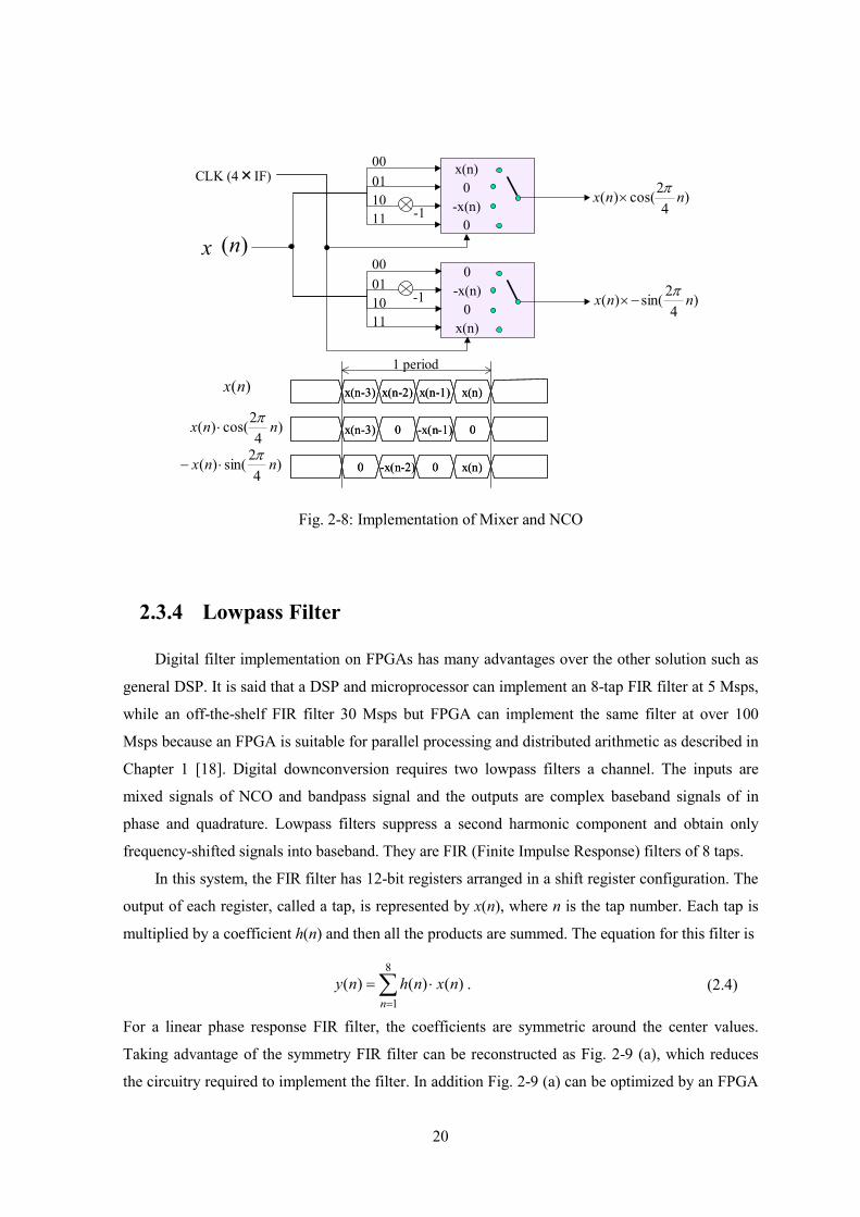
20
x(n)0
-x(n)0
0-x(n)
0x(n)
)(nx
00011011
00011011
-1
-1
)4
2cos()( nnx π⋅
)(nx
)4
2sin()( nnx π⋅−
)4
2cos()( nnx π×
)4
2sin()( nnx π−×
CLK (4××IF)
x(n-3) 0 -x(n-1) 0x(n-3) 0 -x(n-1) 0
1 period
0 -x(n-2) 0 x(n)0 -x(n-2) 0 x(n)
x(n-3) x(n-2) x(n-1) x(n)x(n-3) x(n-2) x(n-1) x(n)
Fig. 2-8: Implementation of Mixer and NCO
2.3.4 Lowpass Filter
Digital filter implementation on FPGAs has many advantages over the other solution such as
general DSP. It is said that a DSP and microprocessor can implement an 8-tap FIR filter at 5 Msps,
while an off-the-shelf FIR filter 30 Msps but FPGA can implement the same filter at over 100
Msps because an FPGA is suitable for parallel processing and distributed arithmetic as described in
Chapter 1 [18]. Digital downconversion requires two lowpass filters a channel. The inputs are
mixed signals of NCO and bandpass signal and the outputs are complex baseband signals of in
phase and quadrature. Lowpass filters suppress a second harmonic component and obtain only
frequency-shifted signals into baseband. They are FIR (Finite Impulse Response) filters of 8 taps.
In this system, the FIR filter has 12-bit registers arranged in a shift register configuration. The
output of each register, called a tap, is represented by x(n), where n is the tap number. Each tap is
multiplied by a coefficient h(n) and then all the products are summed. The equation for this filter is
∑=
⋅=8
1)()()(
nnxnhny . (2.4)
For a linear phase response FIR filter, the coefficients are symmetric around the center values.
Taking advantage of the symmetry FIR filter can be reconstructed as Fig. 2-9 (a), which reduces
the circuitry required to implement the filter. In addition Fig. 2-9 (a) can be optimized by an FPGA

21
using look-up tables (LUTs). The multiplication and addition can be performed in parallel using
LUTs [18]. The characteristics of FIR filter are shown in Fig. 2-10.
X(n-3)
h1 h4h3h2
s1s3s2
m+ws4
m+w+1
Ytm+w+2
x(n+1)D Q D Q D Q D Q
DQDQDQDQ
X(n) X(n-1) X(n-2)
X(n-4)X(n-5)X(n-6)X(n-7)
LOOK UP TABLE(LUT)
Yt
x(n+1)D Q D Q D Q D Q
DQDQDQDQ
X(n) X(n-1) X(n-2) X(n-3)
X(n-4)X(n-5)X(n-6)X(n-7)
(a) (b)
Fig. 2-9: (a) Conventional FIR filter using Symmetry and
(b) FIR Filter using LUT (Look Up Table)
0 0.1 0.2 0.3 0.4 0.5-40
-20
0
20
40
60
Frequency
Mag
nitu
de -
dB
0 0.1 0.2 0.3 0.4 0.5-40
-20
0
20
40
60
Frequency
Mag
nitu
de -
dB
0 1 2 3 4 5 6 70
20
40
60
80
100
120
140Kaiser β=0.5
0 1 2 3 4 5 6 70
20
40
60
80
100
120
140Kaiser β=0.5
Time Step (a) (b)
Fig. 2-10: (a) Time Domain and (b) Frequency Domain Impulse Response of Lowpass Filter

22
2.4 Examination of Analog to Digital Sampling Schemes The system mentioned in previous section provides two schemes of ADC sampling:
oversampling including Nyquist sampling and undersampling (also called subsampling or bandpass
sampling). This section discusses them and examines the application to our system. This prototype
system has the ADC (SPT7938, SPT) which allows a wideband analog input up to 250 MHz and
has the sampling rate up to 40 MHz. The diagram of sampling schemes is illustrated in Fig. 2-11.
BasebandI / Q Signal
Low-IFBandpass Signal
IF Bandpass Signal
Undersampling
DDC
Oversampling IF
Bandpass Signal
fc = 70 MHz
fc = 10 MHz
40 Msps
fc = 10 MHz
fc = 10 MHz
Fig. 2-11: Flows of Each Sampling Scheme
2.4.1 Oversampling Scheme
The sampling rate in analog to digital conversion is determined by Nyquist sampling criterion
which specifies the required sampling rate for signal reconstruction as
ff s max2> , (2.5)
where fs is the sampling rate and fmax is the maximum frequency of a signal to be digitized.
Generally sampling at rates greater than 2fmax is called oversampling. The advantage of this
approach is that the aliase that appears around fs becomes increasingly separated as the sampling
rate fs is increased beyond 2fmax. By sampling at a higher rate, a simpler anti-aliasing filter with a
more moderate transition and less stopband attenuation can be used without any increase in the
distortion due to spectrum overlap. Therefore, oversampling can minimize the performance
requirements of the anti-aliasing filter whereas faster ADC’s are required to digitize relatively low
frequency signals.
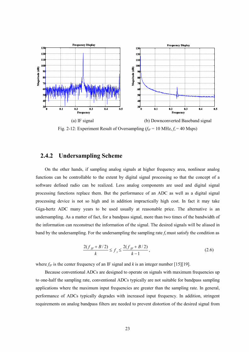
Using the oversampling scheme this system samples the IF signal (centered at 10 MHz) at 40
Msps and then the DDC (Digital Down Conversion) performs the frequency downconversion into
the complex baseband signal. Fig. 2-12 (a) shows the frequency spectrum of sampled IF signal
which is sinusoidal signal of 10.1 MHz assuming centered at fIF = 10 MHz. Fig. 2-12 (b) shows the
frequency spectrum of downconverted baseband signal.
23
0 0.1 0.2 0.3 0.4 0.530
40
50
60
70
80
90
100
110
120
130Frequency Display
Frequency
Mag
nitu
de (d
B)
0 0.1 0.2 0.3 0.4 0.530
40
50
60
70
80
90
100
110
120
130Frequency Display
Frequency
Mag
nitu
de (d
B)
0 0.1 0.2 0.3 0.4 0.5
30
40
50
60
70
80
90
100
110
120
130Frequency Display
Frequency
Mag
nitu
de (d
B)
0 0.1 0.2 0.3 0.4 0.530
40
50
60
70
80
90
100
110
120
130Frequency Display
Frequency
Mag
nitu
de (d
B)
(a) IF signal (b) Downconverted Baseband signal
Fig. 2-12: Experiment Result of Oversampling (fIF = 10 MHz, fs = 40 Msps)
2.4.2 Undersampling Scheme
On the other hands, if sampling analog signals at higher frequency area, nonlinear analog
functions can be controllable to the extent by digital signal processing so that the concept of a
software defined radio can be realized. Less analog components are used and digital signal
processing functions replace them. But the performance of an ADC as well as a digital signal
processing device is not so high and in addition impractically high cost. In fact it may take
Giga-hertz ADC many years to be used usually at reasonable price. The alternative is an
undersampling. As a matter of fact, for a bandpass signal, more than two times of the bandwidth of
the information can reconstruct the information of the signal. The desired signals will be aliased in
band by the undersampling. For the undersampling the sampling rate fs must satisfy the condition as
1)2/(2)2/(2
−+
≤≤+
kBf
fk
Bf IFs
IF , (2.6)
where fIF is the center frequency of an IF signal and k is an integer number [15][19].
Because conventional ADCs are designed to operate on signals with maximum frequencies up
to one-half the sampling rate, conventional ADCs typically are not suitable for bandpass sampling
applications where the maximum input frequencies are greater than the sampling rate. In general,
performance of ADCs typically degrades with increased input frequency. In addition, stringent
requirements on analog bandpass filters are needed to prevent distortion of the desired signal from

24
strong adjacent channel signals. ADCs at low sampling rates are relatively inexpensive and
available and hence this appears promising approach.
Using the undersampling scheme this system samples the IF signal (centered at 70 MHz) at 40
Msps. Fig. 2-13 shows the process of the digital frequency downconversion and the frequency
spectrums. In this figure, the aliasings caused by undersampling appear according to k’s value in
(2.6). The aliasing appearing in-band is the same spectrum of the oversampling. Therefore when
signals digitized by undersampling, the frequency is also downconverted into low-IF
simultaneously. In this system, IF signal centered at 70 MHz is downconverted into low-IF
centered at 10 MHz. The DDC (Digital Down Conversion) performs the frequency
downconversion into baseband in the same manner as the oversampling. Fig. 2-14 (a) shows the
frequency spectrum of sampled IF signal which is sinusoidal signal of 70.1 MHz assuming
centered at fIF = 70 MHz. Fig. 2-14 (b) shows the frequency spectrum of downconverted baseband
signal. In the spectrums of Fig. 2-14 more noise and adverse aliasing caused by a spurious
components appear than when oversampling. Actually when undersampling, stringent requirements
on analog bandpass filters (steep roll-offs) are needed to prevent distortion of the desired signal
from strong adjacent channel signals and hence the filter before ADC must be examined
significantly.
)cos( nc ⋅ω
)sin( nj c ⋅− ω
NCOA/DA/DMixer
LO (8 GHz)
AdaptiveProcessingAdaptiveProcessing
I
Q
Dem
odulationD
emodulation
I
Q
DigitalAnalogDigital Down Converter
BPF
LPF
LPF
LNALNA
BPF Mixer
AMP
LO (380~440 MHz)
8.45 GHz
70 MHz
40 Msps
450 MHz
f c f c2f c f c2
f IF
f c f s f IFf c f s f IF
Fig. 2-13: Frequency Downconversion by Undersampling

25
0 0.1 0.2 0.3 0.4 0.530
40
50
60
70
80
90
100
110
120
130Frequency Display
Frequency
Mag
nitu
de (d
B)
0 0.1 0.2 0.3 0.4 0.530
40
50
60
70
80
90
100
110
120
130Frequency Display
Frequency
Mag
nitu
de (d
B)
0 0.1 0.2 0.3 0.4 0.5
30
40
50
60
70
80
90
100
110
120
130Frequency Display
Frequency
Mag
nitu
de (d
B)
0 0.1 0.2 0.3 0.4 0.530
40
50
60
70
80
90
100
110
120
130Frequency Display
Frequency
Mag
nitu
de (d
B)
(a) IF signal (b) Downconverted Baseband signal
Fig. 2-14: Experiment Result of Undersampling (fIF = 70 MHz, fs = 40 Msps)
2.5 Summary This chapter introduced the digital prototype system for the evaluation of an adaptive antenna.
The architecture was designed based on FPGAs considering IF signal processing and the
reconfigurablity of software defined radio (SDR) and the performance of realtime processing
required to an adaptive antenna system. The architecture of an adaptive antenna system were
discussed and the development processes were described in detail.
26
Chapter 3
Examination of Applications Implementation: MRC Beamforming
Antenna
3.1 Introduction This chapter describes the simple digital phased array antenna using digital beamforming
configuration and introduces its DSP implementation on FPGAs using the prototype system
introduced in Chapter 2. This antenna can steer its main beam toward the DOA (Direction of
Arrival) of incident signal and track automatically. It incorporates MRC (Maximal-Ratio
Combining) beamforming technique that recombines the output power at maximal ratio by
co-phasing received signals at each element like phased array antenna. In this paper, for the sake of
implementation simplicity and use in mobile terminal, it confines only 2 elements. This system
uses FPGAs as digital signal processor to obtain the realtime processing performance of parallel
processing.
3.2 2-Element MRC Beamforming Antenna This paper uses narrowband model for array processing of far-field sources. The incident
wave at k-th element can be represented as
−−⋅= θ
λπ sin)1(2exp)()( dkjnAnxk , for k = 1, 2, (3.1)
where A(n), λ and θ is the envelop, wavelength and DOA angle of an incident wave respectively
and d is the distance spaced between each antenna.
27
After downconversion of the signal (3.1) at each branch, with the complex baseband signal
representations (3.1) at each element can be rewritten as
( )[ ]( )[ ]
( )[ ]φφφ
φ
121mod2
2mod2222
1mod1111
exp)(exp)()(
exp)()(
∆++Φ=
+Φ=+=
+Φ=+=
jna
jnaQjInB
jnaQjInB
, (3.2)
where Φmod is the modulated phase, φ1, φ2 are the phase offset and φ12 is the phase difference
between element 1 and 2. Supposing the receiving power at element 2 is almost same as that of the
element 1 and the difference between them is negligible, the sampled data at element 2 can be
written as
( )
−⋅≈
∆⋅≈
θλπ
φ
sin2exp)(
exp)()(
1
1212
djnB
jnBnB. (3.3)
Generally antenna can steer beam toward intended direction of incident wave by using its steering
vector as the beamforming optimum weight vector. It is certain that beamforming is achieved by
computing the phase difference between elements. The optimum weight can be obtained with only
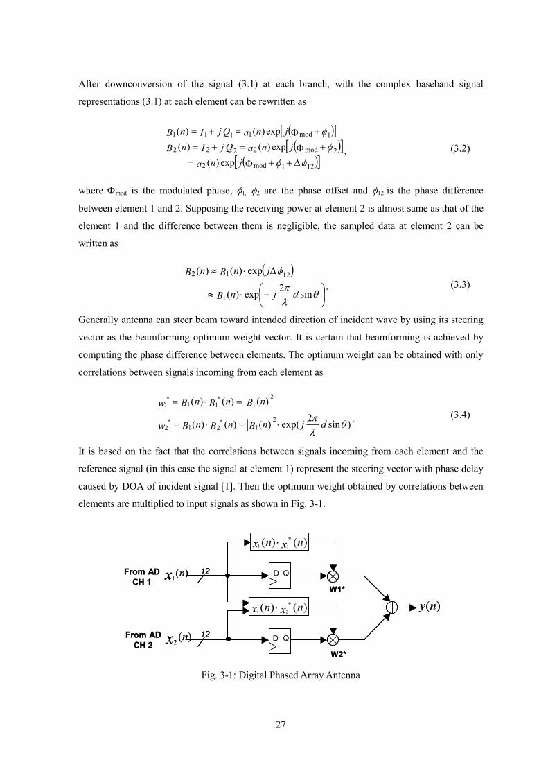
correlations between signals incoming from each element as
)sin2exp()()()(
)()()(
12
212
12
111
θλπ djnBnBnBw
nBnBnBw
⋅=⋅=
=⋅=
∗∗
∗∗
. (3.4)
It is based on the fact that the correlations between signals incoming from each element and the
reference signal (in this case the signal at element 1) represent the steering vector with phase delay
caused by DOA of incident signal [1]. Then the optimum weight obtained by correlations between
elements are multiplied to input signals as shown in Fig. 3-1.
W1*
12
D Q
)()( 21 nxnx ∗⋅
)(1 nx
)(2
nx
)(ny
12
From ADCH 1
From ADCH 2
)()( 11 nxnx ∗⋅
D Q
W2*
W1*
12
D Q
)()( 21 nxnx ∗⋅
)(1 nx
)(2
nx
)(ny
12
From ADCH 1
From ADCH 2
)()( 11 nxnx ∗⋅
D Q
W2* Fig. 3-1: Digital Phased Array Antenna
28
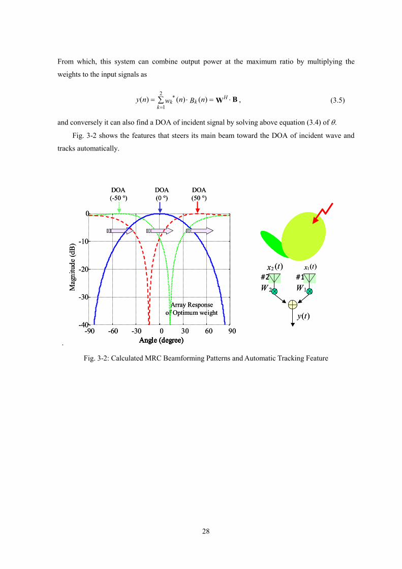
From which, this system can combine output power at the maximum ratio by multiplying the
weights to the input signals as
BW ⋅=⋅= ∑=
∗ Hk
kk nBnwny )()()(
2
1, (3.5)
and conversely it can also find a DOA of incident signal by solving above equation (3.4) of θ.
Fig. 3-2 shows the features that steers its main beam toward the DOA of incident wave and
tracks automatically.
.
Array Responseof Optimum weight
-90 -60 -30 0 30 60 90-40
-30
-20
-10
0
Angle (degree)
Mag
nitu
de (d
B)
DOA(-50 °)
Angle (degree)
DOA(0 °)
Angle (degree)
DOA(50 °)
Array Responseof Optimum weight
-90 -60 -30 0 30 60 90-40
-30
-20
-10
0
Angle (degree)
Mag
nitu
de (d
B)
DOA(-50 °)
Angle (degree)
DOA(0 °)
Angle (degree)
DOA(50 °)
#1#2
)(1 tx)(2 tx
W 2 W1
)(ty
#1#2
)(1 tx)(2 tx
W 2 W1
)(ty
Fig. 3-2: Calculated MRC Beamforming Patterns and Automatic Tracking Feature
29
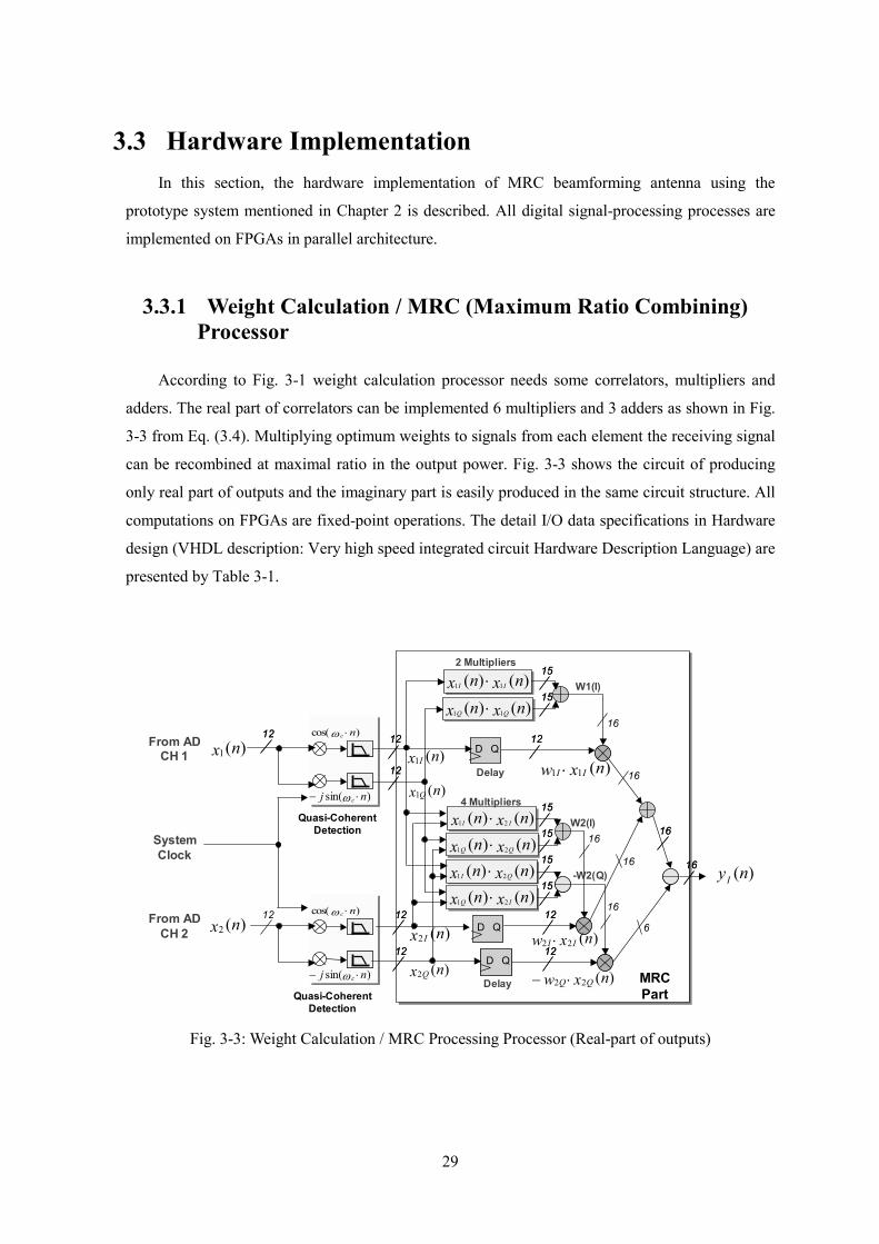
3.3 Hardware Implementation In this section, the hardware implementation of MRC beamforming antenna using the
prototype system mentioned in Chapter 2 is described. All digital signal-processing processes are
implemented on FPGAs in parallel architecture.
3.3.1 Weight Calculation / MRC (Maximum Ratio Combining) Processor
According to Fig. 3-1 weight calculation processor needs some correlators, multipliers and
adders. The real part of correlators can be implemented 6 multipliers and 3 adders as shown in Fig.
3-3 from Eq. (3.4). Multiplying optimum weights to signals from each element the receiving signal
can be recombined at maximal ratio in the output power. Fig. 3-3 shows the circuit of producing
only real part of outputs and the imaginary part is easily produced in the same circuit structure. All
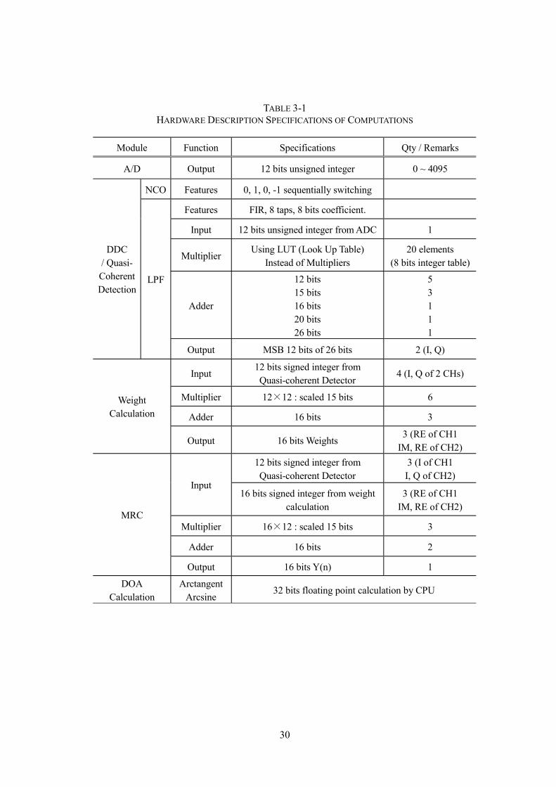
computations on FPGAs are fixed-point operations. The detail I/O data specifications in Hardware
design (VHDL description: Very high speed integrated circuit Hardware Description Language) are
presented by Table 3-1.
)cos( nc ⋅ω
)sin( nj c ⋅− ω
)cos( nc ⋅ω
)sin( nj c ⋅− ω
)cos( nc ⋅ω
)sin( nj c ⋅− ω
)cos( nc ⋅ω
)sin( nj c ⋅− ω
W1(I)
W2(I)
)(nyI
)()( 21 nxnx QQ ⋅
)()( 21 nxnx II ⋅
)(1 nx I
)(1 nx Q
)(2 nx I
)(2 nx Q
)()( 21 nxnx IQ ⋅
)()( 21 nxnx QI ⋅
Delay
)(1 nx
)(2 nx
From ADCH 1
From ADCH 2
)()( 11 nxnx QQ ⋅
Delay
)()( 11 nxnx II ⋅
-W2(Q)
2 Multipliers
4 Multipliers
)(11 nxw II ⋅
)(22 nxw QQ ⋅−
)(22 nxw II ⋅
D QD Q
D QD Q
D QD Q
1212
12
1212
1212
1212
1212
1212
1515
1515
1515
1515
1515
1515
1212
1212
16
16
16
1616
1616
6
16
16
Quasi-CoherentDetection
SystemClock
MRCPartQuasi-Coherent
Detection Fig. 3-3: Weight Calculation / MRC Processing Processor (Real-part of outputs)
30
TABLE 3-1 HARDWARE DESCRIPTION SPECIFICATIONS OF COMPUTATIONS
Module Function Specifications Qty / Remarks
A/D Output 12 bits unsigned integer 0 ~ 4095
NCO Features 0, 1, 0, -1 sequentially switching
Features FIR, 8 taps, 8 bits coefficient.
Input 12 bits unsigned integer from ADC 1
Multiplier Using LUT (Look Up Table)
Instead of Multipliers 20 elements
(8 bits integer table)
Adder
12 bits 15 bits 16 bits 20 bits 26 bits
5 3 1 1 1
DDC / Quasi- Coherent Detection
LPF
Output MSB 12 bits of 26 bits 2 (I, Q)
Input 12 bits signed integer from Quasi-coherent Detector
4 (I, Q of 2 CHs)
Multiplier 12×12 : scaled 15 bits 6
Adder 16 bits 3
Weight Calculation
Output 16 bits Weights 3 (RE of CH1
IM, RE of CH2) 12 bits signed integer from Quasi-coherent Detector
3 (I of CH1 I, Q of CH2)
Input 16 bits signed integer from weight
calculation 3 (RE of CH1
IM, RE of CH2)
Multiplier 16×12 : scaled 15 bits 3
Adder 16 bits 2
MRC
Output 16 bits Y(n) 1
DOA Calculation
Arctangent Arcsine
32 bits floating point calculation by CPU
31
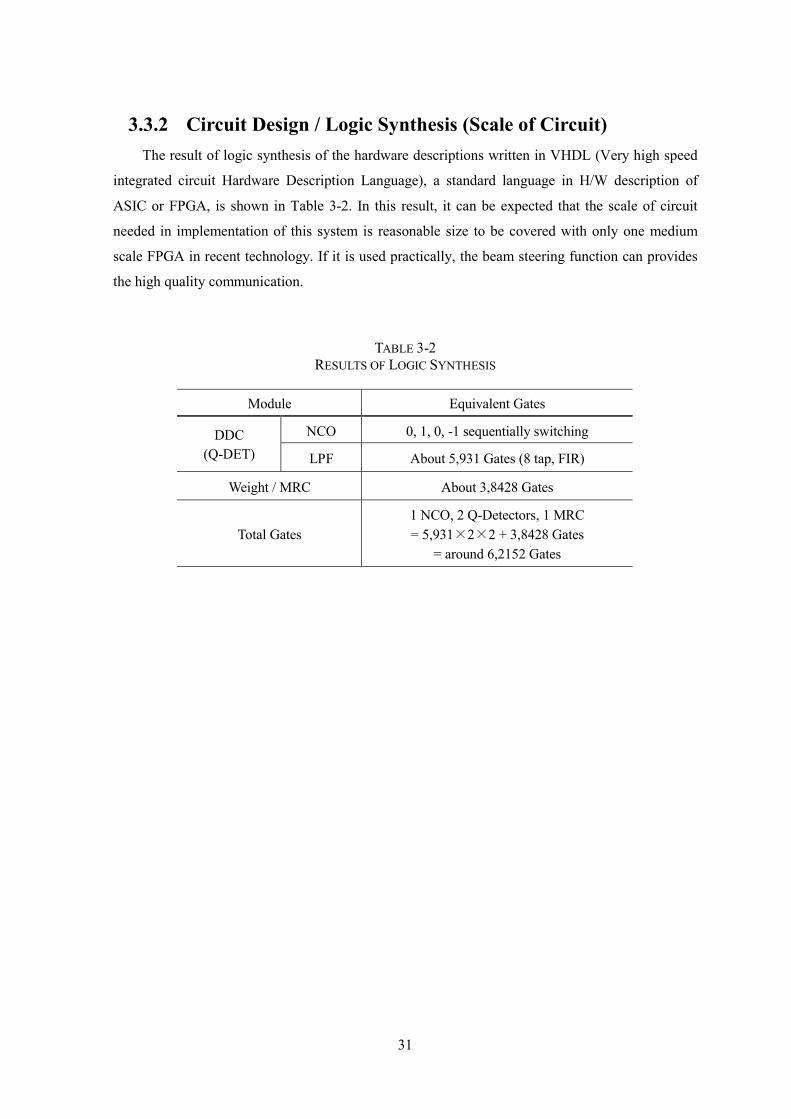
3.3.2 Circuit Design / Logic Synthesis (Scale of Circuit)
The result of logic synthesis of the hardware descriptions written in VHDL (Very high speed
integrated circuit Hardware Description Language), a standard language in H/W description of
ASIC or FPGA, is shown in Table 3-2. In this result, it can be expected that the scale of circuit
needed in implementation of this system is reasonable size to be covered with only one medium
scale FPGA in recent technology. If it is used practically, the beam steering function can provides
the high quality communication.
TABLE 3-2 RESULTS OF LOGIC SYNTHESIS
Module Equivalent Gates
NCO 0, 1, 0, -1 sequentially switching DDC (Q-DET) LPF About 5,931 Gates (8 tap, FIR)
Weight / MRC About 3,8428 Gates
Total Gates 1 NCO, 2 Q-Detectors, 1 MRC = 5,931×2×2 + 3,8428 Gates
= around 6,2152 Gates

32
3.4 Experimental Results This section introduces the experimental results. This experiment is DOA estimation with
obtained optimum weight. MRC beamforming function steers beam toward DOA of incident
signal. Conversely the DOA angle can be obtained from the MRC optimum weight.
From (3.4) the phase difference Θ between signals can be obtained by the arctangent of the
imaginary part to real part ratio of optimum weight.
==Θ
∗
∗−
)Re()Im(2
2
21tansinwwd θ
λπ
(3.6)
And the DOA θ can also computed by solving as
⋅ ∗
∗−−=
)Re()Im(
2
211 tan2sinww
dπλ
θ . (3.7)
From (3.7) the DOA of incident signal can be found by MRC optimum weight because MRC steers
the main beam toward the direction of incident wave. This operation confirms the beamsteering
function of MRC processor.
The experimental configuration is shown as Fig. 3-4. Experiments were performed in a radio
anechoic chamber to validate the functionality of the design. Array antennas of 2 elements are
omni-directional and spaced by λ/2 between each other. The RF frequency is 8.45 GHz and
received RF signals are downconverted into IF (1 MHz) in the RF receiver. Sampling rates and
resolution of ADCs is 4 MHz and 12 bits respectively. This experiment was performed supposing
that there is only 1 incident wave and decimation factor is 1. All digital signal processing stages
such as DDC, weight calculation and maximal ratio combining are performed on FPGAs. The
detail experimental parameters are illustrated in Table 3-3.

33
λ/2
λ/4λ/4
λ/2
λ/4λ/4
Receiver
Transmitter
Anechoic Chamber
MRC Processing
Fig. 3-4: Experimental Configuration
TABLE 3-3 EXPERIMENTAL PARAMETERS
Antennas 2 elements spaced by λ/2
RF Frequency 8.45 GHz
RF D/C Analog down-conversion
by Receiver
IF Frequency 1 MHz
IF D/C Digital Down-Conversion
Sampling Rates 4 MHz (×4 Oversampling)
Detection method Quasi-Coherent Detection
Baseband Freq. 25 KHz
Modulation CW (unmodulated signal)
34
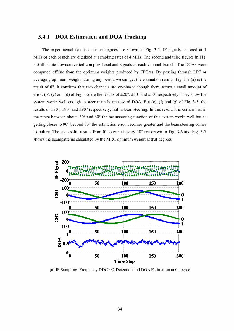
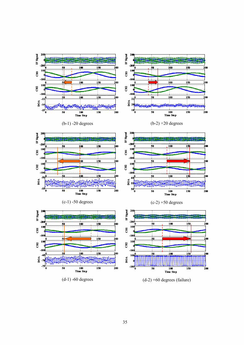
3.4.1 DOA Estimation and DOA Tracking
The experimental results at some degrees are shown in Fig. 3-5. IF signals centered at 1
MHz of each branch are digitized at sampling rates of 4 MHz. The second and third figures in Fig.
3-5 illustrate downconverted complex baseband signals at each channel branch. The DOAs were
computed offline from the optimum weights produced by FPGAs. By passing through LPF or
averaging optimum weights during any period we can get the estimation results. Fig. 3-5 (a) is the
result of 0°. It confirms that two channels are co-phased though there seems a small amount of
error. (b), (c) and (d) of Fig. 3-5 are the results of ±20°, ±50° and ±60° respectively. They show the
system works well enough to steer main beam toward DOA. But (e), (f) and (g) of Fig. 3-5, the
results of ±70°, ±80° and ±90° respectively, fail in beamsteering. In this result, it is certain that in
the range between about -60° and 60° the beamsteering function of this system works well but as
getting closer to 90° beyond 60° the estimation error becomes greater and the beamsteering comes
to failure. The successful results from 0° to 60° at every 10° are drawn in Fig. 3-6 and Fig. 3-7
shows the beampatterns calculated by the MRC optimum weight at that degrees.
0 50 100 150 200-200
0
200
IF S
igna
l
0 50 100 150 200-100
0100
CH
1
0 50 100 150 200-100
0100
CH
2
0 50 100 150 2000
0.5
1
Time Step
DO
A
0 50 100 150 200-200
0
200
0 50 100 150 200-200
0
200
IF S
igna
l
0 50 100 150 200-100
0100
CH
1
0 50 100 150 200-100
0100
CH
2
0 50 100 150 2000
0.5
1
Time Step
DO
A
QI
QI
0 50 100 150 200-200
0
200
IF S
igna
l
0 50 100 150 200-100
0100
CH
1
0 50 100 150 200-100
0100
CH
2
0 50 100 150 2000
0.5
1
Time Step
DO
A
0 50 100 150 200-200
0
200
0 50 100 150 200-200
0
200
IF S
igna
l
0 50 100 150 200-100
0100
CH
1
0 50 100 150 200-100
0100
CH
2
0 50 100 150 2000
0.5
1
Time Step
DO
A
QI
QI
(a) IF Sampling, Frequency DDC / Q-Detection and DOA Estimation at 0 degree
35
0 50 100 150 200-200
0
200
IF S
igna
l
0 50 100 150 200-100
0100
CH
1
0 50 100 150 200-100
0100
CH
2
0 50 100 150 200-15
-14
-13
Time Step
DO
A
0 50 100 150 200-200
0
200
0 50 100 150 200-200
0
200
IF S
igna
l
0 50 100 150 200-100
0100
CH
1
0 50 100 150 200-100
0100
CH
2
0 50 100 150 200-15
-14
-13
Time Step
DO
A
(b-1) -20 degrees
0 50 100 150 200-200
0
200
IF S
igna
l
0 50 100 150 200-100
0100
CH
1
0 50 100 150 200-100
0100
CH
2
0 50 100 150 20018
20
22
Time Step
DO
A
0 50 100 150 200-200
0
200
0 50 100 150 200-200
0
200
IF S
igna
l
0 50 100 150 200-100
0100
CH
1
0 50 100 150 200-100
0100
CH
2
0 50 100 150 20018
20
22
Time Step
DO
A
(b-2) +20 degrees
0 50 100 150 200-200
0
200
IF S
igna
l
0 50 100 150 200-100
0100
CH
1
0 50 100 150 200-100
0100
CH
2
0 50 100 150 200-55
-50
Time Step
DO
A
0 50 100 150 200-200
0
200
0 50 100 150 200-200
0
200
IF S
igna
l
0 50 100 150 200-100
0100
CH
1
0 50 100 150 200-100
0100
CH
2
0 50 100 150 200-55
-50
Time Step
DO
A
(c-1) -50 degrees
0 50 100 150 200-200
0
200
IF S
igna
l
0 50 100 150 200-100
0100
CH
1
0 50 100 150 200-100
0100
CH
2
0 50 100 150 20050
55
60
Time Step
DO
A
0 50 100 150 200-200
0
200
0 50 100 150 200-200
0
200
IF S
igna
l
0 50 100 150 200-100
0100
CH
1
0 50 100 150 200-100
0100
CH
2
0 50 100 150 20050
55
60
Time Step
DO
A
(c-2) +50 degrees
0 50 100 150 200-200
0
200
IF S
igna
l
0 50 100 150 200-100
0100
CH
1
0 50 100 150 200-100
0100
CH
2
0 50 100 150 200-75
-70
-65
Time Step
DO
A
0 50 100 150 200-200
0
200
0 50 100 150 200-200
0
200
IF S
igna
l
0 50 100 150 200-100
0100
CH
1
0 50 100 150 200-100
0100
CH
2
0 50 100 150 200-75
-70
-65
Time Step
DO
A
(d-1) -60 degrees
0 50 100 150 200-200
0
200
IF S
igna
l
0 50 100 150 200-100
0100
CH
1
0 50 100 150 200-100
0100
CH
2
0 50 100 150 200-100
0
100
Time Step
DO
A
0 50 100 150 200-200
0
200
IF S
igna
l
0 50 100 150 200-100
0100
CH
1
0 50 100 150 200-100
0100
CH
2
0 50 100 150 200-100
0
100
Time Step
DO
A
(d-2) +60 degrees (failure)

36
0 50 100 150 200-200
0
200
IF S
igna
l
0 50 100 150 200-100
0100
CH
1
0 50 100 150 200-100
0100
CH
2
0 50 100 150 200-80
-70
-60
Time Step
DO
A
0 50 100 150 200-200
0
200
IF S
igna
l
0 50 100 150 200-100
0100
CH
1
0 50 100 150 200-100
0100
CH
2
0 50 100 150 200-80
-70
-60
Time Step
DO
A
(e-1) -70 degrees
0 50 100 150 200-200
0
200
IF S
igna
l
0 50 100 150 200-100
0100
CH
1
0 50 100 150 200-100
0100
CH
2
0 50 100 150 200-100
0
100
Time Step
DO
A
0 50 100 150 200-200
0
200
IF S
igna
l
0 50 100 150 200-100
0100
CH
1
0 50 100 150 200-100
0100
CH
2
0 50 100 150 200-100
0
100
Time Step
DO
A(e-2) +70 degrees (failure)
0 50 100 150 200-200
0
200
IF S
igna
l
0 50 100 150 200-100
0100
CH
1
0 50 100 150 200-100
0100
CH
2
0 50 100 150 20065
70
75
Time Step
DO
A
0 50 100 150 200-200
0
200
IF S
igna
l
0 50 100 150 200-100
0100
CH
1
0 50 100 150 200-100
0100
CH
2
0 50 100 150 20065
70
75
Time Step
DO
A
(f-1) -80 degrees (failure)
0 50 100 150 200-200
0
200
IF S
igna
l
0 50 100 150 200-100
0100
CH
1
0 50 100 150 200-100
0100
CH
2
0 50 100 150 200-65
-60
-55
Time Step
DO
A
0 50 100 150 200-200
0
200
IF S
igna
l
0 50 100 150 200-100
0100
CH
1
0 50 100 150 200-100
0100
CH
2
0 50 100 150 200-65
-60
-55
Time Step
DO
A
0 50 100 150 200-200
0
200
IF S
igna
l
0 50 100 150 200-100
0100
CH
1
0 50 100 150 200-100
0100
CH
2
0 50 100 150 200-65
-60
-55
Time Step
DO
A
(f-2) +80 degrees (failure)
0 50 100 150 200-200
0
200
IF S
igna
l
0 50 100 150 200-100
0100
CH
1
0 50 100 150 200-100
0100
CH
2
0 50 100 150 20065
70
75
Time Step
DO
A
0 50 100 150 200-200
0
200
IF S
igna
l
0 50 100 150 200-100
0100
CH
1
0 50 100 150 200-100
0100
CH
2
0 50 100 150 20065
70
75
Time Step
DO
A
(g-1) -90 degrees (failure)
0 50 100 150 200-200
0
200
IF S
igna
l
0 50 100 150 200-100
0100
CH
1
0 50 100 150 200-100
0100
CH
2
0 50 100 150 200-60
-55
-50
Time Step
DO
A
0 50 100 150 200-200
0
200
IF S
igna
l
0 50 100 150 200-100
0100
CH
1
0 50 100 150 200-100
0100
CH
2
0 50 100 150 200-60
-55
-50
Time Step
DO
A
(g-2) +90 degrees (failure)
Fig. 3-5: IF Sampling, Frequency DDC / Q-Detection and DOA Estimation

37
0 10 20 30 40 50
-80
-60
-40
-20
0
20
40
60
80
DOA ESTIMATION
Time Step
DO
A50 deg.
40 deg
30 deg
20 deg
10 deg
0 deg
-10 deg -20 deg
-30 deg
-40 deg
-50 deg
-60 deg
Fig. 3-6: DOA Estimation Results at every 10°
-90 -60 -30 0 30 60 90-30
-25
-20
-15
-10
-5
0
Angle (degree)
Mag
nitude
(dB
)
-90 -60 -30 0 30 60 90-30
-25
-20
-15
-10
-5
0
Angle (degree)
Mag
nitude
(dB
)
Fig. 3-7: Beampattern formed by MRC optimum weight when the DOA is at every 10°

38
This system can track automatically sample by sample in realtime. Fig. 3-8 shows well arcsine
curve characteristic despite moving at linear speed due to the fact that DOA is the arcsine function
of phase difference between signals from (3.6),(3.7). Exceeding ±60° the estimation values
become unstable because the phase difference between signals becomes to greater than λ/2 and
computation results are unbelievable in the vicinity of 60°.
0 0.5 1 1.5 2 2.5 3 3.5 4x 10
6
-80
-60
-40
-20
0
20
40
60
80
DOA ESTIMATION
Time Step
DOA
(θ)
--9900°° +9+900°°
0 0.5 1 1.5 2 2.5 3 3.5 4x 10
6
-80
-60
-40
-20
0
20
40
60
80
DOA ESTIMATION
Time Step
DOA
(θ)
--9900°° +9+900°°
Fig. 3-8: DOA Tracking Feature (moving linearly from -90° to 90°)
3.4.2 Discussion
According to the previous subsections, only in the range of DOA between -60° and +60° the
beamsteering function of the system operates well. The error of the phase difference between
signals becomes larger causes the unbelievable results. There may be many error factors. Fig. 3-9
shows an antenna placement error. If used high frequency, this error is very critical. For more
accurate in wider range of DOA, the change of antenna pattern caused by mutual coupling must be
also considered. And actually antennas have not ideal omni-directional radiation pattern and are not
identical. Therefore the compensation of errors must be taken into account.
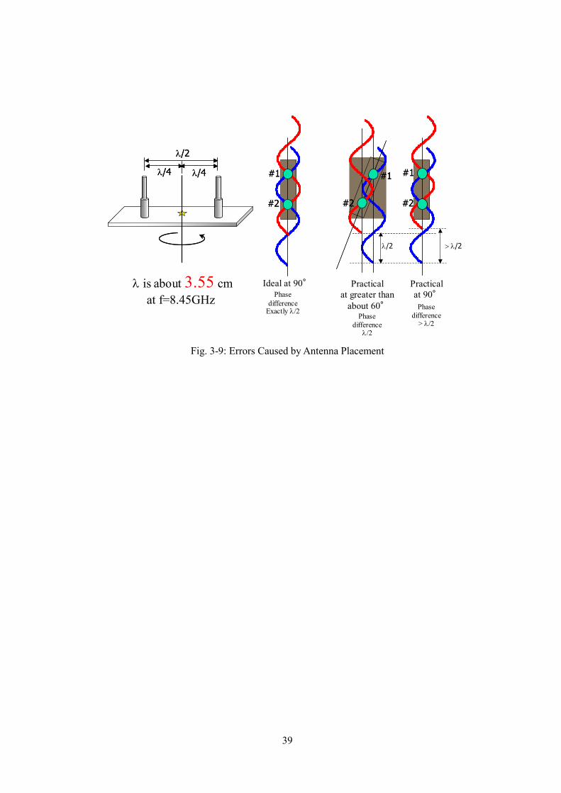
39
λ/2
λ/4λ/4
λ/2
λ/4λ/4
#2
#1
#2
#1
#2
#1
#2
#1
#2
#1
#2
#1
Ideal at 90° Practical at greater than
about 60°
Practical at 90°Phase
difference Exactly λ/2
Phase difference
λ/2
Phase difference
> λ/2
λ is about 3.55 cmat f=8.45GHz
λ/2 > λ/2
Fig. 3-9: Errors Caused by Antenna Placement

40
3.5 Examination of Digital Calibration of Array Antenna Generally there are many error factors of use adaptive antenna array in actual field such as
antenna placement error, mutual coupling, nonlinearity of RF devices and etc. To use adaptive
array antenna system in actual field, the basic calibration or compensation stages or processes must
be required. First of all, the fact that antenna pattern is not ideal and distorts the amplitude and
phase of input signal. Generally, this antenna response is a function of DOA angle and each
antenna has a different radiation pattern. So the complete calibration requires the information of
antenna manifold in advance and needs an additional huge circuitry. Digital approach has many
advantages over the calibration using nonlinear analog devices dominated by the environment like
temperature.
This section introduces digital approaches to calibration of array receiver. They operate not for
all DOAs but the only initial calibration at specified DOA between elements. They play a role in
the adjustment to a desired phase and amplitude between signals at any antenna elements. This
section proposes two useful digital signal processing techniques easy to implement on an FPGA.
One is the adjustment by control of the amplitude and the phase of an NCO (Numerical Controlled
Oscillator) that act as mixer in analog sense. The other is using MRC (Maximum Ratio Combining)
optimum weight. In this chapter, the basic ideas and a few advantages / disadvantages of the two
techniques are described.
3.5.1 Adjustment by NCO Control
The complex baseband signal is obtained by lowpass filtering IF (Intermediate Frequency)
signal mixed with or multiplied by NCO as mentioned in section 2.3.2 of Chapter 2. The signal
)(~ nx multiplied by NCO is given by
eMnxnx nj⋅⋅= ⋅− ω)()(~ , (3.8)
where )(nx is an IF signal, M and ω are an amplitude and frequency of NCO respectively.
Generally in DDC (Digital Down Conversion) stage, NCO frequency ω is ωc. From (3.8) it is
certain that by using phase shifter and gain controller to NCO at IF DDC stage the phase and
amplitude of each signal can be adjusted. Assuming the amplitude of NCO M is 1 in (3.8), the
adjusted frequency shifted signal can be obtained by (3.9).
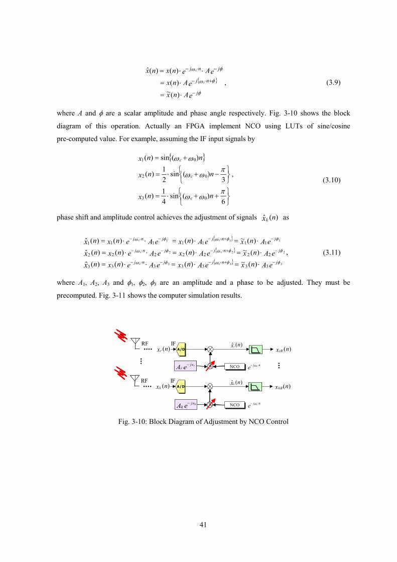
41
{ }
eAnxeAnx
eAenxnx
j
nj
jnj
c
c
φ
φω
φω
−
+⋅−
−⋅−
⋅=
⋅=
⋅⋅=
)(~)(
)()(ˆ
, (3.9)
where A and φ are a scalar amplitude and phase angle respectively. Fig. 3-10 shows the block
diagram of this operation. Actually an FPGA implement NCO using LUTs of sine/cosine
pre-computed value. For example, assuming the IF input signals by
{ }
++⋅=
−+⋅=
+=
6)(sin
41)(
3)(sin
21)(
)(sin)(
03
02
01
πωω
πωω
ωω
nnx
nnx
nnx
c
c
c
, (3.10)
phase shift and amplitude control achieves the adjustment of signals )(ˆ nxk as
{ }
{ }
{ } eAnxeAnxeAenxneAnxeAnxeAenxn
eAnxeAnxeAenxn
jnjjnj
jnjjnj
jnjjnj
cc
cc
cc
xxx
φφωφω
φφωφω
φφωφω
333
222
111
3333333
2222222
1111111
)(~)()()()(~)()()(
)(~)()()(
ˆˆˆ
−+⋅−−⋅−
−+⋅−−⋅−
−+⋅−−⋅−
⋅=⋅=⋅⋅=
⋅=⋅=⋅⋅=
⋅=⋅=⋅⋅=
, (3.11)
where A1, A2, A3 and φ1, φ2, φ3 are an amplitude and a phase to be adjusted. They must be
precomputed. Fig. 3-11 shows the computer simulation results.
A/DA/DIF
)(nxr
RF )(ˆ nxr )(nxrB
e nj c⋅− ωNCONCO
A/DA/DIF
)(nxk
RF )(ˆ nxk )(nxkB
e nj c⋅− ωNCONCO
eA kjk
φ−
eA rjr
φ−
eA kjk
φ−
eA rjr
φ−
Fig. 3-10: Block Diagram of Adjustment by NCO Control

42
{ }
++⋅=
−+⋅=
+=
6)(sin
41)(
3)(sin
21)(
)(sin)(
03
02
01
π
π
nwwnx
nwwnx
nwwnx
c
c
c
0 5 10 15 20 25 30 35 40-2000
0
2000
0 5 10 15 20 25 30 35 40-2000
0
2000
0 5 10 15 20 25 30 35 40-2000
0
2000
-1500 -1000 -500 0 500 1000 1500-1500
-1000
-500
0
500
1000
1500
Time Display IF Signal x1, x2, x3Adjusted & Detected x1, x2, x3
Mapping of x1i-x1i, x1i-x2i, x1i-x3i
0 50 100 150 200 250 300-2000
0
2000
0 50 100 150 200 250 300-2000
0
2000
0 50 100 150 200 250 300-2000
0
2000
Adjusted NCO for x1, x2, x3
0 5 10 15 20 25 30 35 40-4
-2
0
2
4
0 5 10 15 20 25 30 35 40-4
-2
0
2
4
0 5 10 15 20 25 30 35 40-4
-2
0
2
4
6,
3,0
4,2,1
321
321
33
22
11
3
2
1
πφ
πφφ
φ
φ
φ
ω
ω
ω
=−==
===⋅=
⋅=
⋅=
−⋅−
−⋅−
−⋅−
AAAeAeNCOeAeNCOeAeNCO
jnj
jnj
jnj
c
c
c
IQI
QI
QI
Q
Fig. 3-11: Computer Simulation Result of Adjustment by NCO Control
3.5.2 Adjustment by Maximal Ratio Combining (MRC)
If uses narrowband model for array processing of far-field sources as described in previous
sections of this chapter, the baseband signals at r-th element as a reference signal and at k-th
element can be represented as
eBensnx
eAnsnxjdj
kB
jrB
)(sin2
)(
)()()(
)()()(θζθ
λπ
θφ
θ
θ
−−
−
⋅⋅=
⋅=, (3.12)
where s(n) is the baseband complex temporal amplitude, A(θ), B(θ) and φ(θ), ζ(θ) are scalar
amplitudes and phase angles respectively which are an antenna response function of θ. λ and θ
are the wavelength and the DOA of an incident signal respectively and d is the distance spaced
between elements. The MRC optimum weight can be obtained with correlations between signals
coming from each element as
{ }eBAensnxnxr
Bnsnxnxr
Ansnxnxr
jdjkBrBrk
kBkBkk
rBrBrr
)()(sin22
2
2
)()()()()(
)()()()(
)()()()(
θζθφθλπ
θθ
θ
θ
−−∗∗
∗∗
∗∗
⋅⋅⋅=⋅=
⋅=⋅=
⋅=⋅=
, (3.13)
The MRC optimum weight adjusts the baseband signals to the same amplitude and phase by (3.14)
with one another. (3.14) can be applied if the receiving powers of input signals has not the same
level by multiplying the scaling factor with each other, which is different from (3.4).

43
)()()()()()(
nxwnxrrnx
nxwnxrrnx
k kBkBrrrkkB
rBrrBkkrrrB
⋅=⋅⋅=′⋅=⋅⋅=′
∗∗∗
∗∗∗
, (3.14)
(3.14) needs only multiply operations, and hence it is easy to implement on an FPGA. It can be
incorporated in pre-stage of adaptive signal processing as a vector rotation adjustment process as
shown in Fig. 3-12. This calibration process must already know the exact DOA of transmitting
calibration signal and it can be the simplest case that the DOA is 0°. Once this initializing process
is performed, the resulting rotation vectors are stored in memory (in FPGAs) and are used from the
next operation steps.
A/DA/DIF
)(nxr
RF )(~ nx r
A/DA/DIF
)(nxk
RF )(~ nxk
e nj c⋅− ωNCONCO
)(nxrB
)(nxkB
Vector RotationWith MRC WeightVector Rotation
With MRC Weight
)(nxrB
)(nxkB
Vector RotationWith MRC WeightVector Rotation
With MRC Weight
Next Stage
Next Stage
Fig. 3-12: Block Diagram of Adjustment by using MRC weight
0 5 10 15 20 25 30 35 40-2000
0
2000
0 5 10 15 20 25 30 35 40-2000
0
2000
0 5 10 15 20 25 30 35 40-2000
0
2000
0 50 100 150 200 250 300-2000
0
2000
0 50 100 150 200 250 300-2000
0
2000
0 50 100 150 200 250 300-2000
0
2000
-1500 -1000 -500 0 500 1000 1500-1500
-1000
-500
0
500
1000
1500
Time Display IF Signal x1, x2, x3Adjusted x1, x2, x3
Mapping of x1i-x1i, x1i-x2i, x1i-x3i
{ }
++⋅=
−+⋅=
+=
6)(sin
41)(
3)(sin
21)(
)(sin)(
03
02
01
π
π
nwwnx
nwwnx
nwwnx
c
c
c
0 50 100 150 200 250 300-2000
0
2000
0 50 100 150 200 250 300-2000
0
2000
0 50 100 150 200 250 300-2000
0
2000
-1500 -1000 -500 0 500 1000 1500-1500
-1000
-500
0
500
1000
1500
Detected x1, x2, x3
Mapping of x1i-x1i, x1i-x2i, x1i-x3i
0 50 100 150 200 250 300-2000
0
2000
0 50 100 150 200 250 300-2000
0
2000
0 50 100 150 200 250 300-2000
0
2000
-1500 -1000 -500 0 500 1000 1500-1500
-1000
-500
0
500
1000
1500
Detected x1, x2, x3
Mapping of x1i-x1i, x1i-x2i, x1i-x3i
IQI
QI
QI
QI
QI
QI
QI
Q
Fig. 3-13: Computer Simulation Result of Adjustment by NCO Control

44
3.5.3 Discussion
In this section, two digital calibration techniques were examined. The adjustment by NCO
control is performed at IF stage. In this technique, an additional vector rotation circuit is not needed
but the control values of NCO to adjust must be already known by any other computation process.
In addition adjustment accuracy is dependent on a resolution of NCO sine/cosine table, that is, a
large size of LUT is taken for an exact adjustment. On the other hand, the adjustment using the
MRC optimum weight is performed at baseband. And additional vector rotation circuit is required
but phase adjustment accuracy is relatively higher because it is indifferent to resolution of any table
values stored in memory. The adjustment using MRC optimum weight is suitable for an FPGA
implementation thanks to the simplicity.
3.6 Summary In this chapter, the implementation of a simple digital phased array antenna using digital
beamforming network was examined especially by using FPGAs as a DSP processor. It can steer a
beam toward DOA of an incident signal automatically. This beamsteering function will provide
more effective communication performance than fixed beam antenna. The circuit in FPGAs was
implemented in simple parallel structure and the performance is expected to meet the requirement
of realtime processing in practical wireless communications. The circuit has reasonable scale and
can be expected to implement at low price. By some experiment in a radio anechoic chamber, the
functionalities such as beamforming and DOA tracking are validated. This system can operate well
in the range between -60° and +60° without any compensation or calibration. Finally, the digital
approach to calibration of antenna response was introduced. For the present, it uses only for
initialising the antenna response at any specific DOA.

45
Chapter 4
Examination of Applications Implementation: DOA Estimation By
MUSIC Method
4.1 Introduction Chapter 3 presented a beamforming application by an MRC beamforming antenna. That can
steer and track automatically toward only one desired signal by using correlation between signals
incoming at each element. Suppose that an adaptive antenna is only employed at the base station
and not the mobile station, the mobile stations transmit using omni-directional antennas and
therefore base-stations must employ spatially selective reception in order to separate the desired
signals from interferences. As a matter of fact, when receiving communication signals at an
adaptive antenna array, it is indispensable to estimate DOAs of incident signals and uses the DOAs
in a beamformer in order to separate the desired signal. In this chapter the implementation issues in
MUSIC (MUltiple SIgnal Classification) method, which is one of super resolution DOA estimation
methods, and an examination of hardware design to implement on FPGAs are mentioned.
MUSIC is a subspace-based method. All the subspace-based methods are based on the EVD
of the covariance (or correlation) matrix and the EVD is very difficult to process in realtime
because of its heavy computational load and complexity. Section 4.5 describes the design of an
EVD processor suitable for realtime processing hardware implementation. The architecture uses
Cyclic Jacobi method based on CORDIC (COordinate Rotation DIgital Computer).

46
4.2 Performance Requirement As mentioned before, in the communication environment multi-path fading caused by a
reflection by any physical structures is a very serious problem. When passing through multi-path,
the signals are delayed and out of phase from the signals through direct-path that causes the signal
strength to be changed extremely at a receiver end and hence receiving quality is also reduced as
shown in Fig. 4-1. The requirement of wider band and higher transmission rate in the next
generation communications makes it more critical, furthermore when the mobile terminal moves at
high speed the transmission rate may be confined by this problem. If can solve the multi-path
fading, the trade off between mobility and transmission rate will be dramatically improved.
Adaptive antenna technologies can provide a solution of multi-path fading. The adaptive
antenna can suppress the adverse effect of multi-path delayed coherent signals and interferences by
steering beams toward intended direction and nulls the other undesired directions so that it can
achieve high communication quality. This operation makes the receiving signal strength flat and
stable over a threshold level. Therefore an adaptive antenna must find the DOAs of signals and
form beams and nulls within a fading pitch. Considering mobility of several hundreds of km/s, the
fading pitch becomes very short time, several µs. It is very difficult to compute them by a general
serial structure DSP processor, and hence the high-speed parallel computations with a specific
processor must be needed.
Non-Fade Period
FadeFadeFade
SignalAmplitude
Time
Threshold level
Non-Fade Period
FadeFadeFade
SignalAmplitude
Time
Threshold level
Fig. 4-1: Change of Received Signal Amplitude Under Multi Path Fading Environment

47
4.3 DOA Estimation using MUSIC Method MUSIC (MUltiple SIgnal Classification) method is a kind of DOA (Direction Of Arrival)
estimation algorithm based on eigenvector decomposition, which is also called based on spatial
structure method. It has the capability to estimate DOA in much higher resolution than other
conventional methods.
Spatial structure methods like MUSIC exploit the information in the steering vector a(θ). The
model of a signal X(t) received at K array elements are linear combinations of the L incident
signals and noise. In this case, the steering vector is written by
−−−= )sin2exp()sin2exp()sin2exp()( 21 θ
λπ
θλπ
θλπ
θ iKii
T
i djdjdj …a , (4.1)
and matrix expression of X(t) is as following.
)()()(
)()()()(1
tt
ttFtL
ll
NFA
NaX
+=
∑ +⋅==
θ
θ (4.2)
where N(t) is a noise vector and A(θ) and F(t) are defined as (4.3) respectively.
[ ][ ])()()()(
)()()()(
21
21
tFtFtFt LT
L
…
…
=
=
F
aaaA θθθθ (4.3)
The correlation matrix of X(t) is obtained by
[ ])()( ttE HXX XXR = (4.4)
(4.4) can be rewritten by substituting (4.2)
[ ] [ ])()()()( ttEttE HHHXX NNASSAR +⋅⋅= (4.5)
The correlation matrix of S(t) is denoted by RSS and assuming N(t) is a White Gausian noise, the
correlation matrix of N(t) is σ2I. Therefore RXX can be written as
IARAR σ 2+⋅⋅= HSSXX (4.6)
Since RXX is a positive definite hermitian matrix, the correlation matrix of x(t) can be decomposed
by EVD(Eigen Value Decomposition) as
48
UUR HXX ⋅⋅= Λ . (4.7)
where U is an unitary matrix composed of eigenvectors and Λ is diag{λ1, λ2, ...... λΚ} of real
eigenvalues ordered by λ1 ≥ λ2 ≥ ...... ≥ λΚ > 0. If a vector e is orthogonal to AH of rank L, that is, e
is orthogonal to the range of A from (4.8), then e is an eigenvector of RXX with eigenvalue of σ2 as
(4.9).
][][ AA RN ⊥=H (4.8)
eeeARAeR σσ 22 =+⋅⋅⋅=⋅ HSSXX (4.9)
The eigenvectors of RXX with eigenvalue of σ2 lies in the nullspace of AH. On the other hand, there
are some eigenvectors lying in the range of A and all eigenvalues are ordered as (4.10) partitioned
into signal components and noise components.
σλλλλλ 2121 ===≥≥≥≥ + KLL …… (4.10)
In the same manner the correlation matrix can be also partitioned as
UUUUR Hnnn
HsssXX ⋅⋅+⋅⋅= ΛΛ (4.11)
where Us and Un are unitary matrices of signal subspace and noise subspace respectively and Λs and
Λn are diagonal matrices of the eigenvalues.
The eigenvectors of noise space are orthogonal to the signal space, that is, orthogonal to signal
steering vectors. If the noise space eigenvectors are used as a weight in beamforming, nulls steer
toward the directions of incident waves. Using this principle, MUSIC method decomposes the
correlation matrix and computes the spectrum using noise space eigenvectors as
)()()()(
θθθθ
aEEa
aa
HNN
H
H
MUP⋅
⋅≡
[ ]eeE KLN …1+≡ : Noise subspace eigenvectors.
(4.12)
In the resulting spectrum, the peaks point the DOAs of incident waves because they are reciprocal
of the nulls. Using null steering toward DOAs makes the super-resolution estimation possible
[7]-[8].
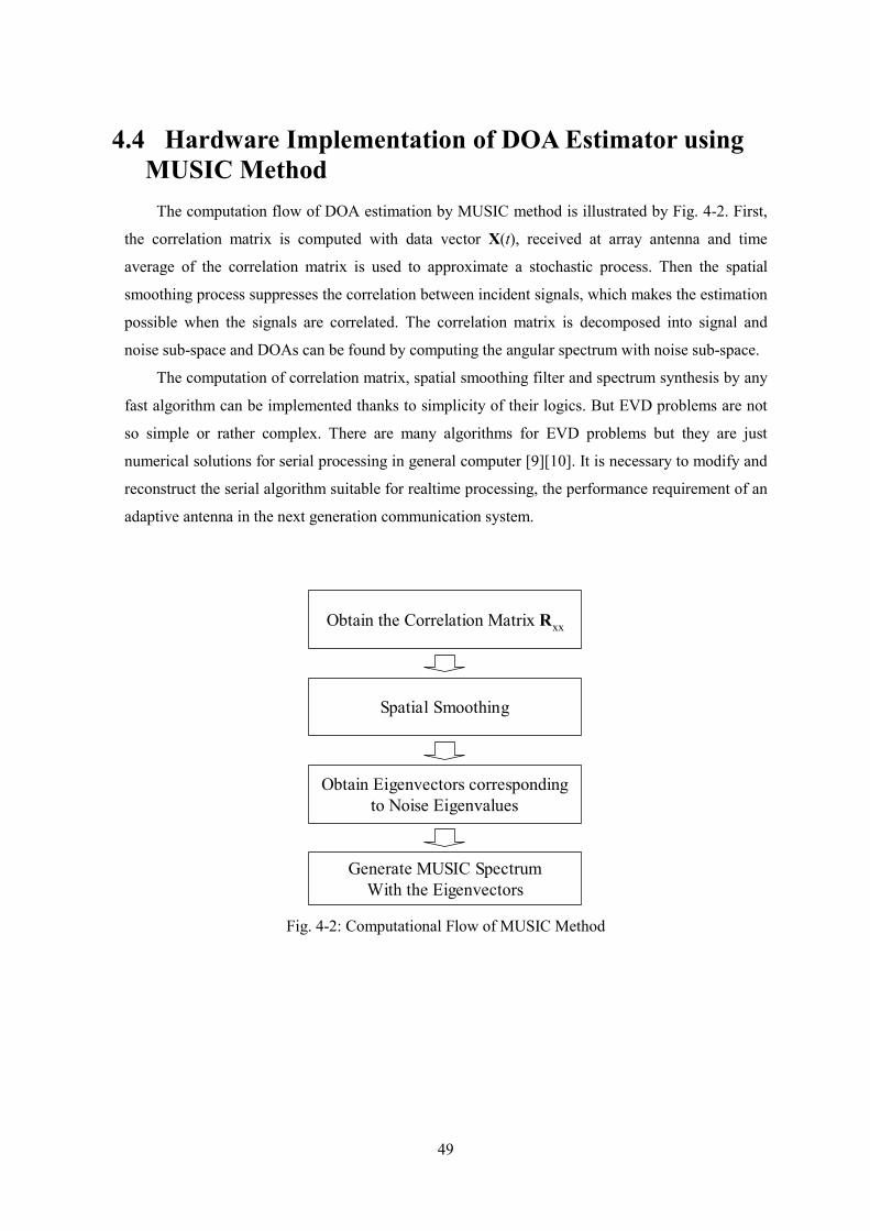
49
4.4 Hardware Implementation of DOA Estimator using MUSIC Method
The computation flow of DOA estimation by MUSIC method is illustrated by Fig. 4-2. First,
the correlation matrix is computed with data vector X(t), received at array antenna and time
average of the correlation matrix is used to approximate a stochastic process. Then the spatial
smoothing process suppresses the correlation between incident signals, which makes the estimation
possible when the signals are correlated. The correlation matrix is decomposed into signal and
noise sub-space and DOAs can be found by computing the angular spectrum with noise sub-space.
The computation of correlation matrix, spatial smoothing filter and spectrum synthesis by any
fast algorithm can be implemented thanks to simplicity of their logics. But EVD problems are not
so simple or rather complex. There are many algorithms for EVD problems but they are just
numerical solutions for serial processing in general computer [9][10]. It is necessary to modify and
reconstruct the serial algorithm suitable for realtime processing, the performance requirement of an
adaptive antenna in the next generation communication system.
Obtain the Correlation Matrix Rxx
Obtain Eigenvectors correspondingto Noise Eigenvalues
Generate MUSIC SpectrumWith the Eigenvectors
Spatial Smoothing
Fig. 4-2: Computational Flow of MUSIC Method

50
4.5 Design of EVD Processor using Jacobi Method Based On CORDIC Algorithm
Computing the Eigen Value Decomposition (EVD) of a symmetric matrix is a frequently
encountered problem in adaptive array signal processing for super resolution DOA estimation
method such as MUSIC, ESPRIT and etc. They are very difficult to implement due to the
complexity and high performance requirement of EVD process, which needs huge scale of circuit
to compute a number of MAC operations. So it is necessary to make these processes as simple as
possible.
In this section an algorithm and the hardware friendly architecture for computing the EVD of
a symmetric correlation matrix are proposed and the basic idea is also presented. Cyclic Jacobi
method is well known for the simplest algorithm and easy implementation but its convergence time
is slower than other factorization algorithm like QR-method [20]. But if considering the fast
parallel computation of the EVD for hardware architecture with an ASIC or an FPGA, the Jacobi
method is a good choice, since it offers a significantly higher degree of parallelism than
QR-method and easy implementation [24].
In this section the EVD is computed using a Jacobi-type method, where the vector rotations
are performed and the rotation angles are obtained by well-known CORDIC (COordinate Rotation
DIgital Computer) algorithm. The hardware architecture suitable for ASIC or FPGA with
fixed-point operation of only shift and add and the estimate of circuit scale are also introduced.
Finally, the required precision for practical application to MUSIC DOA estimation is examined.
4.5.1 Cyclic Jacobi Method
Cyclic Jacobi method computes the symmetric eigenvalue problem by applying a sequence of
orthonormal rotations to the left and right side of target matrix A as
DVAV =⋅⋅T ,
⋅⋅=
⋅⋅=
−PPPJJJJV
nnk ,11312
321∵ (4.13)
where Ppq is an orthonormal plane rotation over an angle θ in the (p, q) plane and defined by (4.14)
and J is multiple rotation of P in the cyclic-by-row manner and called a sweep of Jacobi rotation.
Transforming matrix A infinitely, it is certain that V is the matrix whose column vectors are
composed of eigenvectors and D is eigenvalue matrix whose diagonal elements are eigenvalues.
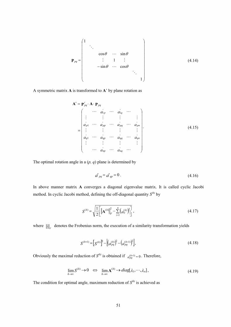
51
−=
1
cossin1
sincos
1
θθ
θθP pq (4.14)
A symmetric matrix A is transformed to A’ by plane rotation as
=
⋅⋅=′
aa
aaaa
aaaa
aa
nqnp
qnqqqpq
pnpqppp
qp
pqpqT
''
''''1
''''1
'1
'1
PAPA
. (4.15)
The optimal rotation angle in a (p, q) plane is determined by
0== ′′ aa qppq . (4.16)
In above manner matrix A converges a diagonal eigenvalue matrix. It is called cyclic Jacobi
method. In cyclic Jacobi method, defining the off-diagonal quantity S(h) by
( )
−= ∑
=
n
i
hii
hF
h aS1
)( 2)( 2)(
21
A , (4.17)
where ⋅F
denotes the Frobenius norm, the execution of a similarity transformation yields
[ ] ( ) ( )[ ]aaSS hpq
hpq
hh )1( 2)( 2)( 2)1( ++ −−= , (4.18)
Obviously the maximal reduction of S(h) is obtained if 0)1( =+a hpq . Therefore,
],,[lim0lim 1)()( λλ n
h
h
h
hdiagS →⇔→
∞→∞→A , (4.19)
The condition for optimal angle, maximum reduction of S(h) is achieved as

52
τθ tan212
tan21 11 −− =
−=
aaa
ppqq
pqopt , (4.20)
where aa
appqq
pq
−=
2τ .
4.5.2 CORDIC (COordinate Rotation DIgital Computer) Algorithm for Computing Vector Rotation
CORDIC (COordinate Rotation DIgital Computer) algorithm was published by Jack E. Volder
in 1959 for the calculation of trigonometric functions, multiplication, division and conversion like
rotation between binary radix number system [21]. The CORDIC algorithm provides an iterative
method of performing vector rotations by arbitrary angles using only shifts and adds. CORDIC
rotation can be explained from the basic vector rotation as
⋅+⋅⋅−⋅
=
⋅
−=
′′
=′
φφφφ
φφφφ
cossinsincos
cossinsincos
yxyx
yx
yx
V. (4.21)
Fig. 4-3 illustrates the rotation of a vector V = [x y]T by the angle φ.
φ
[ ]yx ′′=′V
[ ]yx=V
Fig. 4-3: Vector Rotation by the angle φ
(4.21) is rewritten as
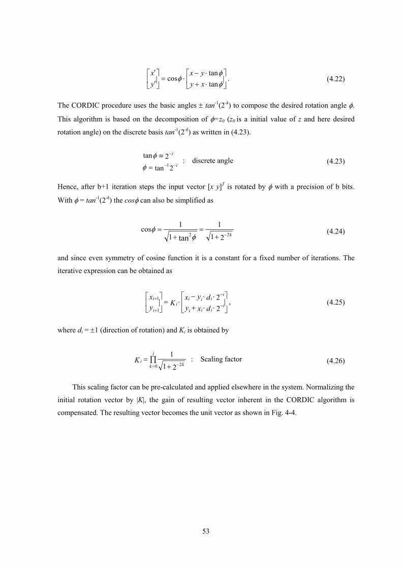
53
⋅+⋅−
⋅=
′′
φφ
φtantan
cosxyyx
yx
. (4.22)
The CORDIC procedure uses the basic angles ± tan-1(2-k) to compose the desired rotation angle φ.
This algorithm is based on the decomposition of φ=z0 (z0 is a initial value of z and here desired
rotation angle) on the discrete basis tan-1(2-k) as written in (4.23).
2tan2tan1 i
i
−−
−
=
≡
φφ
: discrete angle (4.23)
Hence, after b+1 iteration steps the input vector [x y]T is rotated by φ with a precision of b bits.
With φ = tan-1(2-k) the cosφ can also be simplified as
211
1
1cos22tan k−+
=+
=φ
φ (4.24)
and since even symmetry of cosine function it is a constant for a fixed number of iterations. The
iterative expression can be obtained as
⋅⋅+⋅⋅−
⋅=
−
−
+
+
22
1
1i
iii
iiii
ii
i
dxydyx
Kyx
, (4.25)
where di = ±1 (direction of rotation) and Ki is obtained by
∏= −+
=i
k kiK
0 2211 : Scaling factor (4.26)
This scaling factor can be pre-calculated and applied elsewhere in the system. Normalizing the
initial rotation vector by |K|, the gain of resulting vector inherent in the CORDIC algorithm is
compensated. The resulting vector becomes the unit vector as shown in Fig. 4-4.

54
V0
V1
V2
V′
Fig. 4-4: Iterative Vector Rotation
The direction of each rotation is defined by di. It yields the third difference equation that
determines the rotation direction and accumulates rotation angles as (4.27). Those angular values
are supplied from a lookup table (LUT).
)2(tan 11
iiii dzz −−
+ ⋅−= (4.27)
The CORDIC rotation is operated in one of two modes. The first mode, called rotation mode
by Volder [21], rotates the input vector by a specified angle. The second mode, called vectoring
mode, rotates the input vector to the x-axis while recording the angle required for that rotation. In
rotation mode, the angle accumulator is initialized with the desired rotation angle. The rotation
decision at each iteration step is made to decrease the magnitude of the residual angle in the angle
accumulator and is therefore based on the sign of the residual angle after each step. For rotation
mode, the CORDIC equations are
otherwise 1 ,0z if1
)2(tan22
i
11
1
1
+<−=
⋅−=⋅⋅+=⋅⋅−=
−−+
−+
−+
d
dzzdxyydyxx
i
iiii
iiiii
iiiii
. (4.28)
which provides the following result.
[ ][ ]
∏ −+=
=
+=
−=
n
in
n
nn
nn
A
zzxzyAyzyzxAx
21
0sincossincos
2
0000
0000
(4.29)

55
In the vectoring mode, the CORDIC rotation rotates the input vector through whatever angle
is necessary to align the result vector with the x-axis. The result of vectoring operation is a rotation
angle and the scaled magnitude of the original vector in x component. The vectoring function
works by seeking to minimize the y component of the residual vector at each rotation. For
vectoring mode CORDIC equations are
otherwise 1- ,0y if1
)2(tan22
i
11
1
1
<+=
⋅−=⋅⋅+=⋅⋅−=
−−+
−+
−+
d
dzzdxyydyxx
i
iiii
iiiii
iiiii
. (4.30)
which provides the following result.
∏ −
−
+=
+=
=
+=
n
in
n
n
nn
A
xyzz
yAx yx
21
)/(tan
0
2
001
0
20
20
(4.31)
The rotation and vectoring mode of CORDIC algorithm are limited to rotation angles between
–π/2 and π/2 due to the use of 20 for the tangent in the first iteration [22]-[23].
4.5.2.1 Arctangent
The arctangent is directly computed using the vectoring mode CORDIC algorithm if the angle
accumulator is initialized with zero (z0=0). The argument must be provided as a ratio expressed as a
vector [x y]T. The result is taken from the angle accumulator as
)/(tan 001
0 xyzzn−+= . (4.32)
4.5.2.2 Circuit Architecture
The CORDIC algorithm only performs shift and add operations and is therefore easy to
implement and suitable for circuitry. There can be various architectures according to balancing
circuit complexity with respect to performance. The most obvious methods of implementing a
CORDIC algorithm are bit-serial, bit-parallel, unrolled, iterative, and etc. This paper uses the
bit-parallel unrolled CORDIC architecture for high performance. It is a cascade structure of the
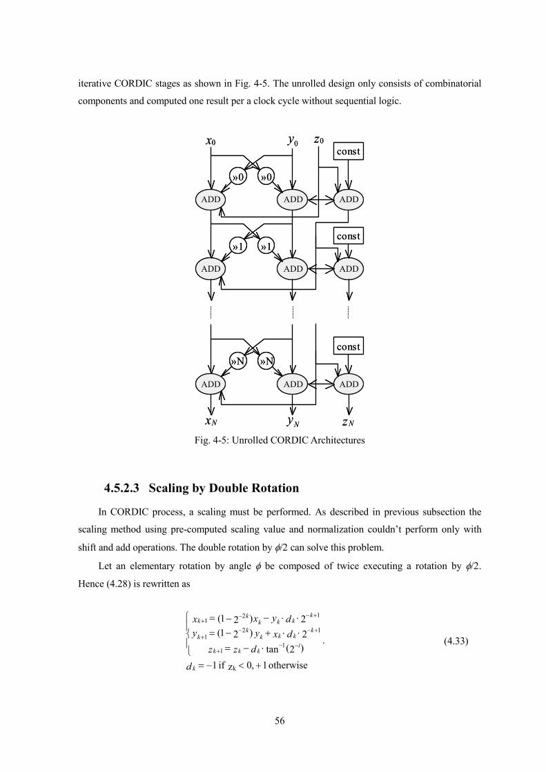
56
iterative CORDIC stages as shown in Fig. 4-5. The unrolled design only consists of combinatorial
components and computed one result per a clock cycle without sequential logic.
»0 »0
ADD ADD
x0 y0
ADD
»1 »1
ADD ADD ADD
»N »N
ADD ADD ADD
xN yN zN
constz0
const
const
»0 »0
ADD ADD
x0 y0
ADD
»1 »1
ADD ADD ADD
»N »N
ADD ADD ADD
xN yN zN
constz0
const
const
Fig. 4-5: Unrolled CORDIC Architectures
4.5.2.3 Scaling by Double Rotation
In CORDIC process, a scaling must be performed. As described in previous subsection the
scaling method using pre-computed scaling value and normalization couldn’t perform only with
shift and add operations. The double rotation by φ/2 can solve this problem.
Let an elementary rotation by angle φ be composed of twice executing a rotation by φ/2.
Hence (4.28) is rewritten as
otherwise 1 ,0z if1
)2(tan2)21(2)21(
k
11
121
121
+<−=
⋅−=⋅⋅+−=⋅⋅−−=
−−+
+−−+
+−−+
d
dzzdxyydyxx
k
ikkk
kkkk
kk
kkk
kkk
. (4.33)
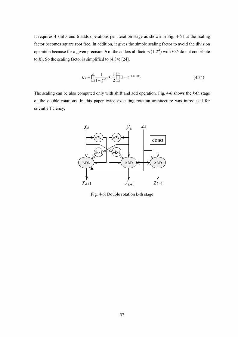
57
It requires 4 shifts and 6 adds operations per iteration stage as shown in Fig. 4-6 but the scaling
factor becomes square root free. In addition, it gives the simple scaling factor to avoid the division
operation because for a given precision b of the adders all factors (1-2-k) with k>b do not contribute
to Kk. So the scaling factor is simplified to (4.34) [24].
)21(21
211 4/
1
)24(
02 ∏∏
=
−−
=−
−≈+
=k
i
ik
iikK (4.34)
The scaling can be also computed only with shift and add operation. Fig. 4-6 shows the k-th stage
of the double rotations. In this paper twice executing rotation architecture was introduced for
circuit efficiency.
»k-1 »k-1
ADD ADD ADD
xk 1+ yk 1+ zk 1+
xk yk
»2k »2k const
zk
Fig. 4-6: Double rotation k-th stage

58
4.5.3 Examination of CORDIC-Jacobi EVD Processor with Fixed Point Operation
This subsection describes the practical implementation of Jacobi EVD processor based on
CORDIC with a fixed-point operation including required number of Jacobi sweeps, precision for
desired accuracy and application to MUSIC DOA estimator.
The precision of fixed-point operation is the first thing to determine. Fig. 4-7 illustrates the
reduction of off-diagonal norm as iteration number of Jacobi sweeps with random real symmetric
matrix of 12-bit precision as an input. Generally in Jacobi method 6~10 sweeps are sufficient to
achieve convergence with floating-point operation [20]. But Fig. 4-7 confirms that the 32-bit
floating-point operation converges to the machine zero within a given precision by 4~5 Jacobi
sweeps, but fixed-point operations not converge but only keep on vibrating after 4~5 Jacobi sweeps
regardless of the precision from 12 to 36 bits. This is caused by the limit-precision of the
fixed-point operation It is the trade-off between implementation simplicity, circuit scale,
performance and accuracy. Without using additional decision circuit, determining the number of
sweeps to be 4~5 fixed is a proper choice and more computations are needless for an efficiency in
hardware architecture.
0 5 10 15 20 25 30 35 40 4510
-6
10-5
10-4
10-3
10-2
10-1
100
101
102
103
104
Number of Sweeps
Off
-di
agonal
Norm 12 Bits Fixed
16 Bits Fixed
20 Bits Fixed24 Bits Fixed
28 Bits Fixed
32 Bits Floating32 Bits Fixed36 Bits Fixed
0 5 10 15 20 25 30 35 40 4510
-6
10-5
10-4
10-3
10-2
10-1
100
101
102
103
104
Number of Sweeps
Off
-di
agonal
Norm 12 Bits Fixed
16 Bits Fixed
20 Bits Fixed24 Bits Fixed
28 Bits Fixed
32 Bits Floating32 Bits Fixed36 Bits Fixed
Fig. 4-7: Reduction of Off-diagonal Norm

59
The next thing to examine is the precision of fixed-point operation. To validate fixed-point
operation, the accuracy within allowable error range must be guaranteed. (4.35) yields the error
ratio where v’s are the vectors whose elements consist of eigenvalues computed in respective
subscript ways and ⋅ denotes vector norm. Physically the error between vectors is defined as Fig.
4-8.
(%)100-
Errorfloat
fixedfloat ×=v
vv (4.35)
Fig. 4-9 shows the error ratio of fixed-point operations on the architecture mentioned in previous
subsections to the 32-bit floating-point operation. Fig. 4-9 used a random real symmetric matrix of
12-bit precision as an input.
vfloat
vfixed
vfloat
vfixed
Fig. 4-8: Errors between Vectors
15 20 25 30 3510
10
10
10
10
10
10
10
10
Err
or
(%)
-7
-6
-5
-4
-3
-2
-1
0
1
Number of Bits12 15 20 25 30 3510
10
10
10
10
10
10
10
10
Err
or
(%)
-7
-6
-5
-4
-3
-2
-1
0
1
Number of Bits12
Fig. 4-9: Error Ratio of fixed-point operations to 32 bits floating point operation
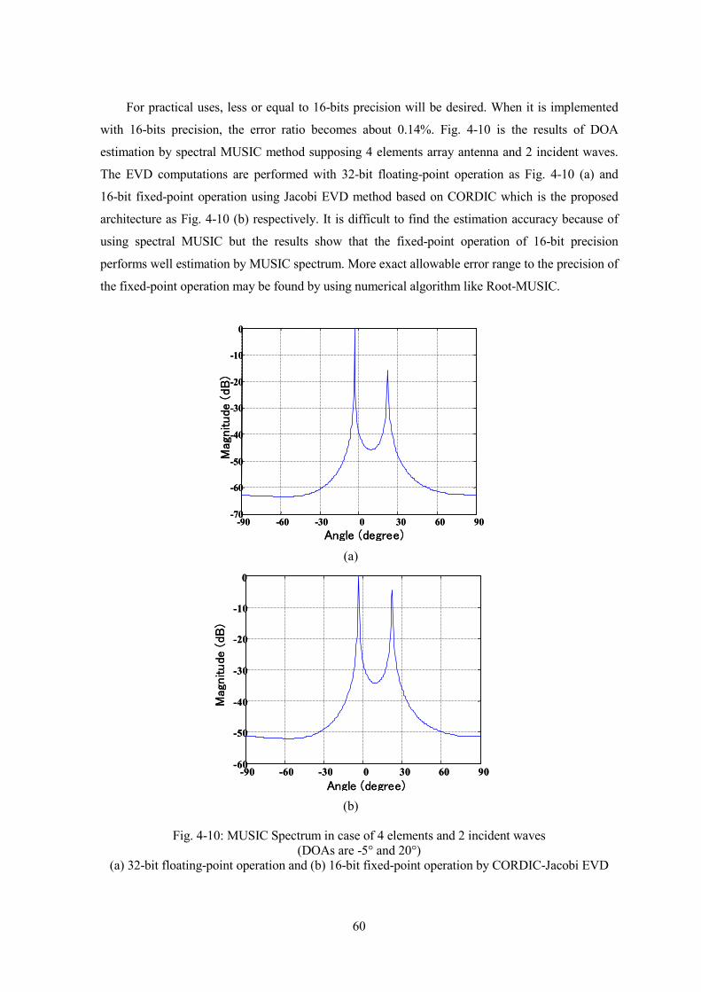
60
For practical uses, less or equal to 16-bits precision will be desired. When it is implemented
with 16-bits precision, the error ratio becomes about 0.14%. Fig. 4-10 is the results of DOA
estimation by spectral MUSIC method supposing 4 elements array antenna and 2 incident waves.
The EVD computations are performed with 32-bit floating-point operation as Fig. 4-10 (a) and
16-bit fixed-point operation using Jacobi EVD method based on CORDIC which is the proposed
architecture as Fig. 4-10 (b) respectively. It is difficult to find the estimation accuracy because of
using spectral MUSIC but the results show that the fixed-point operation of 16-bit precision
performs well estimation by MUSIC spectrum. More exact allowable error range to the precision of
the fixed-point operation may be found by using numerical algorithm like Root-MUSIC.
-90 -60 -30 0 30 60 90-70
-60
-50
-40
-30
-20
-10
0
Angle (degree)
Mag
nitude
(dB
)
-90 -60 -30 0 30 60 90-70
-60
-50
-40
-30
-20
-10
0
Angle (degree)
Mag
nitude
(dB
)
(a)
-90 -60 -30 0 30 60 90-60
-50
-40
-30
-20
-10
0
Angle (degree)
Mag
nitude
(dB
)
-90 -60 -30 0 30 60 90-60
-50
-40
-30
-20
-10
0
Angle (degree)
Mag
nitude
(dB
)
(b)
Fig. 4-10: MUSIC Spectrum in case of 4 elements and 2 incident waves (DOAs are -5° and 20°)
(a) 32-bit floating-point operation and (b) 16-bit fixed-point operation by CORDIC-Jacobi EVD

61
4.5.4 Hardware Design of EVD Processor
In previous subsections it was mentioned that 4~5 Jacobi sweeps are sufficient for
convergence and the fixed-point operation of 16-bit precision gives a good enough spectral
estimation result. Based on these facts, this subsection proposes hardware circuit architecture of the
EVD processor and the design considering the implementation on FPGAs. Fig. 4-11 show the
computational flow of this method. As described before, Jacobi type EVD process is very simple
and just a sequence of vector rotations. From (4.20) the optimal rotation angles are determined and
then the processor performs the similarly conversion of correlation matrix R and unitary matrix E
of eigenvectors. After 4~5 sweeps, the computation is complete. The resulting matrix R converges
the diagonal matrix of eigenvalues and E becomes the unitary matrix of eigenvectors.
ObtainOptimal Rotation Angle
RotateSome Vectors of R, E
Off Diagonal Norm ≈ 0
Sweeps
YES
NO
ObtainOptimal Rotation Angle
RotateSome Vectors of R, E
Off Diagonal Norm ≈ 0
Sweeps
YES
NO
Fig. 4-11: Computation Flow
The EVD processor consists of CORDIC matrix rotators and CORDIC arctangent. With the
optimum angles obtained by (4.20), the rotation Ppq is determined as (4.14). The transform Ppq in
(4.15) changes only p, q rows and columns of the matrix A. Therefore the transform can be
simplified as
⋅
−=
⋅=
′′
aaaaaaaa
qNqqqpq
pNpqppp
q
ppq
q
p T
1
1
cossinsincos
θθθθ
aa
paa
, (4.36)

62
where ak is the k-th row vector of the matrix A and ppq is the vector rotation, a submatrix of Ppq in
(4.14). Thanks to the symmetry of the matrix A, the right side transform yields the same result so it
is not necessary any more except the second rotation of (app, aqq) of A. The diagram of EVD
processor is illustrated in Fig. 4-12, where the ESB (Embedded System Block) is a memory block
of an FPGA and stores the correlation matrix and eigenvector matrix. In the CORDIC matrix
rotator, N CORDIC vector rotators are arranged in parallel. It takes N(N-1)/2 matrix rotations per
one sweep to computing R and E respectively. Fig. 4-13 illustrates the architecture of the EVD
processor core.
CORDIC ATAN(1)
CORDIC ROT.(N)
E(Eigen)
R(Correlation)
N(N-1)
θ opt
ESB
Fig. 4-12: Block Diagram of EVD Processor
CORDIC ATANCORDIC ROT.
E(Eigen)
R(Correlation)
θ opt
RR ppqq −
R pq),( kp ),( kq ),( kp
),( kq
),( kp
),( kq ),( kq
),( kp
CORDIC ATANCORDIC ROT.
E(Eigen)
R(Correlation)
θ opt
RR ppqq −
R pq),( kp ),( kq ),( kp
),( kq
),( kp
),( kq ),( kq
),( kp
ESB
Fig. 4-13: Architecture of EVD Processor Core

63
4.5.5 Circuit Scale / Expected Performance
Basic operation of the proposed EVD processor consists of only shifts and adds. The
computational load required for a CORDIC stage with the double rotation is 4B + 1/4B (needed for
scaling operation) shift and 6B + 1/4B (needed for scaling operation) add where B is bit length. The
number of vector rotations required computing both eigenvalues and eigenvectors is
4×N(N-1)(N+2) where 4 Jacobi sweeps and N is the double number of array length. Hence total
computational load is [4×N(N-1)(N+2)+1]* (17/4B Shift + 25/4B Add).
On the other hands, if configuring this computation load with the parallel architecture
proposed in previous subsections, rough estimate of circuit scale is about (N+1)×15K equivalent
gates. For example, if N=8 (4-element array antenna if n×n correlation matrix of complex numbers
is converted into 2n×2n matrix of only real numbers [20]) the total circuit scale is about 75K
equivalent gates.
This system, if arranged parallel structure, requires [4×N(N-1)×2+1]*(B+1) clock cycles to
compute one EVD computation. For example, if N=8, B=16 and operated at the speed of 100 MHz,
this system can compute EVD computations about 13,200 times (75.8 µs / EVD). The EVD is the
most dominant process in the whole processing load from DOA finding to beamforming. This fast
computation processor must provide efficient use.
4.5.6 Discussion
In this section the circuit design of EVD computation processor for MUSIC DOA estimator
was proposed. It uses CORDIC based Jacobi method and is suitable for hardware implementation
for realtime processing. Adopting fixed-point operation causes some error but make the
implementation easy and achieve the high performance. In addition, the accuracy of the 16-bit
fixed-point operation has the error less 0.14% and the functionality for spectral MUSIC method
could be confirmed.

64
4.6 Summary This chapter described the DOA estimation application of an adaptive antenna technology.
The MUSIC method has super resolution of estimating DOAs of incident waves but is based on
complex EVD computation. The principle of MUSIC method was presented and the performance
requirement for multi-path fading solution was discussed. The hardware implementation on an
FPGA of MUSIC DOA estimator consists of lots of processes, the most complex process of which
is the EVD computation and it dominates the whole system throughput. This chapter proposed the
Jacobi-type EVD processor based on CORDIC algorithm. It is suitable for hardware architecture of
parallel processing and FPGAs provide the efficient configuration.
65
Chapter 5
Summary And Conclusion
This chapter summarizes and concludes the paper.
This paper introduced the digital prototype system for the evaluation of an adaptive antenna
based on FPGAs considering the reconfigurablity of software defined radio (SDR) and the
performance of realtime processing required to an adaptive antenna system.
As an application, the implementation of 2-element MRC (Maximal Ratio Combining)
beamforming receiver similar to a phased array antenna in analog sense using of digital
beamforming network was examined. The circuit in FPGAs was implemented in parallel structure
and the performance is expected to meet the requirement of realtime processing in practical
wireless communications. By some experiment in a radio anechoic chamber, the functions of such
as beamforming and DOA tracking are validated. In addition, two digital calibration techniques
were proposed. The adjustment method by NCO control, which is performed at IF stage and the
other method using the MRC optimum weight which is performed at baseband were discussed.
They are easy to implement on FPGAs and can be processed in realtime.
As the other application, this paper described the DOA estimation technique. The MUSIC
method has super resolution estimating DOAs of incident waves but is based on complex EVD
computation, which dominates the whole system load. The Jacobi-type EVD processor based on
CORDIC algorithm was proposed, which is suitable for hardware architecture like parallel
processing and FPGAs provide the efficient configuration. It is expected to meet the performance
requirement for the next generation wireless communication.
The cost of hardware will become reasonable and the performance will be also improved as a
progress of device technologies. The digital technology is replacing an old fashion of analog
technology step by step. An adaptive antenna which combines antenna technology and digital
signal processing technology will be quite promising in the next generation communication system.

66
Acknowledgments
I thank many people who supported me in their helpful comments and enlightening
suggestions. First of all, my supervisor, associate professor Dr. Hiroyuki Arai always gave me the
courage to perform my research abroad, in Japan as well as the technical supports. Dr. Masahiro
Fukuta of Brains Corp. gave me the opportunity to participate in this research. He also helped me
the hardware support (manufacturing prototype system) and guided the hardware implementation.
And I also appreciate Dr. Koichi Ichige for a plenty of advices and criticism about my research. I
would like to extend my gratitude to everybody in prof. Arai and prof. Ichige laboratory.
Finally, especially I thank to my parents and my family in Korea.

67
Bibliography
[1] R. Miura, T. Tanaka, A. Horie and Y. Karasawa, “A DBF Self-Beam Steering Array Antenna
for Mobile Satellite Applications Using Beam-Space Maximal-Ratio Combination,” IEEE trans
on vehicular technology, Vol. 48, No 3, May 1999
[2] Per H. Lehne and Magne Pettersen, “An Overview of Smart Antenna Technology for Mobile
Communications Systems,” IEEE Communications Surveys, Fourth Quarter 1999, Vol. 2, No.
4, http://www.comsoc.org/pubs/surveys
[3] Y. Karasawa, “The Software Antenna: A New Concept of Kaleidoscopic Antenna in
Multimedia Radio and Mobile Computing Era,” IEICE Trans., Comm., Vol. E80-B, No. 8,
pp.1214-1217, Aug. 1997
[4] H. Steyskal, “Digital Beamforming Antennas, An Introduction,” Microwave Journal, Vol. 30,
No. 1, pp. 107-124, Jan. 1987
[5] J. Mitola III, “Software Radios Survey, Critical Evaluation and Future Directions,” IEEE
National Telesystems Conference, pp. 13-15~13-23, 1992
[6] G. Prescott and S. Gurrapu “Design And Implementation of a DSP Digital Beam Forming
Receiver,” Information and Tele-communication Technology Center, University of Kansas,
1997 ICSPAT Proceeding
[7] N. Kikuma, Adaptive Signal Processing with Array Antenna, Science and Technology
Publishing Company, Inc., 1999, in Japanese
[8] Jens Baltersee, “Development and Analysis of Protocols for Directed antennas in the Mobile
Broadband System,”
http://www.comnets.rwth-aachen.de/~ftp-mbs/publications/dir_ant_da/da.html
[9] Simon Haykin, Adaptive filter theory, Third Edition, Prentice Hall, 1996
[10] Gene H. Golub and Charles F. Van Loan, Matrix Computations, The Johns Hopkins
University Press, 1996
[11] B. Fawcett and R. Iwanczuk, “Techniques and Tools for FPGA-based DSP design,” Xilinx
Inc.
[12] Mark Cummings and Shinichiro Haruyama, “FPGA in the Software Radio,” IEEE
Communication Magazine, Vol. 37, No. 2, pp.108-112, Feb. 1999

68
[13] R. Baines, “The DSP Bottleneck,” IEEE Communications Magazine, May 1995, pp. 46~54
[14] John Litva, Titus Kwok-Yeuong Lo, Digital Beamforming in Wireless Communications,”
Artech House Publishers, 1996
[15] M. Kim, H. Arai and M. Fukuta “Development of a Digital Prototype Board for Adaptive
Array Antenna Receiver,” Submitted to 2001 IEICE Society Conference
[16] John G. Proakis, Digital Communications, 4th ed, McGraw-Hill, 2001
[17] Digital IF Subsampling Using the HI5702, HSP45116 and HSP43220, Intersil Application
Note, AN9509.2
[18] Implementing FIR filters in FLEX Devices, ALTERA Applications Note 73, Feb. 1998
[19] Rodney G. Vaughan, Neil L. Scott, D. Rod White, “The theory of bandpass sampling,” IEEE
Trans. on signal processing, Vol. 39, No. 9, pp. 1973~1984, Sep. 1991
[20] William H. Press, Saul A. Teukolsky, William T. Vetterling and Brian P. Flannery, Numerical
Recipes in C, The Art of Scientific Computing, Second Edition, Cambridge University Press,
1992
[21] Volder J. E. “The CORDIC trigonometric computing technique,” IRE Trans. Electronic
Computing, Vol. EC-8, 1959
[22] Muller and Jean Michel, Elementary Functions: Algorithms and Implementation
[23] Andraka R. “A survey of CORDIC algorithms for FPGA based computers,” Proceeding of the
1998 ACM/SIGDA sixth international symposium on Field Programmable Gate Arrays, pp
192-200, Monterey, CA, Feb. 1998
[24] Jurgen Gotze, Steffen Paul and Matthias Sauer, “An Efficient Jacobi-like Algorithm for
Parallel Eigenvalue Computation”, IEEE Trans. On Computer, Vol. 42, No. 9. Sep. 1993

69
Publication List
IEICE Technical Report
“FPGA-Based DSP Implementation of Simple MRC Digital Beamforming Antenna"
Minseok Kim, Koichi ICHIGE, Hiroyuki ARAI,
IEICE Antenna &Propagation Technical Report, AP2001-49,
Kitami Institute of Technology, Hokkaido, JAPAN, Jul. 2001
IEICE General Conference
“Examination of FPGA Implementation on Eigenvalue Decomposition in MUSIC Method”,
Minseok Kim, Koichi ICHIGE, Hiroyuki ARAI,
2001 IEICE General Conference, B-1-45,
Ritsumeikan Univ., Kyoto, JAPAN, Mar. 2001
“Development of a Digital Prototype Board for Adaptive Array Antenna Receiver”
Minseok Kim, Hiroyuki ARAI, Masahiro FUKUTA,
2001 IEICE Communication Society Conference, B-1-151,
The University of Electro-Communications, Chofu, JAPAN, Sep. 2001
“Design of EVD Computation Processor for MUSIC DOA Estimation By using Cyclic Jacobi
Method based on CORDIC”
Minseok Kim, Koichi ICHIGE, Hiroyuki ARAI,
2002 IEICE General Conference, A-4-70 (Accepted)
Waseda University, Tokyo, Japan, Mar. 2002
International Conference
“FPGA-Based DSP Implementation of Simple MRC beamformer”
Minseok Kim, Koichi ICHIGE, Hiroyuki ARAI
APMC 2001 Conference, pp.589-592,
National Taiwan University, Taipei, TAIWAN, Dec. 2001