A Stretchable Electromagnetic Absorber Fabricated Using ...
10
sensors Article A Stretchable Electromagnetic Absorber Fabricated Using Screen Printing Technology Heijun Jeong and Sungjoon Lim * School of Electrical and Electronics Engineering, College of Engineering, Chung-Ang University, 221 Heukseok-dong, Dongjak-gu, Seoul 156-756, Korea; [email protected] * Correspondence: [email protected]; Tel.: +82-2-820-5827 Academic Editor: Vittorio M.N. Passaro Received: 15 March 2017; Accepted: 19 May 2017; Published: 21 May 2017 Abstract: A stretchable electromagnetic absorber fabricated using screen printing technology is proposed in this paper. We used a polydimethylsiloxane (PDMS) substrate to fabricate the stretchable absorber since PDMS exhibits good dielectric properties, flexibility, and restoring capabilities. DuPont PE872 (DuPont, Wilmington, CT, USA), a stretchable silver conductive ink, was used for the screen printing technique. The reflection coefficient of the absorber was measured using a vector network analyzer and a waveguide. The proposed absorber was designed as a rectangular patch unit cell, wherein the top of the unit cell acted as the patch and the bottom formed the ground. The size of the patch was 8 mm × 7 mm. The prototype of the absorber consisted of two unit cells such that it fits into the WR-90 waveguide (dimensions: 22.86 mm × 10.16 mm) for experimental measurement. Before stretching the absorber, the resonant frequency was 11 GHz. When stretched along the x-direction, the resonant frequency shifted by 0.1 GHz, from 11 to 10.9 GHz, demonstrating 99% absorption. Furthermore, when stretched along the y-direction, the resonant frequency shifted by 0.6 GHz, from 11 to 10.4 GHz, demonstrating 99% absorption. Keywords: electromagnetic; absorber; screen printing; stretchable 1. Introduction Metamaterials are artificial structures wherein periodical unit cells are arranged infinitely such that the characteristics of the material can be controlled artificially. Owing to this extraordinary feature, metamaterials are used in cloaking technology [1], super lenses [2], antennas [3], and control components in the THz band [4]. Metamaterial absorber is a technology that uses metamaterials [5,6]. A metamaterial absorber was first introduced by Landy [7]. Owing to the infinitely periodic structure of a metamaterial absorber, the substance can be easily expanded [8]. In addition, since the absorber uses a thinner substrate than conventional absorbers (such as ferrite or wedge-tapered absorbers) [9,10], it can be fabricated in light and compact volumes. Recently, metamaterial absorbers have been studied not only for narrow bandwidths but also for wide bandwidths through multi-layer absorbers [11], lossy patterns [12,13], frequency switching [14–17], etc. Especially, a frequency switchable metamaterial absorber can operate in a diverse spectrum. In addition, it can be used as sensors by detecting frequency changes for different physical or chemical actuation. One of the methods of frequency switching is the use of electrical switching components such as pin diodes, varactor didoes, or microelectromechanical systems [18–20]. The instantaneous frequency of these absorbers is tunable owing to the use of electronic devices. However, these electrical switching components require complex direct current (DC) bias lines and are expensive. Therefore, there is a restriction on the fabrication of the absorber since unnecessary bias lines must be designed. Sensors 2017, 17, 1175; doi:10.3390/s17051175 www.mdpi.com/journal/sensors
Transcript of A Stretchable Electromagnetic Absorber Fabricated Using ...
sensors
Article
A Stretchable Electromagnetic Absorber FabricatedUsing Screen Printing Technology
Heijun Jeong and Sungjoon Lim *
School of Electrical and Electronics Engineering, College of Engineering, Chung-Ang University,221 Heukseok-dong, Dongjak-gu, Seoul 156-756, Korea; [email protected]* Correspondence: [email protected]; Tel.: +82-2-820-5827
Academic Editor: Vittorio M.N. PassaroReceived: 15 March 2017; Accepted: 19 May 2017; Published: 21 May 2017
Abstract: A stretchable electromagnetic absorber fabricated using screen printing technology isproposed in this paper. We used a polydimethylsiloxane (PDMS) substrate to fabricate the stretchableabsorber since PDMS exhibits good dielectric properties, flexibility, and restoring capabilities. DuPontPE872 (DuPont, Wilmington, CT, USA), a stretchable silver conductive ink, was used for the screenprinting technique. The reflection coefficient of the absorber was measured using a vector networkanalyzer and a waveguide. The proposed absorber was designed as a rectangular patch unit cell,wherein the top of the unit cell acted as the patch and the bottom formed the ground. The size ofthe patch was 8 mm × 7 mm. The prototype of the absorber consisted of two unit cells such that itfits into the WR-90 waveguide (dimensions: 22.86 mm × 10.16 mm) for experimental measurement.Before stretching the absorber, the resonant frequency was 11 GHz. When stretched along thex-direction, the resonant frequency shifted by 0.1 GHz, from 11 to 10.9 GHz, demonstrating 99%absorption. Furthermore, when stretched along the y-direction, the resonant frequency shifted by0.6 GHz, from 11 to 10.4 GHz, demonstrating 99% absorption.
Keywords: electromagnetic; absorber; screen printing; stretchable
1. Introduction
Metamaterials are artificial structures wherein periodical unit cells are arranged infinitely suchthat the characteristics of the material can be controlled artificially. Owing to this extraordinary feature,metamaterials are used in cloaking technology [1], super lenses [2], antennas [3], and control componentsin the THz band [4].
Metamaterial absorber is a technology that uses metamaterials [5,6]. A metamaterial absorber wasfirst introduced by Landy [7]. Owing to the infinitely periodic structure of a metamaterial absorber,the substance can be easily expanded [8]. In addition, since the absorber uses a thinner substrate thanconventional absorbers (such as ferrite or wedge-tapered absorbers) [9,10], it can be fabricated in lightand compact volumes.
Recently, metamaterial absorbers have been studied not only for narrow bandwidths but also forwide bandwidths through multi-layer absorbers [11], lossy patterns [12,13], frequency switching [14–17],etc. Especially, a frequency switchable metamaterial absorber can operate in a diverse spectrum.In addition, it can be used as sensors by detecting frequency changes for different physical orchemical actuation.
One of the methods of frequency switching is the use of electrical switching components such aspin diodes, varactor didoes, or microelectromechanical systems [18–20]. The instantaneous frequencyof these absorbers is tunable owing to the use of electronic devices. However, these electrical switchingcomponents require complex direct current (DC) bias lines and are expensive. Therefore, there isa restriction on the fabrication of the absorber since unnecessary bias lines must be designed.
Sensors 2017, 17, 1175; doi:10.3390/s17051175 www.mdpi.com/journal/sensors

Sensors 2017, 17, 1175 2 of 10
Alternative methods include performing frequency switching without using electrical switchingcomponents, e.g., microfluidic absorbers [15,21] or stretchable absorbers [22–24]. Microfluidic absorberssuch as injection liquid metals [21] and crystal into microfluidic channels [15] can have tunablefrequency; however, these absorbers not only are difficult to fabricate but also require complexmicrofluidic channel lines. Hence, we proposed a stretchable electromagnetic absorber for frequencyswitching. The proposed stretchable absorber can vary the resonance frequency by varying theelectrical length of the resonator. Therefore, it is not necessary to design a separate electrical biasline. In addition, the stretchable absorbers can be used as remote strain sensors [25,26]. In this study,we fabricated an absorber using a screen printing technique on a stretchable polydimethylsiloxane(PDMS) material, which is expected to be applicable not only as an absorber but also as a sensor.PDMS substrate has been employed in flexible or stretchable radio frequency (RF) electronics [27,28].Conventional fabrication of PDMS should be processed via spin-coating, via exposure to UV light,via deposition, etc. [29,30]. These are complicated processes and produce additional chemical waste.Moreover, the equipment is very expensive. In this work, we fabricated the frame of PDMS substrateusing a 3D printing process, since such processes facilitate simple fabrication by eliminating the needfor complicated processes. In addition, we used DuPont PE872 silver conductive ink. Since PE872ink has not only conductive but also stretchable characteristics, it is used for the fabrication of thestretchable absorber in this study. The performance of the proposed absorber will be numerically andexperimentally demonstrated. The fabrication process will be explained in the following sections.
2. Absorber Design
The proposed electromagnetic absorber was designed as two rectangular patch unit cells. Figure 1shows the unit cell geometry of the proposed electromagnetic absorber. The unit cell was designedto consist of a PDMS substrate of dimensions 12 mm × 12 mm × 0.5 mm and a patch of dimensions8 mm × 7 mm, as shown in Figure 1a. The bottom of the absorber was designed to have the samewidth and length as the PDMS substrate, as shown in Figure 1b. The resonant frequency (f 0) of theunit cell is given by the following equation [31]:
f0 =c
2√εe f f
Lp + 0.824Hs
[(εe f f +0.3)
(WpHs +0.264
)(εe f f−0.258)
(WpHs +0.8
)] (1)
εe f f =εr + 1
2+
εr − 12
1√1 + 12
(HsWp
) (2)
where f 0 and εeff are the resonant frequency and dielectric constant, respectively.According to Equations (1) and (2), the resonant frequency is determined by the substrate
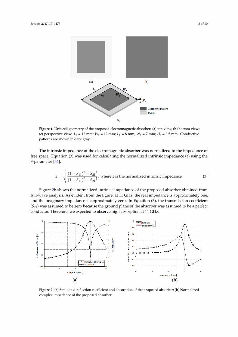
height (Hs), dielectric constant (εe f f ), and the width (Wp) and length (Lp) of the patch. In this study,the dielectric constant and loss tangent of the PDMS substrate were obtained using the T-resonatormethod [32,33], and the values of these parameters were determined to be 2.89 and 0.02, respectively.The resonant frequency obtained using Equations (1) and (2) were 11 GHz. In order to validate thecalculated value, we performed a resonant frequency simulation using the ANSYS high frequencystructure simulator (HFSS). Simulation results confirmed a resonant frequency of 11 GHz witha reflection coefficient of −33 dB and approximately 100% absorption, as shown in Figure 2a.
Sensors 2017, 17, 1175 3 of 10
Sensors 2017, 17, x FOR PEER REVIEW 3 of 10
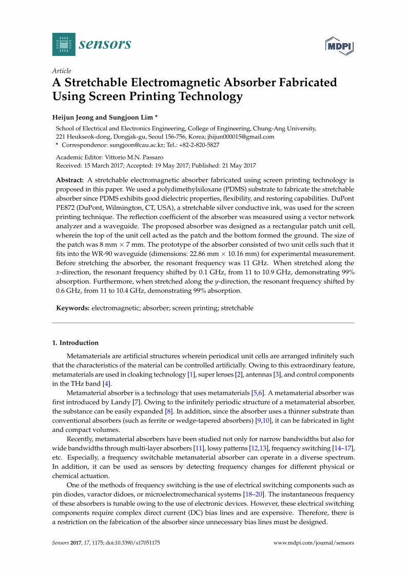
Figure 1. Unit cell geometry of the proposed electromagnetic absorber: (a) top view; (b) bottom view;
(c) perspective view. Ls = 12 mm; Ws = 12 mm; Lp = 8 mm; Wp = 7 mm; Hs = 0.5 mm. Conductive
patterns are shown in dark gray.
The intrinsic impedance of the electromagnetic absorber was normalized to the impedance of
free space. Equation (3) was used for calculating the normalized intrinsic impedance (z) using the
S-parameter [34].
2 2
11 21
2 2
11 21
(1 ), where is the normalized intrinsic impedance
(1 )
S Sz z
S S
.
(3)
Figure 2b shows the normalized intrinsic impedance of the proposed absorber obtained from
full-wave analysis. As evident from the figure, at 11 GHz, the real impedance is approximately one,
and the imaginary impedance is approximately zero. In Equation (3), the transmission coefficient
(S21) was assumed to be zero because the ground plane of the absorber was assumed to be a perfect
conductor. Therefore, we expected to observe high absorption at 11 GHz.
(a) (b)
Figure 2. (a) Simulated reflection coefficient and absorption of the proposed absorber; (b)
Normalized complex impedance of the proposed absorber.
Figure 1. Unit cell geometry of the proposed electromagnetic absorber: (a) top view; (b) bottom view;(c) perspective view. Ls = 12 mm; Ws = 12 mm; Lp = 8 mm; Wp = 7 mm; Hs = 0.5 mm. Conductivepatterns are shown in dark gray.
The intrinsic impedance of the electromagnetic absorber was normalized to the impedance offree space. Equation (3) was used for calculating the normalized intrinsic impedance (z) using theS-parameter [34].
z =
√√√√ (1 + S11)2 − S21
2
(1− S11)2 − S21
2, where z is the normalized intrinsic impedance. (3)
Figure 2b shows the normalized intrinsic impedance of the proposed absorber obtained fromfull-wave analysis. As evident from the figure, at 11 GHz, the real impedance is approximately one,and the imaginary impedance is approximately zero. In Equation (3), the transmission coefficient(S21) was assumed to be zero because the ground plane of the absorber was assumed to be a perfectconductor. Therefore, we expected to observe high absorption at 11 GHz.
Sensors 2017, 17, x FOR PEER REVIEW 3 of 10
Figure 1. Unit cell geometry of the proposed electromagnetic absorber: (a) top view; (b) bottom view;
(c) perspective view. Ls = 12 mm; Ws = 12 mm; Lp = 8 mm; Wp = 7 mm; Hs = 0.5 mm. Conductive
patterns are shown in dark gray.
The intrinsic impedance of the electromagnetic absorber was normalized to the impedance of
free space. Equation (3) was used for calculating the normalized intrinsic impedance (z) using the
S-parameter [34].
2 2
11 21
2 2
11 21
(1 ), where is the normalized intrinsic impedance
(1 )
S Sz z
S S
.
(3)
Figure 2b shows the normalized intrinsic impedance of the proposed absorber obtained from
full-wave analysis. As evident from the figure, at 11 GHz, the real impedance is approximately one,
and the imaginary impedance is approximately zero. In Equation (3), the transmission coefficient
(S21) was assumed to be zero because the ground plane of the absorber was assumed to be a perfect
conductor. Therefore, we expected to observe high absorption at 11 GHz.
(a) (b)
Figure 2. (a) Simulated reflection coefficient and absorption of the proposed absorber; (b)
Normalized complex impedance of the proposed absorber. Figure 2. (a) Simulated reflection coefficient and absorption of the proposed absorber; (b) Normalizedcomplex impedance of the proposed absorber.

Sensors 2017, 17, 1175 4 of 10
The absorption of the electromagnetic absorber can be understood from its electrical fielddistribution and current density [35,36]. Figure 3a shows the magnitude of the electric field distributionof the proposed absorber at 11 GHz. It is observed from Figure 3a that the electric field is distributed atthe edge of the patch which generates electric resonance. Figure 3b shows the vector current density at11 GHz. As evident from Figure 3b, the vector current density is in the H(y)-direction in the top planeand in the –H(y)-direction in the bottom plane. In addition, the vector current densities in the top andbottom planes are anti-parallel, which generates magnetic resonance. Figure 4 shows the simulatedS-parameter of the absorber stretched in different directions. When the absorber was stretched in thedirection of the x-axis, as shown in Figure 4a, the resonance frequency shifted by 0.3 GHz, from 11 to10.7 GHz. Furthermore, when the absorber was stretched by the same length in the direction of they-axis, as shown in Figure 4b, the resonant frequency shifted by 0.75 GHz, from 11 to 10.25 GHz. Thus,we observed a wider change in frequency when we stretched the absorber in the direction of the y-axis.
Sensors 2017, 17, x FOR PEER REVIEW 4 of 10
The absorption of the electromagnetic absorber can be understood from its electrical field
distribution and current density [35,36]. Figure 3a shows the magnitude of the electric field
distribution of the proposed absorber at 11 GHz. It is observed from Figure 3a that the electric field
is distributed at the edge of the patch which generates electric resonance. Figure 3b shows the
vector current density at 11 GHz. As evident from Figure 3b, the vector current density is in the
H(y)-direction in the top plane and in the –H(y)-direction in the bottom plane. In addition, the
vector current densities in the top and bottom planes are anti-parallel, which generates magnetic
resonance. Figure 4 shows the simulated S-parameter of the absorber stretched in different
directions. When the absorber was stretched in the direction of the x-axis, as shown in Figure 4a, the
resonance frequency shifted by 0.3 GHz, from 11 to 10.7 GHz. Furthermore, when the absorber was
stretched by the same length in the direction of the y-axis, as shown in Figure 4b, the resonant
frequency shifted by 0.75 GHz, from 11 to 10.25 GHz. Thus, we observed a wider change in
frequency when we stretched the absorber in the direction of the y-axis.
(a) (b)
Figure 3. (a) Simulation of unit cell electric field distribution; (b) Vector current density.
(a) (b)
Figure 4. Simulated S-parameter of the absorber stretched along (a) the x-axis and (b) the y-axis.
Figure 3. (a) Simulation of unit cell electric field distribution; (b) Vector current density.
Sensors 2017, 17, x FOR PEER REVIEW 4 of 10
The absorption of the electromagnetic absorber can be understood from its electrical field distribution and current density [35,36]. Figure 3a shows the magnitude of the electric field distribution of the proposed absorber at 11 GHz. It is observed from Figure 3a that the electric field is distributed at the edge of the patch which generates electric resonance. Figure 3b shows the vector current density at 11 GHz. As evident from Figure 3b, the vector current density is in the H(y)-direction in the top plane and in the –H(y)-direction in the bottom plane. In addition, the vector current densities in the top and bottom planes are anti-parallel, which generates magnetic resonance. Figure 4 shows the simulated S-parameter of the absorber stretched in different directions. When the absorber was stretched in the direction of the x-axis, as shown in Figure 4a, the resonance frequency shifted by 0.3 GHz, from 11 to 10.7 GHz. Furthermore, when the absorber was stretched by the same length in the direction of the y-axis, as shown in Figure 4b, the resonant frequency shifted by 0.75 GHz, from 11 to 10.25 GHz. Thus, we observed a wider change in frequency when we stretched the absorber in the direction of the y-axis.
(a) (b)
Figure 3. (a) Simulation of unit cell electric field distribution; (b) Vector current density.
(a) (b)
Figure 4. Simulated S-parameter of the absorber stretched along (a) the x-axis and (b) the y-axis.
Figure 4. Simulated S-parameter of the absorber stretched along (a) the x-axis and (b) the y-axis.

Sensors 2017, 17, 1175 5 of 10
3. Fabrication Processes
3.1. PDMS Fabrication
Figure 5 shows the fabrication process of the PDMS substrate. The outline (to solidify the liquidPDMS) was manufactured on a glass substrate via a 3D printing process [37,38], as shown in Figure 5a.We used the Ultimaker2+ 3D printer (Ultimaker B.V., Geldermalsen, The Netherlands) for the outlinefabrication. Subsequently, the PDMS base in liquid state and the curing agent were mixed in a beakerin a ratio of 10:1. The mixed solution was poured into the outline, as shown in Figure 5b, and curedat 100 C for 25 min using a hot plate, as shown in Figure 5c. Subsequently, plasma treatment wasperformed to enhance the adhesion of the PDMS surface, as shown in Figure 5d. We used the PDC-32Gplasma (Harrick Plasma, New York, NY, USA), treated at 18 W for 20 s.
Sensors 2017, 17, x FOR PEER REVIEW 5 of 10
3. Fabrication Processes
3.1. PDMS Fabrication
Figure 5 shows the fabrication process of the PDMS substrate. The outline (to solidify the
liquid PDMS) was manufactured on a glass substrate via a 3D printing process [37,38], as shown in
Figure 5a. We used the Ultimaker2+ 3D printer (Ultimaker B.V., Geldermalsen, The Netherlands)
for the outline fabrication. Subsequently, the PDMS base in liquid state and the curing agent were
mixed in a beaker in a ratio of 10:1. The mixed solution was poured into the outline, as shown in
Figure 5b, and cured at 100 °C for 25 min using a hot plate, as shown in Figure 5c. Subsequently,
plasma treatment was performed to enhance the adhesion of the PDMS surface, as shown in Figure
5d. We used the PDC-32G plasma (Harrick Plasma, New York, NY, USA), treated at 18 W for 20 s.
Figure 5. Fabrication process of the PDMS substrate; (a) Step 1: PDMS substrate outline, fabricated
using a 3D printer; (b) Step 2: mixing the Sylgard184 A type and the Sylgard184 B type silicone
elastomers; (c) Step 3: pouring PDMS into the outline and curing processing using hot plate; (d) Step
4: plasma treatment process.
3.2. Screen Printing Process
In this study, we proposed the use of screen printing technology for fabricating the top patch
and bottom ground of the unit cell. The screen printing process is simple and easy, thereby
allowing the fabrication of large quantities with a high number of patches and ground fabricated
simultaneously. We used PE872 stretchable conductive silver ink for screen printing. Prior to screen
printing, we performed plasma treatment to prevent the absorber from detaching when stretched
[39]. After plasma treatment, we printed the absorber using (Daeyoung-Tech Co., Gyeonggi-do,
Korea). The device provided squeegee speeds of 45–595 mm/s, and squeegee angles of 60–90°, as
shown in Figure 6a,b. A stainless wire mesh with a mesh tension of 150 N and a wire count of 400
was also used in the screen printing process. We printed two unit cells on the top side of the PDMS.
The gap at the top of the unit cell was 2 mm, and the size of each unit cell was 8 mm × 7 mm. The
bottom ground of the cell was similarly printed. Further, a curing process was performed to
improve the conductivity of the screen-printed surface. The curing process for screen printing
technology can be performed via various methods such as the use of a well-ventilated oven, dryer
curing, and thermal sintering [40]. In this study, we used the ON-22GW well-ventilated oven
(Dongsung Science Co., Busan, Korea). The curing was performed in an oven at 100 °C for 30 min.
We used DuPont PE872 (DuPont, USA) silver conductive ink for screen printing. When the
printed thickness is 14 μm, the sheet resistivity is 0.4 Ω. Figure 7a shows the screen-printed Ag
patterns, and Figure 7b shows the morphological characterization using a field emission scanning
electron microscope (FE-SEM).
Figure 5. Fabrication process of the PDMS substrate; (a) Step 1: PDMS substrate outline, fabricatedusing a 3D printer; (b) Step 2: mixing the Sylgard184 A type and the Sylgard184 B type siliconeelastomers; (c) Step 3: pouring PDMS into the outline and curing processing using hot plate; (d) Step 4:plasma treatment process.
3.2. Screen Printing Process
In this study, we proposed the use of screen printing technology for fabricating the top patch andbottom ground of the unit cell. The screen printing process is simple and easy, thereby allowing thefabrication of large quantities with a high number of patches and ground fabricated simultaneously.We used PE872 stretchable conductive silver ink for screen printing. Prior to screen printing, we performedplasma treatment to prevent the absorber from detaching when stretched [39]. After plasma treatment,we printed the absorber using (Daeyoung-Tech Co., Gyeonggi-do, Korea). The device provided squeegeespeeds of 45–595 mm/s, and squeegee angles of 60–90, as shown in Figure 6a,b. A stainless wire meshwith a mesh tension of 150 N and a wire count of 400 was also used in the screen printing process.We printed two unit cells on the top side of the PDMS. The gap at the top of the unit cell was 2 mm,and the size of each unit cell was 8 mm × 7 mm. The bottom ground of the cell was similarly printed.Further, a curing process was performed to improve the conductivity of the screen-printed surface.The curing process for screen printing technology can be performed via various methods such as the useof a well-ventilated oven, dryer curing, and thermal sintering [40]. In this study, we used the ON-22GWwell-ventilated oven (Dongsung Science Co., Busan, Korea). The curing was performed in an oven at100 C for 30 min.
We used DuPont PE872 (DuPont, USA) silver conductive ink for screen printing. When theprinted thickness is 14 µm, the sheet resistivity is 0.4 Ω. Figure 7a shows the screen-printed Agpatterns, and Figure 7b shows the morphological characterization using a field emission scanningelectron microscope (FE-SEM).

Sensors 2017, 17, 1175 6 of 10Sensors 2017, 17, x FOR PEER REVIEW 6 of 10
(a)
(b) (c)
Figure 6. (a) Side view of screen printing process; (b) Top view of screen printing process;
(c) Proposed fabricated prototype.
(a) (b)
Figure 7. (a) Pictures of the screen-printed Ag pattern with drop spacing of 3 μm; (b) FE-SEM picture
with a drop spacing of 100 nm.
4. Measurement Results and Discussion
We used the waveguide measurement method to measure the characteristics of the fabricated
absorber. The absorption A(𝜔) is given by the following Equation (4):
2 2 2
11 21 11( ) 1 1 , where ( ) is the absorptionA S S S A . (4)
The transmission coefficient (S21) was assumed to be zero owing to the presence of a backside
conductive plate [7]. Therefore, we measured only the reflection coefficient (S11), as shown in
Figure 8, using waveguide measurements. Figure 8a shows the measurement results when the
absorber was stretched in the x-axis direction. After stretching the absorber, it was confirmed that
the resonance frequency decreased by 0.3 GHz, from 11.1 to 10.8 GHz. Similarly, Figure 8b shows
the measurement results when the absorber was stretched in the y-axis direction. The resonant
frequency decreased by 0.6 GHz, from 11 to 10.4 GHz, demonstrating 99% absorption. Therefore, it
was confirmed that the frequency change was larger when the absorber was stretched in the
direction of the y-axis, which is consistent with the simulation results. Figure 9 shows the
absorption A(ω) calculated using Equation (4). The absorber demonstrated absorption of 99% at
10.8 GHz when stretched in the direction of the x-axis, as shown in Figure 9a. Furthermore,
Figure 9b shows that the absorption was 99% at 10.3 GHz when the absorber was stretched in the
direction of the y-axis.
Figure 6. (a) Side view of screen printing process; (b) Top view of screen printing process; (c) Proposedfabricated prototype.
Sensors 2017, 17, x FOR PEER REVIEW 6 of 10
(a)
(b) (c)
Figure 6. (a) Side view of screen printing process; (b) Top view of screen printing process;
(c) Proposed fabricated prototype.
(a) (b)
Figure 7. (a) Pictures of the screen-printed Ag pattern with drop spacing of 3 μm; (b) FE-SEM picture
with a drop spacing of 100 nm.
4. Measurement Results and Discussion
We used the waveguide measurement method to measure the characteristics of the fabricated
absorber. The absorption A(𝜔) is given by the following Equation (4):
2 2 2
11 21 11( ) 1 1 , where ( ) is the absorptionA S S S A . (4)
The transmission coefficient (S21) was assumed to be zero owing to the presence of a backside
conductive plate [7]. Therefore, we measured only the reflection coefficient (S11), as shown in
Figure 8, using waveguide measurements. Figure 8a shows the measurement results when the
absorber was stretched in the x-axis direction. After stretching the absorber, it was confirmed that
the resonance frequency decreased by 0.3 GHz, from 11.1 to 10.8 GHz. Similarly, Figure 8b shows
the measurement results when the absorber was stretched in the y-axis direction. The resonant
frequency decreased by 0.6 GHz, from 11 to 10.4 GHz, demonstrating 99% absorption. Therefore, it
was confirmed that the frequency change was larger when the absorber was stretched in the
direction of the y-axis, which is consistent with the simulation results. Figure 9 shows the
absorption A(ω) calculated using Equation (4). The absorber demonstrated absorption of 99% at
10.8 GHz when stretched in the direction of the x-axis, as shown in Figure 9a. Furthermore,
Figure 9b shows that the absorption was 99% at 10.3 GHz when the absorber was stretched in the
direction of the y-axis.
Figure 7. (a) Pictures of the screen-printed Ag pattern with drop spacing of 3 µm; (b) FE-SEM picturewith a drop spacing of 100 nm.
4. Measurement Results and Discussion
We used the waveguide measurement method to measure the characteristics of the fabricatedabsorber. The absorption A(ω) is given by the following Equation (4):
A(ω) = 1− |S11|2 − |S21|2 = 1− |S11|2, where A(ω) is the absorption. (4)
The transmission coefficient (S21) was assumed to be zero owing to the presence of a backsideconductive plate [7]. Therefore, we measured only the reflection coefficient (S11), as shown in Figure 8,using waveguide measurements. Figure 8a shows the measurement results when the absorber wasstretched in the x-axis direction. After stretching the absorber, it was confirmed that the resonancefrequency decreased by 0.3 GHz, from 11.1 to 10.8 GHz. Similarly, Figure 8b shows the measurementresults when the absorber was stretched in the y-axis direction. The resonant frequency decreasedby 0.6 GHz, from 11 to 10.4 GHz, demonstrating 99% absorption. Therefore, it was confirmed thatthe frequency change was larger when the absorber was stretched in the direction of the y-axis,which is consistent with the simulation results. Figure 9 shows the absorption A(ω) calculated usingEquation (4). The absorber demonstrated absorption of 99% at 10.8 GHz when stretched in the directionof the x-axis, as shown in Figure 9a. Furthermore, Figure 9b shows that the absorption was 99% at10.3 GHz when the absorber was stretched in the direction of the y-axis.
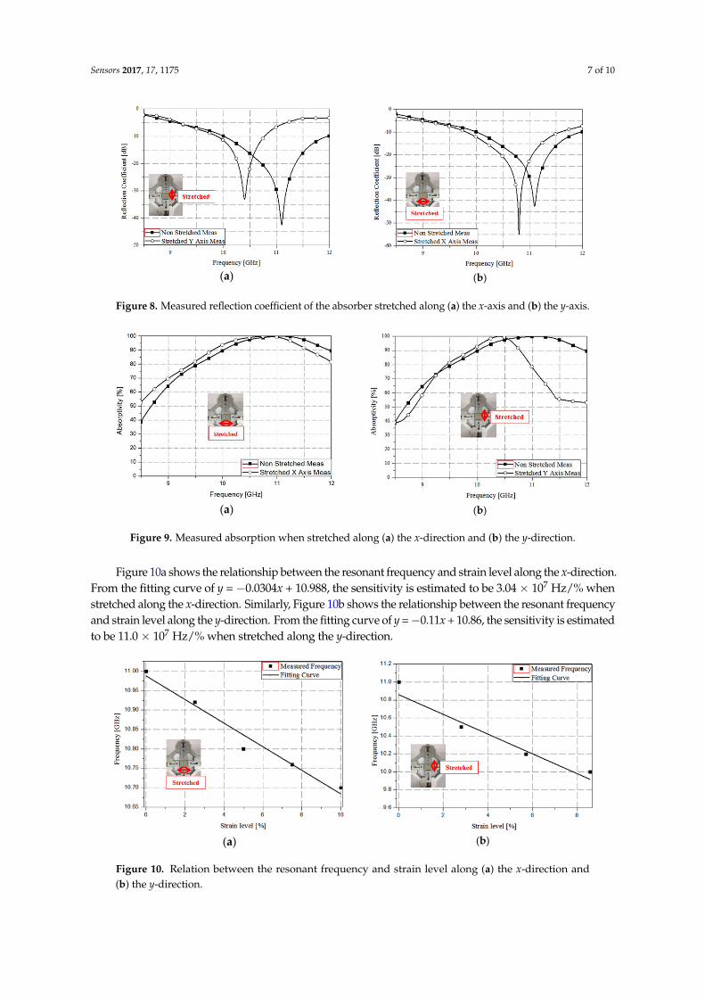
Sensors 2017, 17, 1175 7 of 10Sensors 2017, 17, x FOR PEER REVIEW 7 of 10
(a)
(b)
Figure 8. Measured reflection coefficient of the absorber stretched along (a) the x-axis and (b) the
y-axis.
(a)
(b)
Figure 9. Measured absorption when stretched along (a) the x-direction and (b) the y-direction.
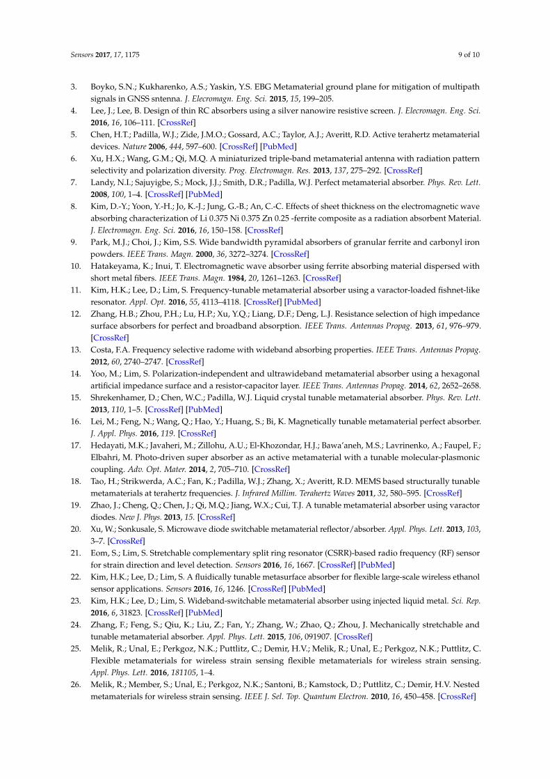
Figure 10a shows the relationship between the resonant frequency and strain level along the
x-direction. From the fitting curve of y = −0.0304x + 10.988, the sensitivity is estimated to be 3.04 ×
107 Hz/% when stretched along the x-direction. Similarly, Figure 10b shows the relationship
between the resonant frequency and strain level along the y-direction. From the fitting curve of y =
−0.11x + 10.86, the sensitivity is estimated to be 11.0 × 10⁷ Hz/% when stretched along the
y-direction.
(a)
(b)
Figure 10. Relation between the resonant frequency and strain level along (a) the x-direction and (b)
the y-direction.
Figure 8. Measured reflection coefficient of the absorber stretched along (a) the x-axis and (b) the y-axis.
Sensors 2017, 17, x FOR PEER REVIEW 7 of 10
(a)
(b)
Figure 8. Measured reflection coefficient of the absorber stretched along (a) the x-axis and (b) the
y-axis.
(a)
(b)
Figure 9. Measured absorption when stretched along (a) the x-direction and (b) the y-direction.
Figure 10a shows the relationship between the resonant frequency and strain level along the
x-direction. From the fitting curve of y = −0.0304x + 10.988, the sensitivity is estimated to be 3.04 ×
107 Hz/% when stretched along the x-direction. Similarly, Figure 10b shows the relationship
between the resonant frequency and strain level along the y-direction. From the fitting curve of y =
−0.11x + 10.86, the sensitivity is estimated to be 11.0 × 10⁷ Hz/% when stretched along the
y-direction.
(a)
(b)
Figure 10. Relation between the resonant frequency and strain level along (a) the x-direction and (b)
the y-direction.
Figure 9. Measured absorption when stretched along (a) the x-direction and (b) the y-direction.
Figure 10a shows the relationship between the resonant frequency and strain level along the x-direction.From the fitting curve of y =−0.0304x + 10.988, the sensitivity is estimated to be 3.04× 10⁷ Hz/% whenstretched along the x-direction. Similarly, Figure 10b shows the relationship between the resonant frequencyand strain level along the y-direction. From the fitting curve of y =−0.11x + 10.86, the sensitivity is estimatedto be 11.0× 10⁷ Hz/% when stretched along the y-direction.
Sensors 2017, 17, x FOR PEER REVIEW 7 of 10
(a)
(b)
Figure 8. Measured reflection coefficient of the absorber stretched along (a) the x-axis and (b) the
y-axis.
(a)
(b)
Figure 9. Measured absorption when stretched along (a) the x-direction and (b) the y-direction.
Figure 10a shows the relationship between the resonant frequency and strain level along the
x-direction. From the fitting curve of y = −0.0304x + 10.988, the sensitivity is estimated to be 3.04 ×
107 Hz/% when stretched along the x-direction. Similarly, Figure 10b shows the relationship
between the resonant frequency and strain level along the y-direction. From the fitting curve of y =
−0.11x + 10.86, the sensitivity is estimated to be 11.0 × 10⁷ Hz/% when stretched along the
y-direction.
(a)
(b)
Figure 10. Relation between the resonant frequency and strain level along (a) the x-direction and (b)
the y-direction. Figure 10. Relation between the resonant frequency and strain level along (a) the x-direction and(b) the y-direction.

Sensors 2017, 17, 1175 8 of 10
Figure 11a shows the measured reflection coefficients after 1, 5, 10, 20, and 30 cycles in order toprove adhesive strength and reliability. One cycle is defined as the un-stretched state after stretchingthe absorber. It is observed from Figure 11a that the resonant frequency is changed after 20 cycles.In addition, we measured a sheet resistance at different strain levels. As shown in Figure 11b,the resistances are 0.4, 0.6, 0.7, 1.0, 2.4, and 5.6 Ω when strain levels are 0%, 2%, 4%, 6%, 8%,and 10%, respectively.
Sensors 2017, 17, x FOR PEER REVIEW 8 of 10
Figure 11a shows the measured reflection coefficients after 1, 5, 10, 20, and 30 cycles in order to prove adhesive strength and reliability. One cycle is defined as the un-stretched state after stretching the absorber. It is observed from Figure 11a that the resonant frequency is changed after 20 cycles. In addition, we measured a sheet resistance at different strain levels. As shown in Figure 11b, the resistances are 0.4, 0.6, 0.7, 1.0, 2.4, and 5.6 Ω when strain levels are 0%, 2%, 4%, 6%, 8%, and 10%, respectively.
(a) (b)
Figure 11. (a) Measured reflection coefficients after stretching for 30 cycles and (b) measured resistivity at different strain levels from 0 to 10%.
5. Conclusions
In this paper, we proposed a stretchable electromagnetic absorber fabricated using screen printing technology. In order to realize stretchable characteristics in screen printing technology, a stretchable PDMS material and PE872 stretchable conductive ink were used as the substrate and conductor, respectively. Two rectangular patch unit cells of dimensions 8 mm × 7 mm were printed on top of the PDMS substrate. We measured the performance of the screen-printed electromagnetic absorber using a network analyzer and a WR-90 waveguide. The resonant frequency was determined to be 11 GHz with a reflection coefficient of −33 dB. When the length of the absorber was increased along the y-direction, the resonant frequency decreased by 0.6 GHz, from 11 to 10.4 GHz, demonstrating 99% absorption. When the length of the absorber was increased along the x-direction, the resonance frequency decreased by 0.3 GHz, from 11.1 to 10.8 GHz. Therefore, we demonstrated the successful fabrication of a stretchable electromagnetic absorber by using screen printing technology and validated the results through simulation and experiment. For practical applications, the screen-printed patterns must be encapsulated in order to protect from moisture permeation or damages.
Acknowledgments: This work has been supported by the Low Observable Technology Research Center program of Defense Acquisition Program Administration and Agency for Defense Development.
Author Contributions: Heijun Jeong designed, analyzed, fabricated, and measured the sample. Sungjoon Lim conceived the idea and contributed to the revision of the manuscript.
Conflicts of Interest: The authors declare no conflict of interest.
References
1. Schurig, D.; Mock, J.J.; Justice, B.J.; Cummer, S.A.; Pendry, J.B.; Starr, A.F.; Smith, D.R. Metamaterial electromagnetic cloak at microwave frequencies. Science 2006, 314, 977–980.
2. Newsome, W.T.; Goldberg, M.E.; Maunsell, J.H.R.; Buneo, C.A.; Duncan, J.; Cave, K.R.; Franzel, S.L.; Miller, E.K.; Duncan, J.; Desimone, R.; et al. Sub-diffraction-limited optical imaging with a silver superlens. Science 2005, 1783, 534–537.
Figure 11. (a) Measured reflection coefficients after stretching for 30 cycles and (b) measured resistivityat different strain levels from 0 to 10%.
5. Conclusions
In this paper, we proposed a stretchable electromagnetic absorber fabricated using screen printingtechnology. In order to realize stretchable characteristics in screen printing technology, a stretchablePDMS material and PE872 stretchable conductive ink were used as the substrate and conductor,respectively. Two rectangular patch unit cells of dimensions 8 mm × 7 mm were printed on top ofthe PDMS substrate. We measured the performance of the screen-printed electromagnetic absorberusing a network analyzer and a WR-90 waveguide. The resonant frequency was determined to be11 GHz with a reflection coefficient of −33 dB. When the length of the absorber was increased alongthe y-direction, the resonant frequency decreased by 0.6 GHz, from 11 to 10.4 GHz, demonstrating99% absorption. When the length of the absorber was increased along the x-direction, the resonancefrequency decreased by 0.3 GHz, from 11.1 to 10.8 GHz. Therefore, we demonstrated the successfulfabrication of a stretchable electromagnetic absorber by using screen printing technology and validatedthe results through simulation and experiment. For practical applications, the screen-printed patternsmust be encapsulated in order to protect from moisture permeation or damages.
Acknowledgments: This work has been supported by the Low Observable Technology Research Center programof Defense Acquisition Program Administration and Agency for Defense Development.
Author Contributions: Heijun Jeong designed, analyzed, fabricated, and measured the sample. Sungjoon Limconceived the idea and contributed to the revision of the manuscript.
Conflicts of Interest: The authors declare no conflict of interest.
References
1. Schurig, D.; Mock, J.J.; Justice, B.J.; Cummer, S.A.; Pendry, J.B.; Starr, A.F.; Smith, D.R. Metamaterialelectromagnetic cloak at microwave frequencies. Science 2006, 314, 977–980. [CrossRef] [PubMed]
2. Newsome, W.T.; Goldberg, M.E.; Maunsell, J.H.R.; Buneo, C.A.; Duncan, J.; Cave, K.R.; Franzel, S.L.;Miller, E.K.; Duncan, J.; Desimone, R.; et al. Sub-diffraction-limited optical imaging with a silver superlens.Science 2005, 1783, 534–537.
Sensors 2017, 17, 1175 9 of 10
3. Boyko, S.N.; Kukharenko, A.S.; Yaskin, Y.S. EBG Metamaterial ground plane for mitigation of multipathsignals in GNSS sntenna. J. Elecromagn. Eng. Sci. 2015, 15, 199–205.
4. Lee, J.; Lee, B. Design of thin RC absorbers using a silver nanowire resistive screen. J. Elecromagn. Eng. Sci.2016, 16, 106–111. [CrossRef]
5. Chen, H.T.; Padilla, W.J.; Zide, J.M.O.; Gossard, A.C.; Taylor, A.J.; Averitt, R.D. Active terahertz metamaterialdevices. Nature 2006, 444, 597–600. [CrossRef] [PubMed]
6. Xu, H.X.; Wang, G.M.; Qi, M.Q. A miniaturized triple-band metamaterial antenna with radiation patternselectivity and polarization diversity. Prog. Electromagn. Res. 2013, 137, 275–292. [CrossRef]
7. Landy, N.I.; Sajuyigbe, S.; Mock, J.J.; Smith, D.R.; Padilla, W.J. Perfect metamaterial absorber. Phys. Rev. Lett.2008, 100, 1–4. [CrossRef] [PubMed]
8. Kim, D.-Y.; Yoon, Y.-H.; Jo, K.-J.; Jung, G.-B.; An, C.-C. Effects of sheet thickness on the electromagnetic waveabsorbing characterization of Li 0.375 Ni 0.375 Zn 0.25 -ferrite composite as a radiation absorbent Material.J. Electromagn. Eng. Sci. 2016, 16, 150–158. [CrossRef]
9. Park, M.J.; Choi, J.; Kim, S.S. Wide bandwidth pyramidal absorbers of granular ferrite and carbonyl ironpowders. IEEE Trans. Magn. 2000, 36, 3272–3274. [CrossRef]
10. Hatakeyama, K.; Inui, T. Electromagnetic wave absorber using ferrite absorbing material dispersed withshort metal fibers. IEEE Trans. Magn. 1984, 20, 1261–1263. [CrossRef]
11. Kim, H.K.; Lee, D.; Lim, S. Frequency-tunable metamaterial absorber using a varactor-loaded fishnet-likeresonator. Appl. Opt. 2016, 55, 4113–4118. [CrossRef] [PubMed]
12. Zhang, H.B.; Zhou, P.H.; Lu, H.P.; Xu, Y.Q.; Liang, D.F.; Deng, L.J. Resistance selection of high impedancesurface absorbers for perfect and broadband absorption. IEEE Trans. Antennas Propag. 2013, 61, 976–979.[CrossRef]
13. Costa, F.A. Frequency selective radome with wideband absorbing properties. IEEE Trans. Antennas Propag.2012, 60, 2740–2747. [CrossRef]
14. Yoo, M.; Lim, S. Polarization-independent and ultrawideband metamaterial absorber using a hexagonalartificial impedance surface and a resistor-capacitor layer. IEEE Trans. Antennas Propag. 2014, 62, 2652–2658.
15. Shrekenhamer, D.; Chen, W.C.; Padilla, W.J. Liquid crystal tunable metamaterial absorber. Phys. Rev. Lett.2013, 110, 1–5. [CrossRef] [PubMed]
16. Lei, M.; Feng, N.; Wang, Q.; Hao, Y.; Huang, S.; Bi, K. Magnetically tunable metamaterial perfect absorber.J. Appl. Phys. 2016, 119. [CrossRef]
17. Hedayati, M.K.; Javaheri, M.; Zillohu, A.U.; El-Khozondar, H.J.; Bawa’aneh, M.S.; Lavrinenko, A.; Faupel, F.;Elbahri, M. Photo-driven super absorber as an active metamaterial with a tunable molecular-plasmoniccoupling. Adv. Opt. Mater. 2014, 2, 705–710. [CrossRef]
18. Tao, H.; Strikwerda, A.C.; Fan, K.; Padilla, W.J.; Zhang, X.; Averitt, R.D. MEMS based structurally tunablemetamaterials at terahertz frequencies. J. Infrared Millim. Terahertz Waves 2011, 32, 580–595. [CrossRef]
19. Zhao, J.; Cheng, Q.; Chen, J.; Qi, M.Q.; Jiang, W.X.; Cui, T.J. A tunable metamaterial absorber using varactordiodes. New J. Phys. 2013, 15. [CrossRef]
20. Xu, W.; Sonkusale, S. Microwave diode switchable metamaterial reflector/absorber. Appl. Phys. Lett. 2013, 103,3–7. [CrossRef]
21. Eom, S.; Lim, S. Stretchable complementary split ring resonator (CSRR)-based radio frequency (RF) sensorfor strain direction and level detection. Sensors 2016, 16, 1667. [CrossRef] [PubMed]
22. Kim, H.K.; Lee, D.; Lim, S. A fluidically tunable metasurface absorber for flexible large-scale wireless ethanolsensor applications. Sensors 2016, 16, 1246. [CrossRef] [PubMed]
23. Kim, H.K.; Lee, D.; Lim, S. Wideband-switchable metamaterial absorber using injected liquid metal. Sci. Rep.2016, 6, 31823. [CrossRef] [PubMed]
24. Zhang, F.; Feng, S.; Qiu, K.; Liu, Z.; Fan, Y.; Zhang, W.; Zhao, Q.; Zhou, J. Mechanically stretchable andtunable metamaterial absorber. Appl. Phys. Lett. 2015, 106, 091907. [CrossRef]
25. Melik, R.; Unal, E.; Perkgoz, N.K.; Puttlitz, C.; Demir, H.V.; Melik, R.; Unal, E.; Perkgoz, N.K.; Puttlitz, C.Flexible metamaterials for wireless strain sensing flexible metamaterials for wireless strain sensing.Appl. Phys. Lett. 2016, 181105, 1–4.
26. Melik, R.; Member, S.; Unal, E.; Perkgoz, N.K.; Santoni, B.; Kamstock, D.; Puttlitz, C.; Demir, H.V. Nestedmetamaterials for wireless strain sensing. IEEE J. Sel. Top. Quantum Electron. 2010, 16, 450–458. [CrossRef]

Sensors 2017, 17, 1175 10 of 10
27. Surapaneni, R.; Xie, Y.; Park, K.; Mastrangelo, C. Microfabrication of flexible self-repairing ground reactionsensor with liquid metal electrodes. Procedia Eng. 2011, 25, 124–127. [CrossRef]
28. Amjadi, M.; Park, I. Carbon nanotubes-ecoflex nanocomposite for strain sensing with ultra-high stretchability.In Proceedings of the 28th IEEE International Conference on Micro Electro Mechanical Systems (MEMS),Estoril, Portugal, 18–22 January 2015; pp. 744–747.
29. San-Miguel, A.; Lu, H. Microfluidics as a tool for C. elegans research. WormBook 2013. [CrossRef] [PubMed]30. Li, X.; Abe, T.; Esashi, M. Deep reactive ion etching of Pyrex glass using SF6 plasma. Sens. Actuators A Phys.
2001, 87, 139–145. [CrossRef]31. Garg, B.; Verma, R.D.; Samadhiya, A. Design of rectangular microstrip patch antenna incorporated with
innovative metamaterial structure for dual band operation and amelioration in patch antenna parameterswith negative µ and ε. Int. J. Eng. Technol. 2012, 1, 205–216. [CrossRef]
32. Peterson, R.L.; Drayton, R.F. A CPW T-resonator technique for electrical characterization of microwavesubstrates. In Proceedings of the 57th IEEE ARFTG Conference, Phoenix, AZ, USA, 25–25 May 2001.[CrossRef]
33. Lätti, K.P.; Kettunen, M.; Strom, J.P.; Silventoinen, P. A review of microstrip T-resonator method indetermining the dielectric properties of printed circuit board materials. IEEE Trans. Instrum. Meas. 2007, 56,1845–1850. [CrossRef]
34. Khondoker, M.A.H.; Sameoto, D. Fabrication methods and applications of microstructured gallium basedliquid metal alloys. Smart Mater. Struct. 2016, 25, 093001. [CrossRef]
35. Fallahzadeh, S.; Forooraghi, K.; Atlasbaf, Z. A polarization-insensitive metamaterial absorber with a broadangular band. In Proceedings of the 20th IEEE Electrical Engineering (ICEE), Tehran, Iran, 15–17 May 2012.[CrossRef]
36. Tak, J.; Lee, Y.; Choi, J. Design of a metamaterial absorber for ISM applications. J. Elecromagn. Eng. Sci.2013, 13, 1–7. [CrossRef]
37. Kamei, K.; Mashimo, Y.; Koyama, Y.; Fockenberg, C.; Nakashima, M.; Nakajima, M.; Li, J.; Chen, Y.3D printing of soft lithography mold for rapid production of polydimethylsiloxane-based microfluidicdevices for cell stimulation with concentration gradients. Biomed. Microdevices 2015, 17. [CrossRef] [PubMed]
38. Kubo, M.; Li, X.; Kim, C.; Hashimoto, M.; Wiley, B.J.; Ham, D.; Whitesides, G.M. Stretchable microfluidicradiofrequency antennas. Adv. Mater. 2010, 22, 2749–2752. [CrossRef] [PubMed]
39. Li, C.-Y.; Liao, Y.-C. Adhesive stretchable printed conductive thin film patterns on PDMS surface withan atmospheric plasma treatment. ACS Appl. Mater. Interfaces 2016, 8, 11868–11874. [CrossRef] [PubMed]
40. Auyeung, R.C.Y.; Kim, H.; Mathews, S.A.; Piqué, A. Laser direct-write of metallic nanoparticle inks. J. LaserMicro Nanoeng. 2007, 2, 21–25. [CrossRef]
© 2017 by the authors. Licensee MDPI, Basel, Switzerland. This article is an open accessarticle distributed under the terms and conditions of the Creative Commons Attribution(CC BY) license (http://creativecommons.org/licenses/by/4.0/).