
A strain or electric field induced direct bandgap in ... · the VASP package.46 Projector augmented...
7
7156 | Phys. Chem. Chem. Phys., 2016, 18, 7156--7162 This journal is © the Owner Societies 2016 Cite this: Phys. Chem. Chem. Phys., 2016, 18, 7156 A strain or electric field induced direct bandgap in ultrathin silicon film and its application in photovoltaics or photocatalysis† Tengfei Cao, a Da Wang, a Dong-Sheng Geng, a Li-Min Liu* a and Jijun Zhao* ab The indirect bandgap character of silicon greatly limits its applications in electronic or optoelectronic devices, and direct bandgaps are highly desirable in all silicon allotropes. The successful synthesis of ultrathin or even monolayer silicon films experimentally has opened new opportunities to further modulate the electronic structure of silicon through external modulation. In this work, strain or electric field effects on the electronic structure of ultrathin silicon film (USF) are systematically explored. The results demonstrate that all USFs are indirect band-gap semiconductors; interestingly, tensile strain or electric field efficiently tunes the USFs into direct band gap semiconductors. The indirect to direct band gap transition in the USFs not only extends their light adsorption spectra into the visible light region but also greatly enhances the adsorption intensity. Because of this, strained USFs have great potential to be used as a high-performance photovoltaic material. Furthermore, the high stability, moderate band-gap and proper band edge positions demonstrate that monolayer and bilayer USFs can also be used as photocatalysts for water splitting. 1. Introduction Silicon, an essential component of modern semiconductor technology, is quite abundant in the Earth’s crust. In nature, silicon exists in various oxygen-rich minerals, and purified silicon mainly takes on a cubic diamond structure, which is one kind of indirect band-gap semiconductor. The direct bandgap of cubic Si (3.2 eV) is much wider than the indirect one (1.17 eV), 1,2 and thus phonons are needed to mediate electronic excitations from the valence band maximum (VBM) to the conduction band minimum (CBM). Moreover, in bulk states, electronic structure modulations in silicon are relatively difficult because of its closely packed configuration and strong covalent Si–Si bonds. All of these prevent the application of silicon in high performance photovoltaic or photocatalytic devices, where a direct bandgap is highly desirable. Nanoprocessing is an efficient way to achieve chemical activity of silicon and to achieve different silicon allotropes with direct band-gaps. 3–8 For example, when bulk silicon is processed into clusters or nanowires, its electronic structure becomes efficiently modulated by atom decoration, strain or electric field and direct moderate band-gaps can be easily achieved. 5,9,10 Moreover, inspired by the successful synthesis of graphene experimentally, 11–15 ultrathin two dimensional (2D) nanomaterials have drawn more and more attention. 16–18 For example, 2D hexagonal boron nitrides (h-BN) 19–23 and transition metal sulfides (selenide) 24–28 have been synthesized and exhibit novel electronic or magnetic properties not comparable to their bulk states. For silicon, even though these are no graphite-like layer phases in its bulk state, its monolayer structure with honeycomb geometry (silicene) has been successfully synthesized experimentally on Ag(111), 29–31 Ir(111), 32 and ZrB2(0001) 33 surfaces. Theoretical analysis demonstrates that the electronic properties of freestanding silicene are quite similar to those of graphene. Furthermore, multi- layer silicenes (MLS) exhibit properties totally different from the monolayer structure and also draw intense attention. 34–36 Theoretically, MLS can adopt different stacking patterns, AB..., ABC..., AA..., slide AA... and so on. Among them, ABA... and ABC... stacking structures are among the most stable patterns, especially when the included layer number becomes relatively large. Combining first principles simulation and scanning tunnelling microscopy detection, Li and Meng et al. demonstrated that MLS on Ag(111) spontaneously transformed into diamond- like bulk Si films without any reconstruction observed in the silicon(111) surface. 35 Wu et al. further demonstrated that MLS films (MLS-F) exhibit stable ABC-stacking configurations, and because of the surface states, these MLS-Fs exhibit metallic character. 36 a Beijing Computational Science Research Center, Beijing 100084, China. E-mail: [email protected] b Key Laboratory of Materials Modification by Laser, Ion and Electron Beams, Dalian University of Technology, Ministry of Education, Dalian 116024, China. E-mail: [email protected] † Electronic supplementary information (ESI) available. See DOI: 10.1039/c5cp06528c Received 27th October 2015, Accepted 26th January 2016 DOI: 10.1039/c5cp06528c www.rsc.org/pccp PCCP PAPER Published on 27 January 2016. Downloaded by Beijing University on 23/07/2016 08:03:20. View Article Online View Journal | View Issue
Transcript of A strain or electric field induced direct bandgap in ... · the VASP package.46 Projector augmented...
7156 | Phys. Chem. Chem. Phys., 2016, 18, 7156--7162 This journal is© the Owner Societies 2016
Cite this:Phys.Chem.Chem.Phys.,
2016, 18, 7156
A strain or electric field induced direct bandgap inultrathin silicon film and its application inphotovoltaics or photocatalysis†
Tengfei Cao,a Da Wang,a Dong-Sheng Geng,a Li-Min Liu*a and Jijun Zhao*ab
The indirect bandgap character of silicon greatly limits its applications in electronic or optoelectronic
devices, and direct bandgaps are highly desirable in all silicon allotropes. The successful synthesis of
ultrathin or even monolayer silicon films experimentally has opened new opportunities to further
modulate the electronic structure of silicon through external modulation. In this work, strain or electric
field effects on the electronic structure of ultrathin silicon film (USF) are systematically explored. The
results demonstrate that all USFs are indirect band-gap semiconductors; interestingly, tensile strain or
electric field efficiently tunes the USFs into direct band gap semiconductors. The indirect to direct band
gap transition in the USFs not only extends their light adsorption spectra into the visible light region but
also greatly enhances the adsorption intensity. Because of this, strained USFs have great potential to be
used as a high-performance photovoltaic material. Furthermore, the high stability, moderate band-gap
and proper band edge positions demonstrate that monolayer and bilayer USFs can also be used as
photocatalysts for water splitting.
1. Introduction
Silicon, an essential component of modern semiconductortechnology, is quite abundant in the Earth’s crust. In nature,silicon exists in various oxygen-rich minerals, and purifiedsilicon mainly takes on a cubic diamond structure, which isone kind of indirect band-gap semiconductor. The direct bandgapof cubic Si (3.2 eV) is much wider than the indirect one (1.17 eV),1,2
and thus phonons are needed to mediate electronic excitationsfrom the valence band maximum (VBM) to the conduction bandminimum (CBM). Moreover, in bulk states, electronic structuremodulations in silicon are relatively difficult because of its closelypacked configuration and strong covalent Si–Si bonds. All ofthese prevent the application of silicon in high performancephotovoltaic or photocatalytic devices, where a direct bandgap ishighly desirable.
Nanoprocessing is an efficient way to achieve chemical activityof silicon and to achieve different silicon allotropes with directband-gaps.3–8 For example, when bulk silicon is processed intoclusters or nanowires, its electronic structure becomes efficiently
modulated by atom decoration, strain or electric field and directmoderate band-gaps can be easily achieved.5,9,10 Moreover, inspiredby the successful synthesis of graphene experimentally,11–15
ultrathin two dimensional (2D) nanomaterials have drawnmore and more attention.16–18 For example, 2D hexagonal boronnitrides (h-BN)19–23 and transition metal sulfides (selenide)24–28
have been synthesized and exhibit novel electronic or magneticproperties not comparable to their bulk states.
For silicon, even though these are no graphite-like layer phasesin its bulk state, its monolayer structure with honeycomb geometry(silicene) has been successfully synthesized experimentally onAg(111),29–31 Ir(111),32 and ZrB2(0001)33 surfaces. Theoreticalanalysis demonstrates that the electronic properties of freestandingsilicene are quite similar to those of graphene. Furthermore, multi-layer silicenes (MLS) exhibit properties totally different fromthe monolayer structure and also draw intense attention.34–36
Theoretically, MLS can adopt different stacking patterns, AB. . .,ABC. . ., AA. . ., slide AA. . . and so on. Among them, ABA. . . andABC. . . stacking structures are among the most stable patterns,especially when the included layer number becomes relativelylarge. Combining first principles simulation and scanningtunnelling microscopy detection, Li and Meng et al. demonstratedthat MLS on Ag(111) spontaneously transformed into diamond-like bulk Si films without any reconstruction observed in thesilicon(111) surface.35 Wu et al. further demonstrated that MLS films(MLS-F) exhibit stable ABC-stacking configurations, and because ofthe surface states, these MLS-Fs exhibit metallic character.36
a Beijing Computational Science Research Center, Beijing 100084, China.
E-mail: [email protected] Key Laboratory of Materials Modification by Laser, Ion and Electron Beams,
Dalian University of Technology, Ministry of Education, Dalian 116024, China.
E-mail: [email protected]
† Electronic supplementary information (ESI) available. See DOI: 10.1039/c5cp06528c
Received 27th October 2015,Accepted 26th January 2016
DOI: 10.1039/c5cp06528c
www.rsc.org/pccp
PCCP
PAPER
Publ
ishe
d on
27
Janu
ary
2016
. Dow
nloa
ded
by B
eijin
g U
nive
rsity
on
23/0
7/20
16 0
8:03
:20.
View Article OnlineView Journal | View Issue

This journal is© the Owner Societies 2016 Phys. Chem. Chem. Phys., 2016, 18, 7156--7162 | 7157
The successful synthesis of MLS-Fs experimentally not onlyenriches the nanoscale states of silicon, but also greatly extendsits electronic structural diversity and broadens its potentialapplications. Moreover, in the MLS-Fs, the reduced dimensionsgreatly increase the surface ratio with respect to volume, whichprovides plenty of reaction sites for catalytic reactions, and thequantum confinement effects in MLS-Fs make their responseto external modulations totally different from that of bulksilicon. Hence, to make full use of these MLS-Fs in electronicor optoelectronic devices, it is of essential importance to knowtheir stability and intrinsic electronic structure, as well as theirresponse to external modulations.
Strain, electric field and small atom decoration are usuallyadopted to tailor the electronic structures of low dimensionalsystems because of their easy application and considerablemodulation effects.10,37–43 For example, with the applicationof in-plane strain, the magnetic states of the transition metalsulfides (or oxides) can be efficiently modulated.43,44 An electricfield not only efficiently alters the band gaps, but also theanisotropic carrier mobility of multilayer black phosphorus.45
However, contrary to the extensive studies on these layered 2Dsemiconductors, research on the strain or electric field effectsof MLS-Fs is relatively insufficient, which is also not compatiblewith the thorough studies on bulk silicon and mature silicontechnology in the modern semiconductor industry.
In this work, based on experimental observations, ultrathinsilicon films derived from AB-stacked bilayer and ABC-stackedmultilayer silicenes are reported. For comparison, silicon filmsin other orientations are shown in Fig. S2 (ESI†). Hydrogen isapplied to saturate all surface dangling bonds. The strain orelectric field dependent electronic structures and light adsorptionspectra as well as the potential applications of the USFs inphotovoltaic or photocatalytic materials are systematically studied.All USFs are indirect band gap semiconductors with the gapmagnitude being determined by the total number of siliconlayers. Upon applying tensile strain or an electric field, the bandgaps of the USFs are efficiently reduced, and indirect–directbandgap transitions occur under a certain strain or field magnitude.Because of the tensile strain induced bandgap reduction andindirect–direct bandgap transitions, the light adsorption spectra ofUSFs are extended to the visible light range and the adsorptionintensity is greatly enhanced. Moreover, under tensile strain,one layer and bilayer silicon films can be used as photocatalyticmaterials because of their moderate bandgaps and properenergy levels of the CBM and VBM.
2. Methods
All electronic structure calculations were performed within thedensity functional theory (DFT) formalism as implemented inthe VASP package.46 Projector augmented wave (PAW) methodswere used to describe electron–ion interactions.47 Exchangeand correlation interactions were calculated using the Perdew,Burke and Ernzerhof (PBE) method within the generalized gradientapproximation (GGA). The more accurate Heyd–Scuseria–Ernzerhof
(HSE06) hybrid functional48 was used to determine the energylevels of the VBM, the CBM and the band-gaps. The electronwave function and charge density were expanded in planewaves, and the energy cutoff for the plane waves was 500 eV.The corresponding Brillouin zone was sampled in a 18 � 18 � 1mesh within the Monkhorst–Pack scheme.
All structures were fully optimized within a force thresholdof 0.01 eV Å�1. The Methfessel–Paxton smearing technique witha width of 0.02 eV was used to speed up the convergence. Theadsorption energy was used to determine the static stabilityof hydrogens on silicon, which was obtained as: Ead = 1/n �(EUSF � Esif � n � mH), where EUSF, Esif and mH are the energy ofsilicon film with hydrogen adsorption, the silicon film with nohydrogen and the chemical potential of molecular hydrogen,respectively, and n is the total number of hydrogen atoms.Moreover, the phonon spectrum computed with the densityfunction perturbation theory (DFPT) was used to prove thedynamical stability of USFs. In-plane tensile strain was appliedthrough a lattice extension and the strain rate was defined as(ax � a0)/a0, where ax and a0 are the lattice constants of thestrained silicon and the unstrained one, respectively.
Based on the electronic structure (HSE06 level), light adsorptionspectra were calculated within the random phase approximation(RPA).49 In the first step, the frequency dependent dielectric matrixwas calculated. The imaginary part is determined by a summationover empty states using the equation:
eimaab ðoÞ ¼
4p2e2
Olimq!0
1
q2
Xc;v;k
2okd eck � evk � oð Þ
� mckþeaq j mvk� ��
mvkþebq j mvk�� (1)
The indices c and v refer to conduction and valence band statesrespectively, and mck is the cell periodic part of the wave function at
the k-point k. The real part is: erealab ðoÞ ¼ 1þ 2
pPÐ10
eimaab ðo0Þo0
o02 � o2 þ iZdo0,
where P is the principle value and Z is the complex shift. Upon thecalculated dielectric matrix, the light adsorption intensity wascalculated using the following equations:
aðoÞ ¼ eimaðoÞ � onðoÞ � c
(2)
where c is the speed of light and
nðoÞ ¼
ffiffiffiffiffiffiffiffiffiffiffiffiffiffiffiffiffiffiffiffiffiffiffiffiffiffiffiffiffiffiffiffiffiffiffiffiffiffiffiffiffiffiffiffiffiffiffiffiffiffiffiffiffiffiffiffiffiffiffiffiffiffiffiffiffierealðoÞ þ
ffiffiffiffiffiffiffiffiffiffiffiffiffiffiffiffiffiffiffiffiffiffiffiffiffiffiffiffiffiffiffiffiffiffiffiffiffiffiffierealðoÞ2 þ eimaðoÞ2
p2
s.
The finite homogeneous electric field e was applied withthe modern theory of polarization.50 The field-polarized Blochfunctions c(e) were obtained by minimizing the electricenthalpy functional: E{c(e),e} = E0[{c(e)}] � O � e � P[{c(e)}],where P[{c(e)}] is the macroscopic polarization. Upon applyingthe electric field, long range interactions between the USF andits neighbor images will be induced. To exclude such longrange interactions, a vacuum as large as 40 Å was adopted.
Paper PCCP
Publ
ishe
d on
27
Janu
ary
2016
. Dow
nloa
ded
by B
eijin
g U
nive
rsity
on
23/0
7/20
16 0
8:03
:20.
View Article Online
7158 | Phys. Chem. Chem. Phys., 2016, 18, 7156--7162 This journal is© the Owner Societies 2016
3. Results and discussion
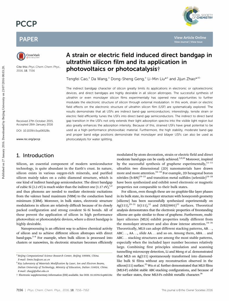
The structures of the USFs are given in Fig. 1. Monolayer USF isfully hydrogenated silicon. Bilayer and multilayer configurationsare obtained from the AB and ABC-stacked MLSs, which have beenproven to be stable in ultrathin silicon films. Moreover, consistentwith Wu et al.,36 we found that interlayer bonds can automaticallyform in MLSs (see Fig. S1, ESI†), which breaks the p bonds of theoutermost silicene layers, and induces dangling-bond surfacestates in these silicon films (see Fig. S1(h and i), ESI†). Thesedangling-bond states just pass through the Fermi level andcontribute to the metallic character of these thin films. Hydrogensare applied to saturate these surface dangling states. The adsorptionenergy demonstrates that the adsorption of hydrogen atoms onsilicon films is favorable, because these unfilled bond states provideadsorption sites for the hydrogen atoms.51 The results in Fig. 1(b–d)demonstrate that all these USFs are semiconductors because ofhydrogen decoration. Such a phenomenon is different from themultilayer silicene, which may be semiconductor or metaldependent on the stacking patterns.34
Moreover, all these USFs have indirect band gap electronicstructures with a VBM at the G point and a CBM located at aroundM (see Fig. 1(b)). Because of quantum confinement effects,52
monolayer USF exhibits the largest direct (3.14 eV) and indirect(2.94 eV) band gaps, but the energy difference between them issmall (0.2 eV). These values are consistent with those of othertheoretical work.53 With an increase in silicon layer number, bothdirect and indirect band gaps of USFs gradually reduce, but theenergy difference between them becomes relatively large. Forexample, five-layer USF exhibits a band gap of 2.19 and 1.41 eVfor the direct and indirect one, respectively. But the energydifference between them is 0.78 eV. All these observations resultfrom the fact that, with the increase of the silicon layer number,the electronic structure of multilayer silicon gradually approaches
that of bulk silicon. The projected density of states (PDOS) of five-layer USFs (see Fig. 1(d)) demonstrates that the VBM and CBMaround the Fermi level are thoroughly contributed to by the 3pstates of silicon atoms. Hence, hydrogen adsorption only saturatesthe surface dangling bonds and the electronic properties of USFsare mainly determined by the states of silicon atoms.
Compared with the bulk states (2.03 eV), the energy differencebetween the direct and indirect band-gap in USFs is relativelysmall. It provides more possibilities to achieve direct band gaps inUSFs through external modulation. In practice, strain and electricfield are widely used to tailor the electronic structures of materials,especially of low dimensional systems. Both of them are alsounavoidable in optoelectronic or electronic devices because ofthe electronic potential difference between different atoms andthe lattice mismatch between different materials. In the end, toachieve direct bandgaps in USFs, strain or electric field effectson the electronic structures of USFs are systematically explored.
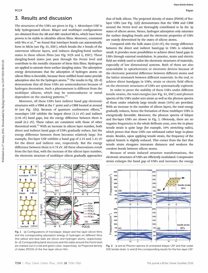
In order to prove the stability of these USFs under differenttensile strains, the total energies (see Fig. S3, ESI†) and phononspectra of the USFs under zero strain as well as the phonon spectraof those under relatively large tensile strain (10%) are provided.With an increase in the number of silicon layers, the total energygradually reduces, hence the formation of these multilayer USFs isenergetically favorable. Moreover, the phonon spectra of bilayerand five-layer USFs are shown in Fig. 2. Obviously, there are nonegative frequencies in the whole Brillouin zone, even the in-planetensile strain is quite large (for example, 10% stretching radio),which proves that these USFs can withstand rather large in-planestrain. Besides, upon applying tensile strain, the frequency of theoptical branch is slightly reduced. This comes from the fact thattensile strain elongates interatom distances and weakens thecovalent bonds between silicon atoms.
Because of strain induced structure transformations, theelectronic structures of USFs are efficiently modulated. Compressivestrain enlarges the band gap of USFs and increases the energy
Fig. 1 (a) Configurations of monolayer, bilayer and five-layer silicon filmsand the corresponding adsorption energy of hydrogen on different films(the yellow and blue balls are silicon and hydrogen atoms, respectively).(b–d) Corresponding band structures and the states around the Fermi levelare marked out in a red and green color, respectively. (e) Projected densityof states (PDOS) of the five-layer silicon film.
Fig. 2 (a and b) Phonon spectra of unstrained bilayer USF and that under10% tensile strain; (c and d) the corresponding results for the five-layer USF.
PCCP Paper
Publ
ishe
d on
27
Janu
ary
2016
. Dow
nloa
ded
by B
eijin
g U
nive
rsity
on
23/0
7/20
16 0
8:03
:20.
View Article Online
This journal is© the Owner Societies 2016 Phys. Chem. Chem. Phys., 2016, 18, 7156--7162 | 7159
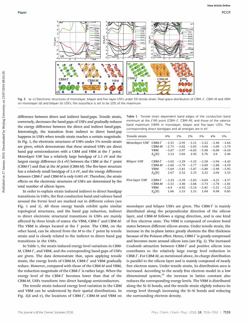
difference between direct and indirect band-gaps. Tensile strain,conversely, decreases the band-gaps of USFs and gradually reducesthe energy difference between the direct and indirect band-gaps.Interestingly, the transition from indirect to direct band-gaphappens in USFs when tensile strain reaches a certain magnitude.In Fig. 3, the electronic structures of USFs under 5% tensile strainare given, which demonstrate that these strained USFs are directband gap semiconductors with a CBM and VBM at the G point.Monolayer USF has a relatively large bandgap of 2.3 eV and thelargest energy difference (0.4 eV) between the CBM at the G point(CBM-G) and that at the M point (CBM-M). The five-layer structurehas a relatively small bandgap of 1.4 eV, and the energy differencebetween CBM-G and CBM-M is only 0.005 eV. Therefore, the straineffects on the electronic structures of USFs are determined by thetotal number of silicon layers.
In order to explain strain induced indirect to direct bandgaptransitions in USFs, the first conduction band and valence bandaround the Fermi level are marked out in different colors (seeFig. 1 and 3). All these energy bands exhibit quite similartopological structures, and the band gap reduction, indirectto direct electronic structural transitions in USFs are mainlyaffected by three kinds of states: the VBM, CBM-G and CBM-M.The VBM is always located at the G point. The CBM, on theother hand, can be altered from the M to the G point by tensilestrain and is closely related to the indirect to direct band gaptransitions in the USFs.
In Table 1, the strain induced energy level variations in CBM-M, CBM-G, and VBM, and the corresponding band-gaps of USFsare given. The data demonstrate that, upon applying tensilestrain, the energy levels of CBM-M, CBM-G and VBM graduallyreduce. However, compared with those of the CBM-M and VBM,the reduction magnitude of the CBM-G is rather large. When theenergy level of the CBM-G becomes lower than that of theCBM-M, USFs transform into direct bandgap semiconductors.
The tensile strain induced energy level variation in the CBMand VBM can be understood by their spatial distributions. InFig. 3(d and e), the locations of CBM-G, CBM-M and VBM on
monolayer and bilayer USFs are given. The CBM-G is mainlydistributed along the perpendicular direction of the siliconlayer, and CBM-M follows a zigzag direction, and is one kindof free electron state. The VBM is composed of covalent bondstates between different silicon atoms. Under tensile strain, theincrease in the in-plane lattice greatly shortens the film thicknessbecause of the Poisson effect. Hence, CBM-G is greatly compressedand becomes more around silicon ions (see Fig. 3). The increasedCoulomb attraction between CBM-G and positive silicon ionscontributes to the relatively large energy level reduction inCBM-G. For CBM-M, as mentioned above, its charge distributionis parallel to the silicon layer and is mainly composed of nearlyfree electron states. Under tensile strain, its distribution area isincreased. According to the nearly free electron model in a lowdimensional system,54 the increase in lattice constant alsoreduces the corresponding energy levels. The VBM is distributedalong the Si–Si bonds, and the tensile strain slightly reduces itsenergy level through increasing the Si–Si bonds and reducingthe surrounding electron density.
Fig. 3 (a–c) Electronic structures of monolayer, bilayer and five-layer USFs under 5% tensile strain. Real space distribution of CBM-G, CBM-M and VBMon monolayer (d) and bilayer (e) USFs; the isosurface is set to be 10% of the maximum.
Table 1 Tensile strain dependent band edges of the conduction bandminimum at the G(M) point (CBM-G, CBM-M), and those of the valenceband maximum (VBM) in monolayer, bilayer and five-layer USFs. Thecorresponding direct bandgaps and all energies are in eV
Tensile strain 0% 1% 2% 3% 4% 5%
Monolayer USF CBM-G �2.53 �2.95 �3.11 �3.22 �3.40 �3.64CBM-M �2.75 �3.02 �3.05 �3.04 �3.09 �3.79VBM �5.67 �5.97 �6.02 �5.98 �6.00 �6.10Eg(D) 3.14 3.02 2.92 2.76 2.6 2.46
Bilayer USF CBM-G �3.02 �3.29 �3.52 �3.58 �3.94 �4.42CBM-M �3.60 �3.70 �3.77 �3.69 �3.88 �4.19VBM �5.69 �5.81 �5.87 �5.80 �5.98 �5.95Eg(D) 2.67 2.52 2.35 2.22 2.04 1.53
Five-layer USF CBM-G �3.24 �3.39 �3.83 �4.04 �4.23 �4.37CBM-M �3.53 �3.40 �3.66 �3.74 �3.78 �3.81VBM �4.9 �4.92 �5.14 �5.81 �5.21 �5.22Eg(D) 1.66 1.53 1.31 1.04 0.98 0.85
Paper PCCP
Publ
ishe
d on
27
Janu
ary
2016
. Dow
nloa
ded
by B
eijin
g U
nive
rsity
on
23/0
7/20
16 0
8:03
:20.
View Article Online

7160 | Phys. Chem. Chem. Phys., 2016, 18, 7156--7162 This journal is© the Owner Societies 2016
Because of the strain induced bandgap reduction and indirectto direct electronic structure transitions in USFs, the lightadsorption of USFs is expected to be greatly enhanced by tensilestrain. The calculated optical adsorption spectra of unstrainedand strained (5%) USFs are shown in Fig. 4. Without in-planestrain, the light adsorption intensity is relatively weak, and ismainly located in the ultraviolet region with wavelength below400 nm. All of these observations result from the fact that USFsunder no strain are indirect bandgap semiconductors (see Fig. 1)with relatively large direct bandgaps (more than 2.19 eV). Uponapplying tensile strain, the light adsorption spectra are extended tothe visible region (with wavelength larger than 400 nm), and thelight adsorption intensity is also greatly enhanced (see the greenline in Fig. 4). These result from the strain induced bandgapreduction and indirect to direct electronic structure transitions. Itcan be predicted that a further increase in tensile strain will extendthe adsorption to the near infrared region, and the adsorptionedge in the near-infrared (NIR) area for the strained silicon canalso be modulated by the tensile strain.
Apart from in-plane strain, the electronic structures of USFscan also be modulated by the electric field. In Fig. 5, as anexample, the electronic structures of bilayer USF under differentelectric fields are shown. It can be observed that both the topologicalstructure and the band gap of bilayer USFs vary with respect to theelectric field. When the electric field is relatively small (0.1 V Å�1),bilayer USF exhibits indirect bandgap character (see Fig. 5(a)).With an increase of electric field, the energy level of CBM-G isefficiently reduced (Fig. 5(b)) and a direct bandgap is achieved inbilayer USF. Furthermore, a further increase in the electric fieldcan even induce insulator–metal transitions in the USF (Fig. 5(c)).
The electric field induced indirect–direct band gap, or eveninsulator–metal transitions in USFs are related to the energylevel variations in CBM-G and VBM, especially the efficientenergy level reduction in CBM-G. In order to explain the efficientenergy level reduction in CBM-G under a vertical electric field,the electrostatic potentials along the vertical direction andpartial charge distributions of CBM-G and VBM under differentelectric fields are shown in Fig. 5(d–g). It can be seen that VBM
is mainly distributed on the silicon layers where the electrostaticpotential is rather low, hence its distribution can hardly bealtered by the electric field and its energy level is insensitive tothe vertical electric field (see Fig. 5(d and f)). For CBM-G, on theother hand, its distribution follows the vertical direction of thethin films and is rather delocalized (Fig. 5(e and g)). Uponapplying an electric field, CBM-G is easily redistributed to the spaceof the relatively low electrostatic potential (Fig. 5(e)). Therefore, theenergy level of CBM-G can be efficiently reduced by the electric field,which results in indirect to direct band gap transitions.
The above discussion demonstrates that USFs can be easilymodulated into direct bandgap semiconductors, and that lightadsorption is greatly enhanced. Hence, USFs have great potentialto be used as efficient photovoltaic materials. Apart from this,because of the moderate bandgap (around 2 eV), they may havea possible use as photocatalysts for water splitting. To be anexcellent photocatalyst, not only proper band gaps are required,but also suitable band edge positions are needed. From a thermo-dynamic viewpoint, for overall water splitting in a photocatalyticreaction process, the energy level of the CBM should be morepositive than the hydrogen oxidation potential (HOP, �4.44 eV)and that of the VBM should be more negative than the oxygenreduction potential (ORP, �5.67 eV).
Fig. 4 Light adsorption spectra of (a) monolayer, (b) bilayer and (c) five-layerUSFs under no (red line) and 5% tensile strain (green line).
Fig. 5 (a–c) Electronic structures of bilayer USF under different electricfields. (d–g) Electrostatic potential along the vertical direction and thepartial charge distribution of the VBM (isosurface in red color) and CBM(isosurface in blue color) under different electric fields.
PCCP Paper
Publ
ishe
d on
27
Janu
ary
2016
. Dow
nloa
ded
by B
eijin
g U
nive
rsity
on
23/0
7/20
16 0
8:03
:20.
View Article Online

This journal is© the Owner Societies 2016 Phys. Chem. Chem. Phys., 2016, 18, 7156--7162 | 7161
Through determining the exact positions of the CBM andVBM under different tensile strains, our simulations demonstratethat monolayer and bilayer USFs may be used as a photocatalyticmaterial. In Fig. 6, the absolute energy level locations (with respectto the vacuum level) of CBM and VBM under different tensilestrains are given, and for comparison the energy levels of thestandard HOP and ORP are labeled out. It can be observed that,monolayer USF exhibits appropriate CBM and VBM locations withrespect to the HOP and ORP (Fig. 6(a)). Under zero strain, its CBMis rather large with respect to HOP, therefore, the driving force forthe hydrogen formation is rather large. The energy level of VBM isslightly larger than OPR without in-plane strain, however, evenunder relatively small tensile strain, the VBM becomes lowerthan that of the ORP. Similar results can be observed in bilayerUSF. Considering tensile strain induced CBM and VBM variationand the enhanced light adsorption, monolayer and bilayer HSEmay be used as a photocatalyst for water splitting. Besides, itshould be noted that the PBE function usually overestimateslattice parameters. HSE06 calculations on the PBE optimizedstructure will induce extra small tensile strain.55 Hence, inactual applications, the tensile strain needed should be evensmaller than that we provided.
Apart from CBM and VBM location, carrier transport andrecombination are also important properties in determiningthe photoelectric conversion efficiency. Because the valenceband states are relatively insensitive to external modulation,the strain effects on the carrier transport and recombinationare mainly affected by the conduction bands near the Fermi
level. By applying BoltzTrap code,56 the electronic conductivitycan be calculated, where the relaxation time is assumed to be aconstant. Considering that tensile strain only slightly increasesthe inter-atom distance and has little impact on relaxationtime, this is a reasonable approximation. Fig. 6(c) demonstrates,compared with the unstrained silicon films (bilayer USF cases),the electronic conductivity in the strained one is reduced in thewhole temperature range, which can also be understood withthe partial charge distributions of the CBM-G and CBM-M (seeFig. 3(e)). Under no tensile strain, the electronic conductivity ofbilayer USF is mainly determined by the CBM-M composed ofthe near free electron state and is continuously distributed oncrystal structure (Fig. 3(e)). All these result in relatively largeconductivity. Upon applying tensile strain (5% for example), theelectronic conductivity becomes determinable by the CBM-G,which is closely bounded to the silicon atom (see Fig. 3(b)), andthe related carrier mobility is relatively low.
Carrier recombinations are rather complex processes inmaterials. In these silicon films, there are no trap states inthe band gap, and the transitions involving the electrons in theCBM and holes in the VBM should be the main recombinationprocesses. The above arguments demonstrate that, upon applyingin-plane strain, USFs transform into direct bandgap semiconductorsthrough band gap reduction. Because of this, the transitionfrom the CBM to the VBM becomes relatively easy. Moreover, asdiscussed above, electronic conductivity is also reduced by thetensile strain, which is also adverse to the separation of photo-generated carriers. Therefore, carrier recombination should bedecreased by tensile strain.
4. Summary
In this work, the strain or electric field effects on electronicstructures of USFs as well as their potential application as thephotovoltaic or photocatalytic materials are systematically studied.All USFs exhibit quite similar electronic structures. With an increasein the number of silicon layers, the band gap is reduced, and theindirect–direct gap difference becomes large. Tensile strain orelectric field can efficiently reduce the bandgap and induce indirectto direct electronic structure transitions in USFs. Because of these,the light adsorption spectra of USFs are expanded to the visible lightregion and adsorption intensity is greatly enhanced. All thesecontribute to the use of USFs as an adsorption layer in thephotovoltaic area. More interestingly, because of the moderatebandgap and proper energy edge of the CBM and the VBM,monolayer and bilayer USFs may be used as photocatalysts.
Acknowledgements
This work was supported by NSFC under grant nos. 21503012, theNational Natural Science Foundation of China (No. 51222212),and the MOST of China (973 Project, Grant No. 2011CB922200).We acknowledge the computational support from the BeijingComputational Science Research Center (CSRC) and the nationalsupercomputer center in Guangzhou.
Fig. 6 Tensile strain related CBM and VBM location in monolayer (a) andbilayer (b) USFs with reference to water’s redox potential. (c) Temperaturedependent electronic conductivity in bilayer USF under different tensilestrain.
Paper PCCP
Publ
ishe
d on
27
Janu
ary
2016
. Dow
nloa
ded
by B
eijin
g U
nive
rsity
on
23/0
7/20
16 0
8:03
:20.
View Article Online

7162 | Phys. Chem. Chem. Phys., 2016, 18, 7156--7162 This journal is© the Owner Societies 2016
References
1 J. C. Phillips, Phys. Rev., 1962, 125, 1931.2 Q. Wang, B. Xu, J. Sun, H. Liu, Z. Zhao, D. Yu, C. Fan and
J. He, J. Am. Chem. Soc., 2014, 136, 9826.3 L. Lin, Z. Li, J. Feng and Z. Zhang, Phys. Chem. Chem. Phys.,
2013, 15, 6063.4 D. Liu, L. Li, Y. Gao, C. Wang, J. Jiang and Y. Xiong, Angew.
Chem., Int. Ed., 2015, 54, 2980.5 Z. Ni, Q. Liu, K. Tang, J. Zheng, J. Zhou, R. Qin, Z. Gao, D. Yu
and J. Lu, Nano Lett., 2012, 12, 113.6 V. Schmidt, J. V. Wittemann, S. Senz and U. Gosele, Adv.
Mater., 2009, 21, 2681.7 Y. Ding and J. Ni, Appl. Phys. Lett., 2009, 95, 083115.8 M.-L. Zhang, K.-Q. Peng, X. Fan, J.-S. Jie, R.-Q. Zhang, S.-T.
Lee and N.-B. Wong, J. Phys. Chem. C, 2008, 112, 4444.9 D. Shiri, Y. Kong, A. Buin and M. P. Anantram, Appl. Phys.
Lett., 2008, 93, 073114.10 J.-A. Yan, S.-P. Gao, R. Stein and G. Coard, Phys. Rev. B:
Condens. Matter Mater. Phys., 2015, 91, 245403.11 A. H. Castro Neto, F. Guinea, N. M. R. Peres, K. S. Novoselov
and A. K. Geim, Rev. Mod. Phys., 2009, 81, 109.12 A. K. Geim and K. S. Novoselov, Nat. Mater., 2007, 6, 183.13 M. I. Katsnelson, Mater. Today, 2007, 10, 20.14 P. Neugebauer, M. Orlita, C. Faugeras, A. L. Barra and
M. Potemski, Phys. Rev. Lett., 2009, 103, 136403.15 F. Schwierz, Nat. Nanotechnol., 2010, 5, 487.16 A. Du, S. Sanvito, Z. Li, D. Wang, Y. Jiao, T. Liao, Q. Sun, Y. H. Ng,
Z. Zhu, R. Amal and S. C. Smith, J. Am. Chem. Soc., 2012, 134, 4393.17 A. Du, Y. Chen, Z. Zhu, R. Amal, G. Q. Lu and S. C. Smith,
J. Am. Chem. Soc., 2009, 131, 17354.18 M. Zhang, G. Gao, A. Kutana, Y. Wang, X. Zou, J. S. Tse,
B. I. Yakobson, H. Li, H. Liu and Y. Ma, Nanoscale, 2015, 7, 12023.19 C. R. Dean, A. F. Young, I. Meric, C. Lee, L. Wang, S. Sorgenfrei,
K. Watanabe, T. Taniguchi, P. Kim, K. L. Shepard and J. Hone,Nat. Nanotechnol., 2010, 5, 722.
20 K. K. Kim, A. Hsu, X. Jia, S. M. Kim, Y. Shi, M. Hofmann,D. Nezich, J. F. Rodriguez-Nieva, M. Dresselhaus, T. Palaciosand J. Kong, Nano Lett., 2012, 12, 161.
21 J.-H. Park, J. C. Park, S. J. Yun, H. Kim, D. H. Luong,S. M. Kim, S. H. Choi, W. Yang, J. Kong, K. K. Kim andY. H. Lee, ACS Nano, 2014, 8, 8520.
22 Q. Tang and Z. Zhou, Prog. Mater. Sci., 2013, 58, 1244.23 Y. Zhang, X. Weng, H. Li, H. Li, M. Wei, J. Xiao, Z. Liu,
M. Chen, Q. Fu and X. Bao, Nano Lett., 2015, 15, 3616.24 R. Ganatra and Q. Zhang, ACS Nano, 2014, 8, 4074.25 D. Lembke, S. Bertolazzi and A. Kis, Acc. Chem. Res., 2015, 48, 100.26 D. MacNeill, C. Heikes, K. F. Mak, Z. Anderson, A. Kormanyos,
V. Zolyomi, J. Park and D. C. Ralph, Phys. Rev. Lett., 2015,114, 037401.
27 B. Radisavljevic, A. Radenovic, J. Brivio, V. Giacometti andA. Kis, Nat. Nanotechnol., 2011, 6, 147.
28 X. Wang, Y. Gong, G. Shi, W. L. Chow, K. Keyshar, G. Ye,R. Vajtai, J. Lou, Z. Liu, E. Ringe, B. K. Tay and P. M. Ajayan,ACS Nano, 2014, 8, 5125.
29 B. Feng, Z. Ding, S. Meng, Y. Yao, X. He, P. Cheng, L. Chenand K. Wu, Nano Lett., 2012, 12, 3507.
30 P. Vogt, P. De Padova, C. Quaresima, J. Avila, E. Frantzeskakis,M. C. Asensio, A. Resta, B. Ealet and G. Le Lay, Phys. Rev. Lett.,2012, 108, 155501.
31 L. Chen, C.-C. Liu, B. Feng, X. He, P. Cheng, Z. Ding, S. Meng,Y. Yao and K. Wu, Phys. Rev. Lett., 2012, 109, 056804.
32 L. Meng, Y. Wang, L. Zhang, S. Du, R. Wu, L. Li, Y. Zhang,G. Li, H. Zhou, W. A. Hofer and H.-J. Gao, Nano Lett., 2013,13, 685.
33 A. Fleurence, R. Friedlein, T. Ozaki, H. Kawai, Y. Wang andY. Yamada-Takamura, Phys. Rev. Lett., 2012, 108, 245501.
34 H. Fu, J. Zhang, Z. Ding, H. Li and S. Meng, Appl. Phys. Lett.,2014, 104, 131904.
35 H. Fu, L. Chen, J. Chen, J. Qiu, Z. Ding, J. Zhang, K. Wu,H. Li and S. Meng, Nanoscale, 2015, 7, 15880.
36 J. Chen, Y. Du, Z. Li, W. Li, B. Feng, J. Qiu, P. Cheng, S. XueDou, L. Chen and K. Wu, Sci. Rep., 2015, 5, 13590.
37 T. Cao, X. Zheng, L. Huang, P. Gong and Z. Zeng, J. Phys.Chem. C, 2014, 118, 10472.
38 T. F. Cao, L. F. Huang, X. H. Zheng, W. H. Zhou and Z. Zeng,J. Chem. Phys., 2013, 139, 194708.
39 E. V. Castro, K. S. Novoselov, S. V. Morozov, N. M. R. Peres,J. M. B. L. dos Santos, J. Nilsson, F. Guinea, A. K. Geim andA. H. C. Neto, Phys. Rev. Lett., 2007, 99, 216802.
40 T. Fei Cao, L. Feng Huang, X. Hong Zheng, P. Lai Gong andZ. Zeng, J. Appl. Phys., 2013, 113, 173707.
41 H. Gao, L. Wang, J. Zhao, F. Ding and J. Lu, J. Phys. Chem. C,2011, 115, 3236.
42 J. O. Sofo, A. S. Chaudhari and G. D. Barber, Phys. Rev. B:Condens. Matter Mater. Phys., 2007, 75, 153401.
43 Y. Xu, X. Liu and W. Guo, Nanoscale, 2014, 6, 12929.44 D. Gao, Q. Xue, X. Mao, W. Wang, Q. Xu and D. Xue,
J. Mater. Chem., 2013, 1, 5909.45 R. Fei and L. Yang, Nano Lett., 2014, 14, 2884.46 G. Kresse and J. Furthmuller, Comput. Mater. Sci., 1996, 6, 15.47 G. Kresse and D. Joubert, Phys. Rev. B: Condens. Matter
Mater. Phys., 1999, 59, 1758.48 J. Heyd, G. E. Scuseria and M. Ernzerhof, J. Chem. Phys.,
2003, 118, 8207.49 M. Gajdos, K. Hummer, G. Kresse, J. Furthmuller and
F. Bechstedt, Phys. Rev. B: Condens. Matter Mater. Phys.,2006, 73, 045112.
50 R. Resta, Rev. Mod. Phys., 1994, 66, 899.51 W. Rui, W. Shaofeng and W. Xiaozhi, J. Appl. Phys., 2014,
116, 024303.52 D. Das, Solid State Commun., 1998, 108, 983.53 V. Zolyomi, J. R. Wallbank and V. I. Fal’ko, 2D Mater., 2014,
1, 011005.54 J. M. Ziman, Principles of the Theory of Solids, Cambridge
University Press, 1972.55 A. J. Jackson, J. M. Skelton, C. H. Hendon, K. T. Butler and
A. Walsh, J. Chem. Phys., 2015, 143, 184101.56 G. K. H. Madsen and D. J. Singh, Comput. Phys. Commun.,
2006, 175, 67.
PCCP Paper
Publ
ishe
d on
27
Janu
ary
2016
. Dow
nloa
ded
by B
eijin
g U
nive
rsity
on
23/0
7/20
16 0
8:03
:20.
View Article Online