A Simplicial CNNVisual Processor in 3D SOI-CMOS
4
A Simplicial CNN Visual Processor in 3D SOI-CMOS Pablo S. Mandolesit Andreas G. Andreou Pedro JulianT Electrical and Computer Engineering Departamento de Ingenieria El6ctrica y de Computadoras Johns Hopkins University Baltimore, MD 21218 USA Universidad Nacional del Sur, Bahia Blanca, 8000, Argentina Email: [email protected] Email: [email protected] Abstract- This paper presents the architecture for a SIMD However scaling of CMOS necessitates expensive fabrica- digital Visual Processor Unit (VPU) that is based on the Sim- tion lines to produce MOS transistors of even finer features. plicial CNN (S-CNN) algorithm. The system is designed for Three dimensional integration is an alternative method to three dimensional CMOS integration in the three tier MITLL 3D SOI-CMOS 0.18,um technology. The architecture includes increase the number of transistors, while at the same time input/output sub-systems, in the third tier, arithmetic logic units preserving locality of reference. The early attempts towards (ALU) and register files on the third and second tiers and 3D integration were focused on multiple tiers with polycrys- instruction cache memory and a timing state machine on the tallized silicon devices [4]. first tier. The partition of the architecture exploits its physical An alternative approach that has emerged in recent years is realization in three dimensional CMOS. Parallel optical data g input through an array of photodetectors and analog interface based rthe three dimensional stacking of wafers fabricated circuits in the third tier facilitate testing and characterization. in standard CMOS technologies, augmented with an inter-die via [5]. The latter approach exploits the dramatic advances made in recent years at the back-end CMOS processing i.e. *i intRODUtION metallization layers and interlayer contacts (vias). Bulk CMOS Since the invention of the integrated system in the 1950's, wafers are first thinned down to about 10,um thickness and then the microelectronics industry has seen a remarkable evolution aligned and bonded to form a multi-wafer stack. The whole from the centimeter scale devices created by Jack Kilby [1] to process poses significant challenges with bulk CMOS wafers millimeter scale integrated circuits fabricated by Robert Noyce especially with the formation of a few micron through the to today's experimental 8nm feature size MOS transistors [2] bulk substrate, isolated electrical via. Nonetheless, complete During this time, not only have exponential improvements systems have been demonstrated in experimental 3D bulk been made in the scaling of devices [3], but the CAD and CMOS integration technology [6], [7]. workstation technologies have advanced at a similar pace More recently an alternative approach has been devel- enabling the design of complete truly complex systems on oped using Silicon On Insulator (SOI) CMOS wafers [8]. a chip that include several memory hierarchies as well as Three-dimensional (3D) integrated circuits have been demon- sophisticated high speed input/output interfaces. strated as viable technology for information processing in The need for ever increased performance and computational high throughput sensor arrays [8], [9] and massively parallel power, the microprocessor has driven the scaling of digital computer architectures that benefit from locality of reference CMOS technology. This is true for both general purpose CPU and short interconnects in the third dimension [10], [11]. The (Central Processor Unit) chips found on the motherboard of first multi-project foundry 3D SOI-CMOS run [12] was held computer systems and for GPU (Graphics Processor Unit) in the Spring of 2005. chips found in high end graphics cards. These processor Even with SOI-CMOS wafers the whole process is pro- chips incorporate multiple levels of metallization (8 to 12) hibitively expensive for mass production and fabrication yields and are fabricated using complex lithographical processes and can be low. However, the recent report by IBM of 108 through- processing equipment. wafer-vias per cm2 in a production SOI-CMOS environment tComisi6n de investigaciones Cientfficas de la Provincia de Buenos Aires. [13] is and indication that 3D SOI-CMOS has the potential +Consejo Nacional de Investigaciones Cientificas y T6cnicas, Cap. Fed. for a cost-effective paradigm shift in the design of integrated 1033, Argentina. circuits. It is believed that at the 22nm node, it will be Work supported in part by Office of Naval Research MURI for Intelligent more cost effective to stack four wafers to achieve an (x4) Biomimetic Image Processing and Classification N00014-01-1-0624, ONR MURI GC183994NGD; "Desarrollo de tecnologi'a de redes de sensores local transistor density than to scale the feature size by a para aplicaciones en el medio social y productivo", PICT 2003 No. 14628, factor of two. Furthermore, wafers need not be of the same Agencia Nacional de Promocion Cientifica y Tecnica; "Redes de Sensores" technology but one could use optimized wafers for analog PGI 24/ZK12, Universidad Nacional del Sur. Fabrication of the 3D SOI-CMOS chips was provided by MIT Lincoln circuits, digital microprocessor, digital memory or FLASH Labs. memory, with different feature size, metallization layers and 0-7803-9390-2/06/$20.00 ©2006 IEEE 1311 ISCAS 2006 Authorized licensed use limited to: Johns Hopkins University. Downloaded on February 25, 2009 at 19:00 from IEEE Xplore. Restrictions apply.
Transcript of A Simplicial CNNVisual Processor in 3D SOI-CMOS
A Simplicial CNN Visual Processorin 3D SOI-CMOS
Pablo S. Mandolesit Andreas G. AndreouPedro JulianT Electrical and Computer Engineering
Departamento de Ingenieria El6ctrica y de Computadoras Johns Hopkins University Baltimore, MD 21218 USAUniversidad Nacional del Sur, Bahia Blanca, 8000, Argentina Email: [email protected]
Email: [email protected]
Abstract- This paper presents the architecture for a SIMD However scaling of CMOS necessitates expensive fabrica-digital Visual Processor Unit (VPU) that is based on the Sim- tion lines to produce MOS transistors of even finer features.plicial CNN (S-CNN) algorithm. The system is designed for Three dimensional integration is an alternative method tothree dimensional CMOS integration in the three tier MITLL3D SOI-CMOS 0.18,um technology. The architecture includes increase the number of transistors, while at the same timeinput/output sub-systems, in the third tier, arithmetic logic units preserving locality of reference. The early attempts towards(ALU) and register files on the third and second tiers and 3D integration were focused on multiple tiers with polycrys-instruction cache memory and a timing state machine on the tallized silicon devices [4].first tier. The partition of the architecture exploits its physical An alternative approach that has emerged in recent years isrealization in three dimensional CMOS. Parallel optical data ginput through an array of photodetectors and analog interface based rthe three dimensional stacking of wafers fabricatedcircuits in the third tier facilitate testing and characterization. in standard CMOS technologies, augmented with an inter-die
via [5]. The latter approach exploits the dramatic advancesmade in recent years at the back-end CMOS processing i.e.
*i intRODUtION metallization layers and interlayer contacts (vias). Bulk CMOSSince the invention of the integrated system in the 1950's, wafers are first thinned down to about 10,um thickness and then
the microelectronics industry has seen a remarkable evolution aligned and bonded to form a multi-wafer stack. The wholefrom the centimeter scale devices created by Jack Kilby [1] to process poses significant challenges with bulk CMOS wafersmillimeter scale integrated circuits fabricated by Robert Noyce especially with the formation of a few micron through theto today's experimental 8nm feature size MOS transistors [2] bulk substrate, isolated electrical via. Nonetheless, completeDuring this time, not only have exponential improvements systems have been demonstrated in experimental 3D bulkbeen made in the scaling of devices [3], but the CAD and CMOS integration technology [6], [7].workstation technologies have advanced at a similar pace More recently an alternative approach has been devel-enabling the design of complete truly complex systems on oped using Silicon On Insulator (SOI) CMOS wafers [8].a chip that include several memory hierarchies as well as Three-dimensional (3D) integrated circuits have been demon-sophisticated high speed input/output interfaces. strated as viable technology for information processing inThe need for ever increased performance and computational high throughput sensor arrays [8], [9] and massively parallel
power, the microprocessor has driven the scaling of digital computer architectures that benefit from locality of referenceCMOS technology. This is true for both general purpose CPU and short interconnects in the third dimension [10], [11]. The(Central Processor Unit) chips found on the motherboard of first multi-project foundry 3D SOI-CMOS run [12] was heldcomputer systems and for GPU (Graphics Processor Unit) in the Spring of 2005.chips found in high end graphics cards. These processor Even with SOI-CMOS wafers the whole process is pro-chips incorporate multiple levels of metallization (8 to 12) hibitively expensive for mass production and fabrication yieldsand are fabricated using complex lithographical processes and can be low. However, the recent report by IBM of 108 through-processing equipment. wafer-vias per cm2 in a production SOI-CMOS environment
tComisi6n de investigaciones Cientfficas de la Provincia de Buenos Aires. [13] is and indication that 3D SOI-CMOS has the potential+Consejo Nacional de Investigaciones Cientificas y T6cnicas, Cap. Fed. for a cost-effective paradigm shift in the design of integrated
1033, Argentina. circuits. It is believed that at the 22nm node, it will beWork supported in part by Office of Naval Research MURI for Intelligent more cost effective to stack four wafers to achieve an (x4)
Biomimetic Image Processing and Classification N00014-01-1-0624, ONRMURI GC183994NGD; "Desarrollo de tecnologi'a de redes de sensores local transistor density than to scale the feature size by apara aplicaciones en el medio social y productivo", PICT 2003 No. 14628, factor of two. Furthermore, wafers need not be of the sameAgencia Nacional de Promocion Cientifica y Tecnica; "Redes de Sensores" technology but one could use optimized wafers for analogPGI 24/ZK12, Universidad Nacional del Sur.
Fabrication of the 3D SOI-CMOS chips was provided by MIT Lincoln circuits, digital microprocessor, digital memory or FLASHLabs. memory, with different feature size, metallization layers and
0-7803-9390-2/06/$20.00 ©2006 IEEE 1311 ISCAS 2006
Authorized licensed use limited to: Johns Hopkins University. Downloaded on February 25, 2009 at 19:00 from IEEE Xplore. Restrictions apply.

power supplies.This paper presents a 3D SOI-CMOS architecture for a _Thme
SIMD digital Visual Processor Unit (VPU) that is based t--t
on the Simplicial CNN (S-CNN) algorithm [14] and [15]. M _woeThe (S-CNN) algorithm is derived from the cellular neural
Dii f CelAd
network (CNN) paradigm for parallel computation introduced Onein [16]. The (S-CNN) algorithm offers an efficient way ofimplementing a parallel search through computations that are a) b)done in parallel and collectively by an array of identical Fig. 1. a) Floorplan for the S-CNN processor mapped onto a single standardprogrammable units. The mapping of the S-CNN algorithm CMOS chip; b) Three dimensional floor-plan of the chipinto digital circuits for a single tier CMOS technology wasreported in a previous paper [17], and hence here we focuson the aspects of the architecture that pertain to a 3D CMOSimplementation.The paper is organized as follows: Section 11 presents the
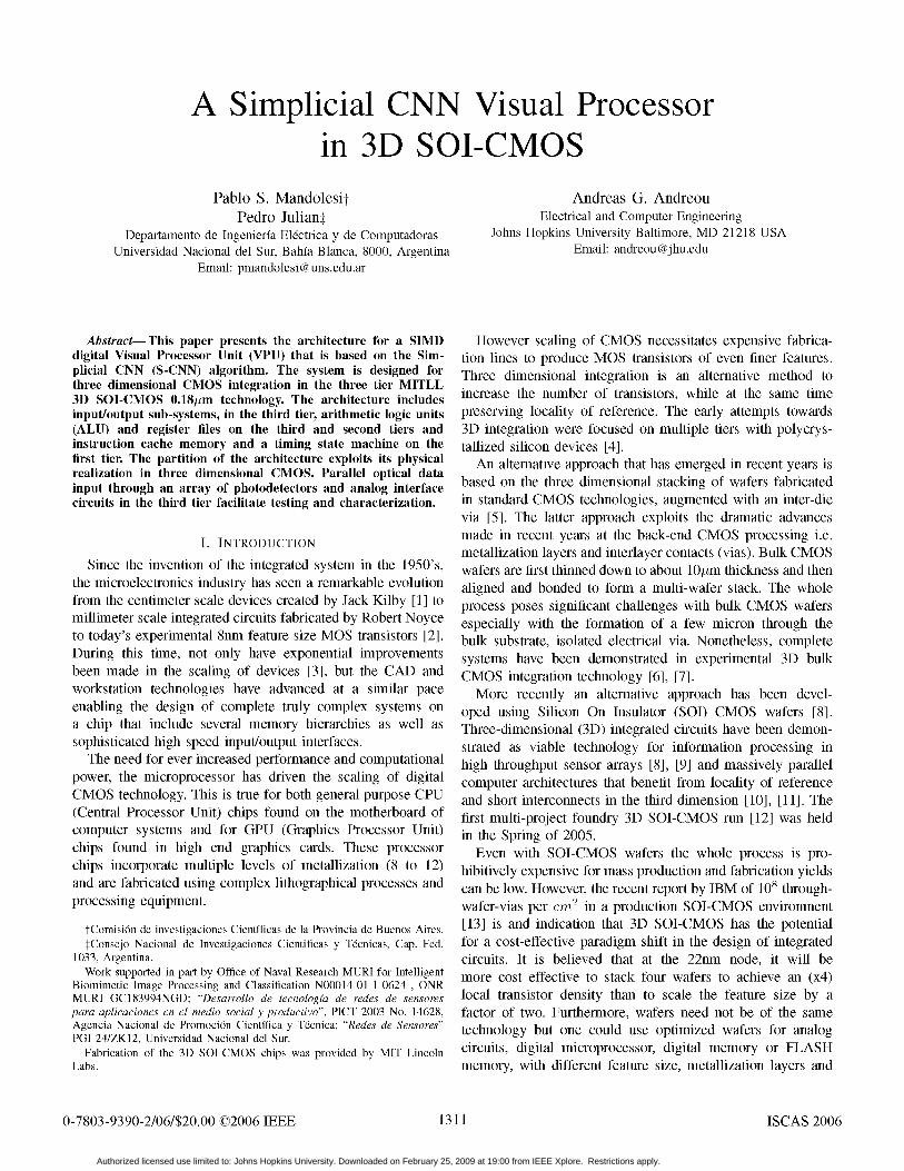
processor architecture and floor planning at the high level, a) b) c)Section III discusses the circuits in each cell of the arrayand the partition of the layout in the three tiers. Section IV Fig. 2. a) Tier 1 layout; b) Tier 2 layout; b) Tier 3 layoutconcludes the paper.
II. PROCESSOR ARCHITECTURE AND FLOOR PLAN machine, the instruction cache memory and part of the I/OIn this section we briefly summarize the salient features for subsystems on the sides of the array. Tier two and three
the architecture of the S-CNN processor presented in [17]. are occupied by arrays of ALU and register files as well asThe basic computation in the S-CNN SIMD architecture is input/output functions. Figure (2) shows the overall layouts ofdone sequentially in time on each cell over the entire array the individual tiers. On Tiers two and three the cell array canof cells in parallel. The processor functionality is determined be easily seen; two instruction cache memory banks and theby programming a set of memories describing the input and state machine on the side is evident in Tier 1. Each memorythe local cell state relationships, G and F respectively. This banks stores the information to run the programs and the blankis done for a group of cells called the sphere of influence space was left intentionally to add special test structures.(formed by a cell and its neighbors) and a simple logic relation In designing and partitioning the architecture in the threebetween them. Relation F : Ry-m > X and G : 'y-m X are tiers, care is taken to minimize the number of vias betweenpiecewise linear functions defined over a simplicial domain tiers (wafers). The vias in the targeted technology have dimen-(please see [17] [15]). During a program cycle, data encoded sions of 1.75 um and pitch of approximately 4 um. While thissequentially in time, and the evaluation of the composition is a remarkable achievement in an experimental technology,of functions F and G, namely FoG, evolve. The output of their size and spacing is not commensurate with the transistoreach cell is the integration of the binary value FoG during feature size in this technology (0.18,um). We have partition thethe complete program cycle. The input/state relationship of system architecture ensuring that only one through wafer viathe sphere of influence is determined by the mapping that is is used for each cell in the array of processing units. Linearstored in the G/F lookup table. Each lookup table consists of arrays of vias are however employed for data and control buses512 bits of memory. In the most general case of this processor on the sides of the array.architecture, each cell could have its own look up table. In 1. The cell array Block: The array is produced by tilingthe SIMD architecture describe here, all cells share the same identical cells in a regular grid. Each cell is 60,um by 60,umlookup table. The value of G/F is extracted by addressing the and two tiers tall. The circuits included on each cell handlememory with an ordered set of binary signals, the time coded data input, communicate to its neighbors the input and theinput/state values of the sphere of influence that form a nine-bit state of each cell, and interact with the periphery circuits todigital word. At completion of the program cycle, an eight- execute the selected program cycle, transfer results, or loadbit value is stored in the state register and can be transferred special inputs.outside the chip if desired. For a more detailed description of 2. The state machine and memory unit: The state machinethe underlying architecture and its programming the reader is includes all the circuits needed to synchronize the processorreferred to [17]. subsystems and in addition has the capacity to store the
The S-CNN processor consists basically of three main parts: programming functions. The state machine signals includethe cell array, the state machine/ memory units and the I/O the A/D conversion cycle for the Tier 3 diagnostic opticalinterface unit [see Figure (la)]. input, controls the I/O operations, the program cycle and the
Figure (ib) shows a sketch of the floorplan for the ar- function evaluation cycle control signals. The programs arechitecture mapped onto a three tier CMOS technology. Tier stored in four different memory banks, arranged in two doubleone is used for service circuitry including the processor state banks. Each bank has the state function look up table (F), the
1312
Authorized licensed use limited to: Johns Hopkins University. Downloaded on February 25, 2009 at 19:00 from IEEE Xplore. Restrictions apply.

Ronv, Col iBit
transducer U vs Rairp Neig bors UP s Vs G(. rn i ou U - 8IABts Comlparator, 1[J Pwm / Innuer Ramlp Latch lo,
a) Masks
In1put UPw..' n 7ARwp S J
register IBCLAt
Digit l Ilut its BU JS Digitl lRla7? If lner Ra ,) isBJ
2 Bits BtJS G(InnrR, )l
IBit
x
Fig. 3. a) Cell layout for Tier 3 b) Cell layout for Tier 2
input function look up table (G) and the composition logic the FoG operational block in Figure (3b). What is important,function (FoG). These circuits are located on Tier one and they is that this data is carried from one tier to the other throughcommunicate with the cell array and the I/O block through 3D a singe 3D via. The basic parts in each cell are:
visnnphepeiperaokteshi.1. The pixel or digital input: This circuit includes the3. The I/O interface: The I/O Interface contains the circuitsphotosensitiveelementandtheassociatedA/Dco
needed for each tier to interact with the external to the chip facilitate testability.and.diagnostics. In thendiagnosticseor "im-components2[seeFig.(1)]. The Bi/Ocnir allowsrth readoutcofpthendta, thee loaing of)] dTa, thepirogiraminalofstheleaook ager" mode, a single PIN photodiode (designed as an externalof hedaa, hel odtateofthlok ring in tier three, [see Figure (4)] integrates photocurrentup table and the configuration of the state machine. These int cpacitan tocgiv volae o u. The isfunctionFoGThscircuitsare located ontpy Thercp andsread isampled, held and compared to an external analog ramp thatout over the three tiers. The chip bonding pads are on the rn ycrnzdwt iia ap hnterm otgbackofmatier wthr top of the chi is greater than the photodiode voltage, the comparator changes
III. CELL DESCRIPTION AND FLOOR PLAN its output and the value of the digital ramp is latched. ThisThe cell structure is depicted in Figure (3) where the is a single slope parallel A/D converter and the input digital
blockddiarams(a)h andr (bintercres toeexternaltohreea value is stored in a register (the capability of loading an image
blockponents[seFg(a) The(b) corrcuindtry allow thre randou agrtweo inl I htdid dsge anetra
respectively. The 8 bit bus, the synchronization lines and the directly to the input register cell by cell also exists). These2ircbitbs lines showaten ineFerigure()re ommonetp eachrel circuits are all located on tier three the top of the wafer stackarray row. the output bus iS share bny a cell array column. allowing dir oniofdthea rray.The neighbor arrows depict the lines coming from all cells in 2. The encoder block: includes the circuits required forcell's sphere of influence; similarly, the pulse width modulated the time encoding of the input and state values (UPwm anddigital 1 bit data line (PWM) goes to all the cells in the XPwm). Every signal is coded with one bit in such a way thatneighborhood. The superimposed arrows show the information it is zero when the input (or state, respectively) is greater thantransmitted through the 8-bit bus at different processing stages. the cycle ramp and one otherwise. The encoders are two digitalOn the right of picture in Figure (3a) the one bit line with the comparators, one in Tier 3 [Fig. (3a)] for the input and one intime coded information of G connects to the right arrow on Tier 2 [Fig. (3b)] for the state. They compare the value of the
1313
Authorized licensed use limited to: Johns Hopkins University. Downloaded on February 25, 2009 at 19:00 from IEEE Xplore. Restrictions apply.

technology with similar feature size. The chip currently inm- fabrication includes a 14x 14 cell array, in a 1.25mm x 1.25mm
area with extra test structures in the blank areas. The cellularprocessor architecture has a density of '-~30, 000 through-wafer-vias per cm2, a rather small number compared to thedensities reported in [13], ensuring that the ultimate systemcould be manufactured with good production yields.
ACKNOWLEDGMENTSFig. 4. a) Cell tier three picture b) Cell tier two picture We thank Dr. Craig Keast for his personal interest and
support. This work was done while one of the authors (AGA)was on a sabbatical leave of absence at the Universidad
digital ramp with the stored digital values. As a result, two Nacional del Sur, Bahfa Blanca.control signals are obtained that are shared with all neighbors REFERENCESin the sphere of influence (UPwm and XPwm). Every cell [1] J. S. Kilby, "Turning potential into realities: The invention ofcollects nine pairs of these encoded signals, one per neighbor. the integrated circuit," http:/nobelprize.org/physics/laureates/2000/kilby-The UPwm signals run on Tier 3 and the XPwm signals run lecture.pdf, Dallas, TX, December 2000.
[2] ITRS, "International technology roadmap for semiconductors,"on Tier 2. http://public.itrs.net, 2005.
3. The processing block: This aggregates the vectors that [3] G. E. Moore, "Progress in digital integrated electronics," 1975 Interna-correspond to the inputs and states of the cells in the sphere tional Electron Devices Meeting, vol. 21, pp. 11-13, 1975.of influence in two digital time varying words Wu and Wx for [4] R. Buchner, W. VanDerWel, K. Haberger, S. Seitz, J. Weber, and
P. Seegebrecht, "Process technology for 3D-CMOS devices," in IEEEthe neighbors UPwm and the neighbors XPwm, respectively. SOS/SOI Technology Conference, October 1989, pp. 72 - 73.At each step of the cycle the value of function F and G [5] M. Koyanagi, H. Kurino, K. W. Lee, K. Sakuma, N. Miyakawa, and
H. Hitano, "Future system-on-silicon LSI chips," in IEEE Micro, July-at the vertices indicated by Wi and Wu are obtained. This August 1998, pp. 18 - 22.is done by comparing the broadcast of the memory address [6] H. Kurino, K. Lee, T. Nakamura, K. Sakuma, K. Park, N. Miyakawa,with Wu (and Wx) and latching the value of F (and G) H. Shimazutsu, K. Kim, K. Inamura, and M. Koyangi, "Intelligent image
sensor chip with three dimensional structure," Electron Devices Meeting,when a match between the inner ramp and Wu (Wi) occurs. 1999. IEDM Technical Digest International, pp. 879-882, Dec. 1999.These tasks are done with two digital comparators (8 bits [7] M. Koyanagy, Y. Nakagawa, K. W. Lee, T. Nakamura, Y. Yamada,each) and two multiplexers that are controlled by bit number K. Park, and H. Kurino, "Neuromorphic vision chip fabricated using9ofWu and Wx to select the lower or higher memory
three-dimensional integration technology," in IEEE International Solid-9 of Wu and Wz to select the lower or hlgher memory State Circuits Conference, vol. 1, February 2001, pp. 270 - 271.value. Broadcasting simultaneously two values of the memory [8] J. Burns, L. Mcllrath, J. Hopwood, C. Keast, D. Vu, K. Warner, andreduces the number of cycles in the inner instruction loop P. Wyatt, "An SOI three-dimensional integrated circuit technology," in
IEEE International SOI Conference, October 2000, pp. 20 - 21.(ramp) but adds complexity to the cell. After the two functions [9] V. Suntharalingam, R. Berger, J. Burns, C. Chen, C. Keast, J. Knecht,are evaluated, the result of the programmed logical operation R. Lambert, K. Newcomb, D. O'Mara, C. Stevenson, B. Tyrrell,FoG gives the value of the ramp step S-CNN function. This K.Warner, B. Wheeler, D.Yost, and D.Young, "CMOS image sensor
fabricated in three-dimensional integrated circuit technology," in IEEEbit iS integrated on a counter (accumulator). All the previous International Solid-State Circuits Conference, vol. 1, February 2005, pp.circuits are distributed on Tiers 3 and 2. Tier three has all 356 - 357.those components related to u and UPwm, and Tier two has [10] K. W. Lee, T. Nakamura, T. Ono, Y Yamada, T. Mizukusa,
t cm esFcircuits H. Hashimoto, K. T. Park, H. Kurino, and M. Koyanagi, "Three-thecomonntsreate t nd Pw , pustheFo dimensional shared memory fabricated using wafer stacking technology,"
and the integration counter. It is important to point out that the in IEEE International Electron Devices Meeting, 2000, pp. 165 - 168.partition of the processing blocks as described, requires only [11] X. Lei, C. C. Liu, H. S. Kim, S. K. Kim, and S. Tiwari, "Three-oneTier 2 to Tier 3 via for each cell. The via communicates dimensional integration: technology, use, and issues for mixed-signalone applications," IEEE Transactions on Electron Devices, vol. 50, pp. 601
the time coded results obtained on Tier 3 to Tier 2 to complete - 609, March 2003.the computation [Fig. (3)]. This is a fundamental characteristic [12] Massachusetts Institute of Technology Lincoln Laboratory, "MITLL
of our architecture thatminimizesthenumberoftilow-power FDSOI CMOS process design guide," June 2005.Of our architecture that minimizes the number of tier to tier [13] A. Topol and twenty eight other authors, "Enabling SOI-Based Assemblyvias in every cell of the array. Technology for Three-Dimensional (3D) Integrated Circuits (ICs)," in
Proceedings IEDM, 2005, pp. 363-365.IV. CONCLUSIONS [14] P. Julian, R. Dogaru, and L. 0. Chua, "A piecewise-linear simplicial
The (S-CNN) algorithm is especially suited to a 3D CMOS Circuits Syst. I,for C gray-levelimage processing," IEEE Transvarchitecture. The encoding of data in time, allows transfer [15] R. Dogaru, P. Julian, and L. 0. Chua, "The simplicial neural cell andof information from tier to tier through a minimal number its mixed-signal circuit implementation: An efficient neural network
architecture for intelligent signal processing in portable multimediaof vias and making more efficient use of space in the 3D applications," IEEE Trans. Neural Net., vol. 13, pp. 995-1008, Julyfloor planning. At the same time, because of pipelining and 2002.On chip instruction cache, data and instruction multiplexing [16] L. 0. Chua and L. Yang, "Cellular neural networks: Theory," IEEE
Trans. Circuits Syst. I, vol. CAS-35, pp. 1257-1272, October 1988.On the chip does not reduce the computational throughput [17] P. 5. Mandolesi, P. Julian, and A. G. Andreou, "A scalable and program-in the array. The 3D vias are small but not small enough mable simplicial CNN digital pixel processor architecture," Transactionsif compared with metal to metal vias in production CMOS on Circuits and Systems Part I, vol. 51, no. 5, pp. 988-996, May 2004.
1314
Authorized licensed use limited to: Johns Hopkins University. Downloaded on February 25, 2009 at 19:00 from IEEE Xplore. Restrictions apply.