A SET and Noise Fault Tolerant Circuit Design Technique ...
11
Abstract— In the near future of high component density and low-power technologies, soft errors occurring not only in memory systems and latches but also in the combinational parts of logic circuits will seriously affect the reliable operation of integrated circuits. In this paper, we present a novel design style that reduces the impact of radiation-induced single event transients (SET) on logic circuits, and enhances the robustness in noisy environments. This technology’s independent design style achieves SET mitigation and noise immunity by strengthening the sensitive nodes using a technique similar to feedback. We propose two alternatives for this methodology in 7nm FinFET, and, to check the accuracy of our proposal, we compare them with previous techniques for hardening radiation at the transistor level against a Single Event Transient. Simulation results show that the proposed method has a higher soft error tolerance capability than existing methods as well as better noisy immunity. Keywords — single event transient, soft error, radiation hardening, noise immunity. 1. Introduction With the continuous trend of device scaling and an increase in complexity, reliability is becoming a key issue. Factors such as transient errors, device degradation, noise immunity, and device variability (induced by manufacturing and operating conditions) are becoming very important [1] and they threaten to worsen overall circuit behavior. Regarding transient event errors, the susceptibility to environmental radiation is significantly increasing its effects in ultra-deep submicron circuits even at sea level [2][4], emerging as a key reliability concern for advanced deeper technologies. In memory cells, latches or flip-flops, alpha particle and neutrons induce a single event upset (SEU) by flipping a bit, whereas in combinational logic a single event transient (SET) is induced, producing an additional current which becomes a voltage pulse that may propagate through the logic and generating a soft error if it is latched by a memory element. Due to the scaling limitations of the classical CMOS structure, new devices are being investigated. These have been developed because of worsening reliability related with the scaling limit of the classical CMOS structure. Multiple-gate architectures, FinFET, are found to be one of the most promising solutions to overcome scaling limits such as short channel effect and the excessive threshold voltage variation [3]. FinFETs multi-gate structure allows for superior electrostatic gate control and their compatibility with CMOS makes them a suitable replacement of planar bulk CMOS devices [2]. Currently, semiconductor manufacturers regularly announce the production of transistors with gate lengths of 20 nm [5][6]. Moreover, the digital circuit trend is towards a lower voltage supply, which implies lower noise margins and smaller amounts of charge representing each bit of information. This trend causes the circuits to be more sensitive to any disturbance such as noise, crosstalk, or ionizing particles, and they thus present an increased susceptibility to soft errors [4]. With this trend, the charge required to generate a SET at a node decreases while the operating frequency of the circuits increases. Due to both of these effects, combinational logic errors are predicted to exceed flip–flop upsets for advanced technologies [16], and to increase their susceptibility to noise. For technologies with supply voltages under 1 V, these potential variations may result in unexpected vulnerability. In order to obtain a reliable system in noisy environments and under the effects of SET, several techniques have been developed to harden a node, or a circuit path at several design levels [1]. Some attempts to reduce the initial SET pulse width are focused at the struck logic cell, modifying the layout, such as a guard ring technique, quenching effects, guard drain technique or sizing the source [10][12][11]. These techniques are intended to reduce the SET impact, but they have minimal impact on the reliability in environments with low noise margins, or crosstalk. A well-known technique for hardening logic is based on transistor up-sizing [9]. If the value of the capacitance is increased, the charge required to generate a SET pulse also increases, thereby hardening the circuit node. This approach worked for older technologies where the node stored charge was significantly higher than a few femto Coulombs (fC). If the initial value of capacitance is only a few fF, as is the case for advanced technologies, the increase in capacitance values required to attenuate the transient becomes prohibitively high [14][15]. In [13] it is concluded that small devices collect less of the charge deposited by a radiation particle, in comparison to larger devices, and for small devices with medium or high-energy radiation particle strikes, the A SET and Noise Fault Tolerant Circuit Design Technique: Application to 7nm FinFET A. Calomarde, E. Amat, F. Moll, J. Vigara, A. Rubio Electronic Engineering Department, Universitat Politècnica de Catalunya
Transcript of A SET and Noise Fault Tolerant Circuit Design Technique ...
Abstract— In the near future of high component density and low-power technologies, soft errors occurring not only in memory systems
and latches but also in the combinational parts of logic circuits will seriously affect the reliable operation of integrated circuits. In this paper, we present a novel design style that reduces the impact of radiation-induced single event transients (SET) on logic circuits, and enhances the robustness in noisy environments. This technology’s independent design style achieves SET mitigation and noise immunity by strengthening the sensitive nodes using a technique similar to feedback. We propose two alternatives for this methodology in 7nm FinFET, and, to check the accuracy of our proposal, we compare them with previous techniques for hardening radiation at the transistor level against a Single Event Transient. Simulation results show that the proposed method has a higher soft error tolerance capability than existing methods as well as better noisy immunity.
Keywords — single event transient, soft error, radiation hardening, noise immunity.
1. Introduction With the continuous trend of device scaling and an increase in complexity, reliability is becoming a key issue. Factors such as
transient errors, device degradation, noise immunity, and device variability (induced by manufacturing and operating conditions) are becoming very important [1] and they threaten to worsen overall circuit behavior. Regarding transient event errors, the susceptibility to environmental radiation is significantly increasing its effects in ultra-deep submicron circuits even at sea level [2][4], emerging as a key reliability concern for advanced deeper technologies. In memory cells, latches or flip-flops, alpha particle and neutrons induce a single event upset (SEU) by flipping a bit, whereas in combinational logic a single event transient (SET) is induced, producing an additional current which becomes a voltage pulse that may propagate through the logic and generating a soft error if it is latched by a memory element.
Due to the scaling limitations of the classical CMOS structure, new devices are being investigated. These have been developed because of worsening reliability related with the scaling limit of the classical CMOS structure. Multiple-gate architectures, FinFET, are found to be one of the most promising solutions to overcome scaling limits such as short channel effect and the excessive threshold voltage variation [3]. FinFETs multi-gate structure allows for superior electrostatic gate control and their compatibility with CMOS makes them a suitable replacement of planar bulk CMOS devices [2]. Currently, semiconductor manufacturers regularly announce the production of transistors with gate lengths of 20 nm [5][6].
Moreover, the digital circuit trend is towards a lower voltage supply, which implies lower noise margins and smaller amounts of charge representing each bit of information. This trend causes the circuits to be more sensitive to any disturbance such as noise, crosstalk, or ionizing particles, and they thus present an increased susceptibility to soft errors [4]. With this trend, the charge required to generate a SET at a node decreases while the operating frequency of the circuits increases. Due to both of these effects, combinational logic errors are predicted to exceed flip–flop upsets for advanced technologies [16], and to increase their susceptibility to noise. For technologies with supply voltages under 1 V, these potential variations may result in unexpected vulnerability.
In order to obtain a reliable system in noisy environments and under the effects of SET, several techniques have been developed to harden a node, or a circuit path at several design levels [1]. Some attempts to reduce the initial SET pulse width are focused at the struck logic cell, modifying the layout, such as a guard ring technique, quenching effects, guard drain technique or sizing the source [10][12][11]. These techniques are intended to reduce the SET impact, but they have minimal impact on the reliability in environments with low noise margins, or crosstalk.
A well-known technique for hardening logic is based on transistor up-sizing [9]. If the value of the capacitance is increased, the charge required to generate a SET pulse also increases, thereby hardening the circuit node. This approach worked for older technologies where the node stored charge was significantly higher than a few femto Coulombs (fC). If the initial value of capacitance is only a few fF, as is the case for advanced technologies, the increase in capacitance values required to attenuate the transient becomes prohibitively high [14][15]. In [13] it is concluded that small devices collect less of the charge deposited by a radiation particle, in comparison to larger devices, and for small devices with medium or high-energy radiation particle strikes, the
A SET and Noise Fault Tolerant Circuit Design Technique: Application to 7nm FinFET
A. Calomarde, E. Amat, F. Moll, J. Vigara, A. Rubio Electronic Engineering Department, Universitat Politècnica de Catalunya
pulse width of the voltage glitch increases with load capacitance of the gate. For high-energy particles the technique can increase the transient pulse amplitude and duration making SET effect even worse [18].
At logic the level a good solution is the use of a logic mask [19][20], with the objective of hardening only the most sensitive nodes, but this technique requires a method to harden these selected nodes. At the transistor level, cross-coupled inverters as weak-latch before each memory element are proposed [22]. Also proposed is a low pass filter using a C-element [24], but it uses a flip-flop, and this introduces new vulnerability situations. Other approaches take advantage of the hysteresis property in a Schmitt Trigger to mask transient errors at its internal nodes [25]. Furthermore, transistor folding is used to divide the strike node into many other nodes [14], according to the number of parallel transistor segments used in the folding. However, the sensitive area is proportionally increased, especially in complex gates, due to the large increase of direct connection of the drain transistor to the gate output. Another solution, Rad-hard, another possible solution, attempts to change the source voltage of the transistor in order to obtain less sensitivity to a SET [32]. Neither addresses the problem of noise immunity. It is worth noting that due to supply voltage reduction, noise margin decreases, which in turn also reduces immunity.
In order to solve the problem of reliability against noise, several solutions have been published recently [27] [28], but none of them address the SET issue. One of the proposals designed to solve the problem of noise tolerance is based on the theory of Markov Random Field (MRF) [26] . Moreover, the Turtle concept [27] uses redundancy in the inputs, and the common feature for both differential solutions is the high noise immunity, but this requires a large number of transistors and has a proportional increase in susceptible nodes to SET.
In order to reduce the number of transistors, solutions with single inputs-outputs (not differential) are required, as recently used in Schmitt Trigger’s [28] as proposal. Schmitt increases the noise margin, by modifying the switch level depending on the output level, i.e. when the output is low, the transition to a high level is greater than when the output level is high. Although the noise margin increases, due to low supply voltages, this increase is small and it is not significant enough to substantially improve noise immunity and also causes an adverse effect when a disturbance (e. g. noise, single event) causes a flip in the output, and recovery to the correct output level occurs later because it has changed the output switch level.
This paper presents a novel technique based on strengthening the sensitive nodes using a technique similar to feedback to reduce the impact of SET and the effects of low noise margins in new technologies. Section II presents a new method to reduce susceptibility to SET and noise. In Section III, the proposed technique is compared with the transistor level hardening solutions previously outlined, and in Section IV outlines the conclusions of this work are exposed.
2. SET hardening at transistor level A static logic gate is composed of two networks: i) a pull-up network responsible for setting the high logic value to the output,
and ii) a pull-down network, responsible for transmitting the logic low to the output. If either network receive an impact or noise, and the effect reaches the gate output node, an incorrect value can be propagated up to a memory element.
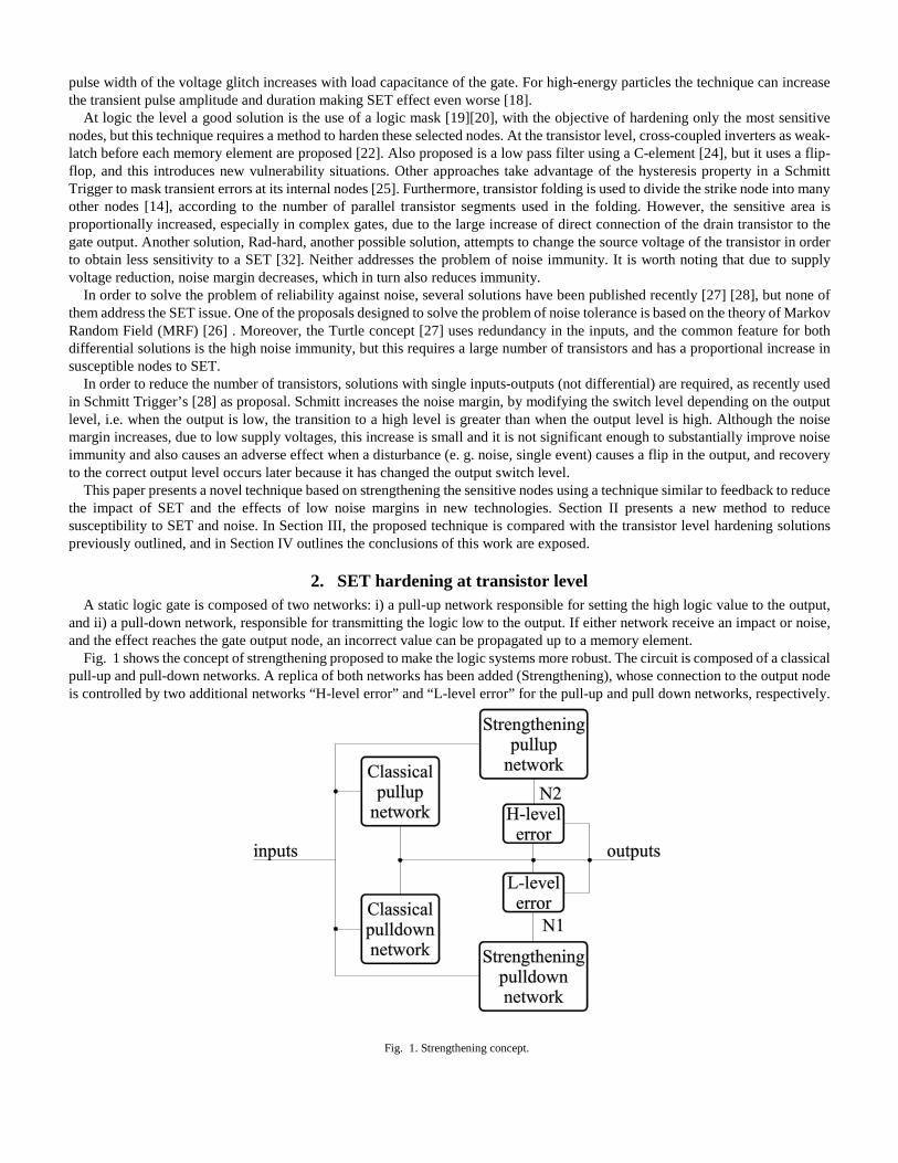
Fig. 1 shows the concept of strengthening proposed to make the logic systems more robust. The circuit is composed of a classical pull-up and pull-down networks. A replica of both networks has been added (Strengthening), whose connection to the output node is controlled by two additional networks “H-level error” and “L-level error” for the pull-up and pull down networks, respectively.
Fig. 1. Strengthening concept.
The function of the “H-level error” block is to monitor the output when a high level should be present at the output. So, if for whatever reason the gate output goes low (i.e. due to a SET or noise), the H-level error block connects the Strengthening pull-up to the stroked node, such that this network will attempt to recover the correct value by extracting the charge injected. On the other hand, the operation of the network “L-level error” is similar, but in this case the low output value is monitored and corrected if necessary. In the remaining situations, both H-level and L-level error networks, are always off (high impedance). In this context, strengthening networks will force the logical value whenever there is any kind of error (soft or single event). Note that this technique is technologically independent.
The reinforcement network, in the worst case, is a replica of the classical pull-up and pull-down, which will cover all possible situations, but usually, strengthening the output is not required for all input values but rather only for those who have no logical masking in the propagation path up to the next memory element or output [21]. Therefore, the area overhead is substantially reduced, For instance, in a NAND gate with “n” inputs, a low level output appears when “n” serial transistors are affected by a soft error. This situation has a low probability (1/2n) and may obviate in the “replicated pull-down network”, if the inputs have the same probability of both logic values.
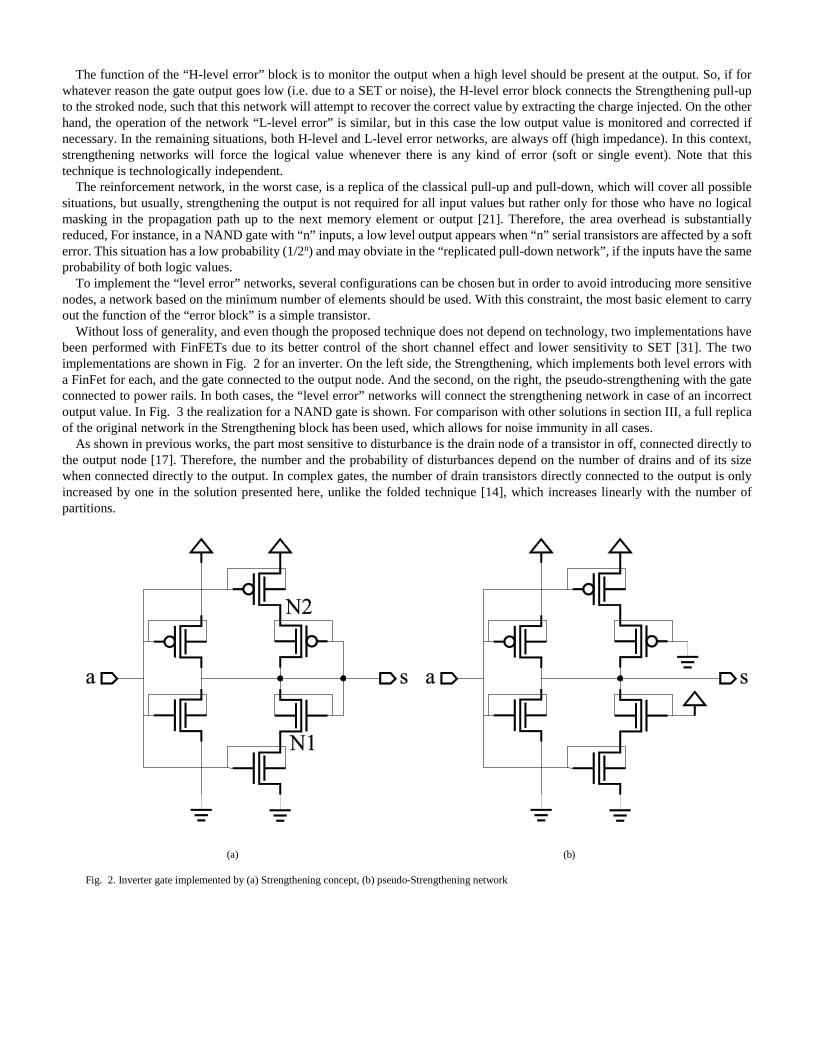
To implement the “level error” networks, several configurations can be chosen but in order to avoid introducing more sensitive nodes, a network based on the minimum number of elements should be used. With this constraint, the most basic element to carry out the function of the “error block” is a simple transistor.
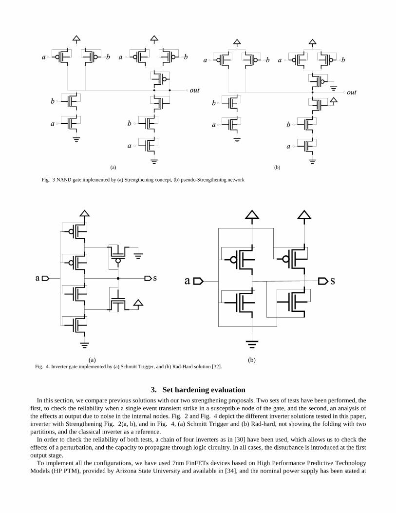
Without loss of generality, and even though the proposed technique does not depend on technology, two implementations have been performed with FinFETs due to its better control of the short channel effect and lower sensitivity to SET [31]. The two implementations are shown in Fig. 2 for an inverter. On the left side, the Strengthening, which implements both level errors with a FinFet for each, and the gate connected to the output node. And the second, on the right, the pseudo-strengthening with the gate connected to power rails. In both cases, the “level error” networks will connect the strengthening network in case of an incorrect output value. In Fig. 3 the realization for a NAND gate is shown. For comparison with other solutions in section III, a full replica of the original network in the Strengthening block has been used, which allows for noise immunity in all cases.
As shown in previous works, the part most sensitive to disturbance is the drain node of a transistor in off, connected directly to the output node [17]. Therefore, the number and the probability of disturbances depend on the number of drains and of its size when connected directly to the output. In complex gates, the number of drain transistors directly connected to the output is only increased by one in the solution presented here, unlike the folded technique [14], which increases linearly with the number of partitions.
(a) (b)
Fig. 2. Inverter gate implemented by (a) Strengthening concept, (b) pseudo-Strengthening network
3. Set hardening evaluation In this section, we compare previous solutions with our two strengthening proposals. Two sets of tests have been performed, the
first, to check the reliability when a single event transient strike in a susceptible node of the gate, and the second, an analysis of the effects at output due to noise in the internal nodes. Fig. 2 and Fig. 4 depict the different inverter solutions tested in this paper, inverter with Strengthening Fig. 2(a, b), and in Fig. 4, (a) Schmitt Trigger and (b) Rad-hard, not showing the folding with two partitions, and the classical inverter as a reference.
In order to check the reliability of both tests, a chain of four inverters as in [30] have been used, which allows us to check the effects of a perturbation, and the capacity to propagate through logic circuitry. In all cases, the disturbance is introduced at the first output stage.
To implement all the configurations, we have used 7nm FinFETs devices based on High Performance Predictive Technology Models (HP PTM), provided by Arizona State University and available in [34], and the nominal power supply has been stated at
(a) (b)
Fig. 3 NAND gate implemented by (a) Strengthening concept, (b) pseudo-Strengthening network
(a) (b) Fig. 4. Inverter gate implemented by (a) Schmitt Trigger, and (b) Rad-Hard solution [32].
Vdd = 0.7 v. The number of fins chosen for all solutions was 4 and 3 for the PFin and NFin, respectively. These values provide optimization of the delay-power product for the classic solution using four inverters of the same size as the load [29]. With these dimensions, the Schmitt Trigger obtains a low-to-high transition of 0.45 V. and high-to-low transition of 0.25 V, which gives a good threshold for the nominal Vdd = 0.7 V. Although in the other implementations, a better power-delay can be obtained with different fin sizes, we have kept the same size in order to make an accurate comoparison between the proposals.
3.1. Single Event Transient Impact To model the current generated by the incident ion, a current source in the strike node (the first stage of the chain inverters) has
been introduced. This strike is characterized by two collection phases: a first phase is characterized by a fast drift current, followed by a second phase of charge collection which produces a slow current diffusion due to the free carrier density gradients. The most sensitive region to an ion strike is the drain terminal in an off transistor due to E-field presence in the space charge region, so that it efficiently collects any charge generated in the vicinity.
A widely accepted shape for the current source is the double-exponential pulse [7][8]:
𝑖𝑖(𝑡𝑡) =𝑄𝑄
𝜏𝜏𝑓𝑓 − 𝜏𝜏𝑟𝑟�𝑒𝑒
−𝑡𝑡−𝑡𝑡0𝜏𝜏𝑓𝑓 − 𝑒𝑒−𝑡𝑡−𝑡𝑡0𝜏𝜏𝑟𝑟 �
Q represents the injected charge, and τf, τr are the fall and rise time constants of the current generated by the ion, that depend on particle impact location [33]. The critical charge (Qcrit) is known as the largest charge that can be injected into a sensitive node without changing its logical state. This magnitude mainly depends on both the width and amplitude of the current pulse [36]. In the literature, several values of injected charge and time constants have been reported in function to the approximation and the technology implemented [33]. These parameters have a direct relationship with the technology node, and to the best of our knowledge and beliefs, the nearest test made to the 7 nm FinFET was performed by [33][37] with 5nm. In these works the hit beam is generated with a backside laser with irradiation controlling its location from the fins underneath the drain. The results of the drain current exhibit several time constants, amplitudes of the current generated and the charge collected from 15 fC to 45 fC for a fin width of 5nm.
So, each SET has its unique characteristics, e.g. polarity, waveform, amplitude and duration, and these characteristics in turn depend on particle impact location, particle energy, device technology, supply voltage and output load. Therefore, to cover the location where the ion falls, and the energy required, a sweep of both parameters (the injected charge and the time constants) has been undertaken in order to ensure the effects in all possible situations. Subsequently the injected charge is swept from zero to a maximum of 45 fC as stated in [33] for 5 nm FinFETs, and the time constant from 1 ps to 30 ps, values that have been calculated by scaling the results from 20nm FinFET in [37]. The Fall Time Constant has been chosen as 2.2 times of the Rise Time [37].
The parameter measured, the “switching time (tth)” or “feedback time” [35] is defined as the time interval after the particle strikes during which the affected node voltage amplitude exceeds the gate threshold voltage (Vdd/2). This parameter states the time period that the logic gate presents a soft error due to a SET. This parameter can affect the reliability of the system, and force it to modify the clock period, i.e., a system with a refresh rate between memory elements (e.g. flip-flops, latches) of 20 Ghz, (50 ps period between samples), switching timing errors over this value will cause a soft error in nodes inside a logic sensitized path [21].
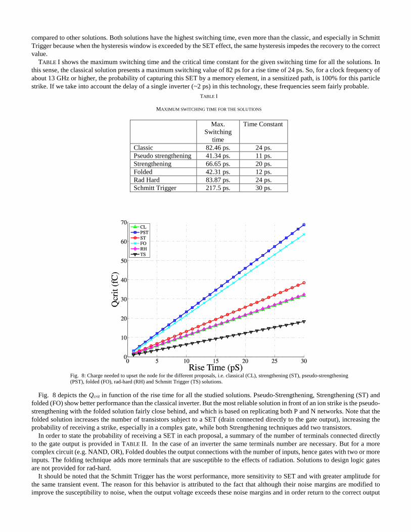
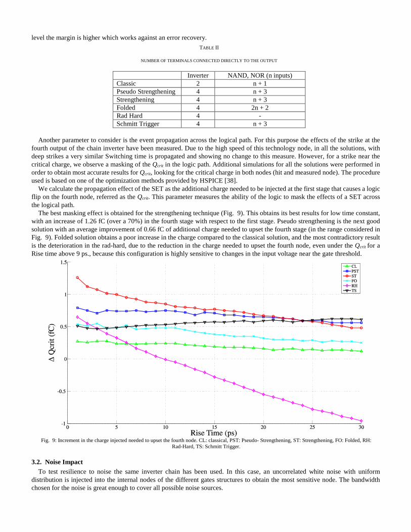
Figures 5, 6 and 7 depict the measured data at the first inverter output. The critical charge can be identified in the figures as the boundary between switching time zero and greater than zero and is summarized for all the proposals in Fig. 8. We observe that the critical charge depends on the time constant, because a higher constant needs higher injected charge to upset the node. It is also observed that for a given time constant, as the injected charge increases above the critical charge, the switching time increases as well, but some values achieve higher switching time.
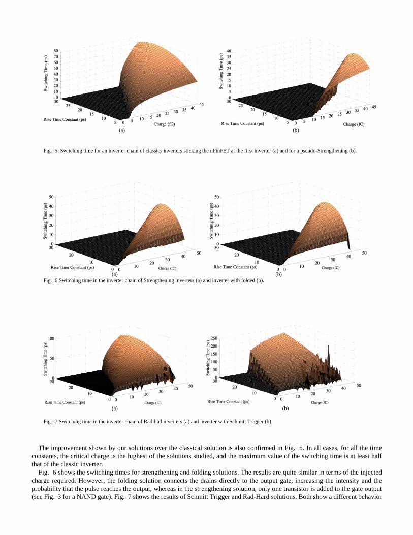
The improvement shown by our solutions over the classical solution is also confirmed in Fig. 5. In all cases, for all the time
constants, the critical charge is the highest of the solutions studied, and the maximum value of the switching time is at least half that of the classic inverter.
Fig. 6 shows the switching times for strengthening and folding solutions. The results are quite similar in terms of the injected charge required. However, the folding solution connects the drains directly to the output gate, increasing the intensity and the probability that the pulse reaches the output, whereas in the strengthening solution, only one transistor is added to the gate output (see Fig. 3 for a NAND gate). Fig. 7 shows the results of Schmitt Trigger and Rad-Hard solutions. Both show a different behavior
(a) (b)
Fig. 5. Switching time for an inverter chain of classics inverters sticking the nFinFET at the first inverter (a) and for a pseudo-Strengthening (b).
(a) (b)
Fig. 6 Switching time in the inverter chain of Strengthening inverters (a) and inverter with folded (b).
(a) (b)
Fig. 7 Switching time in the inverter chain of Rad-had inverters (a) and inverter with Schmitt Trigger (b).
compared to other solutions. Both solutions have the highest switching time, even more than the classic, and especially in Schmitt Trigger because when the hysteresis window is exceeded by the SET effect, the same hysteresis impedes the recovery to the correct value.
TABLE I shows the maximum switching time and the critical time constant for the given switching time for all the solutions. In this sense, the classical solution presents a maximum switching value of 82 ps for a rise time of 24 ps. So, for a clock frequency of about 13 GHz or higher, the probability of capturing this SET by a memory element, in a sensitized path, is 100% for this particle strike. If we take into account the delay of a single inverter (~2 ps) in this technology, these frequencies seem fairly probable.
Fig. 8 depicts the Qcrit in function of the rise time for all the studied solutions. Pseudo-Strengthening, Strengthening (ST) and
folded (FO) show better performance than the classical inverter. But the most reliable solution in front of an ion strike is the pseudo-strengthening with the folded solution fairly close behind, and which is based on replicating both P and N networks. Note that the folded solution increases the number of transistors subject to a SET (drain connected directly to the gate output), increasing the probability of receiving a strike, especially in a complex gate, while both Strengthening techniques add two transistors.
In order to state the probability of receiving a SET in each proposal, a summary of the number of terminals connected directly to the gate output is provided in TABLE II. In the case of an inverter the same terminals number are necessary. But for a more complex circuit (e.g. NAND, OR), Folded doubles the output connections with the number of inputs, hence gates with two or more inputs. The folding technique adds more terminals that are susceptible to the effects of radiation. Solutions to design logic gates are not provided for rad-hard.
It should be noted that the Schmitt Trigger has the worst performance, more sensitivity to SET and with greater amplitude for the same transient event. The reason for this behavior is attributed to the fact that although their noise margins are modified to improve the susceptibility to noise, when the output voltage exceeds these noise margins and in order return to the correct output
TABLE I
MAXIMUM SWITCHING TIME FOR THE SOLUTIONS
Max. Switching
time
Time Constant
Classic 82.46 ps. 24 ps. Pseudo strengthening 41.34 ps. 11 ps. Strengthening 66.65 ps. 20 ps. Folded 42.31 ps. 12 ps. Rad Hard 83.87 ps. 24 ps. Schmitt Trigger 217.5 ps. 30 ps.
Fig. 8: Charge needed to upset the node for the different proposals, i.e. classical (CL), strengthening (ST), pseudo-strengthening (PST), folded (FO), rad-hard (RH) and Schmitt Trigger (TS) solutions.
level the margin is higher which works against an error recovery.
Another parameter to consider is the event propagation across the logical path. For this purpose the effects of the strike at the
fourth output of the chain inverter have been measured. Due to the high speed of this technology node, in all the solutions, with deep strikes a very similar Switching time is propagated and showing no change to this measure. However, for a strike near the critical charge, we observe a masking of the Qcrit in the logic path. Additional simulations for all the solutions were performed in order to obtain most accurate results for Qcrit, looking for the critical charge in both nodes (hit and measured node). The procedure used is based on one of the optimization methods provided by HSPICE [38].
We calculate the propagation effect of the SET as the additional charge needed to be injected at the first stage that causes a logic flip on the fourth node, referred as the Qcrit. This parameter measures the ability of the logic to mask the effects of a SET across the logical path.
The best masking effect is obtained for the strengthening technique (Fig. 9). This obtains its best results for low time constant, with an increase of 1.26 fC (over a 70%) in the fourth stage with respect to the first stage. Pseudo strengthening is the next good solution with an average improvement of 0.66 fC of additional charge needed to upset the fourth stage (in the range considered in Fig. 9). Folded solution obtains a poor increase in the charge compared to the classical solution, and the most contradictory result is the deterioration in the rad-hard, due to the reduction in the charge needed to upset the fourth node, even under the Qcrit for a Rise time above 9 ps., because this configuration is highly sensitive to changes in the input voltage near the gate threshold.
3.2. Noise Impact
To test resilience to noise the same inverter chain has been used. In this case, an uncorrelated white noise with uniform distribution is injected into the internal nodes of the different gates structures to obtain the most sensitive node. The bandwidth chosen for the noise is great enough to cover all possible noise sources.
TABLE II
NUMBER OF TERMINALS CONNECTED DIRECTLY TO THE OUTPUT
Inverter NAND, NOR (n inputs) Classic 2 n + 1 Pseudo Strengthening 4 n + 3 Strengthening 4 n + 3 Folded 4 2n + 2 Rad Hard 4 - Schmitt Trigger 4 n + 3
Fig. 9: Increment in the charge injected needed to upset the fourth node. CL: classical, PST: Pseudo- Strengthening, ST: Strengthening, FO: Folded, RH:
Rad-Hard, TS: Schmitt Trigger.
The simulation time for all the cases was 10 ns, and measured the sum of all the failed intervals in the considered period, assuming a fault as the voltage that crosses the Vdd/2 value.
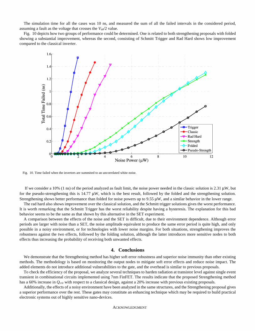
Fig. 10 depicts how two groups of performance could be determined. One is related to both strengthening proposals with folded showing a substantial improvement, whereas the second, consisting of Schmitt Trigger and Rad Hard shows low improvement compared to the classical inverter.
If we consider a 10% (1 ns) of the period analyzed as fault limit, the noise power needed in the classic solution is 2.31 µW, but
for the pseudo-strengthening this is 14.77 µW, which is the best result, followed by the folded and the strengthening solution. Strengthening shows better performance than folded for noise powers up to 9.55 µW, and a similar behavior in the lower range.
The rad hard also shows improvement over the classical solution, and the Schmitt trigger solutions gives the worst performance. It is worth remarking that the Schmitt Trigger has the worst reliability despite having a hysteresis. The explanation for this bad behavior seems to be the same as that shown by this alternative in the SET experiment.
A comparison between the effects of the noise and the SET is difficult, due to their environment dependence. Although error periods are larger with noise than a SET, the noise amplitude equivalent to produce the same error period is quite high, and only possible in a noisy environment, or for technologies with lower noise margins. For both situations, strengthening improves the robustness against the two effects, followed by the folding solution, although the latter introduces more sensitive nodes to both effects thus increasing the probability of receiving both unwanted effects.
4. Conclusions We demonstrate that the Strengthening method has higher soft error robustness and superior noise immunity than other existing
methods. The methodology is based on monitoring the output nodes to mitigate soft error effects and reduce noise impact. The added elements do not introduce additional vulnerabilities to the gate, and the overhead is similar to previous proposals.
To check the efficiency of the proposal, we analyze several techniques to harden radiation at transistor level against single event transient in combinational circuits implemented using 7nm FinFET. The results indicate that the proposed Strengthening method has a 60% increase in Qcrit with respect to a classical design, against a 20% increase with previous existing proposals.
Additionally, the effects of a noisy environment have been analyzed in the same structures, and the Strengthening proposal gives a superior performance over the rest. These gates may constitute an enhancing technique which may be required to build practical electronic systems out of highly sensitive nano-devices.
ACKNOWLEDGMENT
Fig. 10. Time failed when the inverters are summited to an uncorrelated white noise.
This research work has been undertaken with the support of the Spanish MINECO (JCI-2010-07083 and TEC2008-01856 with FEDER funds).
References [1] Mitra, S.; Brelsford, K.; Young Moon Kim; Hsiao-Heng Kelin Lee; Yanjing Li, “Robust System Design to Overcome CMOS Reliability Challenges”,
Emerging and Selected Topics in Circuits and Systems, IEEE Journal on , vol.1, no.1, pp.30-41, March 2011. [2] Technology Roadmap for Semiconductor (ITRS), online available: http://www.itrs.net/Links/2011ITRS/2011Chapters/2011PIDS.pdf [3] R. S. Muller, T. I. Kamins, and M. Chan, “Device Electronics for Integrated Circuits”, John Wiley and sons, 2003. [4] P. E. Dodd, M. R. Shaneyfelt, J. R. Schwank, and J. A. Felix, “Current and future challenges in radiation effects on CMOS electronics”, IEEE Tran. Nucl.
Sci., vol. 57, no. 4, pp. 1747–1763, Aug. 2010. [5] [Online]. http://www.eetimes.com/electronicsnews/4213622/TSMC-to make-FinFETs-in 450-mm-fab [6] [Online]. Available: http://www.eetimes.com/electronics-news/4215729/Intel-to-use-tri-gatetransistors-at-22-nm [7] Messenger, G.C., “Collection of Charge on Junction Nodes from Ion Tracks”, Nuclear Science, IEEE Transactions on, vol.29, no.6, pp.2024, 2031, Dec.
1982. [8] Gilson I. Wirth, Michele G. Vieira, Egas H. Neto, Fernanda Lima Kastensmidt, “Modeling the sensitivity of CMOS circuits to radiation induced single event
transients”, Microelectronics Reliability, Volume 48, Issue 1, January 2008, Pages 29-36. [9] Quming Zhou; Mohanram, K., “Gate sizing to radiation harden combinational logic”, Computer-Aided Design of Integrated Circuits and Systems, IEEE
Transactions on , vol.25, no.1, pp. 155- 166, Jan. 2006. [10] Amusan, O.A.; Massengill, L.W.; Bhuva, B.L.; DasGupta, S.; Witulski, A.F.; Ahlbin, J.R., “Design Techniques to Reduce SET Pulse Widths in Deep-
Submicron Combinational Logic”, Nuclear Science, IEEE Transactions on , vol.54, no.6, pp.2060-2064, Dec. 2007 [11] Jianjun Chen, Shuming Chen, Bin Liang, Biwei Liu, Fanyu Liu, “Radiation hardened by design techniques to reduce single event transient pulse width based
on the physical mechanism”, Microelectronics Reliability, Volume 52, Issue 6, June 2012, Pages 1227-1232. [12] Chen, J.; Chen, S.; He, Y.; Chi, Y.; Qin, J.; Liang, B.; Liu, B., “Novel Layout Technique for N-Hit Single-Event Transient Mitigation via Source-Extension”,
Nuclear Science, IEEE Transactions on , vol.59, no.6, pp.2859,2866, Dec. 2012. [13] Garg, R.; Khatri, S.P., “3D simulation and analysis of the radiation tolerance of voltage scaled digital circuit”, Computer Design, 2009. ICCD 2009. IEEE
International Conference on, pp.498-504, 4-7 Oct. 2009. [14] Kastensmidt, F.L.; Assis, T.; Ribeiro, I.; Wirth, G.; Brusamarello, L.; Reis, R., “Transistor sizing and folding techniques for radiation hardening”, Radiation
and Its Effects on Components and Systems (RADECS), 2009 European Conference on, pp.512-519, 14-18 Sept. 2009. [15] Mavis, D.G.; Eaton, P.H.; Sibley, M.D., “SEE characterization and mitigation in ultra-deep submicron technologies”, IC Design and Technology, 2009.
ICICDT ‘09. IEEE International Conference on, pp.105-112, 18-20 May 2009. [16] Mahatme NN et al., “Analysis of soft error rates in combinational and sequential logic and implications of hardening in advanced technologies”, Proceeding
of IEEE International Reliability Physics, Symposium; 2010. p. 1031–1035. [17] D. Munteanu and J.-L. Autran, “Modeling and Simulation of Single-Event Effects in Digital Devices and ICs”, IEEE Transactions on Nuclear Science, vol.
55, no. 4, pp. 1854–1878, 2008. [18] Assis, T.; Kastensmidt, F.L.; Wirth, G.; Reis, R., “Measuring the effectiveness of symmetric and asymmetric transistor sizing for Single Event Transient
mitigation in CMOS 90nm technologies”, Test Workshop, 2009. LATW ‘09. 10th Latin American, pp.1-6, 2-5 March 2009 [19] Nihaar N. Mahatme, Indranil Chatterjee, Akash Patki, Daniel B. Limbrick, Bharat L. Bhuva, Ronald D. Schrimpf, William Robinson, “An efficient technique
to select logic nodes for single event transient pulse-width reduction”, Microelectronics Reliability, Volume 53, Issue 1, January 2013, Pages 114-117. [20] S.N. Pagliarini, G.G. dos Santos, L.A. de B. Naviner, J.-F. Naviner, “Exploring the feasibility of selective hardening for combinational logic”,
Microelectronics Reliability, Volume 52, Issues 9–10, September–October 2012, Pages 1843-1847. [21] Sanchez-Clemente, A.; Entrena, L.; Garcia-Valderas, M.; Lopez-Ongil, C., “Logic masking for SET Mitigation Using Approximate Logic Circuits”, On-Line
Testing Symposium (IOLTS), 2012 IEEE 18th International, pp.176-181, 27-29 June 2012. [22] Haghi, M.; Draper, J., “Single-event transient mitigation in sub-micron combinational circuits”, Circuits and Systems (MWSCAS), 2011 IEEE 54th
International Midwest Symposium on, pp.1-4, 7-10 Aug. 2011. [23] J. Kumar and M.B. Tahoori, “Use of pass transistor logic to minimize the impact of soft errors in combinational circuits”, Workshop on System Effects of
Logic Soft Errors, 2005. [24] Uemura, T.; Tanabe, R.; Tosaka, Y.; Satoh, S., “Using Low Pass Filters in Mitigation Techniques against Single-Event Transients in 45nm Technology LSIs”,
On-Line Testing Symposium, 2008. IOLTS ‘08. 14th IEEE International, pp.117-122, 7-9 July 2008. [25] Sasaki, Y.; Namba, K.; Ito, H., “Soft Error Masking Circuit and Latch Using Schmitt Trigger Circuit”, Defect and Fault Tolerance in VLSI Systems, 2006.
DFT ‘06. 21st IEEE International Symposium on, pp.327-335, 4-6 Oct. 2006. [26] Nepal, K.; Bahar, R.I.; Mundy, J.; Patterson, W.R.; Zaslavsky, A., “Designing logic circuits for probabilistic computation in the presence of noise”, Design
Automation Conference, 2005. Proceedings. 42nd, pp. 485- 490, 13-17 June 2005. [27] Lancelot García-Leyva L.; Andrade D.; Gómez, S.; Calomarde, A.; Moll. F.; Rubio A., “New redundant logic design concept for high noise and low voltage
scenarios”, Microelectronics Journal, Volume 42, Issue 12, Pages 1359–1369, December 2011. [28] Takhirov, Z.; Nazer, B.; Joshi, A., “Error mitigation in digital logic using a feedback equalization with schmitt trigger (FEST) circuit”, Quality Electronic
Design (ISQED), 2012 13th International Symposium on, pp.312-319, 19-21 March 2012. [29] Weste N. H. E.; Harris, D. M.; “CMOS VLSI Design. A Circuits and Systems Perspective”, Ed. Addison-Wesley, 4th edition, 2011. [30] Munteanu, D.; Autran, J.-L., “Modeling and Simulation of Single-Event Effects in Digital Devices and ICs”, Nuclear Science, IEEE Transactions on, vol.55,
no.4, pp.1854-1878, Aug. 2008. [31] Eifert, N.; Gill, B.; Jahinuzzaman, S.; Basile, J.; Ambrose, V.; Quan Shi; Allmon, R.; Bramnik, A., “Soft Error Susceptibilities of 22 nm Tri-Gate Devices”,
Nuclear Science, IEEE Transactions on , vol.59, no.6, pp.2666,2673, Dec. 2012. [32] Rathod, S.S.; Saxena, A.K.; Dasgupta, S., “Rad-Hard 32 nm FinFET Based Inverters”, India Conference (INDICON), 2009 Annual IEEE, pp.1-4, 18-20 Dec.
2009. [33] El-Mamouni, F.; Zhang, E.X.; Pate, N.D.; Hooten, N.; Schrimpf, R.D.; Reed, R.A.; Galloway, K.F.; McMorrow, D.; Warner, J.; Simoen, E.; Claeys, C.;
Griffoni, A.; Linten, D.; Vizkelethy, G., “Laser- and Heavy Ion-Induced Charge Collection in Bulk FinFETs”, Nuclear Science, IEEE Transactions on, vol.58, no.6, pp.2563-2569, Dec. 2011.
[34] Predictive Technology Model website: http://ptm.asu.edu/ [35] Fan Wang; Agrawal, V.D., “Single Event Upset: An Embedded Tutorial”, VLSI Design, 2008. VLSID 2008. 21st International Conference on, pp.429, 434,
4-8 Jan. 2008. [36] Heijmen, T.; Giot, D.; Roche, P., “Factors that impact the critical charge of memory elements” On-Line Testing Symposium, 2006. IOLTS 2006. 12th IEEE
International T.
[37] El-Mamouni, F.; Zhang, E.X.; Ball, D.R.; Sierawski, B.; King, M.P.; Schrimpf, R.D.; Reed, R.A.; Alles, M.L.; Fleetwood, D.M.; Linten, D.; Simoen, E.; Vizkelethy, G., “Heavy-Ion-Induced Current Transients in Bulk and SOI FinFETs”, Nuclear Science, IEEE Transactions on , vol.59, no.6, pp.2674,2681, Dec. 2012.
[38] HSPICE reference manual. Synopsys.