
A PWM current-source inverter for interconnection · PDF fileA PWM current-source inverter for...
87
A PWM current-source inverter for interconnection between a photovoltaic array and the utility line Haan, de, S.W.H. Published: 01/01/1991 Document Version Publisher’s PDF, also known as Version of Record (includes final page, issue and volume numbers) Please check the document version of this publication: • A submitted manuscript is the author's version of the article upon submission and before peer-review. There can be important differences between the submitted version and the official published version of record. People interested in the research are advised to contact the author for the final version of the publication, or visit the DOI to the publisher's website. • The final author version and the galley proof are versions of the publication after peer review. • The final published version features the final layout of the paper including the volume, issue and page numbers. Link to publication Citation for published version (APA): Haan, de, S. W. H. (1991). A PWM current-source inverter for interconnection between a photovoltaic array and the utility line. (EUT report. E, Fac. of Electrical Engineering; Vol. 91-E-253). Eindhoven: Technische Universiteit Eindhoven. General rights Copyright and moral rights for the publications made accessible in the public portal are retained by the authors and/or other copyright owners and it is a condition of accessing publications that users recognise and abide by the legal requirements associated with these rights. • Users may download and print one copy of any publication from the public portal for the purpose of private study or research. • You may not further distribute the material or use it for any profit-making activity or commercial gain • You may freely distribute the URL identifying the publication in the public portal ? Take down policy If you believe that this document breaches copyright please contact us providing details, and we will remove access to the work immediately and investigate your claim. Download date: 24. Apr. 2018
Transcript of A PWM current-source inverter for interconnection · PDF fileA PWM current-source inverter for...
A PWM current-source inverter for interconnectionbetween a photovoltaic array and the utility lineHaan, de, S.W.H.
Published: 01/01/1991
Document VersionPublisher’s PDF, also known as Version of Record (includes final page, issue and volume numbers)
Please check the document version of this publication:
• A submitted manuscript is the author's version of the article upon submission and before peer-review. There can be important differencesbetween the submitted version and the official published version of record. People interested in the research are advised to contact theauthor for the final version of the publication, or visit the DOI to the publisher's website.• The final author version and the galley proof are versions of the publication after peer review.• The final published version features the final layout of the paper including the volume, issue and page numbers.
Link to publication
Citation for published version (APA):Haan, de, S. W. H. (1991). A PWM current-source inverter for interconnection between a photovoltaic array andthe utility line. (EUT report. E, Fac. of Electrical Engineering; Vol. 91-E-253). Eindhoven: Technische UniversiteitEindhoven.
General rightsCopyright and moral rights for the publications made accessible in the public portal are retained by the authors and/or other copyright ownersand it is a condition of accessing publications that users recognise and abide by the legal requirements associated with these rights.
• Users may download and print one copy of any publication from the public portal for the purpose of private study or research. • You may not further distribute the material or use it for any profit-making activity or commercial gain • You may freely distribute the URL identifying the publication in the public portal ?
Take down policyIf you believe that this document breaches copyright please contact us providing details, and we will remove access to the work immediatelyand investigate your claim.
Download date: 24. Apr. 2018

A PWM Current - Source I nverter for Interconnection between a Photovoltaic Array and the Utility Line
by S.w.H. de Haan
EUT Report 91 -E - 253 ISBN 90 - 6144 - 253 - 2
July 1991

ISSN 0167-9708
Eindhoven University of Technology Research Reports
EINDHOVEN UNIVERSITY OF TECHNOLOGY
Faculty of Electrical Engineering
Eindhoven, The Netherlands
A PWM CURRENT-SOURCE INVERTER FOR
INTERCONNECTION BETWEEN A PHOTOVOLTAIC
ARRAY AND THE UTILITY LINE
by
S.W.H. de Haan
EUT Report 91-E-253
ISBN 90-6144-253-2
Eindhoven
July 1991
Coden;TEUEDE
CIP-GEGEVENS KONINKLIJKE BIBLIOTHEEK, DEN HAAG
Haan, S.W.H. de
A PWM current-source inverter for interconnection between a photovoltaic
array and the utility line I by S.W.H. de Haan. - Eindhoven: Eindhoven
University of Technology, Faculty of Electrical Engineering. - Fig.,
tab. - (EUT report, ISSN 0167-9708; 91-E-253)
Met lit. opg., reg.
ISBN 90-6144-253-2
NUGI 832
Trefw.: invertor
ii

Abstract
A 3-phase transformer less power electronic conversion system is used as an
interface between a photovoltaic array and the utility line.
Because of the absense of a power transformer, and because of a high array
voltage, the efficiency is high. An MPPT is used for optimal utilisation of
the PV array, which results in a high yield of the system.
The power electronic converter is based on the topology of a Pulse Width
Modulated Current Source Inverter (PWM-CSI).
The inverter is operated at a high switching frequency (20 klHz) , so that
waveforms with a low distortion are generated, while the power factor is
near unity.
Two modulations are described, both based on sinusoidal modulation prelimi
nary test results are shown.
Address of the author:
Group Electromechanics and Power Electronics
Faculty of Electrical Engineering
Eindhoven University of Technology
P.O. Box 513
5600 MB EINDHOVEN
The Netherlands
iii
TABLE OF CONTENTS
1.
2.
3.
4.
5.
6.
7.
8.
9.
INTRODUCTION
DESCRIPTION OF THE POWER SYSTEM . . . . . . . . . . . . . . . . .
PRINCIPLE OF OPERATION
PULSE WIDTH MODULATION
4.1
4.2
CSI-modulation method # 1
CSI-modulation method # 2
DC-LINK
5.1 The DC-link current
5.2 Required value of Ld
5.3 High-frequency model of the
CONTROL ...
DC-link side of
6.1
6.2
Dynamic model of the conversion system
The TUE-maximum power point tracker (MPPT)
HARDWARE
7.1
7.2
7.3
7.4
7.5
Power-stage
Modulators
Watching electronics
Auxiliary boards
Checklist for powering up and down
the inverter
TEST RESULTS; OBSERVED WAVE FORM DISTORTION ......... .
8.1
8.2
8.3
Test results
Line induced DC-ripple
Harmonic currents and voltages in the AC-line
POWER CONSUMPTION AND EFFICIENCY
iv
1
4
6
10
10
15
16
16
21
22
24
24
26
27
27
27
30
30
31
33
33
36
38
42
10. CONCLUSIONS AND FINAL REMARKS . . . . . . . . . . . . . . . . .
11. REFERENCES
APPENDICES .............................
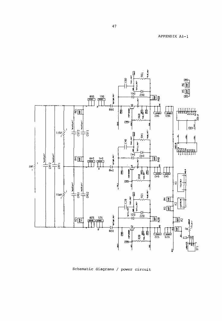
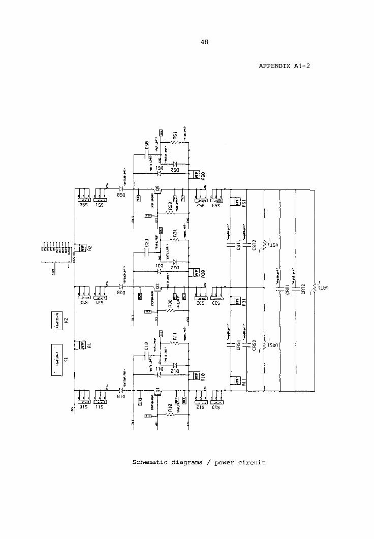
A. Schematic diagrams
1) power circuit and drivers
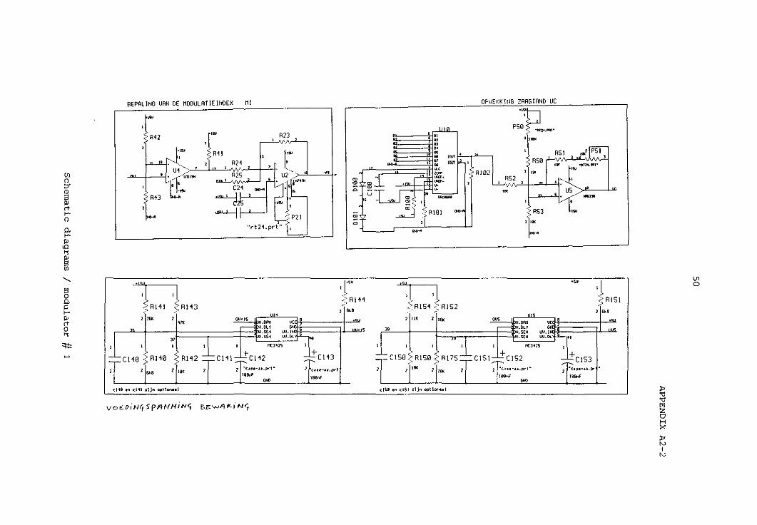
2) modulator # 1
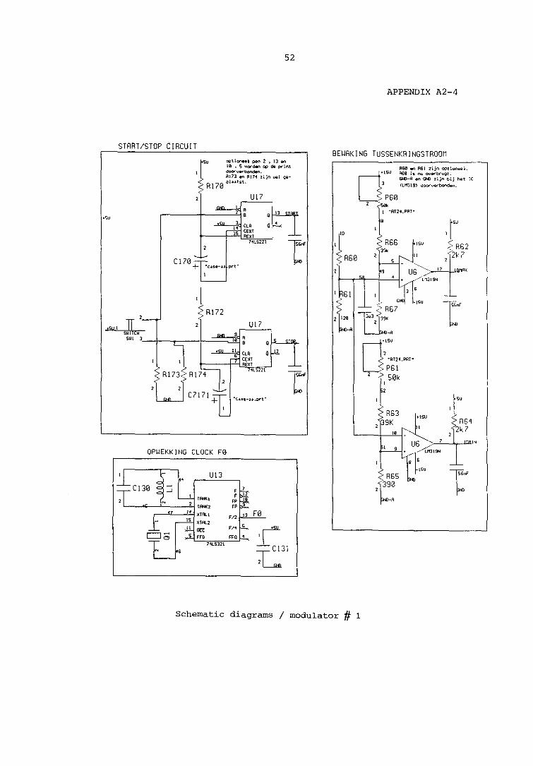
3) modulator # 2
4) TUE-MPPT
5) Isolation amplifiers
B. State machine diagrams
1)
2)
modulator
watching electronics
C. EPLD-definition
1)
2)
3)
4)
5)
6)
7)
EPLD-pinning
modulator # 1 + watching electronics
watching electronics (BEV02 - BEVOI + timer)
timer
BEVOI definition file
modulator definition file
MOD (generation of C.F signals)
D. Frequency spectra of the line-current at full load
1) Log spectrum 0 50 kHz
2) Log spectrum 0 6 kHz
3) Lin spectrum 0 6 kHz
4) Lin spectrum 0 50 kHz
v
44
46
47
47
49
54
56
58
60
61
62
63
64
65
66
68
72
73
74
75
76

vi

LIST OF SYMBOLS
id (t)
Id
ir,s,t(t)
i dpp
i dp
~
Ua(t)
ur,s,t(t)
Ud (t)
Ud
u
U
switching frequency
current in the solar array
ripple component in ia
DC-link current
averaged DC-link current
line currents
peak-to-peak value of the current-ripple component of id
ripple amplitude of the current-ripple component
DC-link inductance
voltage of the solar array
ripple component in Us
carrier
carrier amplitude
line-to-neutral voltages
DC-link voltage
averaged DC-link voltage
amplitude of the line-to-neutral voltages
rms value of the line-to-neutral voltages
vii
1
1. INTRODUCTION
Under contract of NOVEM the institute Netherlands Energy Research Foun
dation (ECN) has carried out a comparative analysis between two power
electronic conversion systems which serve the interconnection of a photo
voltaic array and the utility grid.
The comparison concerns the so called Fraunhofer inverter, which was
purchased by ECN from the Fraunhofer institute, and the PWM current-source
inverter (PWM-CSI), which has been developed by the Eindhoven University of
Technology (TUE) as a subcontractor of ECN.
The objective of this pilot project is to show that a PWM-CSI is suited for
photovoltaic energy conversion.
In this report this inverter is described.
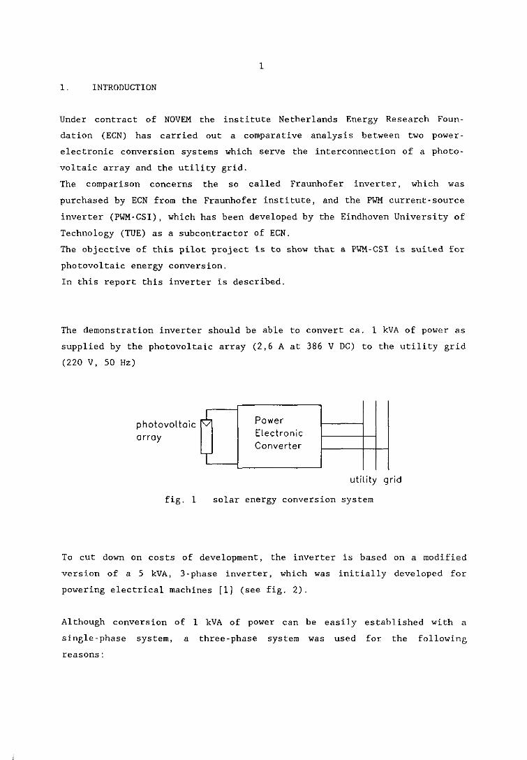
The demonstration inverter should be able to convert ca. 1 kVA of power as
supplied by the photovoltaic array (2,6 A at 386 V DC) to the utility grid
(220 V, 50 Hz)
photovoltoic array
fig. 1
~
L
Power Electronic Converter
utility grid
solar energy conversion system
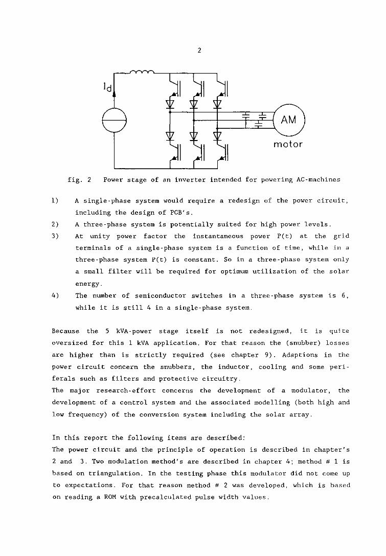
To cut down on costs of development, the inverter is based on a modified
version of a 5 kVA, 3-phase inverter. which was initially developed for
powering electrical machines [lJ (see fig. 2).
Although conversion of 1 kVA of power can be easily established with a
single-phase system, a three-phase system was used for the following
reasons:
2
motor
fig. 2 Power stage of an inverter intended for powering AC-machines
1) A single-phase system would require a redesign of the power circuit,
including the design of PCB's.
2) A three-phase system is potentially suited for high power levels.
3) At unity power factor the instantaneous power pet) at the grid
terminals of a single-phase system is a function of time, while in a
three-phase system pet) is constant. So in a three-phase system only
a small filter will be required for optimum utilization of the solar
energy.
4) The number of semiconductor switches in a three-phase system is 6,
while it is still 4 in a single-phase system.
Because the 5 kVA-power stage itself is not redesigned, it is quite
oversized for this 1 kVA application. For that reason the (snubber) losses
are higher than is strictly required (see chapter 9). Adaptions in the
power circuit concern the snubbers. the inductor. cooling and some peri
ferais such as filters and protective circuitry.
The major research-effort concerns the development of a modulator, the
development of a control system and the associated modelling (both high and
low frequency) of the conversion system including the solar array.
In this report the following items are described:
The power circuit and the principle of operation is described in chapter's
2 and 3. Two modulation method's are described in chapter 4; method # 1 is
based on triangulation. In the testing phase this modulator did not come up
to expectations. For that reason method # 2 was developed, which is based
on reading a ROM with precalculated pulse width values.

3
Because a significant current ripple in the solar array will reduce the
utilization of the array, the ripple-content of the waveforms is considered
extensively in chapter 5.
Based on the waveform analysis from chapter 5, an approximate model of the
conversion system is given which is both valid for frequences near the
switching frequency of the inverter as well as for low frequences (50 Hz).
The high frequency model is used to calculate the high-frequency ripple
reduction. In chapter 6 the control system is described. The low frequency
model mentioned above is used to design the control system.
The actual hardware, including blockdiagrams, is described in chapter 7.
Initially it as assumed that the harmonics in the utility grid could be
neglected. While testing it appeared that harmonic currents are present. In
chapter 8 the waveform distortion is considered.
Losses as occurring in semiconductors, snubbers, drivers, fans and control
electronics are considered in chapter 9.
In chapter 10 some test results are shown.
4
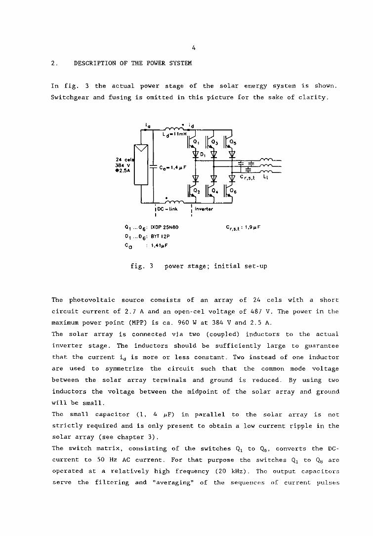
2. DESCRIPTION OF THE POWER SYSTEM
In fig. 3 the actual power stage of the solar energy system is shown.
Switchgear and fusing is omitted in this picture for the sake of clarity.
24 eel 384 V .2,5A
• , I DC -link 1
0 1 ... 0 6 , IXDP 2SN8D
°1 .. ·D 6 :BYTI2P
Co 1.41pF
C r,s,t Ll
I. I ,n"'ert.r
fig. 3 power stage; initial set-up
The photovoltaic source consists of an array of 24 eels with a short
circuit current of 2.7 A and an open-eel voltage of 487 V, The power in the
maximum power point (MPP) is ca. 960 W at 384 V and 2.5 A.
The solar array is connected via two (coupled) inductors to the actual
inverter stage. The inductors should be sufficiently large to guarantee
that the current id is more or less constant. Two instead of one inductor
are used to symmetrize the circuit such that the common mode voltage
between the solar array terminals and ground is reduced. By using two
inductors the voltage between the midpoint of the solar array and ground
will be small.
The small capacitor (1, 4 ~F) in parallel to the solar array is not
strictly required and is only present to obtain a low current ripple in the
solar array (see chapter 3).
The switch matrix, consisting of the switches Q1 to Q6. converts the De
current to 50 Hz AC current. For that purpose the switches Ql to Q6 are
operated at a relatively high frequency (20 kHz). The output capacitors
serve the filtering and "averaging ll of the sequences of current pulses

5
which are generated by the switch matrix. Inductances beLween the inverter
and the utility line are required to block the high- frequency current
components which are generated by the inverter.
Because unity power factor is persued, the instantaneous currents ir(t).
i,(t) and it(t) should be proportional to uro(t), u,o(t) and uto(t), where
the voltage reference node 0 is chosen, such that uro + Usc + u to = o.

6
3. PRINCIPLE OF OPERATION
Define so called switching cycles which are small time intervals of
duration Ts. which are linked up. The switching period Ts is supposed to be
much smaller than the period of the fundamental of the utility. The inverse
of Ts is called the switching frequency fs' which is 20 kHz in the con
verter considered. During each switching cycle a certain algorithm is
carried out, which renders control (- on/off) signals for the power
semiconductors. For those who are familiar with "carrier modulation" in
Voltage Source Inverters, it is mentioned that the switching cycle Ts cor
responds to the period of the triangular carrier.
During each switching cycle each of the lines r, sand t is supplied with a
current pulse of either positive or negative sign. For instance if Q1 and
Q4 are conducting. then line r will get positive current and line swill
get negative currrent. The height and duration of the current-pulse is
determined by the magnitude of the DC-link current and the on-time of the
related switch. Essentially the switch matrix serves the distribution of
chops of the DC-link current over the output lines.
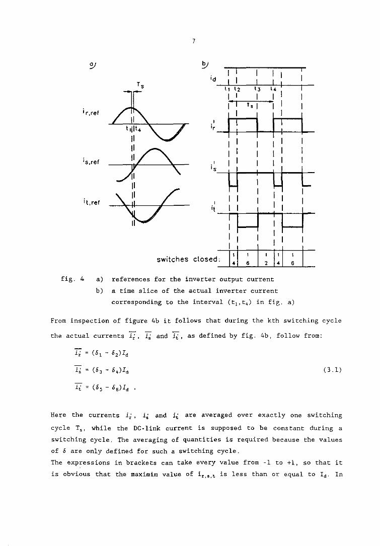
Suppose that the converter, including the capacitors, should generate
currents i r , is and it according to references ir ,ref' is, ref and it, ref
respectively. Consider a small time slice of a duration equal to the
switching period Ts (typically 50 ~s in our inverter) and beginning at time
t i . The instantaneous values of the desired output currrents iref,r to iref,t
at that time follow from figure 4a. Because the switching cycle Ts is
assumed to be very small with respect to the fundamental period of the
output waveforms, the references are considered constant during a switching
cycle.
Define the duty cycle om of switch Q., (mf (l .. 6)) by Om ~ Tm.on/Ts , where Ton
is the on-time of the switch considered and where Ts is the switching
period. The objective of the switching is to produce in each line and
during a part of each switching cycle Ts a current pulse whose average
value in a time slice Ts at time tl is equal to iref(t l ) for that line. This
complies with the idea that the output capacitors are only present to
average the pulsating currents which are generated by the current-fed
switching matrix.
7
V V id
I I I Ts I I I I
t I t2 t3 t.
I I I I I I I T s I I I
i r,ref
II I II II t llit. ir : :
II I I I I Ii/'\. I I I I is.ref II I I I
P I
:J' is
W II \.11 /' i t,ref I I
17 I
I I it I
I I I I I I I I
i: I I I: I switches closed: 6 2 6
fig. 4 a) references for the inverter output current
b) a time slice of the actual inverter current
corresponding to the interval (t"t,) in fig. a)
I
I I I I
L
From inspection of figure 4b it follows that during the kth switching cycle
the actual currents i~. i~ and it, as defined by fig. 4b, follow from:
l' s (3.1)
Here the currents i~. i~ and it are averaged over exactly one switching
cycle Ts. while the DC-link current is supposed to be constant during a
switching cycle. The averaging of quantities is required because the values
of 0 are only defined for such a switching cycle.
The expressions in brackets can take every value from -1 to +1, so that it
is obvious that the maximim value of ir,s,t is less than or equal to rd' In
8
general the value of ld will be chosen only slightly above the peak value
of the desired line current, in order to keep losses low.
The ratio between the peak value of the AC currents i ref and Id can be
associated with a modulation index Mi'
Because i~ + i~ + it = 0 , it follows from (3.1) that °1 + 03 + 55 = °2 + 54 + 0 6 ,
To prevent a) an open circuit for the inductor current and b) a short of
the output capacitors, it is required that both at the positive and at the
negative rail one and only one switch is conducting at a time. This means
that:
51 + 03 + 55 1
°2+ 0,+°6 1 (3.2)
In contrast to the VSI, shoot-through states are allowed, and even neces
sary to be able to generate sinusoidal currents and to be able to operate
in voltage step-up mode.
It has been shown [1) that for a sufficiently large switching frequency f"
with w,C l> 1 and woC <i! 1, the low frequency content of i~ is equal to the
low frequency content of i r .
Because the conditions above are fulfilled, the primes will be omitted for
50 Hz (- low frequency) signals.
To obtain sinusoidal line currents, the o's of the CSI should be modulated
such that they obey the following relations.
(01 ( 2 )' Hi sin (wot)
(03 0,)' Hi sin (wot 21f/3)
(05 ( 6 )' Hi sin (wot - 41f/3)
where Mi is called the modulation index (0 < Mi < 1).
From (3.1) and (3.3) it follows quite straightforward that:
ir = Hi Id sin wot
i, ' Hi Id sin (wot - 21f/3)
it ' Hi Id sin (wot - 41f/3)
(3.3)

9
Note that Mi gives the ratio between the DC-link current and the amplitude
of the line currents.
10
4. PULSE WIDTH MODULATION
Proper pulse patterns can be generated by a kind of carrier modulation,
which is a modified version of carrier modulation in VSI's.
In a carrier modulator for VSI's, a triangular carrier is compared with a
reference signal which reflects the desired output voltage of the respec
tive line. Depending on the outcome of the comparison either the upper or
the lower switch in the associated inverter leg is closed. This way of
modulation guarantees that a shoot through will not occur.
In a CSI it is required that we get control signals such that:
1°) (8, - 82 ) should be equal to ir.roriId etc.,
2°) exactly one switch is conducting at the upper rail,
3°) exactly one switch is conducting at the lower rail.
If we would use the VSI modulator described above and would replace the
references for output voltages by references for output currents, then
condition 1) will be satisfied, however constraints 2) and 3) may be
violated.
So we will need a modified modulator.
4.1 CSI-modulation method # 1
Because the inverter should operate at unity power factor, three references
for the output currents can be obtained from the output voltages according
to:
[ ~r.ref (t») ~s.ref (t)
it. ref (t)
(4.1)
where the reference node for the line voltages is chosen such that u ro + usa
+ u to = 0
Now define three signals u" u2 and u3 such that (see fig. 5)
k z lira = Uz - u, kz Usa = U3 - U2 (4.2) k z Uto = U1 - U3

11
where k z is an arbitrary scaling factor.
The following set of values of Ul. Uz and u3 (a non-unique set) satisfies
equation 4.2:
U, = k2 Uto - Uro
3
U2 = k2 Uro - usc (4.3)
3
U3 k2 Uso - Uto
3
In this way the differences between the signals u l • li2 and U3 correspond to
the desired output current i r •ref • is,ref and it,ref .
To get control signals which comply with the constraints mentioned above, a
saw-tooth carrier lie is generated and compared with lil' Uz and u3 (see fig.
5). From three comparator output signals it can be easily deduced which
swi tches should be turned on. For ins tance if lie > lil and lie > liZ then
switch 1 should be turned on, because Uz - Ul correspond to uro If uc(t) is
outside the envelope of ul, liZ and u3. then a shoot through state should be
generated.
To minimize the number of switching actions, the shoot through is realized
via the inverter leg which is connected to the phase that carries the
largest current in the time interval considered.
In fig. 6 the three signals Ul, Uz and u3 are shown. At any time the carrier
can take any value between + Uc and - uc .
It is shown which switch should be turned on if U c is in the region
indicated. If the carrier frequency is much higher than the frequency of
the utility line, then it follows from an examination of fig. 5b that the
duty cycles at time tl follow from
U2(t,) - u , (t,)
2uc

carrier u c
u
u, I
I I
" I I I I I I
! 1 5, I I I I I I
H II
" n I I II
5.----+I~i,-~i~I----I I I I I
·.-----+i+r-i-+~:~:~--I I I II
I I I I I
I I I 5.-----L1+1-T1~1~1~--
I I I I I I I I I
clock 20 kHZ~ I I ITs I I
12
I! I I I
shootthrough )' J l '~ShootthrOUgh bottom / ~ top
1 e pulse 2 e pulse
.. 3
fig, 5 Modulation principle
5 /
~ t
r
s

13
fig. 6 Switches to be closed
Ur = U2- U l
US=u3- u2
Ut=Ul-U3
U c : carrier
(4.4)
From eq. (4.4) and (3.1) it follows that the line currents will be propor
tional to the line voltages, provided Id is constant.
From fig. Sa it also follows that eq. (4.4) is valid only if li, exceeds the
peak value of Ul. U2 or U3'
Symmetrical grid
Assume a symmetrical grid according to:
(4. S)
From (3.4), (3.S) and (3.6) it follows that

14
(5, - 62 ) k2 u sin wot ~
(53 - 6,) k2 U sin (wot - 2" ) (4.6) ~ j
(5, - 6,) k2 u. sin ( 4" ~
Wo - j)
To be able to control the modulation index of the inverter the coefficient
k 2u/2uc should be equal to desired modulation index Mi. so:
(4.7)
The modulation depth can be controlled by controlling the scaling factor
k 2 ·
Linear control region
The output currents are only proportional to k2 if eq. (4.5) is valid.
As stated before eq. (4.4) is only valid if U, exceeds the peak value ua of
the auxiliary signals ul' Uz and u3 .
So the modulation operates in linear mode if:
(4.8)
From (4.3) and (4.5) it follows that
(4.9)
From (4.8) and (4.9) it follows for linear mode:
(4.10)

15
From (4.7) and (4.10) it is finally concluded that the modulator operates
in linear mode (i.e. output currents according to equal (4.1) only if
( 13_ Hi ""2 - 0.866
Because the system is designed to operate at Mi
way of modulation is appropriate.
Note:
(4.11) .
0.822 in the MPP, this
In connection with eq. (4.3) it has been stated that the set from eq. (4.3)
is not a unique solution of eq. (4.2). By adding an appropriate time
dependent term to eq. (4.2), the linear region can be extended to Mi ~ 1.
4.2 CSI-modulation method # 2
From experiments with modulator # 1, it was concluded that this modulator
did have some drawbacks; these are described in sections 8.2 and 8.3.
To be able to obtain an inverter which generates high quality wave form, it
was decided to use a different type of modulator which had proven to be
insensitive to noise and other environmental interactions.
The method is based on generation of a precalculated switching pattern for
the semiconductors. A ROM is used to store a set numbers which represents
on/off times of semiconductor switches. The on/off times are calculated
such that they are in accordance with eq. (3.3) at Hi = 1. The values which
are coming from the ROM are multiplied by Hi by means of a binary mul
tiplier in order to obtain correct pulse width's at 111 < 1. The modulator
is linear up to l1i ::::: 1. A more detailed description of the modulator is
given in section 7.2
16
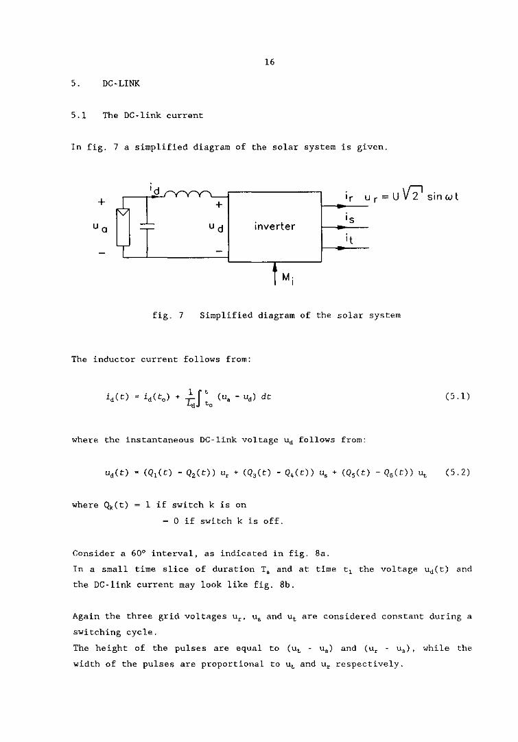
5. DC-LINK
5.1 The DC-link current
In fig. 7 a simplified diagram of the solar system is given.
'd r = U If21 sin w t + ~ yyy,--
'r U +
's =~ ud inverter U a
'1 ' t
-
t Mi
fig. 7 Simplified diagram of the solar system
The inductor current follows from:
(5.1)
where the instantaneous DC-link vOltage lid follows from:
(5.2)
1 if switch k is on
~ 0 if switch k is off.
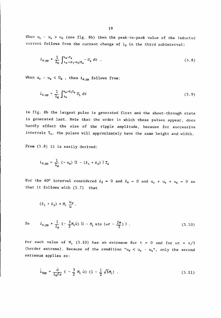
Consider a 60° interval, as indicated in fig. 8a.
In a small time slice of duration Ts and at time tl the voltage ud(t) and
the DC-link current may look like fig. 8b.
Again the three grid voltages u r • Us and Ut are considered constant during a
switching cycle.
The height of the pulses are equal to (ut - u,) and (ur - u,), while the
width of the pulses are proportional to lit and ur respectively.

t' -10 to
11T1J
I Us I I
60 0
• •
17
ud ---Ur-Us
- - - - - - - - - - Ud
to
I-I I I I I
I I I 6,T s ~ • • 6 T
1 S
•
fig. 8 Waveform of Ud(t)
The DC-link voltage ud can be split in 2 terms ud and ud defined by:
Substitution of (5.2) in (5.3) renders:
(5.3)
"d(t,) = ( (6 , (t,) - 6 2(t , ) } ur + (63(t , ) - 6 4(t,) } Us + (6 5(t,) - 66(t , ) } lit
(5.4)
Here 6k (t , ) represents the duty-cycle of switch k in the interval t, < t <
tl + Ts .
Assuming a symmetrical grid as defined by (4.4) and assuming sinusoidal
modulation according to (3.3) it follows from (5.4):
3 = - Hi U
.fi (5.5)

18
where U is the rms-value of the line voltage.
So, for a symmetrical grid and with sinusoidal modulation, the voltage
Ud(C1) has the same value for every switching cycle. For convenience of
notation we will denote ud(t) by Ud(t)
In steady state Mi will be controlled such that Ud = u. .
The lIaverage" DC-link current is gouverned by:
High frequency current component
For reason of 1) utilization of the solar array and 2) being able to give
limits for the continuous conduction mode it is necessary to have a
quantitative description of the ripple in the inductor current.
Because in fig. 8b both u(t) and o(t) are continuously changing. the ripple
in the inductor current will be a function of time. In particular we are
interested in the maximum-ripple amplitude and in the average-ripple
amplitude. Because of reasons of symmetry it will suffice to consider a 60°
interval of the grid voltage.
Consider the interval from fig. 8a
with ur = u sin wC
u, "" u sin (wt - 2,,/3) (5.6)
ut = u sin (wt - 4,,/3)
and ( °1 - °2) = H. u r , U
(03 - 02) = H Us (5.7) , U
(os - 06) = Hi u t
U
19
When u r - U, > Ud (see fig. Bb) then the peak-to-peak value of the inductor
current follows from the current change of id in the third subinterval:
(5.B)
When ur - Us < Ud . then id,pp follows from:
(5.9)
In fig. Bb the largest pulse is generated first and the shoot-through state
is generated last. Note that the order in which these pulses appear, does
hardly effect the size of the ripple amplitude, because for successive
intervals T" the pulses will approximately have the same height and width.
From (5.B) it is easily derived:
For the 600 interval considered 02 - 0 and 66
that it follows with (5.7) that
So 1 3· { L" (- -ZHiu) 1 - Hi sin (5.10)
For each value of Mi (5.10) has an extremum for t ~ 0 and for wt ~ 7r/3
(border extrema). Because of the condition "ud < ur - US". only the second
extremum applies so:
(5.11)

20
In the MPP (Mi - 0.822) eq. (5.11) reduces to:
with: U
Ld
fs
U 0.502 ..,.....,..." I"rs
rms line-to-neutral voltage
DC-link inductance
switching frequency
It can be shown that eq. (5.9) leads to the same expression.
Because discontinuous-conduction made will occur when
(5.12)
eq.
(5.12) can be used to specify Ld such that discontinuous conduction mode
only occurs at sufficiently low currents.
Note: The maximum peak current ripple follows from aiL/aMi = 0 where iL is
given by eq. (5.11). The maximum ripple appears at Mi - 1/)3 with 6, -
1/2 . so:
idpp,max U
0.61~ I,,"S
The ripple in the inductor current causes that the array current wonders
around the MPP. The average excursion from the MPP follows from the average
peak-to-peak current ripple "dpp :
6 Jn f6 idpp(wt) dwt
" 0
~ J'f6[ U (- 3 Hi) {1 -Hi sin " 0 Ldts 7
U 3 3 - ..,.....".. . - Hi ( 1 - - Hi )
Ld"s fi "
In the MPP (Mi 0.822) this reduces to:
( wt _ 2,,) "3
(5.13)

U >dpp/2 = O. 27 ..,.---,..-" LdLS
21
(5.14)
The average current ripple amplitude is approximately equal to Ldpp/2 .
So: u L dp =0.13..,...."...
LdIs
5.2 Required value of Ld
The value of Ld should be sufficiently large so that:
(5.15)
1) the invertor operates in continuous conduction mode at an insolation
of 10% of the maximum value;
2) the current ripple does not deteriorate the utilization of the array
with more then 1%.
sub 1): At 10% insolation the DC-link current will be 0.25 A. Continuous
conduction mode requires that the maximum current ripple amplitude is less
then 0.25 A.
So:
i dpp ---z<0.25A.
From eq. (5.12) it follows then:
0.502 U Ld > .,,---r-..,.,-= 2t,0.25
or: Ld~llmH.
sub 2): With Ld - 11 mH it follows from eq. (5.15) that
_ U - 0.13 ..,...."...
LdLs =O.13A

22
This means that the current ripple amplitude is about 5% of the full load
DC-current. Although this figure might be acceptable (a relative change of
5% in the solar array current causes a change in power of much less than
5%, depending on the particular array characteristic), an additional
capacitor is connected in parallel to the array, which further reduces the
array ripple current.
The main function of the capacitor is a snubber function. It deverts the
inductive energy from the DC-link wherever the DC-link is unadvertently
opened.
The value of C. 1.41/J.
5.3 High-frequency model of the DC-link side of the inverter
In the preceeding section the average peak-to-peak current ripple is
calculated. Although this ripple is cause by the composite voltage waveform
of fig. 8b, the ripple from eq. (5.13) can be considered as caused by a
square wave with an amplitude equal to:
3 (1 - - 11,)
" (5. 16)
In the MPP (M, - 0.822) this reduces to:
U d 0.54 U . (5.17)
This expression models the high-frequency voltage ripple which is caused by
the switching process.
Because of the following reasons the model is an approximation of reality:
the real voltage ripple is a function of time; the amplitude is
modulated with 300 Hz
the voltage ripple is not a square wave, but it is a composite wave,
Note that if we want to use harmonic analysis, it is advantageous to use
the fundamental of ud . For the fundamental amplitude goes:

23
So: . _ 12.f2 _ 3 ud - -_ Hi (1 - Hi) U .
'" " (5.18)
24
6. CONTROL
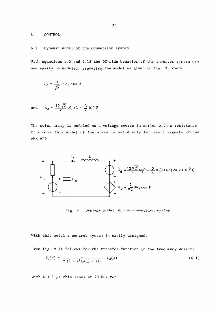
6.1 Dynamic model of the conversion system
With equations 5.5 and 5.18 the DC-side behavior of the inverter system can
now easily be modeled, rendering the model as given in fig. 9, where
3 - U Hi cos 4> .f2
and 12 .f2 H (1 - ]. Hi) U 1f ' 1f
The solar array is modeled as a voltage source in series with a resistance.
Of course this model of the array is valid only for small signals around
the MPP.
L + +
"0 +
fig. 9 Dynamic model of the conversion system
With this model a control system is easily designed.
From fig. 9 it follows for the transfer function in the frequency domain:
(6.1)
With C > 1 ~F this leads at 20 kHz to:
25
so that it follows:
i. ~ - 0,03 rnA
where: C -• 1,41 JJF
ud = 0,54 U (eq. 5.17)
U - 220 V
Ld - 11 mH
R - 135n
w - 271'.20.103 rad/s
Because of the presence of the "snubber" capacitor I the high-frequency
ripple reduction is more than sufficient.
Both the ECN-MPPT as well as the TUE-MPPT operate at frequencies below 100
Hz. Below 100 Hz the transfer function (6.1) reduces to:
For low frequencies « 100 Hz) we can also prove from fig. 9 that
With eq. (5.5) this means that the array voltage can be manipulated quite
straightforward via Mi :
3 _ H U
/2'

26
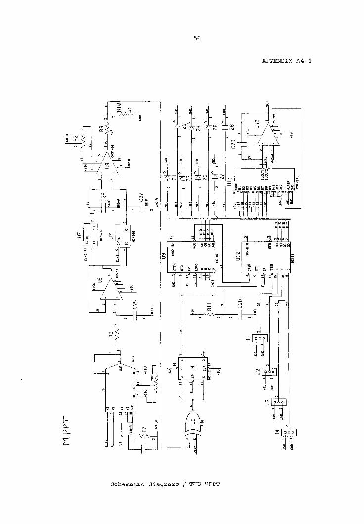
6.2 The TUE-maximum power point tracker (MPPT)
The function of the MPPT is to search for a set point of the solar array
such that the power which is extracted from the array is optimal, indepen
dent of insolation, temperature etc.
The MPPT is of a type which has no stable state; it is continuously
increasing or decreasing the modulation index Mi -
The modulation index is represented by the output of a 7-bit counter (see
fig. 10). Increasing and decreasing Mi corresponds to counting up or
counting down. Every clock period (10 ms) the counter either steps up or
down.
To control the counter the array power p. is sampled every 10 ms (synchro
nized with the utility grid). The power is obtained by multiplication of
measured values of the array Voltage U a and the array current iao
'a
multiplier sample and
holds
comparator counter
fig. 10 Blockdiagram of the MPPT
D/A M. ,
Note that the clock frequency of the TUE-MPPT is reduced after the first
test sequence.

27
7. HARDWARE
The block diagram of the system is given in fig. 11.
The system is contained in a 19-inch rack of double Euro-hight.
7.1 Power-stage
The power-stage of the actual inverter is mounted on two PCB' 5 which are
located on the front side of the rack. One board contains IGBT's 1, 3 and
5, while the other contains the switches 2, 4 and 6. Both boards also
contain output-filter capacitors, lGBT-drivers and snubbers. A LEM current
transformer which is mounted on one of these boards, is not used.
7.2 Modulators
modulator # 1
The modulator # 1 and the watching electronics are put together on a double
Euro-card. On this card a start/stop switch and some LED's are mounted.
This modulator consists of analogue and digital circuitry. The analogue
part performs the transformation of eq. (4.3) and the multiplication by K2
(see also eq. (4.7). The carrier u, is generated by a counter whose output
is fed to a D/A converter. The 8-bit counter is clocked at a frequency of
28 .20 kHz.
The carrier Uc and the signals u l , u2 and u3 are fed to comparators.
The binary signals generated by the comparators are input signals for the
digital part of the modulator, which is completely fit in an EPLD.
The digital part of the modulator is based on a state machine. After every
50 J.J.S interval the machine returns to a certain state. A change to other
states is driven by the comparators.
As indicated in fig. 5, each 50 J.J.S interval can be subdivided in 4 sub
intervals, viz. "shoot- through top", "first pulse ll, "second pulse" and
II s hootthrough bottom". These 4 subintervals correspond to states of the
state machine (there are some more states to reduce sensitivity to EMI). A
change to a next state is driven by the comparators (see Appendix Bl). Note

28
system with modulator # 1 s' '. ~' • ry-y-y-. Id
~ :1 l. o,~ o,~ o.~ I : r:
T 1 l. O2 O. O. • • •
I m-- (.0' .. '
~ .OO
po.t proc.uor •• 1
mo6ulotor ...... "'" rtr ... ' m, Jt-t=1::= WPP T .; ,
•
system with modulator # 2
'. '; ('Y"YV'I ~
~ :1 l.
0, ~ OJ~ O'~
1 ~ 1·; l. 0, O. o.
I
Cn--(.',. "
'9 .OO
po,l proc •• .or .1
modulotor b4.Gk~
~ I-+u,/,
LWOD r -'t-q~' Uri'#-.- MPP' «] • 0' • , •
c
c
..,. - .,
_I' • - b .,/j
I
......... • v ISV 12V (4.)
'2
b
......... , V .. v t2 Y (40)
'.-c ••
.(j .,/x
0'
11 mH
• 0,47 ~
, mH
• ,
l~. 2.a.7 mH C _
0,47 ~
fig. 11 Blockdiagrarn of the conversion system

29
that the indications "top" and "bottom" refer to the carrier being above or
below the sinoids in fig. 5. Within each state it follows quite straight
forward which IGBT should be closed, provided that u, is within the
envelope of the sinusoids.
When u, is outside the envelope a shoot through should be generated. From
inspection of fig. 5 it follows that the comparator that changes as the
second one after the start of a 50 ps interval, indicates which switches
should be closed to perform the shootthrough with a minimum number of
commutations. To make sure that the modulator operates well in the non-
linear region (Hi > ~ f3) , some additional states are defined.
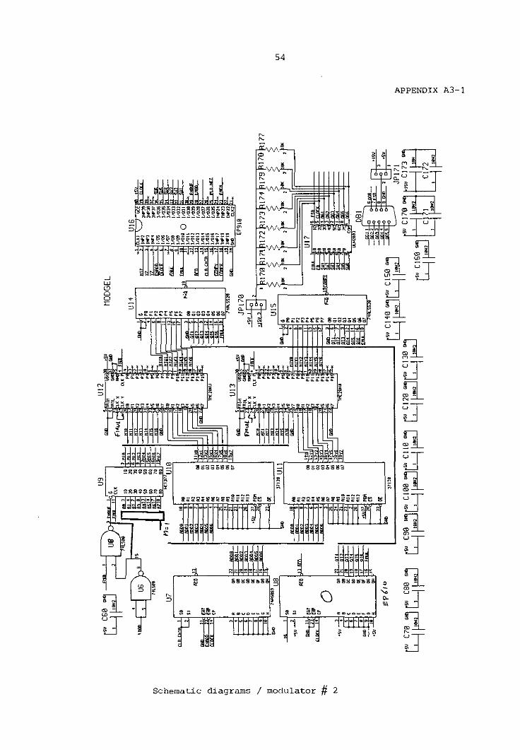
modulator # 2
Modulator # 2 is contained on a separate double Euro-card. This modulator
consists of digital circuitry and a PLL.
A block diagram of the modulator is given in appendix A-3.
Heart of the modulator is a ROM which contains data for successive on-times
of semi-conductors. Because each period Ts can be subdivided in three
subintervals, linking up to Ts ' onlu two numbers are required to indicate
the duration of subintervals. These numbers are stored in separate ROM's.
Successive numbers in the ROM which apply to successive intervals Ts are
addressed by a counter. The clock frequency of the counter is chosen such
that the ROM is read completely in one fundamental period of the grid. To
assure that the ROM is read at the same frequency as the fundamental
frequency of the grid, a PLL is used to lock both frequencies.
The numbers which are stored in the ROM correspond to Mi ~ 1. In order to
be able to control the modulation depth, the numbers which are generated by
the ROM are multiplied by Mi by means of a digital multiplier. The result of
the multiplication is stored in a buffer and compared with a (digital
representation of a) 20 kHz sawtooth signal. The output of the comparator
renders timing signals for the semiconductor-switches.
When modulator # 2 is used, the watching electronics is still required.
Modulator # 1, which is located on the watching electronics-card should be
made inactive, for instance by pulling out the driver Ie.

30
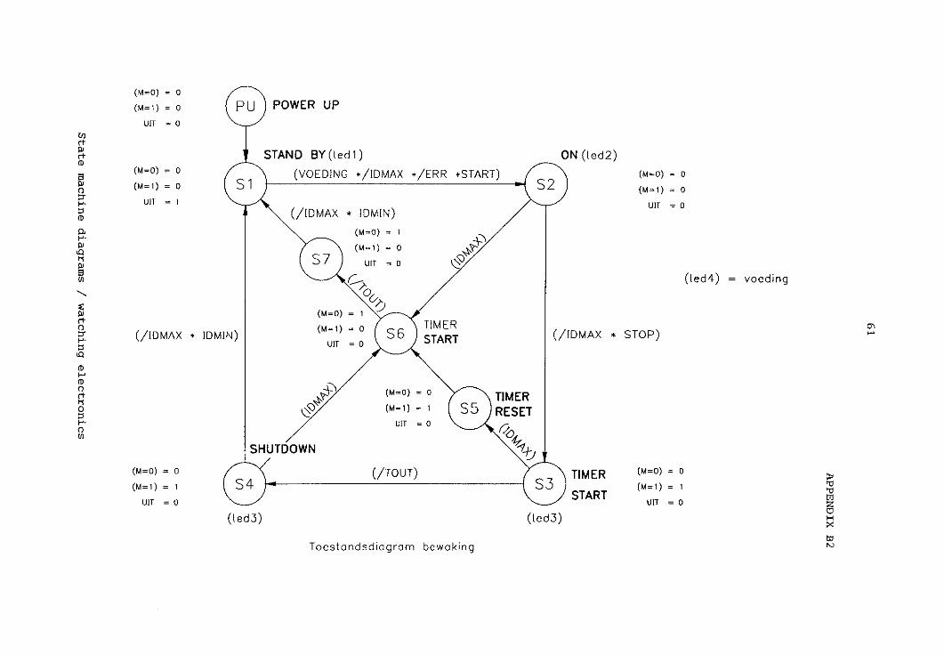
7.3 Watching electronics
The EPLD also contains the watching electronics, which is based on a second
state machine.
The watching electronics controls relais, it checks power on start-up, it
checks for excessive currents and it takes care of start-up and power-down
sequences. It generates some input signals for the modulator (Mi = O. Mi
- 1 , off).
States "stand-by". "on". IItimer start". "timer reset" and "shut down" can
be destinguished (see Appendix B2).
Change to a next state is either driven by the start/stop switch or by
outside events such as current sensors or timers.
When the start/stop switch is moved to "stop". the machine goes to the
shutdown state. In this state the modulation index is forced to Mi = I, so
that the current will decrease. When the current is sufficiently low, the
"stand-byll state is involved and all IGBT's and all relais will be turned
off (signal 1I0ffll is true). If excessive current is sensed, the machine
goes to the state, where all relais are opened immediately and where the
signal Mi ~ 0 is generated. The signals Mi - 0 is generated. The signal Mi ~
o forces the modulator to cause a shootthrough (via 1GB's 1 and 2). After
some time the stand-by state is invoked.
7.4 Auxiliary boards
The TUE-MPPT is positioned on the fronts ide of the rack. At the backside we
find the boards with external connections. The board with 5 plugs serves
the interconnection between the inverter, the solar array and the utility
grid. This card contains relais, fuses, filter F, the inductor L., capaci
tor Ca and two relais and two LEM's. One LEM (20 turns) serves measuring ia
for the MPPT. The other LEM (10 turns) measures id for purpose of over
current protection in the DC-link.
The filter F and some varistors are added to increase system reliability in
this experimental set up. They serve the suppression of occasional voltage
spikes which may occur in the utility grid. Because of the presence of the

31
output capacitors and the line inductances
superfluous.
these measures are probably
On the backside we also find two boards with power supplies. One board
contains 4 power supplies for the IGBT-drives. the other board contains
power supplies (0, +5, +15, -15 V) for the electronics and a +12V supply
for the fans. All power for these two cards is supplied via a separate
power card, and not via the plugs R, Sand T.
Note: the voltage measurements for the modulator and the MPPT is performed
via a resistive attenuator and are not galvanically isolated. The voltage
attenuator for the modulator is located on the modulator board.
7.5 Checklist for powering up and down
Turning on
1) Connect the power supplies to the AC-mains via a 220V power cord.
2) Check that the LED "standby" is on. If necessary turn the power
switch on the backside of the rack to "onll.
3) Connect the fans to the auxiliary 12V power outlet on the backside of
the rack.
4) Connect the phases of the utility grid to the plugs R, Sand T via
inductors of ca. 2 mHo Observe the proper phase order. )'
5) Connect the solar array to the inverter via 2 inductors of ca. 7 mHo
6) Move the switch on the control panel to "start". The system will
start after having checked supply voltages and current levels. Relais
will be closed.
') Improper phase order is not likely to damage the system; it will result in a phase shift between currents and voltages in lines Sand T respectively. Check for proper phase order in the following way: a) follow steps 1) to 4) b) connect a voltagemeter to the plugs for the solar array c) move the switch on the control panel to "start". If the DC-link voltage is negative, the phase order is not correct.

32
Turning off
1) Move the start/stop switch to IIstopll. The system will go to the
"shutdown" state, indicated by an LED. In this state Mi is forced to
one, so that id will decrease to zero. After a few seconds the sytem
will go to the "standby" state (LED) and all relais will be opened.
2) Disconnect the sytems from the mains.
Automatic turn-off
The DC-link current is monitored via a LEM by the watching electronics.
Whenever id exceeds lOA, even for a short time (for instance caused by EM
interference) the system is turned off by opening all relais immediately.
Grounding
The enclosure and the electronics GND are connected to the safety earth via
the 220V power card.
It is allowed to connect the plug marked N to the neutral of the grid. The
plug marked N is connected to the artificial center tap of the voltage
attenuator on the modulator PCB. This point is connected via a capacitor to
ground.
33
8. TEST RESULTS; OBSERVED WAVE FORM DISTORTION
8.1 Test results
Although the system will be thoroughly tested at ECN, some test results are
shown here.
The following set up for testing was used:
+
inverter u
fig. 12 Test set up
Waveforms are shown in fig. 13 to 16 for the following combinations of
voltages and currents and modulators. The MPPT was present.
fig. u. i. C modulator line filter
13 500 V 2,34 A 4xO,47 J"F # 1 yes 14 500 V 2,34 A 4xO,47 J"F # 1 yes
15 500 V 0,0 A 0,47 J"F # 2 no
16 500 V 2,3 A 0,47 J"F # 2 no
For all figures:
rms grid voltages 229 V
Rr 130 (]
u. 500 V
L, 950 J"H

34
Jet. v 3.IlUlI mV v
-;::8;' 0 2. aUf!
~'!"I~~M~~¥\.)~~~~~ mV V
101. 0 i, B08 _ .V v
u~ .... ~ ~
Sl.no 909.0 "'IV .. '/
1°,00 ·1!1.?Cl ,', mV
11 11,[1 1. Hl~. mV \'
-?I!1.{J "!. 1~(. ~'; V
-319, U -1.192 m'l '/
"09,0 -4. ttl:::'. ,'I 'I
I L.= 3.9G9 m:3 11.90 as 19. 84 IllS 27.77 IllS 35.71 11:5 3.9GS mS 11.00 IS 19. 83 .S 27.77 !lIS 35.70 liS
fig, 13 Voltage u. and current i. (2A/100mV) (modulator # 1),
95.60 190. ~ mil 11'1
70.60 140 . .4 m'l mV
45.60 90.40 JIlV mV
20.60 40.40 mV rrIV
.. 4. 400 -9.600 rI'l ='1
-;"''9. 40 ··59. 60 .'1 mV
~5.t. 40 -109. 6 Ifj'l rII'l
-79.40 -159.6. mY /DV
-\0\.4 -209.6 fJ'I Ill"
L..==: 3,958.S 11.90 rtS 19.84 as 3.965 liS 11. 90 1115 tn.83 illS
fig, 14 Line voltage ur and line current ir (2A/100mV) (modulator # 1)

" ... 4~ L, "r '11.11'1 '1.'1," IL'II \. !}f!~ ., • .. • J,'. [Ill! ?.'If>G :;~. 211 1.1!14 ~V I V •• •
,
~1.1l1l1 UJror, 29.;>U •• • ••
:>;'. !~l Qf,{;.O <.;>m . , •• •• ~.1fX1 1U~1 ;>1l.!~1 •• .. •• ;>/.?!l um (5.01'1 •• • ••
.r,z.20 2.014 70. 9:1 -1.016 •• • •• • lI.{!) -3.014 !l'i.Rr1 -1.~16 •• • •• • IlL'.? 4.U14 l?1J.H ?mf, ~vv.vv ,
'~----,...-/
~.!i,9~ J.!I6J ~S ifl.ls .5 .
__ -.1:~~'~
fig. 15
35
II"
o A (modulator # 2)
-. :rio /1 II'j
~,./1I .s 3'.i 70 ~~ ?" 711 ~~
fig. 16 Waveforms of U a • i a • ur and ir at ia - 2,4 A (modulator # 2)

36
From fig. 13 it follows that with modulator # 1 the DC-link does contain a
ripple component. The ripple consists of components with frequencies n. 50
Hz. The magnitude of the ripple cannot be clarified from the distortion in
the AC-line voltage, so that it is probably caused by the modulator.
From fig. 14 it follows that current components of nature a, band c (see
section 8.2) are
present in the AC line when modulator # 1 is used. The phase shift between
current and voltage is caused by the output in capacitors (4xO,47 ~F). The
large distortion in the line current is caused for the major part by
inaccuracies in the modulator. Current distortion of nature b is small,
because the AC voltage in only slightly distorted.
8.2 Line induced DC-ripple
In chapter 5 the high frequency ripple in the DC-link was considered.
Symmetrical and sinusoidal grid voltages were assumed so that no harmonics
of 50 Hz would appear in the grid and in the DC-link. However, after the
first test, harmonics were observed. This section deals with harmonics in
DC- and AC-1ines.
At constant insolation the solar array will produce constant power when it
is operated near the MPP, so both u a and ia will be constant too.
The principle of the modulator # 1 is such that the instantaneous phase
currents are congruent to the phase voltage (provided that Mi is constant).
For a symmetrical three-phase system with sinusoidal voltages, this means
that the power which is tranferred to the grid is constant in time. For a
lossless converter this will mean that the power which is extracted from
the DC-link is constant.
However, if the phase voltages are dh.torted, then the currents will be
distorted too. Without proof it is stated that this will result in a (n. 50
Hz) ripple in the DC-link current.
(Note that it follows from (5.4) that for non-sinusoidal voltages eq. (5.5)
is no longer valid; ud will contain a ripple component.)
Because the inverter can hardly store any energy, a variation in DC-link
current will result in non-optimal utililization of the solar array.
Depending on the local quality of the grid, this problem may become more or
less serious.

37
Possible measures to reduce the AC waveform distortion:
1) By a fast control of the modulation index Mi one can generate an
"anti-distortion ll of the current such that P is still constant. From
a fundamental point of view the TUE-MPPT is suited for that purpose.
However because of the low clock frequency of the MPTT. the modu
lation index cannot be controlled fast enough. One could try to
increase the MPTT-clock frequency up to about 1 kHz. Note that at 1
kHz eq. (6.2) is not an accurate approximation of (6.1). (On-board
unused IC's are present for that purpose.)
2) On basis of the concept of instantaneous power control one can
calculate the 6' s such that the instantaneous power is constant,
undependent of the shape of voltage waveforms. The development of
such a control unit, based on a DSP, can be a subj ect of future
research.
3) Usage of a different type of modulator which uses a precalculated set
of 5's. See sections 4.2 and 7.2.
Note that all solutions will give rise to harmonic line currents when
harmonic line voltages are present.
The largest contribution to the low-frequency ripple component in the DC
link is probably caused by non-linearity, inaccuracy and noise in the
analogue part of modulator # 1.
In relation to eq. (4.11) it has been proved that modulator # 1 will
operate in linear mode for M, < 0.866. In the MPP the modulation index is
expected to be 0.822 at a grid voltage of 200V and cos '" ~ 1 (Note:
3 Ud = - Hi U cos'" )
{i
Due to a) a low line voltage. b) cos'" < 1. c) the searching process of
the MPTT and d) inaccuracies in modulator # 1 it may occur that Mi exceeds
the volume of 0.866. In the non-linear mode the modulator will generate
distorted currents. giving rise to a ripple in the DC-link current. This
may reduce the utilization of the solar-array. When these problems are
serious one may consider to reduce the number of panels in the array.
In fig. 13 and 14 waveforms of the DC-link are shown.

38
8.3 Harmonic currents and voltages in the AC-line
In the lines which connect the inverter with the utility grid, harmonic
currents will flow. Several components can be distinguished:
a) high-frequency components caused by the switching process
b) harmonic currents caused by the presence of the output capacitors in
combination with a distorted grid voltage
c) harmonic currents which are caused by modulator # 1 and which are
rooted in either the harmonics of the reference waveforms or in non
lineary and inaccurary in the modulator electronics.
ad a) High-frequency currents caused by the switching process.
Consider the inverter as a current source i; which generates both
low and high frequency components. To calculate the harmonics caused
by the inverter, the model of one phase, according to fig. 17 is
used. A line inductance L1 is assumed. The capacitor C* represents a
center-tap configuration of C's, so that
C' C/3
where C is the capacitance of the delta-connected capacitors.
• I I r
c·
fig. 17 Model to calculate both high and low frequency components in ir
The pulsating current approximated by:
(8.1)
This expression reflects that the line ripple currents is modulated
in amplitude with a frequency 6 Wo

39
To calculate the average high-frequency current ripple in the utility
line, eq. 8.1 can be approximated by:
From a Laplace transform of i; ir and ur it follows:
(8.2)
and U' (5) _ SL Ir' (5) r 1 ~ 52LC"
when (8.3)
From eq. (8.2) it follows that it is required to have an inductance
in the utility line. An inductance of (at least) 1 mH is recommanded.
Eq. (8.3) can be used to calculate the ripple voltage on the output
capacitor C*.
For fs - 20 kHz, L - 2 mH and C' - 0,47 ~F we find:
or (8.4)
ad b) Harmonic currents caused by the capacitors which are connected to the
grid.
The harmonic currents which are caused by harmonic voltages in the
utility grid, can be calculated with the model from fig. 17 too.
Again the model represents one phase of the grid. Note that these
currents even flow at no-load. They can be superimposed on he cur
rents which are generated by the inverter.
The harmonic currents caused by harmonics in ur follow from the
transfer function:
when I; - 0 .
In general low frequency (250 Hz, 350 Hz, etc.) harmonics are con
cerned, so that we find with C' - 0,16 ~F and L - 2 mHo
(8.5)

40
Apparently the inductor does not affect the low-frequency current
components. To reduce the harmonic current, the capacitor should be
chosen as small as possible from the viewpoint of high-frequency
ripple reduction.
Because the inverter is designed for 5 kVA, the capacitor is rela
tively large, thus giving rise to relatively large fundamental and
harmonic current of capacitive nature.
Note that it follows from eq. (8.3) that the magnitude of the fun
damental capacitive current component is appro}:irr.,tely 0.5 A at C = 2
~F or 0.1 A at C - 0,47 ~F.
To reduce the harmonic currents it is advantaeeous to reduce the
output capacitor value. Fig. 15 shows ir at ia = 0 A, with C = 0,47
~F. A significant amount of low order harmonics can be observed.
ad c) Harmonic currents generated by the inverter with modulator # 1.
As stated in relation to eq. (4.4) currents i' which are generated by
the inverter are congruent to the voltages when modulator # 1 is
used. When the line voltages contain harmonics, the current will
contain harmonics too.
(AI though the line currents should be proportional to the line
voltages to obtain unity power factor (according to modern defini
tions), not all people consider the proportionality between voltages
and currents as an advantage.)
A quite different source of harmonics in the currents is rooted in
the electronics itself. Due to 1) inaccuracies in the electronics
(such as unequal voltage attenuators, offset, drift), 2) non-line-
arity of the modulator and 3) l.vise, modulator # 1 may generate
control signal which give rise to harmonics in the line currents.
A way to obtain inverter generated sinusoidal currents is to use a
different type of modulator. When modulator # 2 is used, which reads
pulse pattern from a table, the grid voltage and noise will have
hardly an effect on the currents generated. Note that this solution
will also give rise to a (small) ripple in de DC-current (see section
8.1) due to harmonics in the line voltage.

41
From fig. 14 it can be concluded that harmonic components of nature
a). b) and c) are present when modulator # 1 is used.
Fig. 16 shows that, with modulator # 2, the current wave-forms are
improved. At full load the harmonics are reduced to at least -30 dB.
However residual harmonics are still present. Low order harmonic
currents are probably caused by harmonic voltages in the grid (see
fig. 15 also).
In Appendix D some spectra at full load are shown. both on linear and
log scale.

42
9. POWER CONSUMPTION AND EFFICIENCY
In the introduction it was mentioned that the inverter system was primarily
intended for powering AC-machines. For that application a high efficiency
is desired from the viewpoint of being able to remove heat. The consumption
of energy, including the power consumption of control electronics is mostly
not a matter of merit.
For photovoltaic-conversion systems the consumption of energy by the system
itself is a primary matter of interest. In particular at partial insolation
the power consumption can be a substantial part of the output power of the
array. For a certain required power output an increase in power consumption
means an increase in solar-array area, where we should bear in mind that
cost of the solar-array dominates the system-costs.
As stated before the power consumption of the electronics and the power
loss in the inverter circuit was not optimized. In table 1 the estimat_ed
power consumption is given. In the second column it is estimated to what
level the consumption/loss can be reduced in a dedicated design.
estimated power
consumption/loss
ac- fea-
tua1 sible
drivers 5 W 1 W
power supplies + 32 W 10 W
control
fans 10 W 0 W
relais 18 W 1 W
snubbers 2 W 1 W
semiconductors 40 W 40 W

43
A large reduction in power consumption can be achieved by redesign and
optimization of the auxiliary hardware such as drivers, power supplies.
fans and relais.
The power supplies which are used to power the IGBT-drivers are quite
oversized. By using efficient power supplies of adequate ratings, the
consumption can be reduced substantially.
Under normal environmental conditions the fans can probably be turned off.
The fans are electronically controlled. At high temperatures the con
sumptions of the fans will increase. Replacing the electromechanical relais
by solid state relais will reduce the power consumption dramatically.
Because the semiconductors are oversized, it is to be expected that the
losses in semiconductors will increase if smaller ones are used.
Although, from a fundamental viewpoint, less than 10 mW is required to
drive all 1GBT' s, it seems practically feasible to create drivers with a
total power consumption of less then 0.2 W
each. Replacing the resistors which are in parallel to the gate-emitter
connections by active
non-dissipating circuitry should give a major improvement.
The snubbers were designed for a 5 kVA power module. Because only 1 kVA of
power is converted, it is allowed to reduce the snubber capacitor by a
factor 5, thus reducing the snubberloss substantially. The value of dV/dt
will stay within safe limits.

44
10. CONCLUSIONS AND FINAL REMARKS
The following conclusions are preliminary. Final conclusions can be made
after a thorough testing and measurement program has been carried out by
ECN.
1) The PWM-CSI is able to convert DC-power to the utility grid at a high
efficiency.
2) The output capacitors of the 5 kVA inverter stage have a low im
pedence for harmonics in the line voltages. In order to reduce
harmonic currents the output capacitors are reduced from C = 4 x 0.47
~F to C ~ 0.47 ~F.
It is recommended to measure the harmonic distortion of the output
current of the inverter at in stand-by state, in order to be able to
quantify the currents of this nature.
3) A reduction in output capacitors will reduce the capacitive component
in the fundamental.
4) Because the impedance of the grid is relatively low it is required to
use inductors of ca. 2 mH in between the inverter and the grid in
order to block high-frequency (20 kHz) currents which are caused by
the switching proces of the inverter.
5) Theoretically, usage of modulator # 1 (triangulation method) causes
line currents to be generated which are a linear mapping of the line
voltages. This means that, theoretically, power is transferred at
uni ty power factor. An advantage of this modulator is that when
voltages are making a phase-step the currents will make a phase-step
too, thus continuing power transfer.
Modulator # 1 is linear up to Hi = i .[3 .
6) The modulator # I is not operating well. Harmonic currents are
generated because of the following reasons:

45
a) when Hi > i 13 the modulator operates in non-linear mode. Due
to the searching proves of the MPPT the modulation index may
frequently exceed this value.
b) due to harmonic line voltages, harmonic currents are generated
because references for the modulator will contain harmonics.
This contribution is supposed to be small.
c) due to inaccuracies and noise (EMC) the modulator generates
improper signals which are not in accordance with the reference
signals.
7) When sinusoidal output currents are desired (even at distorted
voltages; in that case pf < 1 I). modulator # 2 should be used. This
modulator reads precalculated pulse patterns from a ROM.
8) The conversion system with modulator # 2 is operating better than
with modulator # 1. Residual harmonics are still present « -30 dB at
full load ). even at no-load.
46
11. REFERENCES
[lJ De Haan, S.W.H. and A.C. Blom,
AN ULTRASONIC SWITCHING CURRENT SOURCE INVERTER WITH IGBT'S.
Proc. Int. Power Electronics Conf. (IPEC), Tokyo, 2-6 April
1990. Vol. 2.
Tokyo: The Institute of Electrical Engineers of Japan, 1990.
P. 841-847.
[2] Nonaka, S. et al.
INTERCONNECTION SYSTEM WITH SINUSOIDAL OUTPUT PWM CURRENT SOURCE
INVERTER BETWEEN PHOTOVOLTAIC ARRAYS AND THE UTILITY LINE.
Proc. Int. Power Electronics Conf. (IPEC), Tokyo, 2- 6 April 1990.
Vol. 1.
Tokyo: The Institute of Electrical Engineers of Japan, 1990.
P. 144-151.
[3] Teng, M.H.T.
EEN MAXIMUM POWER POINT TRACKER: Een rege1aar ten behoeve van een
zonnepaneel (in Dutch).
Vakgroep Elektromechanica en Vermogenselektronica, Faculteit Elektro
techniek, Technische Universiteit Eindhoven, 1991.
Stageverslag EMV 91-02.
[4] De Laat, R.F.C.
EEN PULSBREEDTE-MODULATOR TEN BEHOEVE VAN EEN STROOMCONVERTOR.
Vakgroep Elektromechanica en Verrnogenselektronica, Faculteit Elektro
techniek, Technische Universiteit Eindhoven, 1990.
Stageverslag EMV 90-08.
i. ~ • • ~ ~
2' ~
'" <
'" u 18(1/;; u I
15"(
:;: ~ '"
• i. • • " ~ , u; '" u
47
a9S
aos
N ~
'" u
~ ~
i ~ . '" ,
V0
I va l.a
i
circuit . diagrams I power Schemat~c
APPENDIX Al-l
, ;
Hf .~
48
APPENDIX Al-2
"' ~ ., VA
"' U
ISO
~~O 0S5 ISS
• ;;; • ~
~ ; " N
~. M
~ ~ ~ llSr'I U ~ "' "' U u ,
~ 1£0 ZOO • • ; I
N .>'1ll:1r'1 ~ ~
~ ~ U U r
BES IE5 ZES ££5
rI} ,~ ~ ..
t ~
" ~ ~ N I
~ s: VV\ "' "' IS'tIrI ~ ~ ~
w ~ ~ U U ( 0- i ~ '~ ::.:: " .
• ~ 110 llO ~
~ ~
• 115 ZIS EIS
Schematic diagrams / power circuit

en o :r
~ n.... o 0. ....
~ ~ '-
8 0.
" .... ~ no ~
'It: ~
BEP~lJNG U, ,Ul EN UJ UJ ,Ul EN U3 ~ DE NDDUlAriEINDEX VEtl..GEli.Jl'<iN(' VAN Ull(r1i,
U2*Mi EN U3*Mi MET Uc
I R10 XI U7 Z [,'SV 330k R15 Ul 12 xl \ II
~30K em\? IIIIMI 5" '-..._
U3 " ",,·R . ....:::::
"U 4 U~OISI -U3
I PD€i32 C~T' UI3L9H
ISU ISO 3 L-..!..foo-t'--+=-f '50
2 P70 0
"'''' , I'" :::: R30
~
"r'"I21.prt·
R16 , "
100< .. 1&.1
R14 2 7 ,,-'
r /
1'50 <: R31 .. I, ,
I" , " , '->-~"~~wc-t-t----~----J "'1\17 ,Ul
;:. j~~ ''''
'- III 001 Ie _ '-~ ........
U3 Ct'P2
Gt() .. v U-OS -0 f'OS32 9.. LM3L9N
Ii II 3 /r' ~ I - v'>
USIX ,
" .. ""'·R
''''
-ISU
"rt24.prt '
R22 foo(\J\J\-2
R21 t ~~3 R26 U2
R27
"SVWP20
"rt 24. pr-t2
" f]
1-'11':> , 2
"
)SV ISU 8
"" "rt2i.prt"
,50
r"" I 1""111 5 r,t' .. U4 ~2
'a/lM""" , ' '50
"'
, I'" S R40
'''''
~
i;; 'd
'" B H X
!I> N 1 ~
'" '"
til ()
::t
~ rt ~.
o p, ~.
0>
'" ~ ~ "-
5 p, c .... 0> rt o ~
:;:, ~
8EPAliNG URN DE MODULATIEINDEX
'W
R42 ['W
MI
R23 V·/\
t'w '~R4I t:W
, ' 'I R2~ -', t4 - . 1 I. 'V\~ U2 :;:r--
• 1'l:J:tl:':;'~ ::: -'~ 'tt" -1\\1 ~ ,
Ri3 C 19.1 J
DRI43 .> <'
, I'"
" •
,~
RI42
.. , t1111 to cHI zlJ" optloneel
~ ~P21 "rt2'1. prt" 1.
.!!ll
."" '" DU'IS
.OlY 61
.SEIl W.rt
.s:EH W.Dl
nOHS
""
Vc>£.OiNt; SpJ'HJNiNC, ~.EwA~tNS
+C143
] "'<:~It-u.p"'! ....
f" ~~~ RI H
2'ftl.8
:!.IS
OPUEKKHlG 2AAGTAND UC
.. • • .. ~ TIl: ~
"' -~" "W 1 [?1r-
"
1M I: i?!
"" AW2
-~ RUIl
-
'''J RI54 J RI52
2 ill~ 2 hili::
dS@ en CISI tljn .. ptlo ..... '
'"'
"tJ psral~2"""T' '1-I_~
R50 111:11(
R52 'V'/'. 1 I n I 'I ,.
f3
.!!.!i .OFIIJ U() .IllY 61, .SEN W.I~ .SEIl W.OL
r1C3H5
..
-,.
'50 ·1 %R151
2<1&108
:» "" "" '" 13 H X
:» tv I
tv
Ln o

OPWEKKING
P 113
PULSPRTROON
B6 A7 AS A.
" lS lS "
sa A9 89
AI" AJ 'Ie A2 '11 " CII '1 cle
e> Oil CI ole 02 'II 01 'II 'I 'Ie
F> Gil 'I HII GI Hie H2 JII HI Jle
J2 'II JI 'Ie 'I lie K> 19 l2 K9 K3 La L3 " K1 l7
11m GHOI lICe> GND2 vee3 GNDJ UCC1 OND1
EPt1S12B
51
Jl
GHI)
APPENDIX A2-3
+5U
R160
2
R161
R162
RI6~U ;>--''---+---+----j----+-, 1<, R 1 64
17
7
"" (D
N
Schematic diagrams / modulator # 1
."
tSU I
52
STAAT/STOP CIRCUIT
11 sunCH
"" ,
CI 70 +
, l
SU ""UoneR' p .... 2 • 13 .... 19 • 5 uordotn QP dII print door ..... bond.n. RI71 .... ~171 ~;jn uel ~ ••
R}70 lllut~t.
UI7
" Q'
" CEXT
'''' 71LS2Z1
"<;ue-. '-"
RI72
UI7 ,
" , " Q, , , CEXT
"" 71Lsnl
'ORI74
C7171 + -"UI-••. prt"
OPWEKKING CLOCK F0
U13
CI30 --' , " HN"
" , .. , '" " XTfJ..1 " Fe '" " XIAL2
" '" '"
+'~31 =& s '" FFQ 1
71lS3Z1
APPENDIX A2-4
BEWAKING TUSSENKRINGSTROOM
AG0 .... ASI :r,jn opHone .. L alSO Rse;~ ..... ou ..... bruQt. GO-A." GO zljn blj hQt Ie
3 (LMJI91 doorverband .....
P60 2 ~10l< "RT21.PRY-
R66 ,,. , r---'- -,
I ~61 I G
11-~ ~ R6?
2 12'1 ~32139K t{)-A ~-R
0"" 3 ~~~URT'
, > 50k , 2
R63 2 p9K
~--+--"~'--1-
+ISU
"
Schematic diagrams / modulator # 1

53
APPENDIX A2-5
"fl'"1e.pr-t·· "f 1 'leo prt .
r.TI1 < ~ R2 ('Rl -~ .< . /
6nF <212K 6nF < 212k 2 2
---
,~----t------r--~r-------t---i.~/X t---~-------r---r-"OII~
UT!X
--
"r-Se.prt"
--
Il5 18°1' 8k7
STERPUNT "r-6e.prt" "1~6e. prt"
~0nF ~ND
Schematic diagrams / modulator # 1
54
APPENDIX A3-j
Schematic diagrams / modulator # 2

55
APPENDIX A3-2
~
~
• ~ ~ ;Ll M - N-
-~iIT a::U U
'"? ~ -
;Li ~! -! ~ ~""", 'J3r ' -
~
V\" => .. • a • a "' -i IT w IT '" " r< 0 ~
>= ::; a ~
IT a IT a IT a IT a IT !"l '" 'J
lIiSl!l8~1!J8 !JL ro
:l 'J GO -
!JL <.0
'J ~ ~
'J
Schematic diagrams / modulator # 2
56
" ~ i! => ;;
• ~ ; e
. en => • , ~ "''''UO
, a: ~/VV\ N
• ~ • T .
~ => d
" ~ ~ . , • 0
"-,
TUE-MPPT diagrams / Schematic
en N U
APPENDIX A4-1
il
~ / ,
§
•

til o :T ro ~ rt ~.
o p, ~.
0>
'" " ~ '>,] c
'" I :;:
'" :'l
0:;1) Ib.. C.LoG\,( T BV. I""IPPT '<1fT If~T NET (, TO < '/ N (liP. (.'( / / SF- E po!)£:
2
I
<-PI~
CI : ~ II 1
<: RI
~~7 2 3 2. "-
UI Gt()-R J + /rJ ""'" /J .' I .
I I+SU
t'5O ~ R5 '--l J PR a , ' - ....... R4
c{:CP
U2 ~9:IV~ I." '-ll,""6" I 6. I J r-I, '"
, II 1 2 Q 1
ISU R2
~_-'2...J1~·L i~ "'66
J50
;;: R6
C3 a
-50 R3
150
,------,_---.-_---,-_,---,r'-"+IS"'-.1I ---, -511
.1 C4 :1 C5 :1 C6 :1 C7 :1 C8 :1 C9 :1-C30 .i Cl7 :1 Cl8 :1-C32 1 ! I I I ± J---T T M T---, 2 CI0 ~ CII iCl2icI31cI4~':-:51C31 .i C21 :1C22 :1C23:1::'4 -;r -;r -;r T I I-IS" fCAS£o.,·p"'T T T T ,,~
CP U4
t.... __ ...... H Q ~6
~ '" ~ H :>< ~
"" I N
en ...,
r-''--
6
In L~
~ .
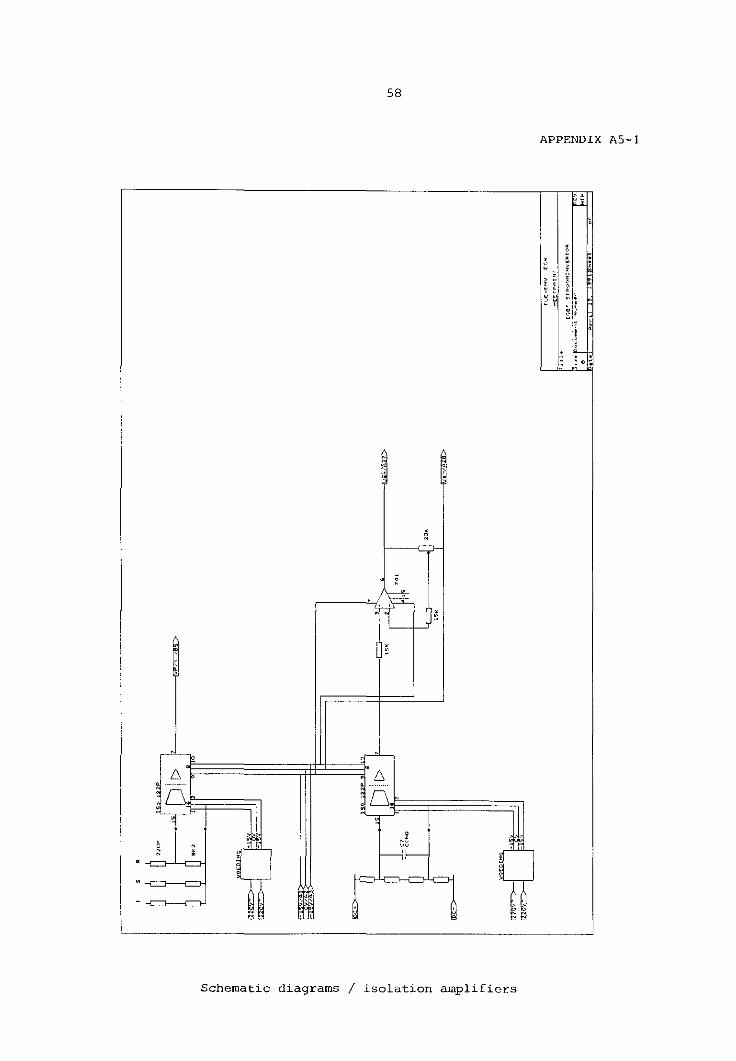
58
<--,i-
6
In '--c,---
~!
Schematic diagrams / isolation amplifiers
APPENDIX A5-1
i ~ ..
~ ~ '" ~

59
APPENDIX A5-2
::i "
:
" > i , , I , ,
1 I!- • . . . -
, , Lf-.-~~ ~
,~
"Z,," ~ ("~"ZOp
I -- I -~
I , . ' . • i
I
:'if-I
I
I j
, :1 I r :"',./;'< " ,
! I 0
'JJ/'
i ~
Schematic diagrams / isolation amplifiers

til rT ~ rT ro
~ n :Y ~.
~ ro C, ~.
~ cO ~
~ ~
'-
8 0. ~ >-" ~ co " "*
(jM~O • 5C~0) B3 B2 B 1 BO
UM~O * /5C=0)
(TIMER) (M~O)
(TELLER 1 )
2 set 0001
(5C=3 + SC~O + TELLER)
(jTlMER + UIT) (/TELLER 1 + UIT)
T oestondsdiagram modu\otie
(5C~0 + SC~ 1)
(SC~2 + SC=3)
4 set 2 0010
(5C=1 + 5C=2)
~ " '" 5 H X
'" -
'" o
(M~O) ~ 0
(M~l) ~ 0
UIT = a
PU POWER UP
STAND BY (led 1) ON (led2)
(VOEDING ./IDMAX ./ERR .START) (M~O) ~ 0
(M~1) ~ 0 Sl S2 (M~O) ~ 0
(M~1) ~ 0
UIT "= 0 UIT = 1
(jIDMAX * IDMIN)
(jIDMAX * IDMIN)
(M~O) ~ 1
(M~l) ~ 0
un ~ 0
0. °u Q (M=O) = 1 _________ .,
S6
:0 (M~O) ~ 0 ~'<-
I§J (M~l) ~ 1
UIT ~ 0
SHUTDOWN
(M~O) ~ 0 (jTOUT) (M~1) ~ 1 S4
UIT ~ 0
(led3)
T oesta ndsdiagram bewaking
(led4 )
(jIDMAX * STOP)
TIMER RESET
I/O ~ '1-f)
TIMER (M~O) ~ 0
(M~l) ~ 1 START
UIT ~ 0
(led3 )
voeding
;p
'" '" '" Z tl H
" "' IV

MAX+PLUS Compiler Report File Version 1.51 3/8/89
62
***** Design compiled without errors
Title: EPLD-MODULATOR company: TUE-EMV Designer: BEUZEKOM-THIRION Rev: A Date: SEPT.1990 Turbo: ON Security: OFF
C 0 U N T 5 0
C 0 U N T 4 0
C e 0 0 U U N N T T 3 2 0 0
e e 0 0 U U N N T T V 1 0 e 0 0 e
APPENDIX Cl
A: \MOTOT . RPT
R E S E
0 U R G G G G 0 U V V V N F N N N V V 1 1 E D 0 D D D 5 5 5 5 D
-----------------------------------------------------/ 9 8 7 6 5 4 3 2 1 68 67 66 65 64 63 62 61
COUNT60 10 60 RESERVED e10 11 59 RESERVED C20 12 58 RESERVED
CMP1 13 57 RESERVED RESERVED 14 56 RESERVED
CMP2 15 55 RESERVED GND 16 54 vee
eMP3 17 53 RESERVED C30 18 EPM5128 52 RESERVED
RESERVED 19 51 RESERVED vee 20 50 GND UIT 21 49 Q10
MISNUL 22 48 Q20 MISEEN 23 47 Q30
IDMAX 24 46 Q40 IDMIN 25 45 Q50 START 26 44 Q60
27 28 29 30 31 J2 33 34 35 36 37 38 39 40 41 42 43
S S S E R G G G G G V L L L L L R T 2 3 R E N N N N N C E E E E E E 0 B B R S D D D D D C D D D D D S P E 5 4 3 2 1 E
R R V V E E D D
EPLD / pinning
CMP1 CMP2 eM?.:! Fe
. . L: . ,
5TAFIT ~"~UT
STOP ,. ,
ERR eyo ,. ., OYU5 'N;'B ... uyo UV1~
lOMAX ,. ,
IOMIN ,. ,
~
1 .... uT , ,.
IGBT MODULATOFI of- BeVe1't..·~~
TUE-EMV
8EUZEKQM THIRION c, • . . ,
FF
63
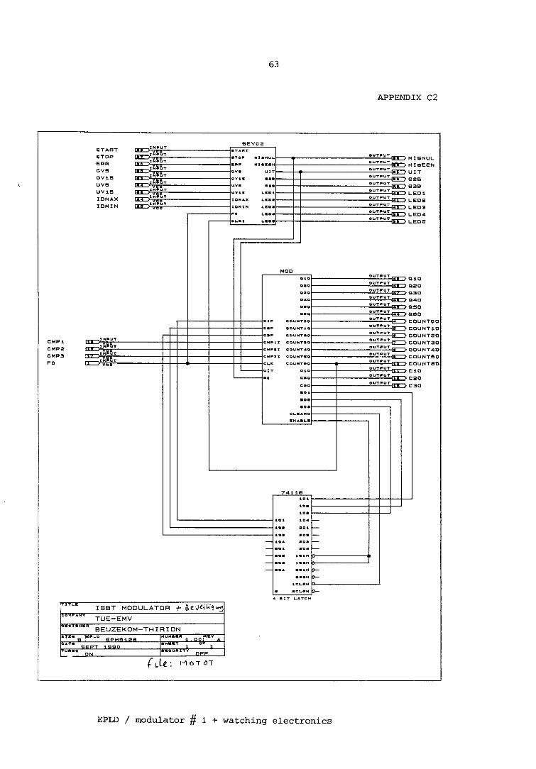
BEYC2
aTOP "laHUL
10 ......
"" aVLCI ... to ..... )!
10"lH LEo. ., La,," .;a.IH La,,_
"""., " ..... 1
" ..... 1 .c. '-- ." .,
---
=
MOO ,., ,., ,.,
,., ,.,
"OU"TOO
O ...... ~T~O
CO .... T80
" .... NT .. "
" .. UNT""
CO"'NTal;> .. , ••• ... ... . ,. u •
• " ... La
74115 ., . . ,. ".
EPLD / modulator # 1 + watching electronics
APPENDIX C2
OUTpUT MISNUL
guTI'''T MISEEN un sao
ouT" .. T sao guT""T
LEOS. OUTPUT
LED2 OUTPUT
LEO:;! ouTP'U'r
LE04 OUTPUT
LEOO"
OUTPUT 0'0
IIUT" .. T 020
OUT""'!' cae ouTPUT o.e OUTPUT C.O DUT," .. T
CSO ouTPuT COUNTeD ouT""T CQUNTiO CUTp .. T
COUNT2D OUT""T
COUNT.30 gUT"",!,
COUNT40
COUNT!lO
COUNTSO oUTPUT c,e OUTPUT cao OUTPUT cae

BEve:!. START IN .. UT
.T .... T MI.NUL. OUT .. UT MISNUL
STOP ERR
, "' .To" MI •• IIN OUT .. UT MIBEEN , " ... m OUT .. UT UIT
'" OVO
'" OVle
, , .n ... OUT .. UT S2. , , ov ... . .. OUT"UT S'.
t-< UVO 0 UVle
, , ",. I..II0l OUT .. UT LEO:!. , ,
u .... 1.. • .,. OUT .. UT LE02
"-lOMAX
>: IOMIN ., FO rt
,-- T.,uT 1.. • .,. OUT .. UT
LEoa INPUT
UnU,X 1.."0" OUT .. UT
LE04 , , U'MIN •• TN , T .. "
0 ;;J' ~.
~ <.Q
TIMER
'" ,... CLK.1
'" 0 rt
.,.,TN TOUT]
OUT .. uT
IN .. UT sL"
I LEoe
11 0 ~ .... 0 {Jl
BEWAKING
TUE EMV . W.THIRION
~
.. = ~ r,1.e
_._----------------'

•••
r r FREGlOlV FREGDIV . D •• -
FREQDIV • Dn D.' -~ . D •• D" - D.' -
"tI~ D •• i- D •• - 'L" DV •• -
6ETN , ... lOuT
D •• I- r- 'L" DV •• 'L. • ~
~ .L" nV'. 'L' • "'" ... IIIVIDIl"
eLK 1t~"UT • L. . .. "' ... aIVID ...
""a •. DIVI"Il"
... 400UNT
>--< LD.
r - • ~. D. I-~. " D' l-
i- -D .. i-~ ... D. I- ... .. ;., ~ tlMUI' cGUT
"UTI'UT TOUT ~
•• TN
~ al...AN TIMER .Lo • TUE EMV
'7 C" .. ".T." ••• W.THIRION
r: ~ le TiMeR
-"

W.THIRIDN TUE-EMV 13-7-90 1 A
66
EPM5128 F;k· 8 EV 0' BEWAKING ZONNE ENERGIE SYSTEEM
@(#) SMV version 1.3 7/7/88 16:25:32 47.1 PART: EPM5128
INPUTS:
APPENDIX C5-1
START, STOP, ERR, OV5, aVIS, UV5, UV15, TOUT, lDMAX, IDMIN, eLK
OUTPUTS: MISNUL, MISEEN, VIT, 52B, 538, LEDl, LED2, LED3, LED4, SETN
NETWORK: START ~ INP(START) STOP = INP(5TOP) ERR = INP(ERR) OV5 ~ INP(OV5) OV15 ~ INP(OV15) UV5 = INP(UV5) UV15 = INP(UV15) TOUT = INP(TOUT) IDMAX = INP(IDMAX) IDMIN ~ INP(IDMIN) CLK ~ INP(CLK)
VOEDING = AND(OV5N,OV15N,UV5,UV15) OV5N = NOT (OV5) OV15N = NOT(OV15) LED4 ~ CONF(VOEDING,VCC)
% I/O's for state Machine "BEWAKING" % MI5NUL, MI5NUL ~ RORF(MI5NUL.d, CLK, GND, GND, VCC) MI5EEN, MI5EEN ~ RORF(MI5EEN.d, CLK, GND, GND, VCC) VIT, UIT = RORF(UIT.d, eLK, GND, GND, vee) 52B, S2B ~ RORF(52B.d, CLK, GND, GND, VCC) 53B, 53B ~ RORF(53B.d, CLK, GND, GND, VCC) LED1, LED1 RORF(LED1.d, CLK, GND, GND, VCC) LED2, LED2 RORF(LED2.d, CLK, GND, GND, VCC) LED3, LED3 RORF(LED3.d, CLK, GND, GND, VCC) SETN, 5ETN RORF(SETN.d, CLK, GND, GND, VCC)
EQUATIONS: % Boolean Equations for State Machine IIBEWAKING" % % Current state Equations for "BEWAKING" % PU MISNUL'&MISEEN / &UIT'&S2B'&S38'&LED1'&LED2'&LED3'&SETN'; 51 MISNUL'&MISEEN'&UIT&S2B'&S3B'&LED1&LED2'&LED3'&SETN'i 52 MISNUL'&MISEEN'&UIT'&S2B&S3B&LED1'&LED2&LED3 / &SETN'i 53 MISNUL'&MISEEN&UIT'&S2B&S3B&LED1'&LED2'&LED3&SETNi 54 MISNUL'&MISEEN&UIT'&S2B&S3B&LED1'&LED2'&LED3&SETN'i S5 MISNUL'&MISEEN&UIT'&S2B&S3B&LED1'&LED2'&LED3'&SETN'i S6 MISNUL&MISEEN'&UIT'&S2B'&S3B'&LED1'&LED2'&LED3'&SETNi
EPLD / BEVOl definition file

67
APPENDIX C5-2
57 MISNUL&MISEEN'&UIT'&S2B'&S3B'&LED1'&LED2'&LED3'&SETN'i % SV Defining Equations for State Machine "BEWAKING" % Ml5NUL.d 56.n
+ 57.n; Ml5EEN.d 53.n
+ 85.n + 54.n;
UIT.d 51.n; 52B.d 52.n
+ 53.n + 55.n + 54.n;
53B.d 52.n + 53.n + 85.n +
LEDl.d LED2.d LED3.d
54.n; 51. n; 52.n; 53.n
5ETN.d + 54. n;
56.n + 53.n;
% Next State Equations for state Machine "BEWAKING" % 52.n (52) & ((lOMAX' & 5TOP)), & ((lOMAX))'
+ (51 & (VOEDlNG & lDMAX' & ERR' & 5TART)); 51.n (57 & (lDMAX' & lDMlN))
+ (54 & (lDMAX' & lDMlN)) + (51) & ((VOEDlNG & lDMAX' & ERR' & 5TART))' + PU;
56.n (56) & ((TOUT'))' + (55) + (54 & (lDMAX)) & ((lOMAX' & lOMIN)) , + (52 & (IDMAX));
53.n (53) & ((TOUT'))' & ((lOMAX))' + (52 & (lDMAX' & 5TOP)) & ((lOMAX))';
55.n (53 & (IDMAX)); 54.n (54) & ((lDMAX))' & ((lDMAX' & lDMlN)),
+ (53 & (TOUT')) & ((lOMAX))'; 57.n (57) & ((IDMAX' & lOMlN)),
+ (56 & (TOUT'));
END$
EPLD / BEVOI definition file

Aart van Beuzekom TU Eindhoven fac. E vakgr. EMV 17-10-1990 1. 09 D EPM5128 r MODULATOR Lle : MoD
OPTIONS: SECURITY = OFF PART: EPM5128 INPUTS: C1F,C2F,C3F,
68
CMP1i@13,CMP2i@15,CMP3i@17,CLK@1,UIT@21,MO@22
APPENDIX C6 - 1
OUTPUTS: Q10@44,Q20@45,Q30@46,Q40@47,Q50@48,Q60@49, COUNTOO@4,COUNT10@5,COUNT20@6,COUNT30@7,COUNT40@8,COUNT50@9,COUNT60@10, C10@55,C20@56,C30@57, E01,E02,E03,CLEARC,ENABLE
NETWORK:
CLK = INP(CLK) % ALGEMENE KLOK %
MO = INP(MO) MOF NORF(MO,CLK,,)
UIT = INP(UIT) UITF = NORF(UIT,CLK,,)
% (DOWN-)COUNTER VOOR ZAAGTANDGENERATOR %
COUNTOF COUNT1F COUNT2F COUNT3F COUNT4F COUNT5F COUNT6F
COUNT 00 COUNT 10 COUNT20 COUNT30 COUNT40 COUNT50 COUNT60
NOTF (VCC, CLK, , ) NOTF(VCC,COUNTOF,,) NOTF(VCC,COUNT1F,,) NOTF(VCC,COUNT2F,,) NOTF(VCC,COUNT3F,,) NOTF(VCC,COUNT4F,,) NOTF(VCC,COUNT5F,,)
CONF(COUNTO,) CONF(COUNT1, ) CONF(COUNT2,) CONF (COUNT3 , ) CONF(COUNT4,) CONF(COUNT5,) CONF (COUNT6 , )
C1F C2F C3F
INP(C1F) INP (C2F) INP (C3F)
CMP1i CMP2i CMP3i
CMP1F CMP2F CMP3F
CMP1 CMP2 CMP3
BOF B1F
INP (CMPli) INP(CMP2i) INP(CMP3i)
NORF(CMP1,CLK,,) NORF(CMP2,CLK,,) NORF(CMP3,CLK,,)
NORF(CMP1i,CLK,,) NORF(CMP2i,CLK,,) NORF(CMP3i,CLK,,)
NORF (BO, eLK, ,) NORF (61, eLK, ,)
% COUNT6F IS 20 KHz %
% COMPERATOR SIGNALEN %
% 80 TIM 83 GEVEN SAMEN DE TOESTAND AAN %
EPLD / modulator definition file

69
APPENDIX C6-2
B2F = NORF(B2,CLK,,} B3F = NORF(B3,CLK,,) CLKQ = NORF(BO,CLKN,,) % KLOK VOOR HET ZETTEN VAN DE SCHAKELAARS %
QlO Q20 Q30 Q40 QSO Q60
RONF (Ql, CLKQ, , , ) RONF(Q2,CLKQ",) RONF(Q3,CLKQ",) RONF(Q4,CLKQ",) RONF(QS,CLKQ",) RONF(Q6,CLKQ",)
EOl CONF(E01,) E02 CONF(E02,) E03 CONF(E03,) CLEARC = CONF(CLEARC,) ENABLE = CONF(ENABLE,)
C10 CONF(C1F,) C20 CONF(C2F,) C30 CONF(C3F,)
EQUATIONS:
% 7 BITS TELLER %
COUNT 0 COUNTl COUNT2 COUNT3 COUNT4 COUNTS COUNT6 CLKN
ICOUNTOF; /COUNT1F; /COUNT2F; ICOUNT3F; /COUNT4F; /COUNTSF; ICOUNT6F; /CLK;
% STUURSIGNALEN VOOR HALFGELEIDERS %
% UITGANGSSIGNALEN %
VAN DE 7 BITS TELLER
TELLER = /COUNTO * /COUNTl * COUNT2 * ICOUNT3 * ICOUNT4 * ICOUNTS * ICOUNT6; TELLERl = COUNTO * COUNTl * COUNT2 * ICOUNT3 * ICOUNT4 * /COUNTS * /COUNT6;
TIMER = ICOUNTO * COUNTl * ICOUNT2 * COUNT3 * /COUNT4 * /COUNTS * /COUNT6;
% TIMER WORDT "1" ALS DE TELLER EEN TIJD HEEFT DOORLOPEN DIE DE HEEFT OM VAN SV NAAR -SV TERUG TE VALLEN = 3 us %
% BEPALING WELKE COMPERATOR HET TWEEDE OMSLAAT %
% EXOR VAN VORIGE CMP EN NIEUWE CMP %
EOl E02 E03
CMPl * ICMP1F CMP2 * ICMP2F CMP3 * /CMP3F
+ ( /CMPl * CMP1F ); + ( /CMP2 * CMP2F ); + ( ICMP3 * CMP3F );
DAC NODIG
ENABLE = I(/( C1F + C2F + C3F ) * CMP1*CMP2 + CMP1*CMP3 + CMP2*CMP3 ));
% ENABLE IS HET SIGNAAL DAT AANGEEFT OF ER EEN COMPERATOR IS OMGESLAGEN %
CLEARC = 1(/B3F * IB2F * /B1F * IBOF);
EPLD / modulator defintion file
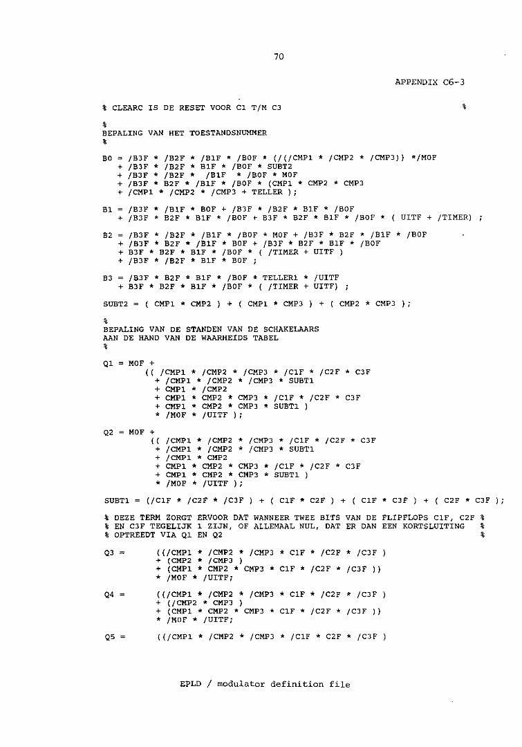
70
APPENDIX C6-3
% CLEARC IS DE RESET VOOR Cl TIM C3
% BEPALING VAN HET TOESTANDSNUMMER %
BO IB3F' IB2F • IBIF • IBOF * (/(/CMPl * ICMP2 * ICMP3» */MOF + IB3F * IB2F • BIF * IBOF * SUBT2 + IB3F • IB2F' IBIF • IBOF • MOF + IB3F • B2F • IBIF • IBOF • (CMPl • CMP2 * CMP3 + ICMPl * ICMP2 * ICMP3 + TELLER );
Bl IB3F * IBlF * BOF + IB3F * IB2F * BIF * IBOF
%
+ IB3F * B2F * BIF * IBOF + B3F * B2F * BlF * IBOF * ( UITF + ITIMER)
B2 IB3F * IB2F * IBlF * IBOF • MOF + IB3F * B2F * IB1F * IBOF + IB3F • B2F • IB1F • BOF + IB3F • B2F • B1F * IBOF + B3F • B2F • B1F • IBOF • ( ITIMER + UITF ) + IB3F • IB2F • BIF * BOF ;
B3 IB3F' B2F • B1F * IBOF • TELLERl • IUITF + B3F * B2F • B1F • IBOF • ( ITIMER + UITF)
SUBT2 = ( CMPl * CMP2 ) + ( CMPl • CMP3 ) + ( CMP2 * CMP3 );
% BEPALING VAN DE STANDEN VAN DE SCHAKELAARS AAN DE HAND VAN DE WAARHEIDS TABEL %
Ql MOF + (( ICMPl • ICMP2 • ICMP3 • IC1F * IC2F • C3F
+ ICMPl • ICMP2 • ICMP3 • SUBTl + CMPl • ICMP2 + CMPl • CMP2 • CMP3 • ICIF • IC2F • C3F + CMPl • CMP2 • CMP3 * SUBTl ) • IMOF * IUITF );
Q2 MOF + (( ICMPl • ICMP2 * ICMP3 * ICIF * IC2F * C3F + ICMPl • ICMP2 * ICMP3 * SUBTl + /CMPl * CMP2 + CMPl • CMP2 • CMP3 • IC1F • IC2F • C3F + CMPl .. CMP2 * CMP3 * SUBTl ) • IMOF • IUITF );
SUBTl = (/C1F • IC2F • IC3F ) + ( C1F • C2F ) + ( C1F * C3F ) + ( C2F * C3F );
% DEZE TERM ZORGT ERVOOR DAT WANNEER TWEE BITS VAN DE FLIPFLOPS C1F, C2F % % EN C3F TEGELIJK 1 ZIJN, OF ALLEMAAL NUL, DAT ER DAN EEN KORTSLUITING % % OPTREEDT VIA Ql EN Q2 %
Q3 = ( (fCMPl • ICMP2 • ICMP3 'ClF • IC2F * IC3F ) + (CMP2 * jeMP3 ) + (CMPl • CMP2 • CMP3 • C1F • IC2F • IC3F » • IMOF • IUITF;
Q4 ((/CMPl • ICMP2 • ICMP3 • C1F • IC2F • IC3F ) + (f CMP2 • CMP3 ) + (CMPl • CMP2 * CMP3 • elF .. IC2F • IC3F » * /MOF .. jUITFi
Q5 ((/CMPl • ICMP2 • ICMP3 • IClF • C2F • IC3F )
EPLD / modulator definition file

71
+ (/CMPl * CMPJ ) + (CMPl * CMP2 * CMPJ * /C1F * C2F * /CJF )) * /MOF * /UITF;
Q6 «(lCMPl * /CMP2 * /CMPJ * /C1F * C2F * /CJF ) + (CMPl * /CMPJ ) + (CMPl * CMP2 * CMPJ * /C1F * C2F * /CJF )) * /MOF * /UITF;
END$
Teller 1.6 1'-5
Teller1 2.7 1'-5
Timer = 3.9 }J.S
TELLER
TELLER1
TIMER
501'-5
EPLD / modulator definition file
APPENDIX C6-4

: . i
I I Li 1 i , , ,
I : 1 1
I .. ' -11
, 1 ,
s~ I J4. : Jatt~S~, w,~, IC,l1P i ct1J, ":,,. 'c.\.o't\l. i I I I I I il' I I : , ,
(\..::.'t\..eo..-t i i-:'r~;O"'P\ *~"'ll.\'51) & ... llO ......... \j;,\J..,i! II' I,' 'i'
I, I 'I I 'I I 1 I I I , ,
, I
~e" -j " ,,-
C 1 f , C'I. 'f ,ei f I ~~..,..: "''''''' I ~ .. ~ ~\'>"''<,,'' 0(" ~ '1.0 \~
r--,'-,l sy 'I I ,I
ty../)--Mf--
I
I
I I I I I I
--. ..lMD-
• i '~
'"" ! • ~ 13
.H
'" ,n "

RLOGAl
o
-20
-40 dB
-.0
-90
HERTZ
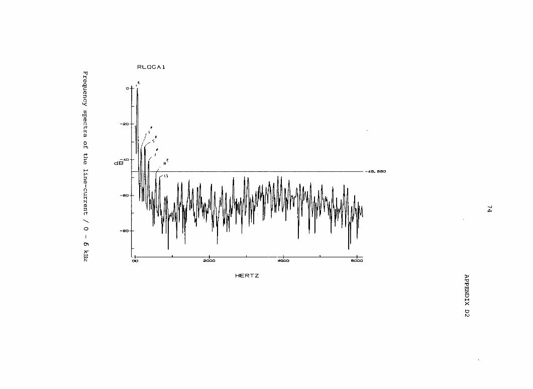
00 '0
'" n rt ~
"' o '" [j.
'" t-' ~.
" '" I n C ~ ~
'" " rt
"o
o
-20-
-40 dB
-eo
-80
RLOGAI
< ,
, ;'
< / ,
I !" ,
" R--f------------------------------------------------------------------------46.e60 1\
00 2000 4000 BOOO
HERTZ
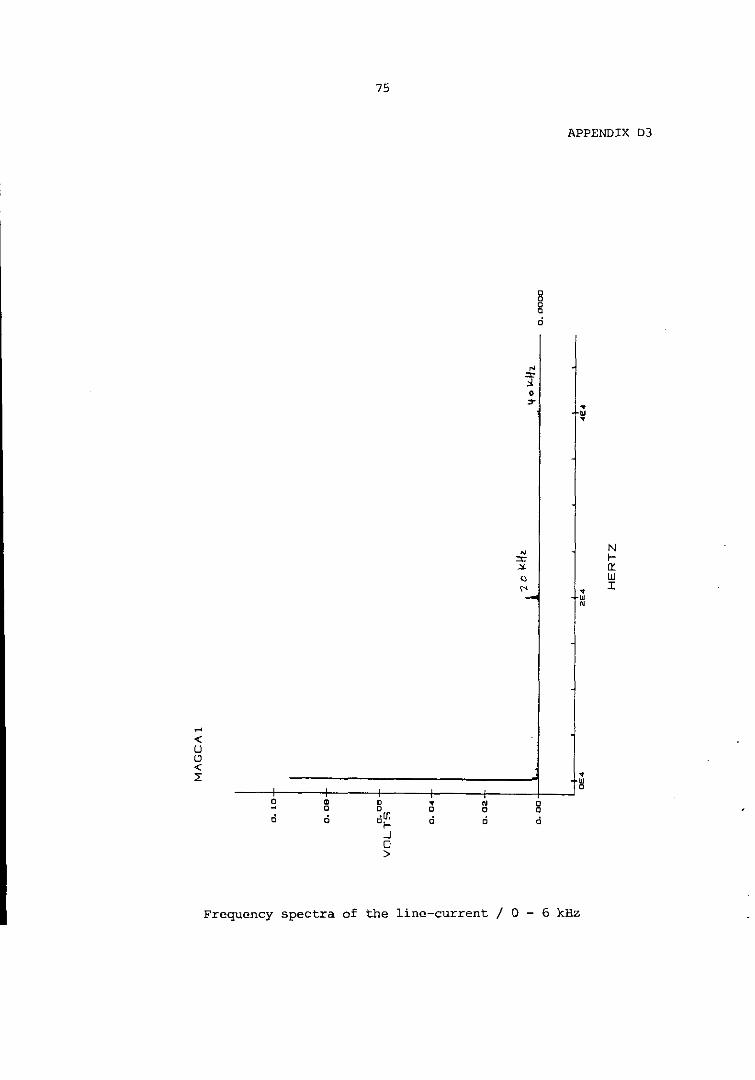
~
< u (.:J
< ~
75
0 • • • 0 0 0
ti .; .1/1 ti of--J 0 >
N 0 0 0
C C
APPENDIX D3
• • •
• • N
• ~ 0
N fIl: w I
Frequency spectra of the line-current I 0 - 6 kHz
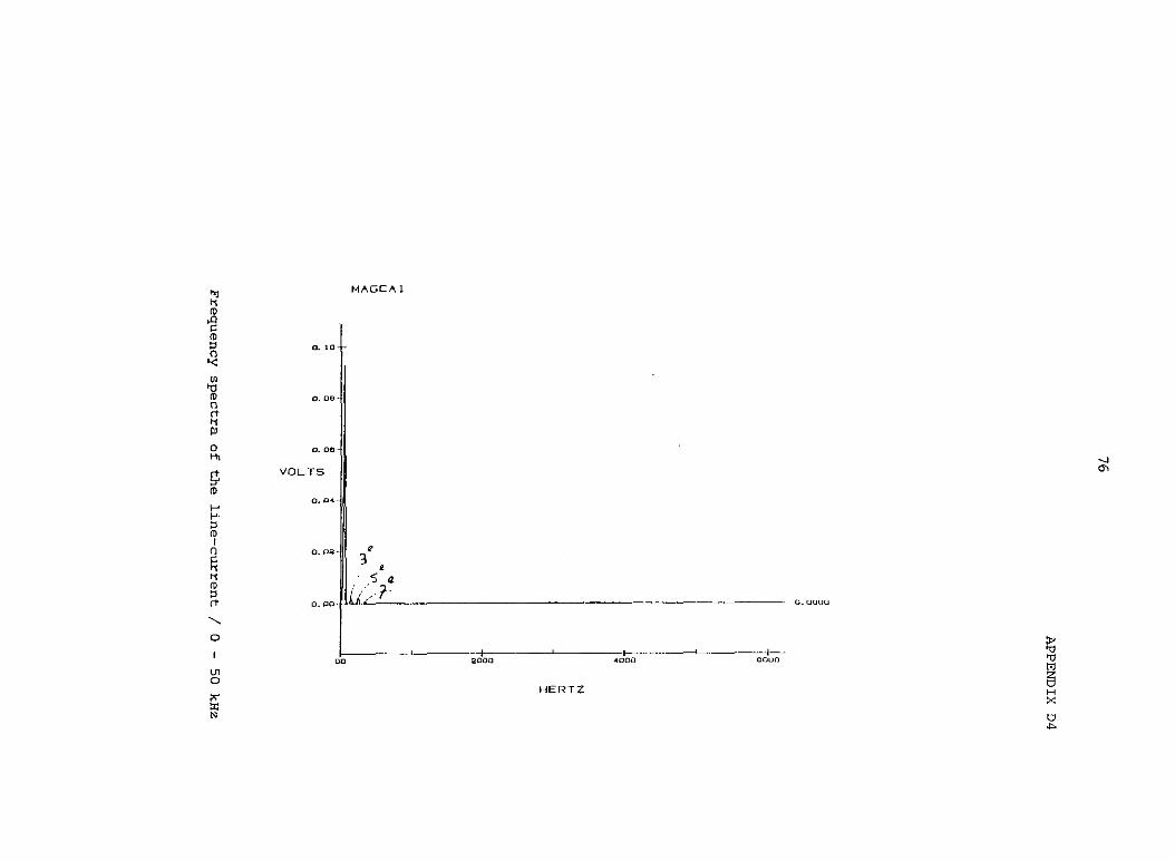
..., MAGC,4,l
" ro .0
" ro :;l n
0.10
'< Ul '0 ro 0.00' n rT Ii PJ 0 c.oe
'" rT VOL TS ~ ro
0.04 >-" ~.
" ro I n o.oa- , " 3 Ii , Ii S a ro J :;l rT 0.00- O.UUllU
"-0
00 .t---------'------~2~Ot~~0------~--------.~O~·------~----- I--eoun
en 0
HERTZ
"" 0:
"
Eindhc:tven Universitv of Tochnoloay Rasearch R%7?rtS
Faculty of Electrical EraineariP9
(223) n?Wiak, L
Tl-E BIT FULL-DECDoFOSITICI'II OF SE(JJENTIAL MtIlO-tlNES. EUT Report 89-E-223. 1989. ISBN 90-6144-223-0
ISSN 0167-9708 COden: TElJEDE
(224) Book of' abstracts of' the first Benelux-Japan WOrkshop on Infonnation and Carn'rLBlication Theory.
Eindhoven. "The Netherlands. 3-5 SeptaytJer 1989. Ed. by Han~. EUT Report B9-E-224. 1989. ISBN 90-6144-224-9
(225) HQei.,.,..ars. M.J.
A POSSIBILITY TO I~TE SAn.RATIC»'II IN "THE SI .......... E. GLCEIAL. M:IJEl... OF A S'VNC:HD'«:US MftICHINE WITIi RECTIFIER.
EUT Report B9-E-225. 1989. ISBN 90-6144-225-7
(226) Dahiva. R.P. and E.M. van Veldhuizen. W.R. LH.Th. RietlanS
EXPERIt-ENTS CI'II INITIAL BEHAVI<1.R OF CCRJNA
BIAS.
BIT Report 89-E-226. 1989. ISBN 90-6144-226-5
WITIi ELECTRICAL PULSES SUPERIMPOSED CI'II DC
(227) Bastiras. R.H.A. ~ THE DEVELOPMENT OF NI INTELLIGENT AI...JIRtot SYSTEM IN ANESTHESIA.
EUT Report B9-E-227. 1989. ISBN 90-6144-227-3
(228) ~. J.J.
c:DoR.JTER ANIP¥l.TED GRAPHICS AS A TEACHIP«:i TOOL. FeR "THE PHESlliESIA f'oN:HlNE SIJIoULA-n:R. BIT Report B9-E-22B. 1989. ISBN 90-6144-228-1
(229) Qostrom. J.H.M. van INTELLIGENT AL..ARMS IN ANESTHESIA: An inpl~tion.
EUT Report B9-E-229. 1989. ISBN 9O-6144-229-X
(Z30) ~. M.R.M. DESIGN OF A ...... 1VERSAl.. PROTtX::Cl.. SLIBSYSTEM ARCHITEcn.RE: Spac:ification of func:tions and services. EUT Report 89-E-230. 19189. ISBN 90-6144-230-3
(231) Schemnann. M.F.C. and H.C. ~. J.J.M. t<»-s?%", Th.G. van de ~
M:l.HTIN:Ii N..:J OC TO 18 GHz OiARACTERISATIDoI OF IXl..Et.E ~IER RESCNANT ~LIN::i DEVICES.
EUT Report B9-E-231. 1989. ISBN 90-6144-231-1
(232) ~, A.D. and M.H.A.J. ~
OATA AC~ISITIDoI AN) SIGtW.. PROCESSING/ANALYSIS OF SCINTILLATIDoI EVENTS FCR THE OLVtoFUS PROPAGATICI'II EXPERIr-ENT.
EUT Report B9-E-232. 1989. ISBN 9O-6144-232-X
(233) Nedarstist. J.A. DESIGN AN) I~EJoENTATIDoI OF A SECCI"IJ PROTOTYPE OF THE INTELLIGENT AI.....ARM SYSTEM IN Al'ES'THESIA.
EUT Report 9O-E-233. 1990. ISBN 90-6144-233-8
(234) pb11iopens. E.H.J.
DESIGNING OEB.JGGING TtXLS FCR SIt-FLEXYS EXPERT SYSTEMS.
ElIT Report 9O-E-234. 1990. ISBN 90-6144-234-6
(235) HaFfelS. J.J.M.
(236)
A PATIENT SIM..A..A-n:R FeR ANESTHESIA "TRAINIPG: A mechanical lW'lg JlDdal and a pt\ysiological sof'twarv nK:dal • ElIT Report 9O-E-235. 1990. ISBN 90-6144-235-4
BASED AI:lI!IPTIVE BI..OCD PRESS..RE CON'TRCI...: A Sinpla><,)l'S expert systan application. ElIT Report 9O-E-236. 1990. ISBN 90-6144-236-2
(237) ~ Qingchang PREDICTIDt ERR(R I'o£1'M:D FeR 10000IFlCATICI'oI OF A HEAT EXO-tAI'IGER. ElIT Report 9O-E-237. 1990. ISBN 90-6144-237-0
(238) L amners, J.O.
THE USE OF PETRI NET "THECRY FCR SIMPLEXYS EXPERT SYSTEMS FROic:x::u.. DECKING. EUT Report 9O-E-23B. 1990. ISBN 90-6144-238-9

Eindhoven university err Technolooy Research WPJrts Faculty err Electrical Engineering
(239)~. X. F'RELIMINOoRY INVESTIGATICHS c:.. TACTILE PERCEPTION OF GRAPHICAL PATTERNS.
a.rr Report 9O-E-239. 1990. ISBN 90-6144-239-7
(240) Lutgens. J.M.A.
I<N:W....ErGE BASE c:aRECTNESS OiECXIr.G FeR SII'4'LEXYS EXPERT SYSTEMS.
BIT Report. 9O-E-24O. 1990. ISBN 90-6144-240-0
(241) Brinker. A.C. den A MEro£RAt£ P-IXlEL FCR SPATI~ COJPLII'G.
a.rr Report 9O-E-241. 1990. ISBN 90-6144-241-9
(242) Kwaspen. J.J.M. and H.C. ~. J.I.M. MICRCWAVE NlISE r-£ASl..REJroEN ON D:UBLE
ElIT Report 9O-E-242. 1990. ISBN 90-6144-242-7
ISSN 0167-9708
COden: TBJEDE
(243) ~. P. and H.A.L-M. de ~. W.J.M. Br'enans. H.G. "" • s. H.H.J. tan ~
F'REDESIGN OF PN EXPERIMENTAL (5-10 r-wt) OISK M-D FPCILITY Pl'£J PROSPECTS OF CO'MERCIAL (1(x)()
~) M-D,/S'TENot SYSTEMS. EUT Rep:lrt 9O-E-243. 1990. ISBN 90-6144-243-5
(244) Klcnpstra. Martin and Ton van den~. Ad ~ A ~ISCl'oI OF CLASSICAL Pl'£J M:IlERN CCNTRCLLER DESIGN: A case stuctY. EUT Report 9O-E-244. 1990. ISBN 90-6144-244-3
(245) ~. P.H.G. van de
a'II -n-tE PCariUlCY OF RADU:IIIt\,VE PROPAGATION f£ASl.REJIoENTS: O1~s ppY."' ........ p·tion experin..-.t.
EUT Report. 9O-E-24S. 1990. ISBN 90-6144-245-1
(246) ~. P.J.I. de
A S"r"N11-tESIS I'£11iCD FeR CQeII'£D OPTIMlZATIai OF ,.,..... TIPLE ANTEJII'IIA PARPfoE"TERS AI'O ~ PATTERN smlJCn.RE.
EUT Report 9O-E-246. 1990. ISBN 9O-6144-246-X
(247) J6Zloliak. L- and T. DEc:GoFOSITICNAL ~CA';;;~ WITH RB.JSE OF STANlARD DESIGNS: Using CClCllters as sub-machines and using the method or maxi ... l ad.jacensies to select the state chains and the state
codas. BUT Report 9O-E-247. 1990. ISBN 90-6144-247-8
(248) Hoei ........ ers. M.J. and J.M. Vleeshc::Ju"ters DERIVATION ND VERIFICATIa'II OF A M:DEL OF "THE SYN:I-RH1JS MQ£H1r£ WITH RECTIFIER WITH "1'l«)
DAf'oFER WINlINGS ON"THE DIRECT AXIS. BUT Report 9O-E-24B. 1990. ISBN 90-6144-248-6
(249) ~. V.C. and A.C.P.M. Backx. P. E'I!4<.hgff
M.A.TIVARI.ABl..E PRCX::ESS IDENTIFICATION FCR ROBUST CCNTROL.
BUT Report 91-E-249. 1991. ISBN 90-6144-249-4
(250) PraffBl2h2fer. F.M. and P.J.M. C1Uitrnan§. H.M. psu1pars EJoIlABS: Design and fonne.l specificat10n ~ a detanDdel fOr a clinical 'l"'Bsee.rch database system. BUT Report 91-E-250. 1991. ISBN 90-6144-250-8
(251) Ei1ndhclvgp. J.T.J. van and G.G. de~. L. ~ "THE ASCIS DATA FLOW GRAPH: SE!mer1tics and textual fonne.t. BUT ~ 91-E-2S1. 1991. ISBN 90-6144-251-6
(252) 0---.. J. and P.J.I. de~. M.H.A.J. ~
WlDE-AtG....E RADIATla'II PATTERN CALaJLATlao. OF PARABOLOIDAL. REFLECTCR .AHTENoIAS: A carparat1va s~.
BUT ~ 91-E-252. 1991. ISBN 90-6144-252-4
(253) ~. S.W.H. de A F"JIM ~-~E INVERTER FeR I~CTION BETWEEN A PHOTCM:Il..TAIC PRRAY N£J THE lITlLITY
LItE. EUT Report 91-E-253. 199],. ISBN 90-6144-253-2