A Presentation on Cascadable Adiabatic Logic Circuits for Low-Power applications By Divya Yashwanth.
37
A Presentation on Cascadable Adiabatic Logic Circuits for Low-Power applications By Divya Yashwanth
-
Upload
abel-pitts -
Category
Documents
-
view
223 -
download
1
Transcript of A Presentation on Cascadable Adiabatic Logic Circuits for Low-Power applications By Divya Yashwanth.
A Presentation on
Cascadable Adiabatic Logic Circuits
for Low-Power applications
By
Divya Yashwanth
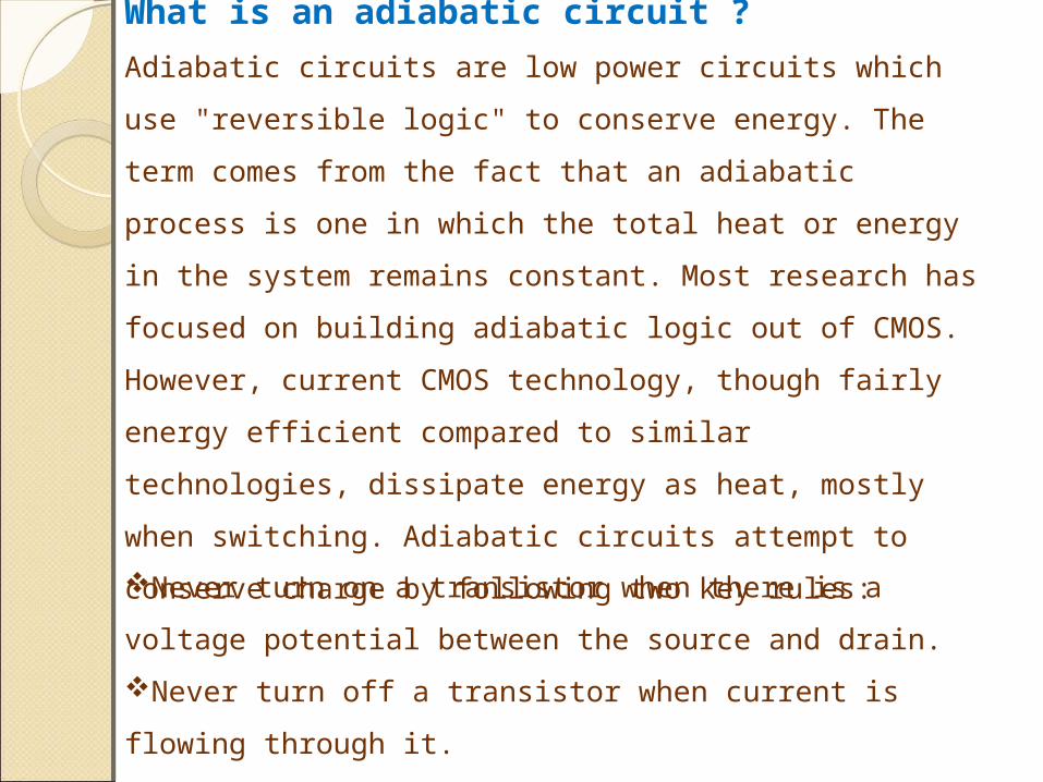
What is an adiabatic circuit ?
Adiabatic circuits are low power circuits which use
"reversible logic" to conserve energy. The term comes
from the fact that an adiabatic process is one in which the
total heat or energy in the system remains constant. Most
research has focused on building adiabatic logic out of
CMOS. However, current CMOS technology, though fairly
energy efficient compared to similar technologies,
dissipate energy as heat, mostly when switching.
Adiabatic circuits attempt to conserve charge by following
two key rules:Never turn on a transistor when there is a voltage
potential between the source and drain.
Never turn off a transistor when current is flowing
through it.
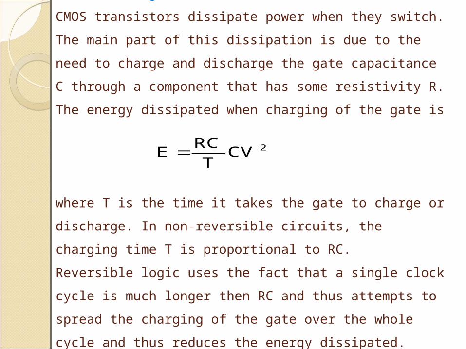
Adiabatic Logic circuits from CMOS
CMOS transistors dissipate power when they switch. The
main part of this dissipation is due to the need to charge
and discharge the gate capacitance C through a component
that has some resistivity R. The energy dissipated when
charging of the gate is
where T is the time it takes the gate to charge or discharge.
In non-reversible circuits, the charging time T is proportional
to RC. Reversible logic uses the fact that a single clock
cycle is much longer then RC and thus attempts to spread
the charging of the gate over the whole cycle and thus
reduces the energy dissipated.
2CVT
RCE
In order to extend the charging time of the gate never turn
on a transistor that has a potential difference between
source and drain, and furthermore, once the transistor is
turned on, energy flows through it in a gradual and
controlled manner.
The second rule that adiabatic circuits must follow is
never to turn off a transistor when there is current flowing
through it because transistors are not perfect switches
going from on to off instantly. Instead, it gradually changes
from on to off when the gate voltage changes.
Furthermore, the change is proportional to the speed at
which the gate voltage changes. During this time, the
voltage drop across the transistor greatly increases yet the
resistance is not high enough to bring power dissipation to
zero.
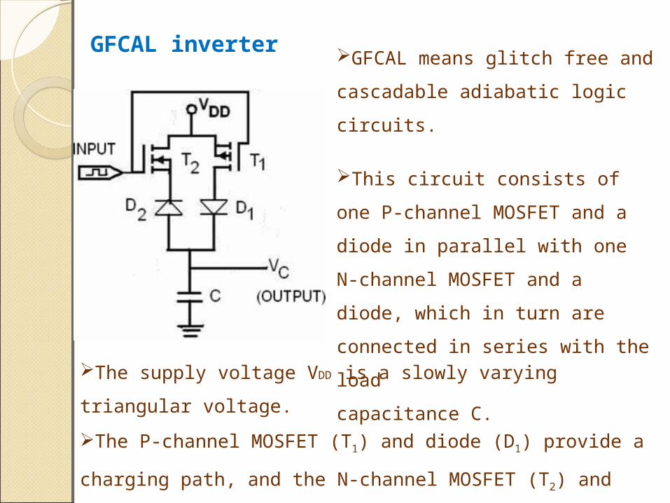
GFCAL inverter GFCAL means glitch free and
cascadable adiabatic logic
circuits.
This circuit consists of one P-
channel MOSFET and a diode in
parallel with one N-channel
MOSFET and a diode, which in
turn are connected in series with
the load
capacitance C.The supply voltage VDD is a slowly varying triangular
voltage.
The P-channel MOSFET (T1) and diode (D1) provide a
charging path, and the N-channel MOSFET (T2) and diode
(D2) provide a discharging path for the load current.
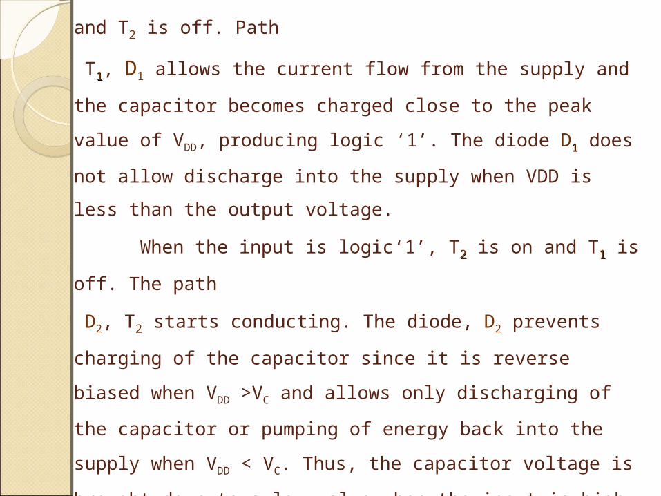
Operation of the circuit
When the input is ‘0’ (logic ‘0’), T11 is on and T2 is off.
Path
T11, D1 allows the current flow from the supply and the
capacitor becomes charged close to the peak value of VDD,
producing logic ‘1’. The diode D11 does not allow discharge
into the supply when VDD is less than the output voltage.
When the input is logic‘1’, T22 is on and T11 is off. The
path
D2, T2 starts conducting. The diode, D2 prevents charging of
the capacitor since it is reverse biased when VDD >VC and
allows only discharging of the capacitor or pumping of
energy back into the supply when VDD < VC. Thus, the
capacitor voltage is brought down to a low value when the
input is high irrespective of the previous output. Hence, the
output is the complement of the input.
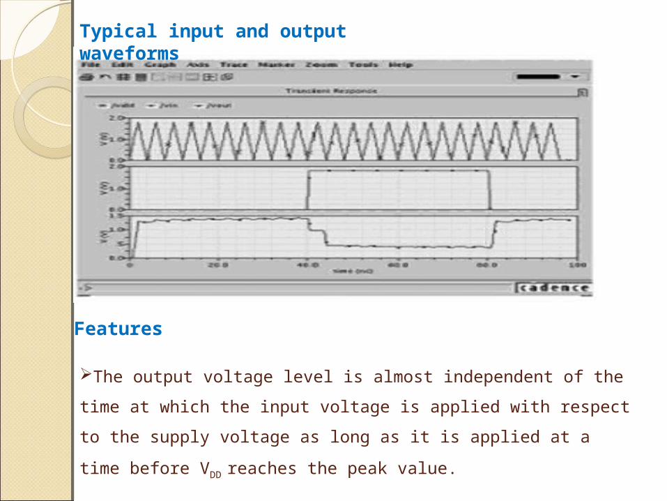
The output voltage level is almost independent of the time at
which the input voltage is applied with respect to the supply
voltage as long as it is applied at a time before VDD reaches the
peak value.
Features
Typical input and output waveforms
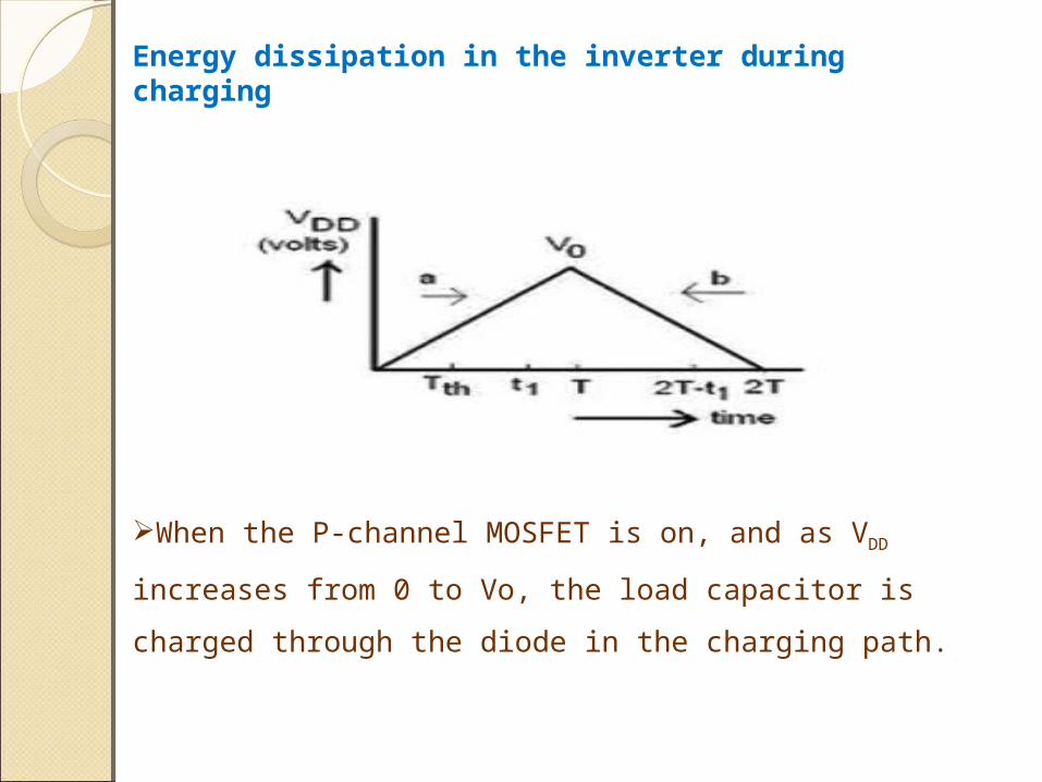
Energy dissipation in the inverter during charging
When the P-channel MOSFET is on, and as VDD
increases from 0 to Vo, the load capacitor is charged
through the diode in the charging path.
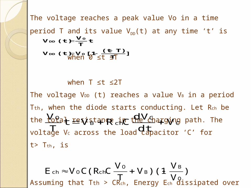
The voltage reaches a peak value Vo in a time period T and
its value VDD(t) at any time ‘t’ is
when 0 ≤t ≤T
when T ≤t ≤2T
The voltage VDD (t) reaches a value VB in a period Tth, when
the diode starts conducting. Let Rch be the total resistance in
the charging path. The voltage VC across the load capacitor
‘C’ for
t> Tth, is
Assuming that Tth > CRch, Energy Ech dissipated over the
period
0 – T in the diode and the transistor is
]TT)(t
[1V(t)V
tTV
(t)V
ODD
ODD
CC
chBO
Vdt
dVCRVt
TV
)VV
)(1VTV
CC(RVEO
BB
OchOch
Energy dissipation in the inverter during discharging
When the N-channel MOSFET is on, the P-channel MOSFET
is off, charging of the capacitor is prevented at the load and the
capacitor discharges through the diode in the discharge path till t1,
that is, till VC is higher than the supply by at least VB, during the
period when VDD increases from 0 to Vo. The capacitor then stops
discharging at t1 and again continues discharging from 2T–t1 until
VC = VB. Let Rdis be the total resistance in the discharging path.
Assuming CRdis < t1, the energy Edc dissipated during discharging is
the sum of energy dissipated during 0 to t1 and (2T–t1 ) to 2T which
can be shown to be
where
C2
B2BCVBCR
TV
2C-)RC2TV(2tE Bdis
Odis
2O
2
1dc
TV
CRVVBO
disBCO
The total energy ED, dissipated during one cycle of charging
and discharging is given by
C2BBCVBCR
TV
2C)RCTV(2t)
VV
)(1VTV
CC(RVEEE2
BdisO
dis2
2
2O
1O
BB
OchOdcchD
Where t1 is given by
}
TC
RV
)TC
R(VVVCln{Rt
disO
disOBCO
dis1
Equation (1)
From equation (1)the energy dissipated decreases as T
increases. T indicates the rate at which the supply voltage
varies and, hence, the energy dissipated decreases with
slowly varying the supply voltages. The power dissipation
generally changes with parameters like VO, the value of the
capacitance, the equivalent series resistance because of
the diode and the MOSFET.
Simulation of the inverter
Simulated using Virtuoso Spectre circuit simulator of
Cadence EDA tools.
Models used for the simulation are BSIM3V3 model
parameters.
Length of the transistor=180nm, width of the transistor =
720nm.
Load capacitance=30fF.
Supply waveform is triangular with frequency=25MHz and
peak supply voltage=1.8V.
Input signal is square wave with frequency=25MHz.
The input logic ‘0’ value is 0.45 V and input logic ‘1’ value is
1.4 V.
The output logic values have been found to be 0.45
and 1.4 V corresponding to logic ‘0’ and logic ‘1’,
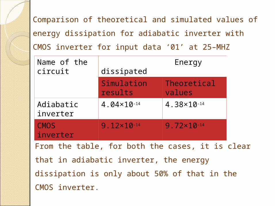
Name of the circuit
Energy dissipated
Simulation results
Theoretical values
Adiabatic inverter
4.04×10⁻¹⁴ 4.38×10⁻¹⁴
CMOS inverter 9.12×10⁻¹⁴ 9.72×10⁻¹⁴
Comparison of theoretical and simulated values of energy
dissipation for adiabatic inverter with CMOS inverter for
input data ‘01’ at 25–MHZ
From the table, for both the cases, it is clear that in
adiabatic inverter, the energy dissipation is only about
50% of that in the CMOS inverter.
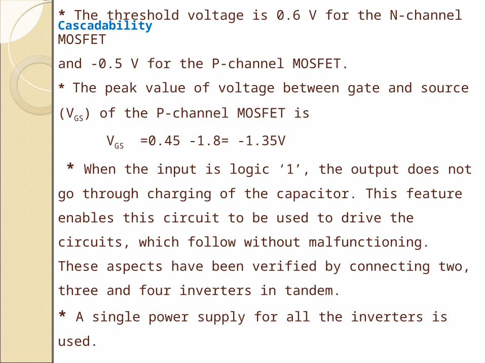
* The threshold voltage is 0.6 V for the N-channel MOSFET
and -0.5 V for the P-channel MOSFET.
* The peak value of voltage between gate and source (VGS) of
the P-channel MOSFET is
VGS =0.45 -1.8= -1.35V
* When the input is logic ‘1’, the output does not go
through charging of the capacitor. This feature enables this
circuit to be used to drive the circuits, which follow without
malfunctioning. These aspects have been verified by
connecting two, three and four inverters in tandem.
* A single power supply for all the inverters is used.
Cascadability
Effect of variation of frequency
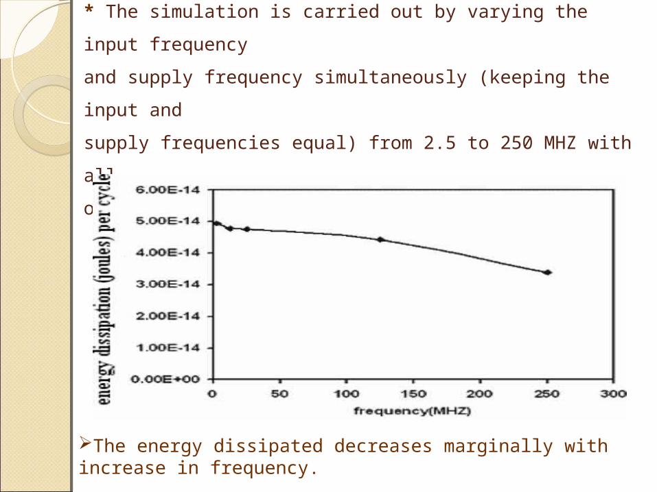
* The simulation is carried out by varying the input
frequency
and supply frequency simultaneously (keeping the input
and
supply frequencies equal) from 2.5 to 250 MHZ with all
other circuit parameters remaining the same.
The energy dissipated decreases marginally with increase in frequency.
The output logic levels up to frequencies of 25 MHz are 1.4
V
corresponding to logic ‘1’ and 0.45 V corresponding to logic
‘0’.
At frequencies higher than 25 MHz, the energy dissipated
decreases gradually and the logic values vary from 1.4 to
1.35 V for logic ‘1’ and 0.45 to 0.47 V for logic ‘0’ at 250
MHz
At frequencies of 2.50 GHz, the logic ‘1’ tends to a value
of 0.8 V and logic ‘0’ of –0.6 V. This is because the time
period of the supply waveform is small compared with the
time constant of charging and discharging, and the
capacitor is unable to charge and discharge to the required
levels.
The frequency of operation is increased by increasing the
width of the transistors, which results in a decrease of the
charging and discharging time constants but large W/L ratio
results in higher power dissipation in both the CMOS and
GFCAL circuits.
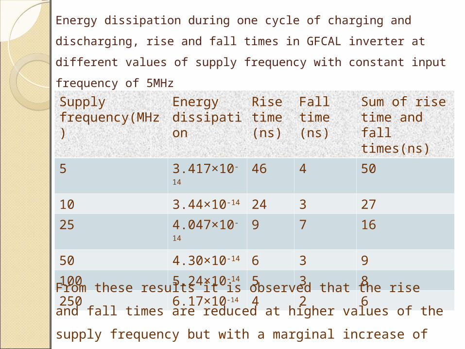
Energy dissipation during one cycle of charging and discharging,
rise and fall times in GFCAL inverter at different values of supply
frequency with constant input frequency of 5MHz
Supply frequency(MHz)
Energy dissipation
Rise time (ns)
Fall time (ns)
Sum of rise time and fall times(ns)
5 3.417×10-
14
46 4 50
10 3.44×10⁻¹⁴ 24 3 27
25 4.047×10-
14
9 7 16
50 4.30×10⁻¹⁴ 6 3 9
100 5.24×10⁻¹⁴ 5 3 8
250 6.17×10⁻¹⁴ 4 2 6From these results it is observed that the rise and fall times
are reduced at higher values of the supply frequency but
with a marginal increase of energy dissipation.
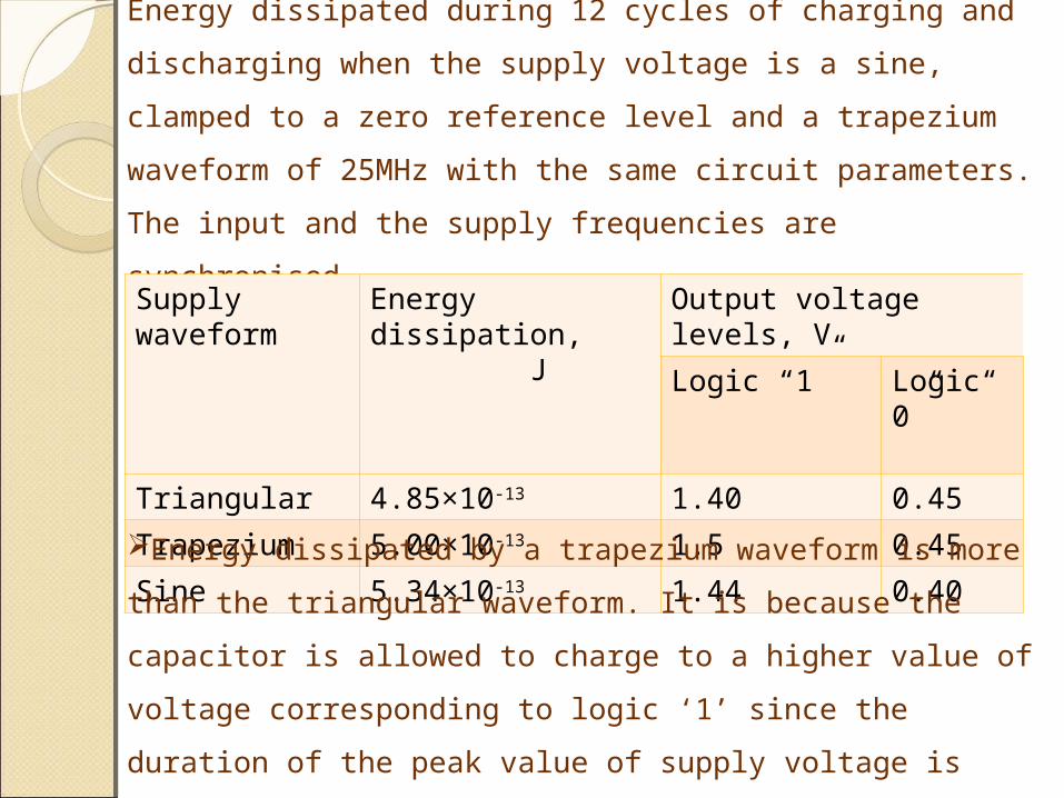
Energy dissipated during 12 cycles of charging and
discharging when the supply voltage is a sine, clamped to a
zero reference level and a trapezium waveform of 25MHz
with the same circuit parameters. The input and the supply
frequencies are synchronised.
Supply waveform
Energy dissipation, J
Output voltage levels, V
Logic “1” Logic“0”
Triangular 4.85×10⁻¹³ 1.40 0.45
Trapezium 5.00×10⁻¹³ 1.5 0.45
Sine 5.34×10⁻¹³ 1.44 0.40
Energy dissipated by a trapezium waveform is more than
the triangular waveform. It is because the capacitor is
allowed to charge to a higher value of voltage corresponding
to logic ‘1’ since the duration of the peak value of supply
voltage is longer compared with that of the triangular wave
form.
In the case of the sine wave, the energy dissipation is
more than that in the above cases because of the fast
voltage rise near the zero crossing. Therefore triangular
waveform is more suitable for less energy dissipation.
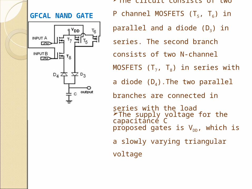
The circuit consists of two P
channel MOSFETS (T5, T6) in parallel
and a diode (D3) in series. The
second branch consists of two N-
channel MOSFETS (T7, T8) in series
with a diode (D4).The two parallel
branches are connected in series
with the load capacitance C
GFCAL NAND GATE
The supply voltage for the
proposed gates is VDD, which is a
slowly varying triangular voltage
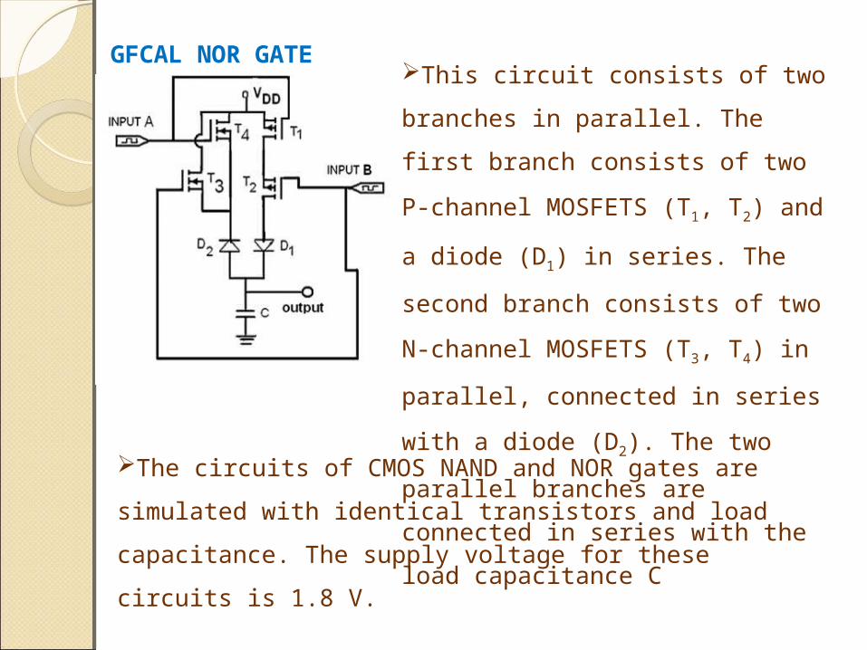
GFCAL NOR GATEThis circuit consists of two
branches in parallel. The first
branch consists of two P-channel
MOSFETS (T1, T2) and a diode (D1) in
series. The second branch consists
of two N-channel MOSFETS (T3, T4)
in parallel, connected in series with
a diode (D2). The two parallel
branches are connected in series
with the load capacitance CThe circuits of CMOS NAND and NOR gates are
simulated with identical transistors and load capacitance.
The supply voltage for these circuits is 1.8 V.
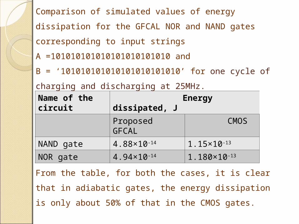
Comparison of simulated values of energy dissipation for the
GFCAL NOR and NAND gates corresponding to input strings
A =101010101010101010101010 and
B = ‘101010101010101010101010’ for one cycle of
charging and discharging at 25MHz.
Name of the circuit
Energy dissipated, J
Proposed GFCAL CMOS
NAND gate 4.88×10⁻¹⁴ 1.15×10⁻¹³
NOR gate 4.94×10⁻¹⁴ 1.180×10⁻¹³
From the table, for both the cases, it is clear that in
adiabatic gates, the energy dissipation is only about 50%
of that in the CMOS gates.
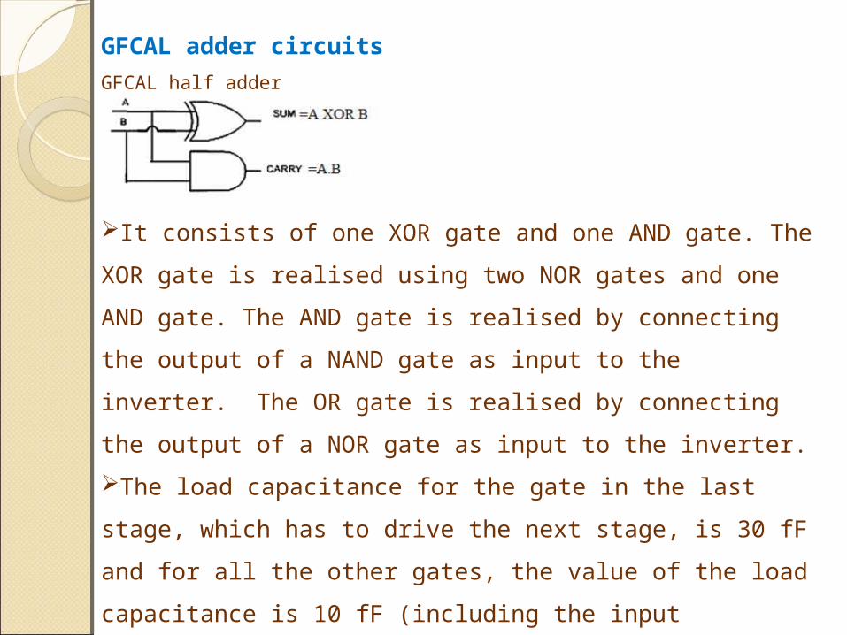
GFCAL adder circuits
GFCAL half adder
It consists of one XOR gate and one AND gate. The XOR
gate is realised using two NOR gates and one AND gate. The
AND gate is realised by connecting the output of a NAND
gate as input to the inverter. The OR gate is realised by
connecting the output of a NOR gate as input to the
inverter.
The load capacitance for the gate in the last stage, which
has to drive the next stage, is 30 fF and for all the other
gates, the value of the load capacitance is 10 fF (including
the input capacitance of the next stage). The supply for all
the circuits is a triangular waveform
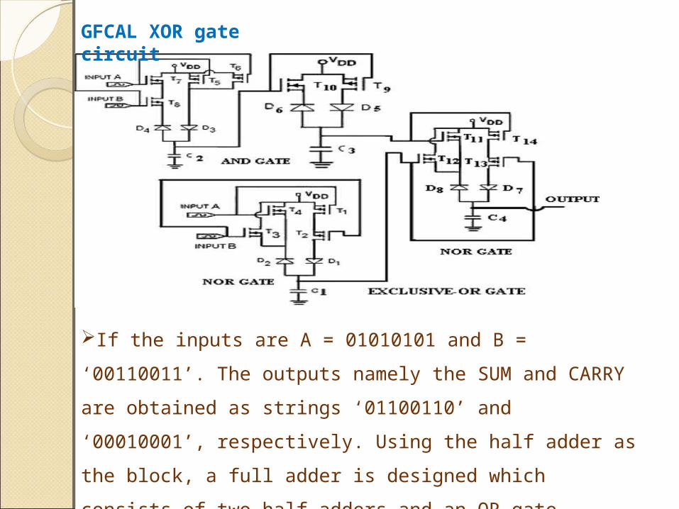
GFCAL XOR gate circuit
If the inputs are A = 01010101 and B = ‘00110011’. The
outputs namely the SUM and CARRY are obtained as
strings ‘01100110’ and ‘00010001’, respectively. Using the
half adder as the block, a full adder is designed which
consists of two half adders and an OR gate.
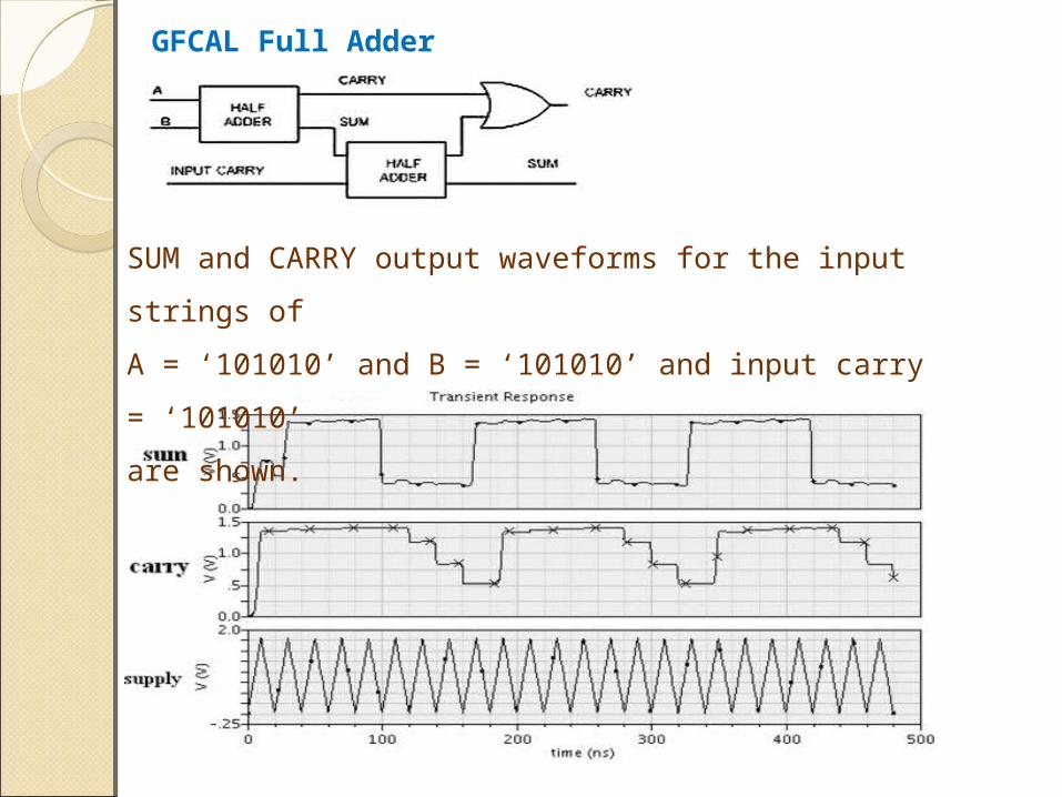
GFCAL Full Adder
SUM and CARRY output waveforms for the input
strings of
A = ‘101010’ and B = ‘101010’ and input carry =
‘101010’
are shown.
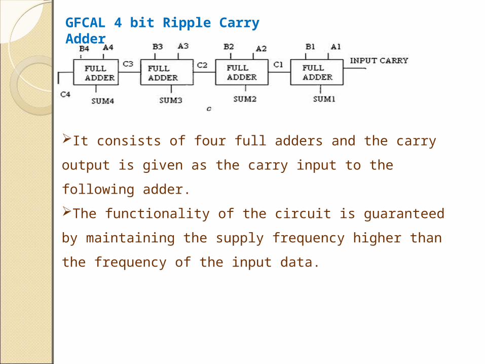
GFCAL 4 bit Ripple Carry Adder
It consists of four full adders and the carry output is
given as the carry input to the following adder.
The functionality of the circuit is guaranteed by
maintaining the supply frequency higher than the
frequency of the input data.
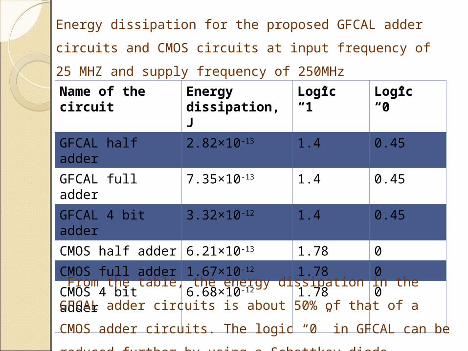
Energy dissipation for the proposed GFCAL adder circuits
and CMOS circuits at input frequency of 25 MHZ and
supply frequency of 250MHz
Name of the circuit
Energy dissipation, J
Logic “1”
Logic “0”
GFCAL half adder 2.82×10⁻¹³ 1.4 0.45
GFCAL full adder 7.35×10⁻¹³ 1.4 0.45
GFCAL 4 bit adder
3.32×10⁻¹² 1.4 0.45
CMOS half adder 6.21×10⁻¹³ 1.78 0
CMOS full adder 1.67×10⁻¹² 1.78 0
CMOS 4 bit adder 6.68×10⁻¹² 1.78 0
From the table, the energy dissipation in the GFCAL adder
circuits is about 50% of that of a CMOS adder circuits. The
logic “0” in GFCAL can be reduced further by using a
Schottkey diode
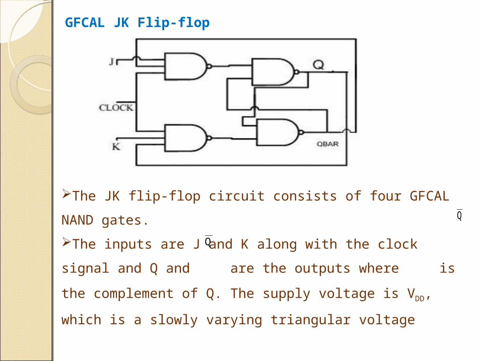
GFCAL JK Flip-flop
The JK flip-flop circuit consists of four GFCAL NAND gates.
The inputs are J and K along with the clock signal and Q
and are the outputs where is the complement of Q.
The supply voltage is VDD, which is a slowly varying
triangular voltage
Q
Q
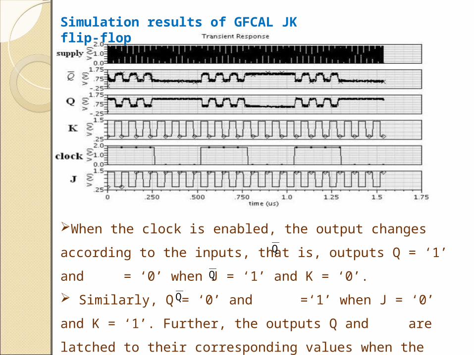
Simulation results of GFCAL JK flip-flop
When the clock is enabled, the output changes according
to the inputs, that is, outputs Q = ‘1’ and = ‘0’ when J =
‘1’ and K = ‘0’.
Similarly, Q = ‘0’ and =‘1’ when J = ‘0’ and K = ‘1’.
Further, the outputs Q and are latched to their
corresponding values when the clock input is disabled.
Q
Q
Q
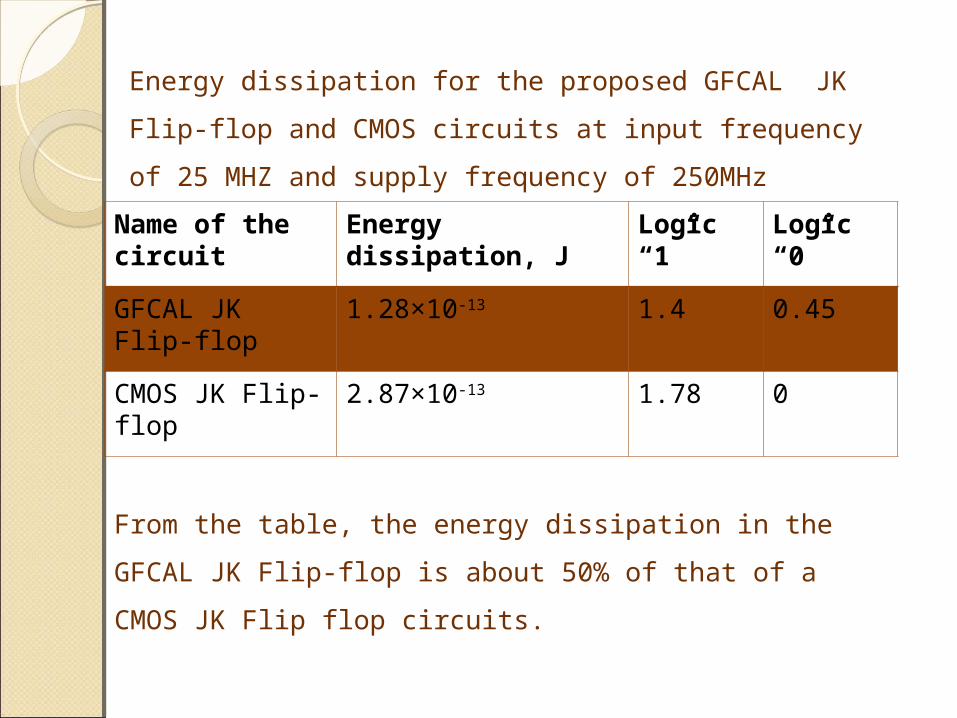
Energy dissipation for the proposed GFCAL JK Flip-flop
and CMOS circuits at input frequency of 25 MHZ and
supply frequency of 250MHz
Name of the circuit
Energy dissipation, J
Logic “1”
Logic “0”
GFCAL JK Flip-flop
1.28×10⁻¹³ 1.4 0.45
CMOS JK Flip-flop
2.87×10⁻¹³ 1.78 0
From the table, the energy dissipation in the GFCAL JK
Flip-flop is about 50% of that of a CMOS JK Flip flop
circuits.
Comparison of proposed GFCAL family with other adiabatic logic families
Given the length and width of a transistor are 180 nm and
720 nm, respectively, and the value of load capacitance is
30 fF. The input frequency is same as the supply frequency
(25 MHZ).
A 2N-2N2D inverter uses four transistors and two-diodes.
The capacitor has to be charged first before evaluating the
outputs, which may cause unwanted switching activities at
the output nodes.
A 2N-2P inverter uses four-transistors and a 2N-2N2P
inverter uses six-transistors. A PAL inverter uses four-
transistors but requires two complementary sinusoidal
power clocks in cascaded circuits.
* A CAL inverter contains eight-transistors and needs a single clock
and two additional timing control clocks for correct operation.
* A True single phase energy recovery logic (TSEL) inverter
contains six-transistors and needs a single clock, but it has
discharge /charge and evaluation phases, which may cause
unnecessary switching activities at nodes in hierarchical
circuits.
* A Quasi-static energy recovery logic (QSERL) inverter
contains four transistors and needs a single clock, but a
threshold voltage drop at MOSFETS used as diodes will
occur and also the capacitance effect exists at higher
frequencies.
* An ADL inverter contains one-transistor and one diode
along with a load capacitor and needs a four-phase clock in
cascaded circuits. Since the capacitor has to be pre-
charged, unwanted switching activity may occur at the
output nodes.
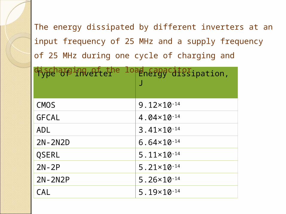
Type of inverter Energy dissipation, J
CMOS 9.12×10⁻¹⁴
GFCAL 4.04×10⁻¹⁴
ADL 3.41×10⁻¹⁴
2N-2N2D 6.64×10⁻¹⁴
QSERL 5.11×10⁻¹⁴
2N-2P 5.21×10⁻¹⁴
2N-2N2P 5.26×10⁻¹⁴
CAL 5.19×10⁻¹⁴
The energy dissipated by different inverters at an input
frequency of 25 MHz and a supply frequency of 25 MHz
during one cycle of charging and discharging of the load
capacitor
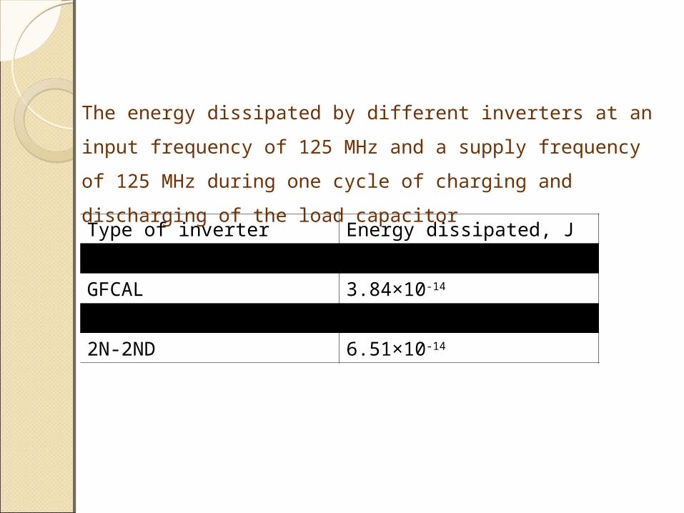
Type of inverter Energy dissipated, J
CMOS 9.15×10⁻¹⁴
GFCAL 3.84×10⁻¹⁴
ADL 3.64×10⁻¹⁴
2N-2ND 6.51×10⁻¹⁴
The energy dissipated by different inverters at an input
frequency of 125 MHz and a supply frequency of 125 MHz
during one cycle of charging and discharging of the load
capacitor
CONCLUSIONS
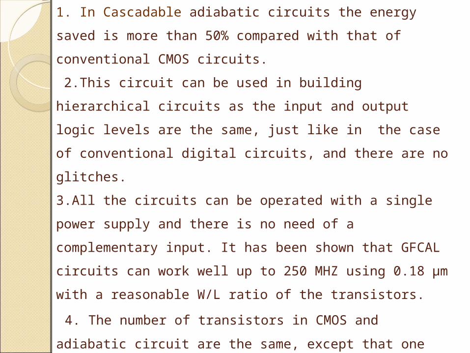
1. In Cascadable adiabatic circuits the energy saved is more
than 50% compared with that of conventional CMOS
circuits.
2.This circuit can be used in building hierarchical circuits as
the input and output logic levels are the same, just like in
the case of conventional digital circuits, and there are no
glitches.
3.All the circuits can be operated with a single power supply
and there is no need of a complementary input. It has been
shown that GFCAL circuits can work well up to 250 MHZ
using 0.18 μm with a reasonable W/L ratio of the transistors.
4. The number of transistors in CMOS and adiabatic circuit
are the same, except that one diode per branch is extra in
adiabatic circuit. Thus, the circuits can be easily cascaded.
5. Power saving in these circuits is because of
(i) The supply voltage is a slowly varying voltage, which
results in energy saving during charging and discharging.
(ii) The energy stored in the load capacitor is pumped back
into the supply to realise a transition from logic ‘1’ to logic
‘0’.
(iii) There is no short circuit current from the supply to the
ground at any time during the transition of logic ‘1’ to logic
‘0’ or logic ‘0’ to logic ‘1’ unlike in the CMOS circuits.
(iv) The diode in the discharge path of the gate prevents the
flow of current spikes from the input data into the load
capacitor.
REFERENCES
1. Cascadable adiabatic logic circuits for low-power
applications
N.S.S. Reddy, M. Satyam, K.L. Kishore, IET Circuits,
Devices and Systems November 2008, Volume 2, No.6,
Pages 518-526.
2. Adiabatic Logic by Benjamin Gojman, August 8, 2004
http://www.cs.caltech.edu/cbsss/finalreport/nanoscale_ind_g
ojman.pdf
3. ‘Second-order adiabatic computation with 2N-2P and 2N-
2N-2P logic circuits’ by Kramer A, Denker J.S., Flower B,
Moroney J, Proc. Intern. Symposium on Low Power Design,
1995, pp.191–196