
A photonic analog-to-digital converter based on an unbalanced Mach-Zehnder quantizer
6
A photonic analog-to-digital converter based on an unbalanced Mach-Zehnder quantizer Chris H. Sarantos and Nadir Dagli* Department of Electrical Engineering, University of California Santa Barbara, CA, 93106, USA *[email protected] Abstract: A Mach-Zehnder modulator (MZM) based analog to digital converter (ADC) is described. The signal to be digitized is applied to a single electrode of a high speed unbalanced modulator that acts as a quantizer. The rest of the system consists of commercially available wavelength division multiplexing (WDM) components. Analysis indicates that 6 bit operation at 40 Giga Samples per second (GS/s) is possible with moderate optical carrier power. ©2010 Optical Society of America OCIS codes: (130.0130) Integrated optics; (130.3120 Integrated optics devices; (230.4110) Modulators; (060.2330) Fiber optics communications. References and links 1. F. Coppinger, A. Bhushan, and B. Jalali, “Photonic time stretch and its application to analog-to-digital conversion,” IEEE Trans. Microw. Theory Tech. 47(7), 1309–1314 (1999). 2. C. Xu, and X. Liu, “Photonic analog-to-digital converter using soliton self-frequency shift and interleaving spectral filters,” Opt. Lett. 28(12), 986–988 (2003). 3. S. Oda, and A. Maruta, “A Novel Quantization Scheme by Slicing Supercontinuum Spectrum for All-Optical Analog-to-Digital Conversion,” IEEE Photon. Technol. Lett. 17(2), 465–467 (2005). 4. T. Nishitani, T. Konishi, and K. Itoh, “Resolution Improvement of All-Optical Analog-to-Digital Conversion Employing Self-frequency Shift and Self-Phase-Modulation-Induced Spectral Compression,” IEEE J. Sel. Top. Quantum Electron. 14(3), 724–732 (2008). 5. R. Pant, C. Xiong, S. Madden, B. L. Davies, and B. J. Eggleton, “Investigation of all-optical analog-to-digital quantization using a chalcogenide waveguide: A step towards on-chip analog-to-digital conversion,” Opt. Commun. 283(10), 2258–2262 (2010). 6. Y. Miyoshi, S. Takagi, S. Namiki, and K. Kitayama, “Multiperiod PM-NOLM With Dynamic Counter- Propagating Effects Compensation for 5-Bit All-Optical Analog-to-Digital Conversion and Its Performance Evaluations,” J. Lightwave Technol. 28(4), 415–422 (2010). 7. B. Shoop, Photonic analog-to-digital conversion, (Springer-Verlag, 2001). 8. C. Sarantos and N. Dagli, “An Unbalanced MZM based Photonic Analog-to-Digital Converter,” Proceedings of IEEE/LEOS 2007 Annual Meeting, pp. 110-111, 2007. 9. Q. Wu, H. Zhang, Y. Peng, X. Fu, and M. Yao, “40GS/s Optical analog-to-digital conversion system and its improvement,” Opt. Express 17(11), 9252–9257 (2009). 10. E. A. J. Marcatili, “Optical subpicosecond gate,” Appl. Opt. 19(9), 1468–1476 (1980). 11. J. J. Veselka, and S. K. Korotky, “Pulse Generation for Soliton Systems Using Lithium Niobate Modulators,” IEEE J. Sel. Top. Quantum Electron. 2(2), 300–310 (1996). 12. H. A. Haus, S. T. Kirsch, K. Mathyssek, and F. J. Leonberger, “Picosecond optical sampling,” IEEE J. Quantum Electron. 16(8), 870–874 (1980). 13. D. J. Bachmann, N. Dagli, J. Calusdian, P. E. Pace, and J. P. Powers, Optical Pulse Train Generation Using Modulator Cascades,” Proceedings of IEEE/LEOS 2008 Annual Meeting, Paper TuF-4, pp. 190–191, Newport Beach, CA, November 9–13, 2008. 14. N. Dagli, “Wide Bandwidth Lasers and Modulators for RF Photonics,” IEEE Trans. Microw. Theory Tech. 47(7), 1151–1171 (1999). 15. K. M. Noguchi, and H. Miyazawa, “Design of Ultra Broad Band LiNbO3 Optical Modulators with Ridge Structure,” IEEE Trans. Microw. Theory Tech. MTT-43, 2203–2207 (1995). 16. J. H. Shin, S. Wu, and N. Dagli, “35 GHz Bandwidth, 5 V-cm Drive Voltage, Bulk GaAs Substrate Removed Electro Optic Modulators,” IEEE Photon. Technol. Lett. 19(18), 1362–1364 (2007). 17. Y. Miyamoto, M. Yoneyama, Y. Imai, K. Kato, and H. Tsunetsugu, “40 Gbit/s optical receiver module using a flip-chip bonding technique for device interconnection,” Electron. Lett. 34(5), 493–494 (1998). 18. G. Agrawal, Fiber Optic Communications Systems, Section 4.6.1, (Wiley, 1997). #127263 - $15.00 USD Received 20 Apr 2010; revised 2 Jun 2010; accepted 21 Jun 2010; published 23 Jun 2010 (C) 2010 OSA 5 July 2010 / Vol. 18, No. 14 / OPTICS EXPRESS 14598
Transcript of A photonic analog-to-digital converter based on an unbalanced Mach-Zehnder quantizer

A photonic analog-to-digital converter based on an unbalanced Mach-Zehnder quantizer
Chris H. Sarantos and Nadir Dagli*
Department of Electrical Engineering, University of California Santa Barbara, CA, 93106, USA *[email protected]
Abstract: A Mach-Zehnder modulator (MZM) based analog to digital converter (ADC) is described. The signal to be digitized is applied to a single electrode of a high speed unbalanced modulator that acts as a quantizer. The rest of the system consists of commercially available wavelength division multiplexing (WDM) components. Analysis indicates that 6 bit operation at 40 Giga Samples per second (GS/s) is possible with moderate optical carrier power.
©2010 Optical Society of America
OCIS codes: (130.0130) Integrated optics; (130.3120 Integrated optics devices; (230.4110) Modulators; (060.2330) Fiber optics communications.
References and links
1. F. Coppinger, A. Bhushan, and B. Jalali, “Photonic time stretch and its application to analog-to-digital conversion,” IEEE Trans. Microw. Theory Tech. 47(7), 1309–1314 (1999).
2. C. Xu, and X. Liu, “Photonic analog-to-digital converter using soliton self-frequency shift and interleaving spectral filters,” Opt. Lett. 28(12), 986–988 (2003).
3. S. Oda, and A. Maruta, “A Novel Quantization Scheme by Slicing Supercontinuum Spectrum for All-Optical Analog-to-Digital Conversion,” IEEE Photon. Technol. Lett. 17(2), 465–467 (2005).
4. T. Nishitani, T. Konishi, and K. Itoh, “Resolution Improvement of All-Optical Analog-to-Digital Conversion Employing Self-frequency Shift and Self-Phase-Modulation-Induced Spectral Compression,” IEEE J. Sel. Top. Quantum Electron. 14(3), 724–732 (2008).
5. R. Pant, C. Xiong, S. Madden, B. L. Davies, and B. J. Eggleton, “Investigation of all-optical analog-to-digital quantization using a chalcogenide waveguide: A step towards on-chip analog-to-digital conversion,” Opt. Commun. 283(10), 2258–2262 (2010).
6. Y. Miyoshi, S. Takagi, S. Namiki, and K. Kitayama, “Multiperiod PM-NOLM With Dynamic Counter-Propagating Effects Compensation for 5-Bit All-Optical Analog-to-Digital Conversion and Its Performance Evaluations,” J. Lightwave Technol. 28(4), 415–422 (2010).
7. B. Shoop, Photonic analog-to-digital conversion, (Springer-Verlag, 2001). 8. C. Sarantos and N. Dagli, “An Unbalanced MZM based Photonic Analog-to-Digital Converter,” Proceedings of
IEEE/LEOS 2007 Annual Meeting, pp. 110-111, 2007. 9. Q. Wu, H. Zhang, Y. Peng, X. Fu, and M. Yao, “40GS/s Optical analog-to-digital conversion system and its
improvement,” Opt. Express 17(11), 9252–9257 (2009). 10. E. A. J. Marcatili, “Optical subpicosecond gate,” Appl. Opt. 19(9), 1468–1476 (1980). 11. J. J. Veselka, and S. K. Korotky, “Pulse Generation for Soliton Systems Using Lithium Niobate Modulators,”
IEEE J. Sel. Top. Quantum Electron. 2(2), 300–310 (1996). 12. H. A. Haus, S. T. Kirsch, K. Mathyssek, and F. J. Leonberger, “Picosecond optical sampling,” IEEE J. Quantum
Electron. 16(8), 870–874 (1980). 13. D. J. Bachmann, N. Dagli, J. Calusdian, P. E. Pace, and J. P. Powers, Optical Pulse Train Generation Using
Modulator Cascades,” Proceedings of IEEE/LEOS 2008 Annual Meeting, Paper TuF-4, pp. 190–191, Newport Beach, CA, November 9–13, 2008.
14. N. Dagli, “Wide Bandwidth Lasers and Modulators for RF Photonics,” IEEE Trans. Microw. Theory Tech. 47(7), 1151–1171 (1999).
15. K. M. Noguchi, and H. Miyazawa, “Design of Ultra Broad Band LiNbO3 Optical Modulators with Ridge Structure,” IEEE Trans. Microw. Theory Tech. MTT-43, 2203–2207 (1995).
16. J. H. Shin, S. Wu, and N. Dagli, “35 GHz Bandwidth, 5 V-cm Drive Voltage, Bulk GaAs Substrate Removed Electro Optic Modulators,” IEEE Photon. Technol. Lett. 19(18), 1362–1364 (2007).
17. Y. Miyamoto, M. Yoneyama, Y. Imai, K. Kato, and H. Tsunetsugu, “40 Gbit/s optical receiver module using a flip-chip bonding technique for device interconnection,” Electron. Lett. 34(5), 493–494 (1998).
18. G. Agrawal, Fiber Optic Communications Systems, Section 4.6.1, (Wiley, 1997).
#127263 - $15.00 USD Received 20 Apr 2010; revised 2 Jun 2010; accepted 21 Jun 2010; published 23 Jun 2010(C) 2010 OSA 5 July 2010 / Vol. 18, No. 14 / OPTICS EXPRESS 14598

1. Introduction
Digital signal processing in applications such as radar, telecommunications and high speed instrumentation requires digitization of analog signals with both high sampling rate and high resolution. Photonic ADCs have been proposed to achieve high sampling rates. One approach uses a photonic time stretch preprocessor followed by an electronic ADC [1]. Other approaches use all optical techniques [2–6]. There are other approaches using optical modulators, but require either one modulator per bit or electronic signal distribution to many electrodes [7], offering limited ability to scale to high bandwidth, high resolution systems. Here, we describe a high bandwidth, high resolution ADC design based on a single wide bandwidth Mach-Zehnder modulator (MZM) [8,9] and commercially available components.
2. Device description
Figure 1 shows the schematic of the proposed ADC. The system consists of a multi wavelength continuous wave (CW) source, a quantizer, a demultiplexer, sampler(s) and receivers. Diode lasers operating at different wavelengths are multiplexed into a waveguide using an arrayed waveguide grating (AWG). The waveguide feeds into a high speed unbalanced MZM acting as a quantizer. The spectral channels are then demultiplexed and each is temporally sampled. Alternatively, all channels could be sampled with a single device before demultiplexing. There are several different sampling technologies in integrated optics suitable for sampling needed. They can be directional coupler or Mach-Zehnder based [10–13]. All these technologies enable sub picosecond sampling at very high repetition rates. The sampled outputs are detected and compared to a binary threshold. The outputs of the receivers form a digital code corresponding to the analog signal applied to the MZM electrode. The system is similar to a wavelength division multiplexed (WDM) transmission system without the transmission fiber. All components are either commercially available or require only slight modifications to commercial designs.
1λ
2λ
3λ
4λ
5λ
Nλ
1λ
2λ
3λ
4λ
5λ
Nλ
Quantizer
(Unbalanced high speed modulator)
High speed
samplers
ReceiversCW Sources
LZ~sVMUX
DE
MUX
1
1
1
0
0
0
Fig. 1. Schematic of the proposed ADC. CW sources are multiplexed and fed into an unbalanced MZM, where an analog input voltage modulates the spectral channels simultaneously. The channels are then demultiplexed, temporally sampled and thresholded. The combined binary outputs of the thresholded channels form a digital representation of the applied voltage.
An unbalanced MZM can quantize an applied voltage when its transfer function is applied to multiple wavelengths. The normalized output power as a function of drive voltage and wavelength is:
2
max
cos2
out sP Vn L
P Vπ
π πλ
= + ∆
(1)
where S
V is the analog voltage to be quantized, Vπ is the voltage required to shift the relative
phase of the interferometer arms by π, n the refractive index, L∆ the length difference
between the interferometer arms and λ the free-space wavelength of the optical input. max
P is
the output power in the fully on state of the MZM. The output power varies sinusoidally with
#127263 - $15.00 USD Received 20 Apr 2010; revised 2 Jun 2010; accepted 21 Jun 2010; published 23 Jun 2010(C) 2010 OSA 5 July 2010 / Vol. 18, No. 14 / OPTICS EXPRESS 14599

applied voltage. The voltage independent term in the cosine argument depends explicitly on λ, shifting the sinusoid along the voltage axis as λ changes. Figure 2 shows the MZM output at four equally-spaced wavelengths as a function of input voltage. When the modulated channels are spectrally demultiplexed and detected using the same threshold level, a digital code differentiating the analog input voltage levels is generated as shown in Fig. 2. This code is known as a cyclic thermometer code. As the coded value increases, only one digit changes at a time, facilitating error correction [7]. The number of resolved values over a voltage range of
2Vπ is given by twice the number of input wavelengths ( 2Nλ ). The minimum resolvable
voltage is V Nπ λ . The code repeats for voltages over 2Vπ . The bits of resolution b is given
Eq. (2) as
( )21 logb Nλ= + (2)
The electro-optic modulators used in this design allow for sampling rates beyond the capabilities of conventional electronics. MZMs with bandwidths exceeding 40 GHz and approaching 100 GHz have been realized using several technologies [14–16]. Therefore this approach could be used to digitize signals with bandwidths in excess of 40 GHz.
0.0 0.5 1.0 1.5 2.00.0
0.1
0.2
0.3
0.4
0.5
0.6
0.7
0.8
0.9
1.0
λ4
λ3
λ2 λ
1
λ4
λ3
λ2
1000110011101111011100110001
Tra
nsm
issi
on
Normalized voltage V/Vπ
0000
λ1
Th
resh
old
leve
l
Code
Fig. 2. Transfer function of the unbalanced MZ modulator at different wavelengths as a function of normalized voltage. The thermometer-coded values at the top result from thresholding each channel at half the maximum power.
3. Results and discussion
This section investigates the required power levels out of the sources. The analysis is very similar to the analysis of a high speed fiber optic system. We assume that the samplers provide a Gaussian shaped time-gate with full width at half maximum (FWHM) of τ seconds
at a sampling rate of 1/B T= samples per second. Figure 3(a) shows the received pulses at a
certain wavelength. The detection threshold level is th
P . Because of noise and other
impairments there is a certain region between 1
P and 0
P around th
P that cannot be clearly
described as either above or below the threshold. Pulses with amplitudes higher than 1
P or
lower than 0
P are definitively labeled as a 1 or 0, respectively. Using the transfer function of
the quantizer at the specific wavelength one can convert the range from 0
P to 1
P to a voltage
range min
V∆ as shown in Fig. 3(c). This will be the minimum voltage resolution that can be
achieved. Any voltage swing less than min
V∆ will not generate enough power swing that will
give a transition from a 1 to a 0 or vice versa, hence cannot be resolved. Furthermore the phase shift of the transfer function for adjacent wavelengths should be such that as one wavelength makes a transition from 0 to 1 adjacent wavelengths should definitely be 0 or 1 as illustrated in Fig. 3(c). This condition determines the minimum phase shift between transfer
function at different wavelengths or λ∆ . This in turn determines L∆ for a given λ∆ as
#127263 - $15.00 USD Received 20 Apr 2010; revised 2 Jun 2010; accepted 21 Jun 2010; published 23 Jun 2010(C) 2010 OSA 5 July 2010 / Vol. 18, No. 14 / OPTICS EXPRESS 14600
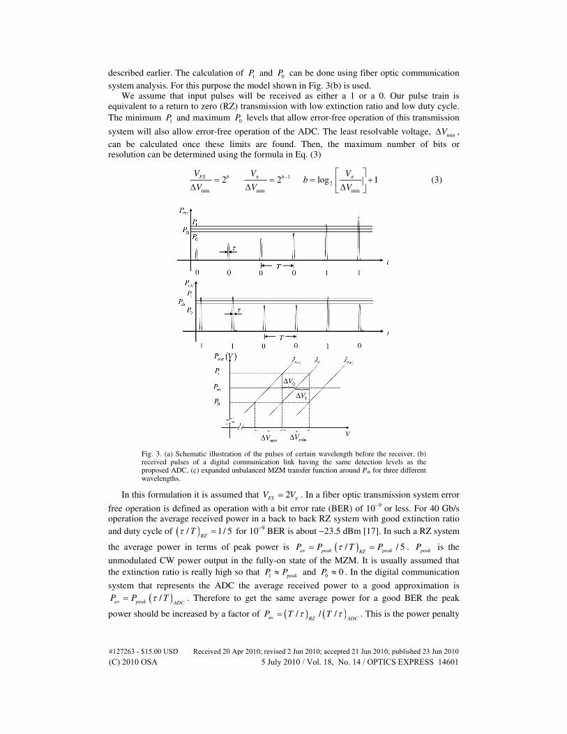
described earlier. The calculation of 1
P and 0
P can be done using fiber optic communication
system analysis. For this purpose the model shown in Fig. 3(b) is used. We assume that input pulses will be received as either a 1 or a 0. Our pulse train is
equivalent to a return to zero (RZ) transmission with low extinction ratio and low duty cycle.
The minimum 1
P and maximum 0
P levels that allow error-free operation of this transmission
system will also allow error-free operation of the ADC. The least resolvable voltage, min
V∆ ,
can be calculated once these limits are found. Then, the maximum number of bits or resolution can be determined using the formula in Eq. (3)
1
2
min min min
2 2 log 1b bFSV V Vb
V V V
π π− = = = + ∆ ∆ ∆
(3)
Fig. 3. (a) Schematic illustration of the pulses of certain wavelength before the receiver, (b) received pulses of a digital communication link having the same detection levels as the proposed ADC, (c) expanded unbalanced MZM transfer function around Pth for three different wavelengths.
In this formulation it is assumed that 2FS
V Vπ= . In a fiber optic transmission system error
free operation is defined as operation with a bit error rate (BER) of 10−9
or less. For 40 Gb/s operation the average received power in a back to back RZ system with good extinction ratio
and duty cycle of ( )/ 1 / 5RZ
Tτ = for 10−9
BER is about −23.5 dBm [17]. In such a RZ system
the average power in terms of peak power is ( )/ / 5av peak peakRZ
P P T Pτ= = . peak
P is the
unmodulated CW power output in the fully-on state of the MZM. It is usually assumed that
the extinction ratio is really high so that 1 peak
P P≈ and 0
0P ≈ . In the digital communication
system that represents the ADC the average received power to a good approximation is
( )/av peak ADC
P P Tτ= . Therefore to get the same average power for a good BER the peak
power should be increased by a factor of ( ) ( )/ / /av RZ ADC
P T Tτ τ= . This is the power penalty
#127263 - $15.00 USD Received 20 Apr 2010; revised 2 Jun 2010; accepted 21 Jun 2010; published 23 Jun 2010(C) 2010 OSA 5 July 2010 / Vol. 18, No. 14 / OPTICS EXPRESS 14601

due to low duty cycle. Typical ( )/ADC
T τ values are at the order of 25 and the corresponding
power penalty is about 7 dB. In addition for good resolution 1
P and 0
P should be close to one
another, i.e., extinction ratio should be low. Low extinction ratio introduces another power
penalty, exδ given in Eq. (4) as [18].
( ) ( )1 0 1 0/
exP P P Pδ = + − (4)
The average power must be increased by this factor to match the BER of the system with
high extinction ratio. Using the transfer function of the quantizer ( )1 1outP P V= and
( )0 0outP P V= , where 1
1 0 min/ 2b
V V V Vπ−− = ∆ = . Letting ( )/ 1 / 2n L mπ λ π∆ = + in
Eq. (1), we can express exδ as:
2 20 0
1
2 20 0
1
1cos cos
2 2 22
1cos cos
2 2 22
b
ex
b
V V
V V
V V
V V
π π
π π
π π π
δπ π π
−
−
+ +
=
+ −
(5)
Using this formula and 0
/ 2V Vπ= we estimate a power penalty of 13.5 dB for 6 bit
operation. Combining this penalty with the penalty of 7 dB for low duty cycle we get a total penalty of 20.5 dB. This is about the loss of 70 km of fiber. The ADC is therefore similar to a typical WDM communications link as far as power budgets are concerned. Error free
operation requires a received peak power of about −3 dBm or 0.5 mW. Assuming a 10 dB insertion loss for the quantizer, sampler and two AWGs, the required input power per channel is about 5 mW. This power is readily achievable using conventional laser diodes.
The temporal sampling method and parameters also affect ADC performance. According to a previous analysis of the proposed ADC based on signal-to-noise ratio calculations [8], the resolution and input power reported here are obtainable when sampling with a Gaussian aperture 5 ps wide (FWHM) and an rms jitter of 0.2 ps.
The spectral spacing and MZM length offset are also feasible. The spectral spacing must be large enough to avoid spectral overlap, and small enough to avoid significant dispersion in
Vπ that would lead to code nonlinearity. For a 20 GHz signal, the standard 100 GHz ITU
spacing should be sufficient. Sampling before demultiplexing increases each channel’s bandwidth, requiring increased channel spacing This spectral spacing determines the required length offset L∆ . For a given spectral grid, L∆ determines the spacing between transfer functions at different wavelengths along the voltage axis. Equal spacing is achieved if the
phase of the transfer function changes by ( )2 1 2m Nλϕ π∆ = + between two adjacent
channels separated in frequency by ν∆ , where 0m ≥ is an integer. Applying this condition
to Eq. (1):
( ) ( )2 1 / 2L c m nNλ ν∆ = + ∆ (6)
The voltage spacing between transfer functions must also be large enough to insure that only one channel at a time lies in the uncertain power region, as shown in Fig. 3. Choosing m to satisfy this condition leads to a L∆ ~200 µm. This offset is readily achieved by varying the half angles of the y-branch splitters of the MZM, as shown in Fig. 1. Additionally, a DC biased section in one arm could fine-tune the phase offset and stabilize the MZM during operation.
The source wavelengths may also drift. This increases exδ by shifting transfer functions
with respect to each other. For a typical wavelength-locked diode drift of 5 pm, exδ increases
by less than 1 dB based on Eq. (5). Therefore the ADC is robust to wavelength drift.
#127263 - $15.00 USD Received 20 Apr 2010; revised 2 Jun 2010; accepted 21 Jun 2010; published 23 Jun 2010(C) 2010 OSA 5 July 2010 / Vol. 18, No. 14 / OPTICS EXPRESS 14602

4. Conclusion
We introduce a novel photonic ADC design that resembles a WDM digital link with an unbalanced MZM between the transmitters and receivers. We show that the required MZM fabrication and WDM spectral grid are well within the capabilities of existing technology. A reasonable optical source power is predicted to deliver 6 bits of resolution at 40 GS/s. Higher sampling rates ~100 GS/s are possible due to the high bandwidth of MZMs.
Acknowledgements
This work was supported by National Science Foundation (NSF) Grant ECCS-0702087.
#127263 - $15.00 USD Received 20 Apr 2010; revised 2 Jun 2010; accepted 21 Jun 2010; published 23 Jun 2010(C) 2010 OSA 5 July 2010 / Vol. 18, No. 14 / OPTICS EXPRESS 14603


