A ‘Phase Reset’ Scheme for an 8-11Gb/s Bang-Bang CDR in ... · A ‘Phase Reset’ Scheme for...
66
A ‘Phase Reset’ Scheme for an 8-11Gb/s Bang-Bang CDR in 65nm CMOS by Ravi Shivnaraine A thesis submitted in conformity with the requirements for the degree of Masters of Applied Science Graduate Department of Electrical and Computer Engineering University of Toronto Copyright c 2013 by Ravi Shivnaraine
Transcript of A ‘Phase Reset’ Scheme for an 8-11Gb/s Bang-Bang CDR in ... · A ‘Phase Reset’ Scheme for...

A ‘Phase Reset’ Scheme for an 8-11Gb/s Bang-Bang CDR in
65nm CMOS
by
Ravi Shivnaraine
A thesis submitted in conformity with the requirementsfor the degree of Masters of Applied Science
Graduate Department of Electrical and Computer EngineeringUniversity of Toronto
Copyright c© 2013 by Ravi Shivnaraine

A ‘Phase Reset’ Scheme for an 8-11Gb/s Bang-Bang CDR in65nm CMOS
Ravi Shivnaraine
Master of Applied Science, 2013
Graduate Department of Electrical and Computer Engineering
University of Toronto
Abstract
This thesis presents the design and implementation of a CDR with ‘phase reset.’ By
continually ‘resetting’ the phase of the recovered clock to be aligned with data, cycle-
slipping and bit errors during the lock process are reduced. This concept was demon-
strated in a full-rate 8-11Gb/s Bang-Bang CDR in 65nm CMOS.
ii

Acknowledgements
I would like to thank my supervisor Professor Ali Sheikholeslami for his encourage-
ment and guidance. I’d also like to express my gratitude to Fujitsu labs for providing
their support and resources which made this work possible. Thanks to Professors David
Johns, Sean Hum, and Anthony Chan Carusone for serving on my thesis committee.
To my fellow group members Clifford and Sadegh thank you so much for the helpful
discussions and feedback which really helped to enhance this work and spawned ‘Clock
Phase Selection’ I mean ‘Embedded Frequency Detector.’ I’d also like to thank the folks
in BA5000 for making the office such a great place to work. Thanks to Colin, Mario
and Alireza for always being up for a ‘coffee run’, and to Shayan, Sadegh and Safeen for
always being up for a ‘< insert fun activity here > run.’ Thank you, Jaro Pristupa, who
always managed to bail us out when it felt like the sky was falling down (every month or
so). Many thanks to my family for supporting me throughout my degree. Lastly I’d like
to thank my closest group of friends, Starbucks, Mill St. Brewery and Johnnie Walker
who really helped to pull me through.
iii

Contents
1 Introduction 1
1.1 Motivation . . . . . . . . . . . . . . . . . . . . . . . . . . . . . . . . . . . 1
1.2 Thesis Objectives . . . . . . . . . . . . . . . . . . . . . . . . . . . . . . . 2
1.3 Thesis Outline . . . . . . . . . . . . . . . . . . . . . . . . . . . . . . . . . 2
2 Background 3
2.1 Overview of High-Speed Signaling . . . . . . . . . . . . . . . . . . . . . . 3
2.2 PLL-Based CDR . . . . . . . . . . . . . . . . . . . . . . . . . . . . . . . 5
2.2.1 Phase Detectors . . . . . . . . . . . . . . . . . . . . . . . . . . . . 7
2.2.2 Hogge PD . . . . . . . . . . . . . . . . . . . . . . . . . . . . . . . 7
2.2.3 Alexander PD . . . . . . . . . . . . . . . . . . . . . . . . . . . . . 8
2.2.4 Cycle Slipping . . . . . . . . . . . . . . . . . . . . . . . . . . . . . 9
2.3 Phase Interpolator CDR . . . . . . . . . . . . . . . . . . . . . . . . . . . 12
2.4 CDRs with Frequency Detector . . . . . . . . . . . . . . . . . . . . . . . 13
2.5 Burst-Mode CDRs . . . . . . . . . . . . . . . . . . . . . . . . . . . . . . 15
2.5.1 Single-Gated VCO . . . . . . . . . . . . . . . . . . . . . . . . . . 16
2.5.2 Phase Interpolating BM-CDR . . . . . . . . . . . . . . . . . . . . 17
2.6 Summary . . . . . . . . . . . . . . . . . . . . . . . . . . . . . . . . . . . 18
3 Proposed CDR Technique 19
3.1 Architecture . . . . . . . . . . . . . . . . . . . . . . . . . . . . . . . . . . 21
3.1.1 System Properties . . . . . . . . . . . . . . . . . . . . . . . . . . . 21
3.1.2 System Level Issue - Delay . . . . . . . . . . . . . . . . . . . . . . 24
3.2 Circuit Implementation . . . . . . . . . . . . . . . . . . . . . . . . . . . . 25
3.2.1 Delay Calibration . . . . . . . . . . . . . . . . . . . . . . . . . . . 26
3.2.2 Delay-Line . . . . . . . . . . . . . . . . . . . . . . . . . . . . . . . 28
3.2.3 Edge Generator . . . . . . . . . . . . . . . . . . . . . . . . . . . . 30
3.2.4 Gated-VCO . . . . . . . . . . . . . . . . . . . . . . . . . . . . . . 31
3.2.5 Tunable CDR Circuits . . . . . . . . . . . . . . . . . . . . . . . . 33
3.2.6 Core Programmability and Test-chip Overview . . . . . . . . . . . 34
3.3 System-Level Circuit Results . . . . . . . . . . . . . . . . . . . . . . . . . 36
3.4 Summary . . . . . . . . . . . . . . . . . . . . . . . . . . . . . . . . . . . 38
iv

4 Experimental Results 39
4.1 Receiver Layout and Equipment Setup . . . . . . . . . . . . . . . . . . . 394.2 VCO Tuning Range . . . . . . . . . . . . . . . . . . . . . . . . . . . . . . 414.3 Jitter Tolerance . . . . . . . . . . . . . . . . . . . . . . . . . . . . . . . . 424.4 Recovered Eyes & Jitter Breakdown . . . . . . . . . . . . . . . . . . . . . 434.5 Capture Range . . . . . . . . . . . . . . . . . . . . . . . . . . . . . . . . 454.6 Locking Performance . . . . . . . . . . . . . . . . . . . . . . . . . . . . . 464.7 Summary . . . . . . . . . . . . . . . . . . . . . . . . . . . . . . . . . . . 49
5 Conclusion 50
5.1 Thesis Contributions . . . . . . . . . . . . . . . . . . . . . . . . . . . . . 505.2 Future Work . . . . . . . . . . . . . . . . . . . . . . . . . . . . . . . . . . 51
5.2.1 Power Consumption Reduction . . . . . . . . . . . . . . . . . . . 515.2.2 Delay Sensitivity . . . . . . . . . . . . . . . . . . . . . . . . . . . 515.2.3 Phase Reset Auto Power-down . . . . . . . . . . . . . . . . . . . . 515.2.4 Half-Rate Operation . . . . . . . . . . . . . . . . . . . . . . . . . 515.2.5 ISI Sensitivity . . . . . . . . . . . . . . . . . . . . . . . . . . . . . 52
References 52
v

List of Tables
2.1 Alexander PD Truth-Table . . . . . . . . . . . . . . . . . . . . . . . . . . 9
4.1 Description of the pin-list . . . . . . . . . . . . . . . . . . . . . . . . . . 40
vi

List of Figures
2.1 Overview of a high-speed link . . . . . . . . . . . . . . . . . . . . . . . . 42.2 Clock & Data Recovery . . . . . . . . . . . . . . . . . . . . . . . . . . . . 42.3 VCO Based CDR Loop . . . . . . . . . . . . . . . . . . . . . . . . . . . . 52.4 Linearized Model of CDR Loop . . . . . . . . . . . . . . . . . . . . . . . 62.5 CDR Jitter Supression . . . . . . . . . . . . . . . . . . . . . . . . . . . . 62.6 Hogge Linear Phase Detector [8] . . . . . . . . . . . . . . . . . . . . . . . 82.7 Alexander (Bang-Bang) Phase Detector [11] . . . . . . . . . . . . . . . . 82.8 Locking Characteristic of CDR Loop . . . . . . . . . . . . . . . . . . . . 102.9 CDR loop is broken to observe PD behaviour in open-loop operation . . 102.10 Periodic Early/Late Pattern of Bang-Bang Phase Detector . . . . . . . . 112.11 Periodic Pattern of Charge-Pump Current for PRBS Input . . . . . . . . 112.12 Effect of CDR Loop Filter on CP Current . . . . . . . . . . . . . . . . . 122.13 Phase Interpolating CDR with Digital Loop Filter . . . . . . . . . . . . . 132.14 CDR loop with frequency detector . . . . . . . . . . . . . . . . . . . . . . 142.15 Data Driven Frequency Detector . . . . . . . . . . . . . . . . . . . . . . . 142.16 Reference based Frequency Detector . . . . . . . . . . . . . . . . . . . . . 152.17 Gated VCO Block Diagram & Operation . . . . . . . . . . . . . . . . . . 162.18 GVCO with control voltage regulated by PLL . . . . . . . . . . . . . . . 172.19 Phase Interpolating Burst-Mode CDR [19] . . . . . . . . . . . . . . . . . 18
3.1 Phase Reset Concept: Improved Bit-Lock Time & Control Voltage Settling 193.2 Timing transition from fast ‘bit-lock’ to steady state high jitter tolerance 213.3 Architecture of ‘phase reset’ with GVCO . . . . . . . . . . . . . . . . . . 223.4 Early/Late pattern for open-loop PD with ‘resets’ enabled . . . . . . . . 223.5 Biased charge-pump current with ‘resets’ enabled . . . . . . . . . . . . . 233.6 Behavioural results for #errors (Phase Reset vs. FD) . . . . . . . . . . . 233.7 Timing skew introduced after ‘reset’ . . . . . . . . . . . . . . . . . . . . . 243.8 Modified system to mitigate skew . . . . . . . . . . . . . . . . . . . . . . 243.9 Timing alignment after calibration . . . . . . . . . . . . . . . . . . . . . 253.10 System implementation of proposed system . . . . . . . . . . . . . . . . . 253.11 Block diagram of delay calibration loop . . . . . . . . . . . . . . . . . . . 273.12 Extracted simulation results of DLL . . . . . . . . . . . . . . . . . . . . . 283.13 Block diagram of delay-line . . . . . . . . . . . . . . . . . . . . . . . . . 293.14 Delay-line unit cell . . . . . . . . . . . . . . . . . . . . . . . . . . . . . . 293.15 Extracted results of delay-line . . . . . . . . . . . . . . . . . . . . . . . . 30
vii

3.16 Edge generator block diagram . . . . . . . . . . . . . . . . . . . . . . . . 303.17 Transient results (extracted) for edge generator . . . . . . . . . . . . . . 313.18 GVCO Block Diagram . . . . . . . . . . . . . . . . . . . . . . . . . . . . 313.19 Bias generator for GVCO . . . . . . . . . . . . . . . . . . . . . . . . . . 323.20 GVCO delay cell . . . . . . . . . . . . . . . . . . . . . . . . . . . . . . . 323.21 Extracted simulation results for GVCO tuning range . . . . . . . . . . . 333.22 CDR loop-filter with programmable current and variable resistor . . . . . 333.23 Programmable loop-filter resistor . . . . . . . . . . . . . . . . . . . . . . 343.24 Top-level block diagram of fabricated chip . . . . . . . . . . . . . . . . . 353.25 Test-chip register map block diagram . . . . . . . . . . . . . . . . . . . . 353.26 Simulated Locking Characterisitics . . . . . . . . . . . . . . . . . . . . . 363.27 Comparison of eye-diagrams from 3ns to 200ns . . . . . . . . . . . . . . . 373.28 Eye-diagram for CDR (‘reset’ off) near lock . . . . . . . . . . . . . . . . 373.29 Power consumption for ‘resetting’ power states . . . . . . . . . . . . . . . 38
4.1 Die Photo . . . . . . . . . . . . . . . . . . . . . . . . . . . . . . . . . . . 394.2 Equipment Setup . . . . . . . . . . . . . . . . . . . . . . . . . . . . . . . 414.3 Measured Power Consumption . . . . . . . . . . . . . . . . . . . . . . . . 414.4 VCO Tuning Range . . . . . . . . . . . . . . . . . . . . . . . . . . . . . . 424.5 Measured Jitter Tolerance . . . . . . . . . . . . . . . . . . . . . . . . . . 434.6 Retimed Eye with 10Gb/s PRBS7 Data . . . . . . . . . . . . . . . . . . . 434.7 Retimed Eye with 5Gb/s PRBS7 Data . . . . . . . . . . . . . . . . . . . 444.8 Jitter Breakdown . . . . . . . . . . . . . . . . . . . . . . . . . . . . . . . 444.9 BER with loop-back . . . . . . . . . . . . . . . . . . . . . . . . . . . . . 454.10 Measured Capture Range . . . . . . . . . . . . . . . . . . . . . . . . . . . 464.11 Bit-Lock Test Setup . . . . . . . . . . . . . . . . . . . . . . . . . . . . . 464.12 Bit-Lock Results . . . . . . . . . . . . . . . . . . . . . . . . . . . . . . . 474.13 VCO & With ‘Reset’ On & Off . . . . . . . . . . . . . . . . . . . . . . . 484.14 VCO Frequency over VDD . . . . . . . . . . . . . . . . . . . . . . . . . . 48
viii

List of Acronyms
BER Bit-Error Rate
BERT Bit-Error Rate Tester
BM-CDR Burst-Mode CDR
CDR Clock and Data Recovery
CP Charge-Pump
DFT Discrete Fourier Transform
DCDL Digitally Controlled Delay Line
DLL Delay Locked Loop
DMUX De-multiplxer
FD Frequency Detector
FPGA Field Programmable Gate Array
Gbps Ggigabits per second
GPON Gigabit Passive Optical Network
GVCO Gated Voltage Controlled Oscillator
ILO Injection Locked Oscillator
ISI Inter-Symbol Interference
MAC Media Access Control
PCIe Peripheral Component Interconnect
PCS Physical Coding Sub-layer
PD Phase Detector
PI Phase Interpolator
PIPE PHY Interface for PCI Express
ix

PLL Phase Locked Loop
PMA Physical Media Attachment
PRBS Pseudo Random Binary Sequence
UI Unit Interval
VCO Voltage Controlled Oscillator
x

1 Introduction
The growing need for bandwidth in internet applications increases the need for higher
aggregate data rate in both consumer and back-end communication links. Supporting
the demand is often accomplished by the use of multiple channels, and faster individual
lanes. Although an improvement in operating speed is important, it is also vital to limit
the rise in power consumption.
1.1. Motivation
To increase the overall power efficiency of transceivers, techniques involving a lower VDD
or current recycling [1] have been used. In situations where up to 90% of traffic is idle,
such as server applications [2], techniques that can allow for Clock and Data Recovery
(CDR) blocks to be turned on and off can be more effective than reducing the power
of circuit blocks. CDR circuits are typically built using phase tracking architectures
which offer high frequency jitter rejection and good jitter tolerance but are not easily
adaptable to applications requiring quick lock performance. Burst-Mode CDRs (BM-
CDRs) are typically used in applications where data is sent in packets (e.g. Passive
Optical Networks) and quick lock time is critical to reducing timing overhead. However,
unlike phase tracking CDRs they do not offer jitter rejection and good jitter tolerance
at high frequencies (near Nyquist). Applications requiring both rapid bit lock and good
steady state jitter performance fall into a void not adequately handled by either CDR
1

Chapter 1. Introduction 2
topology. To save power burst-mode techniques can be used to power-down circuit blocks
during periods of idle and save power. In this work a new CDR topology that exploits
the benefits of both phase tracking and BM-CDRs is proposed.
1.2. Thesis Objectives
This thesis presents a new CDR architecture to reduce the effects of cycle-slipping. The
main objectives of the thesis are as follows:
• Provide a background and a critique on different types of clock and data recovery
techniques
• Propose a ‘phase reset’ scheme as a novel clock recovery scheme
• Implementation details, circuit simulations, and measurements to prove function-
ality are provided
1.3. Thesis Outline
The remaining chapters of this thesis are organized as follows:
• Chapter 2 provides a background on phase-tracking and burst mode clock and data
recovery
• Chapter 3 describes the proposed CDR. A system level overview and circuit imple-
mentation of key blocks are shown as well as circuit simulation results
• Chapter 4 provides measurement results of the fabricated test chip
• Chapter 5 provides the future directions for this work

2 Background
This chapter presents the concepts and systems employed in clock and data recovery
circuits for binary signaling applications. Firstly, an overview of the CDR’s place within
a larger consumer application is discussed. The following sections provide an overview
of two general classes of CDRs the phase-tracking CDR and the burst-mode CDR. The
operation, performance metrics, circuit components and limitations of both types of
CDRs are introduced.
2.1. Overview of High-Speed Signaling
High-speed signaling applications which generally refer to rates above 1Gbps utilise serial
communication schemes to transmit data. Serial transmission of data avoids interconnect
overhead and skew caused by unequal bus lines or channel impairments. Serial schemes
generally fall into two broad categories, clock-forwarded links and embedded-clock links.
In clock-forwarded links a clock is sent with the data whereas embedded-clock links
only transmit data and the receiver must generate a clock to sample the data. Due
to additional power and interconnect overhead of forwarding the clock, embedded clock
links are widely used. An overview of a link between two high-speed interfaces is shown
in Figure 2.1. A typical standard compliant interface consists of three primary blocks.
First, the Media Access Control (MAC) controls speed/rate negotiation between the
two communication interfaces. The Physical Coding Sub-layer (PCS) is responsible for
3

Chapter 2. Background 4
channel encoding/decoding (e.g. 8B/10B, scrambling) and symbol alignment. Lastly,
the Physical Media Attachment (PMA) is the interface to the channel, which may be a
backplane or cable. The PMA performs two vital functions in the link. At the transmit
path, it takes parallel data from the PCS, serializes it and sends it across the channel. At
the receiver, the PMA generates a clock that is aligned to the data stream and samples
the incoming data. The sampled data, aligned to the local clock of the PMA is then
de-serialized and passed to the PCS for processing [3].
Interface #1 Interface #2TX
RX
RX
TX
MAC PCS PMA
TX
RX
Physical Layer
Figure 2.1: Overview of a high-speed link
The process by which the PMA generates a clock and samples data is typically referred
to as ‘Clock & Data Recovery.’ The primary challenge is generating a clock that is
aligned to the data stream, shown as Clock Recovery in Figure 2.2. Once a clock has
been generated the incoming data is simply sampled.
Clock
Recovery
D Q
DATA
FF
DATAREC
CLKREC
Figure 2.2: Clock & Data Recovery
The following sections introduce different examples of CDR circuits. First an overview

Chapter 2. Background 5
of phase-tracking CDRs [4–8] is done by examining a common Phase Locked Loop (PLL)
type CDR with Voltage Controlled Oscillator (VCO).
2.2. PLL-Based CDR
The main function of the PLL-based CDR is to zero the phase offset between clock &
data and re-time the data to the CDR’s local clock [9]. The CDR in Figure 2.3 uses
four components to accomplish this function. A Phase Detector (PD) is used to measure
the timing skew between the local clock, CKREC , and Data. The PD’s phase error
measurement is typically represented in two signals, in the diagram below, ‘Proportional’
and ‘Reference.’ The CDR’s charge-pump combines the information of these two signals
into one signal, typically a current, which is used to drive a filter (R, C1 & C2). The
CDR’s filter, commonly referred to as the ‘loop-filter’ integrates the charge-pump current
to produce a voltage which when applied to the voltage controlled oscillator varies the
phase and frequency of the recovered clock. The recovered clock is fed back to the phase
detector to continually refine the phase measurement.
Phase
Detector
Charge
Pump
Charge
Pump
DATA
DATAREC
CKREC
Proportional
Reference
VCO
R
C1
C2
Loop Filter
Figure 2.3: VCO Based CDR Loop
To model the behaviour of the closed loop system, a linear model as shown in Figure
2.4 is used. The CDR block diagram is replaced by a small-signal phase model of the
system. The ‘gain’ of the phase detector and charge-pump current are lumped into the
parameter KPD, and the loop-filter impedance is represented by the term L(s). The
change in VCO’s frequency due to a change in control voltage is modeled by KV CO.

Chapter 2. Background 6
Since the system modifies VCO frequency and not its phase directly, an integrating term
1/s is added to the VCO block [9, 10].
+ L(s)KPD KVCO/s+_
ΦRECΦERRΦIN
Figure 2.4: Linearized Model of CDR Loop
The closed loop transfer function of the CDR is shown below. This function is typ-
ically referred to as the CDR Jitter Transfer Function. C2 is ignored for simplicity but
does not significantly degrade the phase margin when set to be one-tenth of C1 [9]. In
applications requiring low jitter peaking C1 is often set to smaller ratios of C2.
ΦREC
ΦIN
= KPDKV CO1 + sRC1
C1s2 + sKPDKV CORC1 +KPDKV CO
(2.1)
Since the CDR’s phase response is low-pass in nature it does not respond to track high-
frequency jitter which results in the CDR suppressing high frequency jitter. This results
in the CDR being able to clean up data as shown in Figure 2.5 [9].
DATA
DATAREC
CLKREC
Figure 2.5: CDR Jitter Supression
One key metric of CDR systems is their tolerance to jitter. Jitter can be generally
classified as random or deterministic in nature [9]. Sources of random jitter are circuit
noise and power supply noise coupling. Deterministic jitter may be caused by Inter-
Symbol Interference (ISI) or periodic jitter sources [9]. One key figure of merit of a
CDR is its tolerance to sinusoidal jitter. From the jitter transfer characteristic of a PLL-

Chapter 2. Background 7
based CDR one can intuitively deduce its high frequency jitter tolerance is limited to
1UIp−p. This occurs because at high frequency the CDR is not able to track data, so
the maximum phase shift that can occur is 0.5UI to either edge of the sampling clock’s
location. This property of 1UIp−p jitter tolerance can also be seen by deriving the CDR’s
Jitter Tolerance function, which is the ratio of input phase, ΦIN , to the phase error,
ΦERR. |ΦERR| < 1UIp−p, for error free operation.
|ΦIN | =
∣
∣
∣
∣
1 +KPDKV CO (sRC1 + 1)
s2C1
∣
∣
∣
∣
(2.2)
As expected, replacing s = jw and letting w → ∞, |ΦIN | = 1. To complete the discussion
on phase tracking CDRs an overview of the phase detector and CDR loop dynamics is
discussed in the following sections.
2.2.1. Phase Detectors
Phase detectors can be broadly classified by the average output produced by their accom-
panying charge-pump. Phase detectors that produce a charge-pump current proportional
to the phase difference between clock and data are known as linear phase detectors, such
as the Hogge PD [8] shown in Figure 2.6. PDs like the Alexander [11] or Bang-Bang
phase detector produce a control signal based on the sign of the phase error and are
known as non-linear phase detectors.
2.2.2. Hogge PD
In the Hogge PD [8] (Figure 2.6) the reference pulse, REF , is generated by the XOR of
re-timed data on two edges. This pulse is referred to as a reference pulse because when
active it is always 1UI wide. The proportional, PROP , measures the relative phase error
by the XOR of the sampled data and the data signal itself. In the charge-pump the two
signals are subtracted and used to generate a control current. One drawback of the Hogge
PD is the CLK − to−Q delay of the first flop-flop compromises the phase measurement,

Chapter 2. Background 8
since the PROP signal is narrower than expected. Left uncompensated a phase error
can be introduced between clock & data [8, 12] which degrades jitter tolerance.
D Q D QDATA
CLKREC
REF
PROP
FF FF
Figure 2.6: Hogge Linear Phase Detector [8]
2.2.3. Alexander PD
The Alexander phase detector [11] in Figure 2.7 has gained popularity due to the fact that
both control signals ‘Early’ and ‘Late’ are exactly 1 UI which eliminates the systematic
offset present in linear phase detectors due to the asymmetric delays in the Proportional
and Reference paths.
D Q D Q
D Q D Q
CLKREC
DATA
Early
Late
FF FF
FF FF
Phase
Offset
Charge-Pump
Current
90° − 90°
D[n-1] D[n]
E[n]
Figure 2.7: Alexander (Bang-Bang) Phase Detector [11]
By comparing three evenly spaced samples the Alexander PD checks to see if the
data edge is before or after the clock edge, and generates a control signal to speed up or
slow down the VCO to ‘catch up to data.’ When locked, the PD’s samples correspond
to the current data bit, D[n], the previous data bit, D[n-1], and the data transition, E[n].
Shown in Table 2.1 is the truth table for the Alexander Phase detector.

Chapter 2. Background 9
Table 2.1: Alexander PD Truth-Table
DN−1 EN DN Decision
0 1 1 Late0 0 1 Early1 1 0 Early1 0 0 Late0 X 0 No Transition1 X 1 No Transition
2.2.4. Cycle Slipping
At the start of data communication, the frequency of the receiver clock and that of in-
coming data are different. Spread spectrum clocking (SSC) utilized in many applications,
is a common source of a frequency offset between clock and data. During a process which
is referred to as ‘pull in,’ the CDR adjusts the control voltage of its VCO so as to bring
the VCO frequency close to the data frequency. However, as the CDR control voltage
moves toward the direction of reducing the frequency offset, it may momentarily move
towards increasing the frequency offset. This process, which is caused by the periodic
output of the phase detector is referred to as cycle slipping [13]. Shown in Figure 2.8 is a
behavioural locking characteristic obtained by a SimulinkTM simulation of a PLL-based
CDR with Bang-Bang phase-detector.
Shown in 2.8, cycle slipping is illustrated by the control voltage, VCTRL, which re-
peatedly travels in the ‘wrong direction’ before settling to its correct value. At lock,
the loop transitions from a slow waxing and waning of charge-pump current to a high
frequency burst of alternating current which keeps the control voltage roughly constant.
Cycle slipping impacts the system in two different ways. It delays the time it takes the
control voltage to settle (frequency lock time) and delays the time it takes for bit-errors
to stop occurring (bit-lock time). In a phase tracking CDR both of these parameters are
coupled. Later it will be shown that the proposed scheme allows for correct phase align-
ment (bit-lock) even though frequency-lock has not yet been achieved. To understand

Chapter 2. Background 10
Control
Voltage
CP
Current
Bit
Errors
0 0.5 1 1.5 2 2.5 3
x 10-7
0.75
0.8
0.85
VCTRL
0 0.5 1 1.5 2 2.5 3
x 10-7
0
50
100
Bit Errors
0 0.5 1 1.5 2 2.5 3
x 10-7
-5
0
5x 10
-5 ICH
‘FREQUENCY LOCK’ TIME
‘BIT LOCK’ TIME
CYCLE SLIP
Time (s)
(V)
(A)
Figure 2.8: Locking Characteristic of CDR Loop
why the CDR cycle-slips, the phase detector’s transient behaviour in the presence of a
frequency offset is examined when the CDR loop is opened ( Figure 2.9).
Charge
Pump
Charge
Pump
DATA
CLKREC
Early
Late
VCO
Phase
Detector
Figure 2.9: CDR loop is broken to observe PD behaviour in open-loop operation
For the purpose of the discussion on cycle slipping the phase detector’s output for a
CDR with a Bang-Bang phase detector is examined since it is used in the implementation
of the proposed scheme. In the presence of a frequency offset the sampling position of the
clock slides across data. As shown below this sliding effect produces a periodic pattern
of Early and Late control signals. This result is expected since a frequency offset causes
a phase ramp between clock and data and the PD’s response repeats every 2π. However,
the periodicity of the PD output means when integrated by the loop filter, the CDR has
little to no information to act on for frequency acquisition. Additionally, depending on
the initial phase of the clock, the CDR temporarily moves against the direction of the

Chapter 2. Background 11
phase ramp.
(1)
(2)
(3)
(4)
(5)
(6)
(7)
(8)
Late
Late
Late
Late
Late
Early
Early
Early
5 Lates
3 Earlies
DATA
CLK
•••
Figure 2.10: Periodic Early/Late Pattern of Bang-Bang Phase Detector
The periodicity of charge-pump current was verified in a SimulinkTM behavioural
model and is shown in Figure 2.11 for various frequency offsets in the presence of a Pseudo
Random Binary Sequence (PRBS). In the presence of a frequency offset, the charge-pump
current is periodic and increases in frequency as the frequency offset increases.
0 0.2 0.4 0.6 0.8 1 1.2 1.4 1.6 1.8 2
x 10-7
-4
-2
0
2
4x 10
-4
Time(s)
CP
Cu
rre
nt (A
)
20 MHz
0 0.2 0.4 0.6 0.8 1 1.2 1.4 1.6 1.8 2
x 10-7
-4
-2
0
2
4x 10
-4
Time(s)
CP
Cu
rre
nt (A
)
50 MHz
0 0.2 0.4 0.6 0.8 1 1.2 1.4 1.6 1.8 2
x 10-7
-4
-2
0
2
4x 10
-4
Time(s)
CP
Cu
rre
nt (A
)
100MHz
0.2%
0.5%
1%
Figure 2.11: Periodic Pattern of Charge-Pump Current for PRBS Input
The PD’s demodulation property [10] of producing a periodic pattern proportional to
the frequency difference has a severe impact on the CDR’s tolerance to frequency offset

Chapter 2. Background 12
as illustrated in Figure 2.12. In the presence of a small frequency offset, the charge-pump
current is a low frequency pattern which is within the loop filter’s bandwidth. A large
frequency offset produces a rapidly changing charge-pump current which when integrated
by the loop filter leaves little information to drive the VCO.
Phase
Detector
Charge
Pump
Charge
Pump
Early
Late
DATA
CKREC
Early - Late
Small Offset
Large Offset
Before Loop Filter After Loop Filter
Figure 2.12: Effect of CDR Loop Filter on CP Current
Typically to reduce lock time, the CDR loop-bandwidth may be boosted to mitigate
the averaging effect of periodic PD output [4, 9]. Charge-pump current, which increase
loop gain and loop-bandwidth, is also typically increased during lock to push the CDR
quicker toward the settling point in the presence of cycle-slipping. However, this effect
saturates at some point because the CDR also moves in the wrong direction faster for
larger charge-pump currents. An important practical limitation of CDRs with only a
phase detector is their limited tolerance to frequency offset caused by cycle-slipping
[13]. To extend the CDR’s tolerance to frequency offset a frequency detector is often
incorporated into the CDR loop.
2.3. Phase Interpolator CDR
A common variant of the PLL-based CDR with passive loop-filter is the Phase Inter-
polating PLL-based CDR [4] as shown in Figure 2.13. The analysis and operation are
similar to the PLL-based CDR. In this CDR the phase of the recovered clock is discretely
controlled by the loop filter which sets a phase code rather than controlling oscillator fre-

Chapter 2. Background 13
quency as in Section 2.2. The analog loop filter is replaced by a digital loop filter, the
role of the analog loop filter components R and C1 are replaced by the gain block KP and
integral path respectively. The VCO from the analog loop filter is replaced by a phase
interpolator which mixes two quadrature reference clocks to produce the desired clock
phase. Since the system is missing the 1
sprovided by the VCO of the PLL-based CDR a
digital integrator is added to the proportional path before the phase code update block.
Ʃ
D QD Q
DMUX
KP
z-1
z-1
Phase
Update
KI
Phase
Interpolator
CLKI CLKQ
CLKREC
DATA
Centre
Edge
Integral Path
Proportional Path
1/KS
Early-Late CountSamplers
Figure 2.13: Phase Interpolating CDR with Digital Loop Filter
2.4. CDRs with Frequency Detector
A CDR’s lock range is typically on the order of its loop-bandwidth [9,13]. To expand the
CDR’s tolerance to frequency offset an auxiliary circuit known as a Frequency Detector
(FD) is added to the loop as shown in Figure 2.14 [9, 13].
The FD compares the frequency of the local clock to the data and provides a stim-
ulus to the VCO loop filter. Generally, during lock, the FD brings the VCO control
voltage close to the acquisition or pull-in range of the PD. At this point the FD stops
producing control signals and the PD eliminates any residual frequency offset. Since
during lock both frequency and phase detection loops are active the FD is designed to be
4-5× stronger than the phase detector so that it over-powers the phase detector during

Chapter 2. Background 14
Charge
Pump
Charge
PumpDATA
DATAREC
Early
Late
VCOPhase
Detector
Frequency
Detector
UP
DN
CLKI
CLKQ
Figure 2.14: CDR loop with frequency detector
frequency acquisition.
Rotational frequency detectors [12, 14] compare the movement of two quadrature
clocks relative to data. The FD in Figure 2.15 [14] operates by sampling two quadrature
phases of the local clock, CLKI and CLKQ and looking at their rotation. By comparing
the samples of CLKI as it changes from 1 → 0 (or 0 → 1) on the rising edge of the CLKQ
sample, the direction of frequency offset can be determined. When frequency is locked,
the FD detects no rotation and no further control pulses are generated. One draw-back
of this FD is that it requires 1
2UI spaced clocks, I and Q, which may be difficult to
generate and distribute. This presents further challenges when scaled to half-rate since
1
2UI spaced clocks translate to the need for 0o, 45o, 90o and 135o [6, 9]. Later it will
be shown that the proposed scheme can expand the CDR’s tolerance to frequency offset
(capture range) without the need for multiple phases of the clock.
D Q
D Q
D Q
FF FF
FF
UP
DNCLKI
CLKQ
DATA
Figure 2.15: Data Driven Frequency Detector

Chapter 2. Background 15
Figure 2.16 shows a reference based FD [9]. This type of FD compares the frequency
of the VCO to a fixed reference clock. The FD output may then drive the VCO through
the same path as the PD or may aid acquisition through an auxiliary path.
VCO
÷N
Decision
CircuitReference
Up/
Down
Figure 2.16: Reference based Frequency Detector
Although frequency detectors help the CDR to expand its lock range, they do not force
the CDR to be at or near correct sampling position throughout the locking process. In
the following section CDRs that directly force the sampling clock to the correct location
are explored.
2.5. Burst-Mode CDRs
Unlike a phase tracking CDR which produces a zero steady state phase error through
filtering and feed-back, Burst-Mode CDRs directly force the phase of the clock to be
aligned with data. This is accomplished by using an open-loop approach where the
clock is assumed to be in the correct position and its phase is not corrected or refined
through feedback. This section introduces two different types of Burst-Mode CDRs,
the Gated Voltage Controlled Oscillator (GVCO) and the Phase Interpolator (PI) BM-
CDR. Topologies like the Injection Locked Oscillator (ILO) [15] are also used, but do not
guarantee a 1UI bit-lock time.

Chapter 2. Background 16
2.5.1. Single-Gated VCO
One example of a Burst-Mode CDR is the single GVCO [16] shown in Figure 2.17 which
is a simplified version of the dual-gated VCO [17].
VCTRL
CLKREC
DATA
DATA
RESET
CLKREC
RESET
EDGE GENERATOR
½ UI
Gated VCO
Figure 2.17: Gated VCO Block Diagram & Operation
At a data edge a control signal, RESET , is generated and is used to control a gated-
oscillator. When high the oscillator is enabled, and when low the oscillator’s output is
a zero. When a data edge occurs, the gating circuit produces a RESET pulse that is
1
2UI wide. When RESET goes high, the oscillator resumes oscillation and produces a
rising edge at the centre of the data eye. Since the GVCO does not modify the recovered
clock frequency and only recovers the data’s instantaneous phase it achieves fast bit-lock,
but is unable to track drifts in the data frequency. In the absence of data transitions, a
frequency offset between clock and data shifts the CDR sampling position which limits the
CDR’s tolerance to continuous identical digits [18]. The GVCO frequency is set using
two techniques. Firstly, the GVCO’s control voltage is shared with a replica GVCO
in a PLL locked to an external reference, shown in 2.18. Mismatch between the two
GVCOs results in a static frequency offset between the local clock and data. Secondly,
the GVCO’s frequency is set using a frequency calibration loop. The frequency offset

Chapter 2. Background 17
produced in this scheme is limited by the resolution of the frequency calibration loop [18].
DATA
GVCO2
CLKREF
CLKTX
GVCO1
VCTRL
PLL
Clock
Recovery
CP &
LFPD
CLKREC
VCTRL
shared
Figure 2.18: GVCO with control voltage regulated by PLL
2.5.2. Phase Interpolating BM-CDR
Another approach to quickly recover data is the PI BM-CDR [19] shown in Figure 2.19.
This BM-CDR avoids the need for a replica PLL by mixing two reference clocks to
produce a clock aligned to data. To generate a clock aligned to the data edge the CDR
takes two samples, α and β of quadrature clocks CLKQ and CLKI respectively. Using
a phase interpolator the recovered clock is generated by mixing the samples with the
reference clocks, CLKREC(t) = βCLKQ(t) - αCLKI(t).
The PI BM-CDR achieves the same performance of a GVCO BM-CDR, but does
not suffer from the inherent frequency offset problem since it does not require replica
circuits. Drawbacks of the PI BM-CDR are its need for quadrature clocks which may
introduce difficulties in routing for multi-link systems. The PI BM-CDR also relies on
CMOS-level data to drive switches which may be difficult to attain at higher speeds, and
generating a CMOS-level data signal may generate a large delay between clock and data.
The implementation uses single transistor sample-and-hold circuits which also places
restrictions on the common-mode of clocks I and Q. Additionally, the sample-and-hold
circuits use a buffer to prevent kick-back, any gain introduced by the buffer modifies
the values of α and β and results in an incorrect value for the estimated phase of the

Chapter 2. Background 18
CKI
CKQ
CKREC
Dn Dn+1
CKI
CKQ
CKREC
t=t0
CKREC(t) = CKQ(t) − CKI(t) = CKI(t − t0)
= CKQ(t0)
= CKI(t0)
Phase Interpolator
CKI CKQ
CKRECData
CKI
CKQ
S/H
S/H
t-
Figure 2.19: Phase Interpolating Burst-Mode CDR [19]
recovered clock.
In the next chapter, we propose a concept to address limitations of lock-time in PLL-based
CDRs. Elements from PLL-based and BM-CDRs are employed to reduce CDR bit-lock
time to make the CDR more flexible in power-saving applications while maintaining a
theoretical 1UIp−p jitter tolerance after lock.
2.6. Summary
In this Chapter the PLL-based CDR and its limitations to cycle slipping have been
explored. The Burst-Mode CDR has been introduced, they offer faster lock time than
PLL-based CDRs but they suffer from limited to no jitter filtering and poor performance
at very high jitter frequencies. PLL based CDR offers good long term jitter stability
but suffers from slow lock-time due to cycle-slipping. BM-CDRs can lock fast which
is particularly useful in power-saving applications where blocks may be powered down
during periods of no data transmission.

3 Proposed CDR Technique
The proposed concept has two primary goals; firstly, to reduce the effect of cycle slipping
so the VCO control voltage settles faster to the correct value. The second is to avoid
bit errors that occur due to the cycle slipping effect of the clock sliding relative to data
during lock. Both goals are accomplished by the mechanism presented in Figure 3.1(a).
VCTRL
t
t
Accumulated Errors
Correct Trajectory
t
Accumulated Errors
VCTRL
t
CDR without Phase Reset CDR with ‘Phase Reset’
Unwanted
slip
Cycle-slipping reduced
Phase Error in Presence of Freq. Offset
Phase
Error
t
Reset
Interval
CDR with ‘Phase Reset’CDR Without Phase Reset
C D
E F
B
A
CP &
LF
Phase
Detector
DATA
CLKREC
DATAREC
VCTRL
VCO
+
ΦVCO
ΦRESET
ΦREC
Phase Reset
Figure 3.1: Phase Reset Concept: Improved Bit-Lock Time & Control Voltage Settling
19

Chapter 3. Proposed CDR Technique 20
Every few data edges, the phase of the local oscillator, ΦV CO is ‘reset’ to be aligned
with data. This is represented as the local oscillator, ΦV CO, being shifted by a correction
factor, ΦRESET such that the clock phase, ΦREC , is equal to the data phase. This work
uses a GVCO to completely reset the phase of the recovered clock, whereas the injection
locked technique presented in [20] uses a periodic injection of the reference clock to reduce
PLL phase noise.
Shown in Fig 3.1(b) is the phase error as a function of time for a CDR without phase
reset and for one with reset. In the former, the phase error changes sign every time it
grows to π, causing a cycle slip. In the latter, we reset the phase of the clock prior to the
phase error reaching π, hence avoiding the sign reversal and cycle slip. In other words,
in the CDR with phase resets, the phase detector produces an output with a non-zero
average, and is biased towards the direction of reducing frequency offset. Figure 3.1(c)
and (d) show the control voltage as a function of time for the CDR with and without
phase reset. Cycle slipping in the former delays the settling time of control voltage,
VCTRL, which increases frequency lock time, whereas the latter reduces frequency-lock
time. Another important consequence of avoiding cycle slips is the reduction in the
number of the errors produced in the CDR with phase reset. This is illustrated in Fig.
3.1(e) and (f).
The system uses an Alexander PD exploiting the fact that its output depends on the
sign of the phase error. This is desirable, since after a phase reset the PD can provide its
full-scale output to quickly catch up to the frequency offset. On the other-hand, after a
phase reset with a linear-phase detector the phase detector’s output would be near zero,
which would deteriorate the frequency lock time.
By resetting the phase of the clock to be aligned with data every few data edges the
CDR has similar limitations to that of a BM-CDR. Poor high frequency jitter tolerance
and degraded jitter filter occur because the CDR instantly reacts to data edges. To
achieve a quick lock time and good steady-state jitter performance, reset is disabled after

Chapter 3. Proposed CDR Technique 21
some time, tLOCK , as shown in Figure 3.2. Ideally the point at which the CDR transitions
from ‘quick lock mode’ to the ‘normal mode’ of operation would be automatic, but for
simplicity in this design tLOCK is chosen based on simulations of how long it takes the
CDR to settle for a given worst case frequency offset. A possible solution to determine
when a transition between quick lock and normal mode should be done is by utilising
a lock detector circuit. Using a digital loop filter as in Section 2.3, the output of the
integral counter can be monitored during the locking process. When the integral path
reaches a steady state value the CDR is roughly frequency locked.
t = 0
Quick Lock Mode
‘Reset’ Enabled
High Freq. Jitter Tolerance: ½ UI
CDR Settled
‘Reset’ Disabled
High Freq. Jitter Tolerance: 1 UI
t = tLOCK
Figure 3.2: Timing transition from fast ‘bit-lock’ to steady state high jitter tolerance
3.1. Architecture
To achieve a phase reset, a GVCO is inserted into a conventional CDR loop, shown in
Figure 3.3. The edge generator is used to control the number of resets that occur. On
a data edge a reset pulse, RESET , is used to restart the GVCO to be aligned with the
rising edge of data. Unlike a typical Burst-Mode CDR the frequency of the GVCO is
set via the feed-back loop of the CDR. The binary PD is unchanged from a conventional
system, and is still used to re-time data.
3.1.1. System Properties
To see the effects of phase resets on the phase detector’s output the CDR feedback
loop is broken. To compare the modified system with a conventional CDR, we repeat
the experiment of looking at the pattern of early and late events in the presence of a
frequency offset as shown in Figure 3.4. Data is slower than the clock (clock slides to the

Chapter 3. Proposed CDR Technique 22
DATA
DATAREC
Edge
Generator
UP
DN
Gated VCO
CP &
LF
CP &
LF
Phase
Detector
RESET
CLKREC
Figure 3.3: Architecture of ‘phase reset’ with GVCO
right of data) so ideally one would desire more down or late pulses to guide the CDR
in the direction of avoiding cycle-slipping. As shown in the example, on the fourth data
edge, a single phase reset is performed. At this point, the clock and data are aligned
and on the next clock edge, a correct decision of late is reached. Over the remaining
cycles the CDR continues to make a correct decision of late, and without a reset the
CDR eventually produces an early event. In this example of eight clock cycles, the PD’s
output has become biased in the direction of reducing cycle slipping with a phase reset
operation.
(1)
(2)
(3)
(4)
(5)
(6)
(7)
(8)
Late
Late
Late
Late
Late
Late
Late
Early
7 Lates
1 Early
Reset Aligns
Clock
DATA
CLK
Figure 3.4: Early/Late pattern for open-loop PD with ‘resets’ enabled
Figure 3.5 shows the results of a behavioural simulation performed in SimulinkTM ,
and demonstrates that the bias introduced is indeed dependent on the sign of the fre-
quency difference. Shown are behavioural simulation results for the CDR charge-pump

Chapter 3. Proposed CDR Technique 23
current when a phase reset is performed every 16 data edges for a PRBS31 data pat-
tern. In this simulation, it can be seen that the average current for the open-loop phase
detector has been modified to be biased toward the sign of the frequency offset.
0 0.2 0.4 0.6 0.8 1 1.2 1.4 1.6 1.8 2
x 10-7
-3
-2
-1
0
1
2
3
x 10-4
Time (s)
CP
Cu
rre
nt (A
)
Hybrid +150MHz Offset
0 0.2 0.4 0.6 0.8 1 1.2 1.4 1.6 1.8 2
x 10-7
-4
-2
0
2
4x 10
-4
Time (s)
CP
Cu
rre
nt (A
)
Hybrid -150MHz Offset
+ 1.5%
− 1.5%
Figure 3.5: Biased charge-pump current with ‘resets’ enabled
Shown in Figure 3.6 are the results of a behavioural simulation which compares a
frequency detector to phase resets in the presence of a 5% frequency offset. As discussed
previously, the FD is typically sized to have 4 to 5 times the gain of the PD path. For
a fair comparison phase resetting is also given a boost in charge-pump current during
pull-in. As shown phase reset is able to settle to a low Bit-Error Rate (BER) state well
before the CDR with FD loop.
0 1 2 3 4
x 10-7
0
100
200
300
400
500
600
700
800
900
1000
Time (s)
# E
rrors
Phase Reset
FD
0 1 2 3 4 5
x 10-7
0.55
0.6
0.65
0.7
0.75
0.8
0.85
0.9
0.95
Time (s)
VCTRL
Phase Reset
FD
Figure 3.6: Behavioural results for #errors (Phase Reset vs. FD)

Chapter 3. Proposed CDR Technique 24
3.1.2. System Level Issue - Delay
One of the limitations of the proposed system is delay. On a data edge there is some time
before the RESET pulse can toggle, tDATA−RESET . The clock buffers between the GVCO
and phase detector is another source of delay, tRESET−CLK . Other non-ideal sources of
delay such as limited bandwidth of the edge-generator and GVCO’s clock path may also
be present. These multiple delays (tDATA−RESET + tRESET−CLK) can be lumped into
one delay, tdelay, which exists between clock and data after a reset, as shown in Figure
3.7.
DATA
RESET
CLKREC
∆T1: Gating Pulse Width
∆T2: GVCO & Buffer
Delay
tdelay
Figure 3.7: Timing skew introduced after ‘reset’
To compensate for the timing skew, we add a delay line to the path between the
incoming data and the phase detector as shown in Figure 3.8.
DATA
DATAREC
Edge
Generator
UP
DN
Gated VCO
CP &
LF
CP &
LF
Phase
Detector
RESET
CLKREC
DATADELAYED
∆T
Figure 3.8: Modified system to mitigate skew
By inserting a delay here, the data is held while a reset operation is performed and
arrives at the phase detector such that DATADELAY ED and CLKREC are aligned, shown
in Figure 3.9. Ideally this delay (∆T) is equal to tdelay. We discuss the implementation
and calibration issues of the ∆T block later in section 3.2.1

Chapter 3. Proposed CDR Technique 25
DATA
RESET
CLKREC
DATADELAYED
Figure 3.9: Timing alignment after calibration
3.2. Circuit Implementation
The system implementation of the proposed concept in shown in Figure 3.10; highlighted
blocks are powered down during different phases of operation.
∆T
÷
DATA
PD & LF
DATAREC
÷8
CLKREC
VCOTEST
EDGE DETECTOR
Saturating
Counter
U/D
DIVIDER
REPLICA BLOCKS
DATADELAYED
‘RESET’
GVCOCDRENA
CDRENA
CAL
LINEENA
Select 4,8, or 16
CAL
R
CAL
R + CAL
DELAY
<3:0>CAL
0
1
0
1
1
0
CLKREC÷8
DELAY
LINE
CAL
Figure 3.10: System implementation of proposed system
To compensate for frequency offsets below 10%, the GVCO is reset every 4, 8 or
16 data rising edges. As mentioned earlier, without the delay line (∆T), after a reset,
some delay mismatch may exist between the recovered clock, CLKREC , and the data.
We mitigate this delay mismatch by the addition of the delay line (∆T) so that after
a reset, CLKREC is aligned with DATADELAY ED. To calibrate the delay line, a delay

Chapter 3. Proposed CDR Technique 26
control loop is incorporated into the system. During calibration (CDRENA = 0, CAL
= 1, R = 0), phase resets are not performed. In this mode, the CDR loop is opened
and a divided-by-8 version of the GVCO’s output is used as a ‘mock data source’. The
delay of the ∆T block is then compared to the delay of the reset operation. This is
achieved through bypassing the GVCO as the recovered clock and using the mock source
to exercise the edge-detector and GVCO’s gating logic delays. Since the GVCO is set
to free-run and acts as a data source, the delays of the edge-detector and GVCO gating
logic are accounted for through the use of replica blocks. The phase of the two paths is
compared by using the edge sample (U/D) of the bang-bang phase detector. The PD’s
edge sample is used as the Up or Down control of a saturating counter to adjust the
delay-line. After calibration is complete, the divider, replica blocks, and counter are all
powered down and the phase reset mode is enabled (CDRENA = 1, CAL = 0, R = 1).
Once the CDR achieves lock, the CDR is switched to normal operation (CDRENA =
1, CAL = 0, R = 0), and the edge detector is powered down. In steady-state (normal
operation), phase resets are not performed, the highlighted blocks are powered down, and
the control loop is identical to that of a conventional CDR. To characterize the GVCO’s
frequency and initialize the CDR to a fixed data rate for capture range measurements,
the loop filter switch, CDRENA, is used. During normal operation, the delay line is
kept on, bypassing the delay-line would save power during normal operation but it would
result in a few bit errors when switched off, to avoid this, a bypass was not included. To
characterize the power of the delay-line, a power down, LINEENA, was included.
3.2.1. Delay Calibration
As mentioned earlier the number of components used in the replica path was minimized
by passing the output of the replica blocks through the GVCO’s clock path. The delay
calibration loop (Figure 3.11) compares the phase of the ∆T block and reset path by re-
using the edge flip-flop of the Alexander phase detector. If the edge (Up/Down) signal

Chapter 3. Proposed CDR Technique 27
is 1 or 0 the delay of the ∆T block, a 4-bit Digitally Controlled Delay Line (DCDL) is
increased or decreased respectively. When the Up/Down signal toggles the calibration
has completed. The DCDL code D[3:0], is capable of being set externally by DEXT [3:0].
D Q
CLKREC
DATA
CP & LF
FF
DATAREC
D QD QD QD Q
CLK
EN
RESET
CML-to-
CMOS
D[3:0]
DEXT [3:0]
CLKCAL
UP/DOWN
UP/DOWN
D Q
D Q
D Q
Logic
CML-to-
CMOS
Saturating
Counter
Bang-Bang PD
Figure 3.11: Block diagram of delay calibration loop
Any residual error that may remain between ∆T and tdelay (delay of a reset operation)
causes an induced frequency offset, which we explain here. Consider the case of a conven-
tional CDR when locked. The CDR has an equal number of early and late events, and
on average maintains a constant control voltage. Adding phase resets periodically injects
a skew between clock and data, making the number of early and late events unbalanced.
To compensate, the CDR changes its frequency such that in the presence of a constantly
injected skew the number of early and late events is on average equal. This new locked
condition occurs because of an induced frequency offset. This is an unwanted effect, since
it is desired to disable ‘resetting’ after both frequency and phase are locked. Consider
the case if an induced frequency offset is produced; when phase resets are disabled the
conventional CDR loop must attain frequency lock which may result in cycle slipping
and bit errors. To mitigate the induced frequency offset, delay line resolution can be
increased or resetting phase may be performed less frequently. In this work we reset
phase less frequently, this is done by using a divider (by 4 or 8) in the edge generator.
By updating phase every nth data edge, a timing skew injected into the loop is averaged

Chapter 3. Proposed CDR Technique 28
over the longer reset period.
In Figure 3.12 are simulations results of the calibration loop (post-layout).
0
0.5
1
resetn
2
4
6
8
DL
L C
od
e
0
0.5
1
Up
/Do
wn
'
0 10 20 30 40 50 60 70 800
0.5
1
Time (ns)
CA
LCLK
Figure 3.12: Extracted simulation results of DLL
As expected the DLL loop’s control signal edge or Up/Down toggle when the system
is locked. However, given each delay code changes the phase by only a few picoseconds
the delay code drifts a few codes before toggling again. This occurs since the clock which
samples the mock data source is slower, and its rise/fall time causes inaccuracies when
sampling at the edge. This effect could have been reduced by averaging the edge samples,
but for simplicity the maximum and minimum values were simulated. The delay code at
the negative edge of Down (maximum number) was found to provide reliable results.
3.2.2. Delay-Line
The delay-line needs to compensate for roughly 300ps of delay, and must also have very
little ISI. One option is to use many CML stages and multiplex between them [15], but
this burns a significant amount of power. Phase mixing delay cells [21, 22] commonly
used for clocks were found to introduce a significant amount of jitter for the large delay
required, the same result was found for current-starved CMOS inverter delay chains as

Chapter 3. Proposed CDR Technique 29
used in [23]. The solution used (Figure 3.13) relied on CMOS inverters to buffer the signal
with low ISI and provide the bulk of the required delay with low power consumption.
The remaining delay was done with a manual CMOS delay and a 4-bit CML delay line.
A manual delay was used to provide a ±30ps delay shift primarily for process variation
and testing purposes.
DATA(t-∆t)
+
_DATA(t)
+
_
CML-to-
CMOS
Static CMOS Delay Adapted CML DelayManual Delay
shift[1:0] delay_code[3:0]
Figure 3.13: Block diagram of delay-line
Shown in Figure 3.14 is a unit CML-delay cell based on [7] used to construct the CML-
delay line. Complementary current sources are used to preserve the output common-
mode. By varying the current through the cross-coupled transistors the output resistance
of the cell is varied with varies its dominant pole and delay.
VOUT
+
_
+
_
VIN
RL RL
VBIAS
D3 D2 D1 D0 D3 D2 D1 D0
W2W4W8W W2W4W8W
Figure 3.14: Delay-line unit cell
Figure 3.15 are simulation results (post-layout) for delay code vs. delay for the nom-
inal case (shift = 2’b00) and ±30ps delay (shift 2’b01 and shift 2’b10, code 2’b11 was
not used).

Chapter 3. Proposed CDR Technique 30
0 5 10 15240
260
280
300
320
340
360
380
Delay Code
Dela
y (
ps)
Shift = 2'b00
Shift = 2'b01
Shift = 2'b10
Figure 3.15: Extracted results of delay-line
3.2.3. Edge Generator
To mitigate induced frequency offset and explore the relationship between capture range
and the frequency of phase resets a programmable divider chain was included (Figure
3.16). A state-machine that produced four outputs of divide by 2, 4, 8 and 16 was avoided
due to layout complexity. One important consideration of the divider chain is that the
outputs should have similar delays to avoid a wide tuning range in the delay line. On
the circuit level, the three have similar delays due to all clocks being generated by a
synchronous counter, during post-layout verification of the block delays were kept close
by routing each output to be roughly capacitance matched.
D Q D Q D Q D Q
DATA
÷4÷8÷16
÷2 Stage
FFFF FF FF‘EDGE’
SEL<2:0>
÷4
÷8
÷16
Figure 3.16: Edge generator block diagram
Shown in Figure 3.17 is a transient simulation (post-layout) of the divider outputs.

Chapter 3. Proposed CDR Technique 31
The outputs are selected via a 3-to-1 mux controlled via a one-hot control signal, sel[2:0].
The selected output goes to a pulse generator which uses symmetric XOR [24] to compare
the selected divider signal with a delayed version of the selected signal.
-1
0
1
Data
(V
)
-1
0
1
÷ 4
(V
)
-1
0
1
÷ 8
(V
)
0 1 2 3 4 5 6 7 8 9 10-1
0
1
Time (ns)
÷ 1
6 (
V)
Figure 3.17: Transient results (extracted) for edge generator
3.2.4. Gated-VCO
Figure 3.18 shows the functional diagram of the Gated-VCO. The gating block is built
using a 2-to-1 multiplexer which either passes the input from the VCO delay cells to the
output, starting oscillation, or passes ‘0’ to the output, stopping oscillation. The GVCO
delay cell is based on a differential pair with a cross-coupled stage.
VCTRL
CLKREC
‘RESET’
Single to
DifferentialVTUNE
+
_ ‘0’
0
1 +
_
+_
Figure 3.18: GVCO Block Diagram
The GVCO’s bias generator (Single to Differential, Figure 3.18) is shown in Figure
3.19. VCTRL steers current from the left and right branches of the PMOS differential

Chapter 3. Proposed CDR Technique 32
pair to produce two complementary reference currents for the VCO delay cells. The bias
voltage, VBIAS, is set by an on-chip current mirror and is used to bias other analog cells.
VCTRL
VTUNE
VBIAS
+
_
ITAIL
IL IR
CDC
Figure 3.19: Bias generator for GVCO
The GVCO delay cell [7] is shown in Figure 3.20. It is similar to the DCDL unit cell
but has analog current sources instead of digital current sources. Similarly to the DCDL
by varying the current through the cross-coupled transistors the output resistance of the
cell is varied which varies its dominant pole and delay. Complementary current sources
are used to preserve output common-mode.
VOUT
+
_
+_
VIN
RL RL
+
VTUNE
VBIAS
_
Figure 3.20: GVCO delay cell
The GVCO tuning characteristic (post-layout) is shown below. The GVCO has a
useful range of 7.8GHz to 10.5GHz. The system was designed for a centre frequency of
10GHz but due to a model change close to tape-out the centre frequency was reduced.

Chapter 3. Proposed CDR Technique 33
0 0.2 0.4 0.6 0.8 1 1.27.5
8
8.5
9
9.5
10
10.5
11
VCO Control Voltage (V)
Oscil
lati
on
Fre
qu
en
cy (
GH
z)
Figure 3.21: Extracted simulation results for GVCO tuning range
3.2.5. Tunable CDR Circuits
As mentioned previously the VCO control voltage, VCTRL, can be driven externally by
VINIT to initialize the CDR to a desired data rate, and characterize the GVCO without
the need for a replica GVCO break-out circuit. This is done using the programmable CP
and LF in Figure 3.22. Charge pump current can be divided by two or increased to vary
loop gain.
CP0 CP1 CP2 CP3
IUP
W 4W2WWW/2
ICP,NOM
UP
DOWN
IDN
VINIT
VCTRL
C1
C2R
VBP
VBN
CDC
RLIM
EN
EN
EN
EN
EN
EN
Figure 3.22: CDR loop-filter with programmable current and variable resistor
When the GVCO is driven externally by VINIT it is possible for drifts in the control
voltage to occur due to activity of the charge-pump. To avoid this effect, the charge-pump

Chapter 3. Proposed CDR Technique 34
bias voltages are gated. The loop filter resistance can also be varied to shift loop-filter
bandwidth if required, and the loop filter current can be digitally controlled. Shown in
Figure 3.23 is the control circuit for the loop-filter resistance.
R0 R1 R2 R3
+
_
RNOM
_
+
½ R
Figure 3.23: Programmable loop-filter resistor
The loop filter can be tuned from 10% of its nominal value. The control signals R3 to
R1 are set externally. Each resistor segment is composed of a resistance 1
2R, a 2R branch
is switched in-parallel with branches varying from 1.5R to 3R.
3.2.6. Core Programmability and Test-chip Overview
In Figure 3.24 is an overview for the fabricated system which includes the proposed CDR,
digital register interface and test structures. The digital interface allows for internal
power-downs, and programmable bits such as loop-filter resistance to be set without
requiring many I/Os. One important metric of the design is bit-lock time, but lock-time
is difficult to measure given our laboratory setup. To measure CDR lock time an on-chip
Bit-Error Rate Tester (BERT) was included, the BERT and DMUX circuit were modified
from earlier work by B. Abiri on a 1-6Gbps Phase Interpolating Burst-Mode CDR [19].
The BERT compares the incoming data to the expected patterns and produces a count
of the total number of errors. When the error counter stops accumulating the CDR has
achieved bit-lock. For the BERT output to be measured in the lab it is first down-sampled
by four, to be at a rate which is compatible with the synchronous sampling mode of the
laboratory logic analyzers. For testing purposes the number of errors from the BERT

Chapter 3. Proposed CDR Technique 35
can be observed or the real-time output of the delay calibration loop can be selected via
an output selector set through the digital control registers.
1:16
DMUXBERT 4
Control Registers
CDRDATA
DATARECCLKREC
D[15:0]
CLK/16
ERR[7:0]
CLK/16
CLK/64,ERRSAMP[7:0]
CLKCAL,UP/DN, DELAY[3:0]
DIG[7:0]
Output Select
PRBS7/31,
Reset Counter
Power Downs, DLL Reset, Delay
Code Overwrite, CP Bias, LF Resistor
ADR[2:0] DATA[3:0] REG_CLK[3:0]
CLK
Test Chip
Figure 3.24: Top-level block diagram of fabricated chip
Shown in Figure 3.25 is a functional diagram of the digital control interface. The
circuit has seven address banks each consisting of four data bits mapped to internal
control signals. The external signal ADR[2:0] which is mapped to one-hot bits ADRSEL
[6:0] is used to point to an internal register bank. WhenWRITEEN goes high the register
bank is set to WRDATA[3:0], and when WRITEEN is released the register bank clocks
itself.
DATA<3:0>
WRDATA<3:0>
ADRSEL<0> MEMCLK
LogicADR<2:0>
WRITEEN
ADRSEL<6:0>
D QD QD QD QFF
Figure 3.25: Test-chip register map block diagram

Chapter 3. Proposed CDR Technique 36
3.3. System-Level Circuit Results
Shown in Figure 3.26 are post-layout simulation results of the locking characteristic for
the CDR core. With a small frequency offset, 0.7%, the CDR with and without resets
enabled are compared. As shown without resets the CDR cycle clips and accumulates
many errors. With phase reset turned on the CDR does not cycle slip and bit errors
do not occur. A second locking characteristic simulation is also shown in Figure 3.26.
The CDR is initialized to 10Gbps and the input data is at 9.6Gbps, a 4% offset relative
to the local clock. Typically to boost the lock-range and reduce lock-time of a CDR its
charge-pump current is increased. In this simulation the CDR charge-pump current is
increased to eight times its nominal value. As shown the CDR loop without phase reset
never settles, and accumulates bit errors. With reset turned on, the CDR not only pulls
in, but there is little cycle-slipping and bit errors do not occur.
0.7%
Freq.
Offset
4%
Freq.
Offset
VCO Control Voltage Bit Errors
0 50 100 150 2000.68
0.685
0.69
0.695
0.7
0.705
0.71
Time (ns)
0 50 100 150 2000
5
10
15
20
25
30
35
Time (ns)
0 50 100 150 2000.64
0.65
0.66
0.67
0.68
0.69
0.7
0.71
0.72
0.73
Time (ns)
0 50 100 150 2000
50
100
150
200
250
300
Time (ns)
CDR Only vs. CDR with ‘Phase Reset’
Figure 3.26: Simulated Locking Characterisitics
Another way of looking at the locking speed of the CDR with phase reset is to compare
the eye diagrams of the recovered eyes during the lock process with phase reset on and off

Chapter 3. Proposed CDR Technique 37
(Figure 3.27). In both cases the eyes are plotted from 3ns to 200ns, sometime after the
first reset pulse arrive. In the eye-diagrams below the eye with reset on is fully opened
throughout the locking process compared to the conventional CDR.
0 100 200 300-0.8
-0.6
-0.4
-0.2
0
0.2
0.4
0.6
0.8
Time (ps)
Dif
fere
nti
al
Vo
ltag
e (
VPP)
'Reset' On
0 100 200 300-0.8
-0.6
-0.4
-0.2
0
0.2
0.4
0.6
0.8
Time (ps)
Dif
fere
nti
al
Vo
ltag
e (
VPP)
'Reset' Off
Figure 3.27: Comparison of eye-diagrams from 3ns to 200ns
Shown in Figure 3.28 is the retimed eye of the CDR (reset off) after 150ns. The
recovered eye is now open after the CDR control voltage has been able to settle.
0 50 100 150 200 250 300-0.8
-0.6
-0.4
-0.2
0
0.2
0.4
0.6
0.8
Time (ps)
Dif
fere
nti
al
Vo
ltag
e (
VPP)
Figure 3.28: Eye-diagram for CDR (‘reset’ off) near lock
Shown in Figure 3.29 is the simulated power consumption of the CDR core. During
delay calibration the system burns a peak power of 76mW, when resetting is active the
CDR dissipates 63mW and when disabled the CDR burns roughly 50mW. By powering
down the delay line, the CDR without any enhancements of resetting burns 33mW.

Chapter 3. Proposed CDR Technique 38
CAL
RESET
CDRENA
Mode
Estimated Power
∆T
Calibration
‘Phase
Reset’ ON
‘Phase
Reset’ OFF
76mW 63mW 51mW
Figure 3.29: Power consumption for ‘resetting’ power states
3.4. Summary
In this section the implementation details of the proposed concept were discussed. A
GVCO within a feedback loop is used to reduce the effects of cycle-slipping during the
lock process. Simulation results have shown that the concept achieves the desired func-
tionality and also reduces bit errors during lock. It was shown that a phase reset may
introduce a constant skew between clock and data which can reduce receiver performance.
To compensate for this effect a delay-line was inserted into the loop and a calibration
algorithm was designed to adjust its delay.

4 Experimental Results
4.1. Receiver Layout and Equipment Setup
Shown in Figure 4.1 is the die photo of the test-chip and the locations of key blocks.
CLKREC/8 +
AVSS
CLKREC/8 −
AVDDIO
DATA +
DATA −
AVSS
AVSS
AVDDCORE
AVDDCORE
IBIAS
AVSS
AVDDCORE
AVDDCORE
AVSS
N.C.
N.C.
AV
SS
RE
GCLK
AV
DD
CORE
AV
SS
WR
ITE
EN
AD
RSEL<
2>
AD
RSEL<
1>
AD
RSEL<
0>
WR
DATA<
3>
WR
DATA<
2>
WR
DATA<
1>
WR
DATA<
0>
N.C
.
AV
SS
AV
DD
CORE
N.C
.
AV
SS
DIGOUT<0>
AVSS
DIGOUT<1>
AVDDIO
DIGOUT<2>
DIGOUT<3>
AVSS
AVSS
CLKOUT
AVDDIO
DIGOUT<4>
AVSS
DIGOUT<5>
AVDDIO
AVSS
DIGOUT<6>
DIGOUT<7>
N.C
.
AV
DD
IO
AV
DD
IO
IBIA
SCP
AV
SS
IBIA
SDMUX
N.C
.
CLK
REC
+
AV
DD
IO
CLK
REC
−
VC
OTEST
DA
TA
REC
−
AV
SS
DA
TA
REC
+
AV
DD
IO
N.C
.
N.C
.
Active
CDR Core
375µm
600µm
200µm
Loop
Filter
PD &
G-VCO
Delay
Line
Replica
Blocks
Divider
On-chip
BERT
1
68
N
Figure 4.1: Die Photo
39

Chapter 4. Experimental Results 40
The test-chip was fabricated in Fujitsu’s 65nm CMOS process, the pad frame is
compatible with a 68-pin Cascade Microtech Z − Probecard c© and occupies an area of
2×2mm2. The CDR core occupies an area of 600×200µm2 and the loop-filter occupies
an area of 200×175µm2. A description of the pins shown in the die photo (Figure 4.1) is
provided in Table 4.1.
Pin name DescriptionDATA +/- Input data
DATAREC +/- Retimed dataCLKREC +/- Recovered clockCLKREC/8 +/- Recovered clock divided-by-8
REGCLK Register interface clock input (25MHz)WRITEEN Register write enable control
ADRSEL < 2 : 0 > Address select bitsWRDATA < 3 : 0 > Data input bitsDIGOUT < 7 : 0 > Digital output test bits (DLL Codes & BERT counter)
CLKOUT Digital output clockAVDDIO I/O Power Supply, 1.2VAVDD CDR Core Power Supply, 1.2VIBIAS 280µA reference current
IBIAS−DMX 400µA reference current for DMUX circuitsIBIAS−CP 25µA reference current for charge-pump
Table 4.1: Description of the pin-list
Figure 4.2 shows the equipment setup used during testing. A signal generator is used
as the clock source for BERT’s pattern generator. The CDR recovers the data from
the BERT, and outputs the retimed data and clock. The retimed data is viewed on an
oscilloscope, and the recovered clock’s frequency is verified using a spectrum analyzer.
Since the recovered clock is full rate, a divided by 8 version is included for cases where
the full-rate clock amplitude is too small for jitter measurements on an oscilloscope.
The delay-line calibration codes and bit-error counter value for the on-chip BERT are
available on the DIGOUT bus, which is monitored using a logic analyzer. Programming
of internal registers was performed using an FPGA. Three DC power supplies were used
to supply power rails and bias currents.

Chapter 4. Experimental Results 41
Signal Generator
BERT DUTLogic
Analyzer
FPGA
OscilloscopeSpectrum
Analyzer
Power
Supplies (x3)RFOUT
CLKIN
DATAOUT
DATAIN
DATAIN
DATAREC
CLKREC/8 CLKREC
CH1-CH3
CH2-CH4
REGINTERFACE
DIG[7:0],
CLKD
RFIN
PODA
REGCLK, ADRSEL[2:0], AVDD, AVDDIO, IBIAS, IBIASCP, IBIASDMX
JTAG, PC
WRDATA[3:0]
Figure 4.2: Equipment Setup
The measured power consumption of the CDR is shown in Figure 4.3. During delay-
line (∆T) calibration, phase reset on, and phase reset off modes the CDR consumes
84mW, 72mw and 48 mW respectively. The CDR power without the enhancement of
resetting (delay-line off) was measured to be 35mW. The measured power for the calibra-
tion phase and resetting enabled is higher than expected from simulated results shown
in Section 3, this may be due to inaccurate modeling of dynamic power, and inaccuracies
in recently updated transistor models.
CAL
RESET
CDRENA
Mode
Measured Power
∆T
Calibration
‘Phase
Reset’ ON
‘Phase
Reset’ OFF
84mW 72mW 48mW
Figure 4.3: Measured Power Consumption
4.2. VCO Tuning Range
To characterize the GVCO frequency within the CDR, the CDR loop is opened and
the GVCO control voltage is provided off-chip (CDRENA = 0, Figure 3.10). Measured
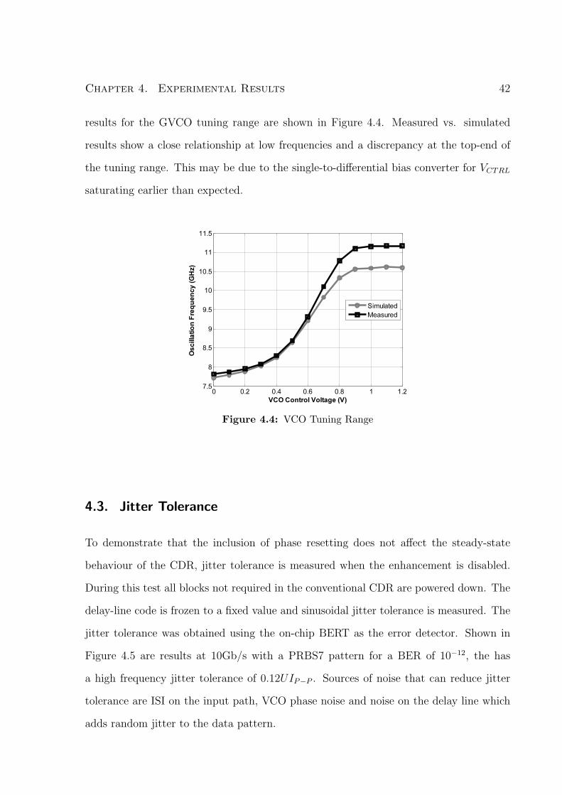
Chapter 4. Experimental Results 42
results for the GVCO tuning range are shown in Figure 4.4. Measured vs. simulated
results show a close relationship at low frequencies and a discrepancy at the top-end of
the tuning range. This may be due to the single-to-differential bias converter for VCTRL
saturating earlier than expected.
0 0.2 0.4 0.6 0.8 1 1.27.5
8
8.5
9
9.5
10
10.5
11
11.5
VCO Control Voltage (V)
Os
cilla
tio
n F
req
ue
nc
y (
GH
z)
Simulated
Measured
Figure 4.4: VCO Tuning Range
4.3. Jitter Tolerance
To demonstrate that the inclusion of phase resetting does not affect the steady-state
behaviour of the CDR, jitter tolerance is measured when the enhancement is disabled.
During this test all blocks not required in the conventional CDR are powered down. The
delay-line code is frozen to a fixed value and sinusoidal jitter tolerance is measured. The
jitter tolerance was obtained using the on-chip BERT as the error detector. Shown in
Figure 4.5 are results at 10Gb/s with a PRBS7 pattern for a BER of 10−12, the has
a high frequency jitter tolerance of 0.12UIP−P . Sources of noise that can reduce jitter
tolerance are ISI on the input path, VCO phase noise and noise on the delay line which
adds random jitter to the data pattern.

Chapter 4. Experimental Results 43
Jitter Frequency (MHz)
1 10
0.1
1
Jitte
r A
mplit
ude (
UI P
-P)
Figure 4.5: Measured Jitter Tolerance
4.4. Recovered Eyes & Jitter Breakdown
The full-rate retimed eye (Data sample from PD) is shown in Figure 4.6. A 10Gbps
PRBS7 pattern is used as an input to the CDR and the on-chip BERT shows no errors.
The oscilloscope using a 6MHz 2nd Order-PLL successfully locks onto the retimed eye,
and shows that a PRBS7 pattern is indeed being received. The recovered eye has a large
amount of jitter, 39psp−p, the recovered random jitter at a BER of 10−12 was measured
to be 1.21psrms and, 19ps of the retimed jitter, almost half, is due to ISI.
Figure 4.6: Retimed Eye with 10Gb/s PRBS7 Data
To verify that the recovered eye’s jitter is dominated by ISI (either due to the Probe-

Chapter 4. Experimental Results 44
Card and/or on-chip buffering to pads) a 5Gbps PRBS7 pattern is used as an input. In
this test the CDR is still operating at 10Gb/s but each bit is now twice as wide. The
re-timed eye (Figure 4.7) is now much more open, and has much sharper transitions
compared to the 10Gb/s eye.
Figure 4.7: Retimed Eye with 5Gb/s PRBS7 Data
The jitter breakdown of the 5Gb/s recovered eye is shown in Figure 4.8. The reduction
in total jitter, 39ps to 32.07ps is almost entirely due to the reduction in ISI, from 18.86ps
to 11.49ps.
Figure 4.8: Jitter Breakdown

Chapter 4. Experimental Results 45
To demonstrate CDR functionality without solely relying on the on-chip test circuits
a loop-back to the BERT’s error detector is performed. Two signal generators are syn-
chronized, one is used as the transmit clock for the BERT’s pattern generator and the
other clock is used as the BERT’s error detector clock. The error detector’s clock is
manually phase adjusted to be aligned with data, results are shown in Figure 4.9. At
10Gb/s the CDR obtained an error rate of 8.82−10, while the on-chip BERT showed no
errors. This may be caused by the small eye opening in the recovered eye due to ISI,
likely caused by on-chip buffers and the test setup. By reducing the data rate of the
input a reduction in BER was observed, and with a 5Gb/s (10Gb/s internal clocking)
input the CDR obtained an error rate better than 10−12.
10Gb/s
Input
5Gb/s
Input
Figure 4.9: BER with loop-back
4.5. Capture Range
The CDR was able to lock to data at 8 and 11Gb/s. Figure 4.10 shows the CDRs
measured capture range with and without resets at 10Gb/s. Since the lock-range of a
CDR is typically boosted by increasing its charge-pump current, the CDR capture range
was measured for 1×, 4× and 8× the nominal current of the charge-pump. The proposed

Chapter 4. Experimental Results 46
solution improves capture range by up to 5 times when phase resets are performed every
8 rising edges and up to 9 times when phase resets are performed every 4 rising edges.
1 4 80
2
4
6
8
10
Charge Pump Current/Nominal
Meas.C
aptu
re R
ange
(%
)
CDR without ‘Reset’
‘Reset every 8’ rising edges
‘Reset every 4’ rising edges
Figure 4.10: Measured Capture Range
4.6. Locking Performance
Figure 4.12 shows the total errors accumulated during the lock process. Due to mea-
surement limitations the errors during lock were recorded instead of bit errors vs. time
(bit-lock time). This measurement was performed using the on-chip BERT with 8-bit
error counter. The VCO frequency is initialized to a control voltage corresponding to
8.4GHz (8.4Gb/s) via V COTEST (see Figure 3.10) and the incoming data is set to various
frequency offsets. The CDRs loop-filter enable signal, CDRENABLE, and BERTRESET
are activated at the same time and the error count is observed, as shown in Figure 4.11.
CDRDATA On-Chip
DMUX
On-Chip
BERT
DATAREC
CLKREC
DATAREC[15:0]
CLKREC/16 #Errors [7:0]
BERT RESETCDRENA
CDRENA
Loop Filter Opened
VCO driven off-chip
BERT Counter Reset
Loop Filter Closed
BERT counts errors
t = 0
BERT RESET
CDR Locked?
BERT Reset Again
Errors = 0 (CDR Locked)
Errors = 255 (CDR Never Locks)Errors[7:0] shown below
•••
Figure 4.11: Bit-Lock Test Setup
With a frequency offset of 0.5% both with and without reset show no errors with a

Chapter 4. Experimental Results 47
charge-pump of 8×. The CDR without phase reset (‘no reset’) has errors at the lower
charge-pump currents, and phase resetting eliminates errors for all charge-pump currents.
At a frequency offset of 0.75%, the ‘no reset’ only locks when the charge-pump current
is increased to 4 or 8×. Even for the increased CP current, the error count is larger than
255. On the other hand, ‘reset every 8’ locks even with the 1× CP current. The ‘reset
every 4’ shows the best performance as it locks without any errors at all. With a 4%
frequency offset, ‘no reset’ does not achieve lock, ‘reset every 8’ locks but saturates the
error counter, and reset every 4’ produces as few as 25 errors with a charge-pump current
of 8× the nominal case.
Never Locks
Accumulated Errors
Locks,
Errors > 255
Locks,
Errors < 255
0 CP
Current1× 4× 8×
0.75%
Frequency
Offset
‘No Reset’
‘Reset every 8’
‘Reset every 4’
Accumulated Errors
0
217
4125
CP
Current1× 4× 8×
Never Locks
Locks,
Errors > 255
Locks,
Errors < 255
4%
Frequency
Offset
‘No Reset’
‘Reset every 8’
‘Reset every 4’
Accumulated Errors
0 CP
Current1× 4× 8×
Never Locks
Locks,
Errors > 255
Locks,
Errors < 255
0.5%
Frequency
Offset‘No Reset’
‘Reset every 8’‘Reset every 4’
103
17
Figure 4.12: Bit-Lock Results
The time at which phase reset could be turned off after the CDR loop was enabled
could not be experimentally tested due to an unexpected issue. To simplify the CDR
layout the VCO’s power supply was connected to the power supply of CDR core (PD,

Chapter 4. Experimental Results 48
Delay Line, Phase Reset Blocks). This was done because the IR drop in the presence
of blocks turning on and off was assumed to be very small, however, this was not the
case as shown in Figures 4.13 and 4.14. With phase reset on and off the VCO frequency
changes which introduces a frequency offset between clock and data, and temporarily
throws the CDR out of lock. This result was verified to be caused by the act of varying
the current drawn from VDD. By powering down blocks unrelated to both phase reset
and the conventional CDR a loss of lock was observed.
0 0.2 0.4 0.6 0.8 1 1.28
8.5
9
9.5
10
10.5
11
11.5
12
VCTRL
GV
CO
Fre
qu
en
cy (
GH
z)
'Reset' Off
'Reset' On
Figure 4.13: VCO & With ‘Reset’ On & Off
The effect of VDD on the VCO frequency can be see in Figure 4.14.
0 0.2 0.4 0.6 0.8 1 1.28
8.5
9
9.5
10
10.5
11
11.5
12
VCO Control Voltage (V)
Oscil
lato
r F
req
uen
cy (
GH
z)
VDD
= 1.1V
VDD
= 1.2V
VDD
= 1.3V
Figure 4.14: VCO Frequency over VDD

Chapter 4. Experimental Results 49
4.7. Summary
In this section the measured results of the fabricated 65nm test-chip were shown. The
CDR successfully operates over a range of 8-11Gb/s and achieves a BER of better than
10−12. The enhancement of phase resetting achieves an up to 9× improvement in CDR
capture range and significantly boosts the error free lock range of the CDR. The steady-
state power incurred to have the enhancement of phase reset is 15mW.

5 Conclusion
5.1. Thesis Contributions
This thesis provided an overview of CDR topologies. Phase tracking and Burst-Mode
CDRs were explored. Phase tracking systems have good jitter performance and slow lock
time versus BM-CDRs which have poor jitter performance and fast lock time.
The work presented in this thesis place a GVCO within a phase tracking CDR to
speed up lock time and reduce cycle slipping. Resetting of the GVCO can be halted after
lock to operate the CDR as a conventional loop and achieve good jitter performance. The
test-chip was fabricated in Fujitsu’s 65nm process and demonstrated a 9× improvement
in CDR capture range. The concept was also shown to reduce the number of errors during
the lock process. The inclusion of phase reset blocks did not hinder the standalone CDR
performance and, the CDR achieved a BER of better than 10−12 at 10Gb/s.
A summary of the contributions are:
1. Test-chip fabricated in 65nm CMOS at the intended 10Gb/s centre frequency.
2. Paper submitted to the IEEE Journal of Solid State Circuits (JSSC) in November,2012, [25].
50

Chapter 5. Conclusion 51
5.2. Future Work
The main enhancements that can be added to this work are summarized below;
5.2.1. Power Consumption Reduction
One major source of power consumption in the current implementation is the delay-
line (∆T) which is used to mitigate skew between clock and data after a phase reset.
This block consumes roughly 15mW. This was required to achieve three main design
requirements, high bandwidth (low ISI), a relatively large static delay of 300ps, and
delay tuning. A low power delay-line that offers wide delay tuning and low ISI is a key
step in reducing overall power consumption.
5.2.2. Delay Sensitivity
The sensitivity to a phase error after a phase reset required the addition of a power hungry
delay-line, which required a large delay calibration loop. Both of these components
increased power consumption and increased design complexity. A system modification
to reduce the need for a delay-line would reduce complexity and save power.
5.2.3. Phase Reset Auto Power-down
In the work resets are disabled a fixed time after the CDR is enabled. The time to
disable resets can be determined by simulating the CDR loop and choosing a time which
is larger than the expected settling time. However, this may result in phase resets being
performed for longer than required, which increases the overall power consumption of the
CDR. By incorporating a lock detector into the CDR the time to disable resets can be
determined as the CDR is running.
5.2.4. Half-Rate Operation
To further reduce power consumption a topology that supports half-rate clocking can be
used. Operating at half-rate would require the phase-reset blocks to monitor the phase

Chapter 5. Conclusion 52
of the recovered clock to either generate a rising or falling edge depending on the current
clock phase when a result pulse is generated.
5.2.5. ISI Sensitivity
The proposed architecture in this paper assumes a front-end equalizer that provides some
equalization in order to clean the jitter in the data and boosts its transitions. Not having
an equalizer in the front end may result in increased BER due to two different phenomena.
First, since the system uses the data rising edge to perform a phase reset, ISI may lead to
different delays through the reset path and delay line. This delay mismatch can introduce
a timing skew, which as discussed earlier, can induce a frequency offset, and cause cycle
slipping and bit errors when phase reset is turned off. Second, the timing skew between
the two paths may also shift the CDR sampling position during lock, which may result
in more bit errors during pull-in. This effect may be mitigated by resetting phase less
frequently, but this may add more latency to the reset path and necessitate a large delay
line.

References
[1] R. Inti, A. Elshazly, B. Young, Wenjing Yin, M. Kossel, T. Toifl, and P.K. Hanu-
molu. A highly digital 0.5-to-4gb/s 1.9mw/gb/s serial-link transceiver using current-
recycling in 90nm cmos. In Solid-State Circuits Conference Digest of Technical Pa-
pers (ISSCC), 2011 IEEE International, pages 152 –154, feb. 2011.
[2] J.G. Koomey, S. Berard, M. Sanchez, and H. Wong. Implications of historical trends
in the electrical efficiency of computing. Annals of the History of Computing, IEEE,
33(3):46 –54, march 2011.
[3] PHY Interface for the PCI Express, SATA and USB 3.0 Architectures. 2011.
[4] M. Pozzoni, S. Erba, P. Viola, M. Pisati, E. Depaoli, D. Sanzogni, R. Brama,
D. Baldi, M. Repossi, and F. Svelto. A Multi-Standard 1.5 to 10 Gb/s Latch-Based
3-Tap DFE Receiver With a SSC Tolerant CDR for Serial Backplane Communica-
tion. Solid-State Circuits, IEEE Journal of, 44(4):1306 –1315, april 2009.
[5] C. Kromer, G. Sialm, C. Menolfi, M. Schmatz, F. Ellinger, and H. Jackel. A 25-Gb/s
CDR in 90-nm CMOS for High-Density Interconnects. Solid-State Circuits, IEEE
Journal of, 41(12):2921 –2929, dec. 2006.
[6] J. Savoj and B. Razavi. A 10 Gb/s CMOS clock and data recovery circuit with
frequency detection. In Solid-State Circuits Conference, 2001. Digest of Technical
Papers. ISSCC. 2001 IEEE International, pages 78 –79, 434, 2001.
53

References 54
[7] Bahzad Razavi. Design of Analog CMOS Integrated Circuits. McGraw-Hill Science,
2001.
[8] Jr. Hogge, C. A self correcting clock recovery curcuit. Lightwave Technology, Journal
of, 3(6):1312–1314, december 1985.
[9] Bahzad Razavi. Design of Integrated Circuits for Optical Communications. McGraw-
Hill Science, 2002.
[10] Johns D.A and K. Martin. Analog Integrated Circuit Design. Wiley & Sons, 1996.
[11] J.D.H. Alexander. Clock recovery from random binary signals. Electronics Letters,
11(22):541–542, 30 1975.
[12] A. Pottbacker, U. Langmann, and H.-U. Schreiber. A Si bipolar phase and frequency
detector IC for clock extraction up to 8 Gb/s. Solid-State Circuits, IEEE Journal
of, 27(12):1747 –1751, dec 1992.
[13] Gardner F.M. Phase-Locked Loops, Second Ed. New York: Wiley & Sons, 1979.
[14] R.C.H. van de Beek, C.S. Vaucher, D.M.W. Leenaerts, E.A.M. Klumperink, and
B. Nauta. A 2.5-10-GHz clock multiplier unit with 0.22-ps RMS jitter in standard
0.18- µm CMOS. Solid-State Circuits, IEEE Journal of, 39(11):1862 – 1872, nov.
2004.
[15] Jri Lee and Mingchung Liu. A 20-Gb/s Burst-Mode Clock and Data Recovery
Circuit Using Injection-Locking Technique. Solid-State Circuits, IEEE Journal of,
43(3):619–630, march 2008.
[16] M. Nogawa, K. Nishimura, S. Kimura, T. Yoshida, T. Kawamura, M. Togashi,
K. Kumozaki, and Y. Ohtomo. A 10 Gb/s burst-mode CDR IC in 0.13 µm CMOS.
In Solid-State Circuits Conference, 2005. Digest of Technical Papers. ISSCC. 2005
IEEE International, pages 228–595 Vol. 1, feb. 2005.

References 55
[17] M. Banu and A. Dunlop. A 660Mb/s CMOS Clock Recovery Circuit with Instanta-
neous Locking for NRZ Data and BurstMode Transmission. In Solid-State Circuits
Conference Digest of Technical Papers (ISSCC), pages 102–103, 1993.
[18] J. Terada, K. Nishimura, S. Kimura, H. Katsurai, N. Yoshimoto, and Y. Ohtomo.
A 10.3125Gb/s Burst-Mode CDR Circuit using a δσ DAC. In Solid-State Circuits
Conference, 2008. ISSCC 2008. Digest of Technical Papers. IEEE International,
pages 226 –609, feb. 2008.
[19] B. Abiri, R. Shivnaraine, A. Sheikholeslami, H. Tamura, and M. Kibune. A 1-to-
6Gb/s phase-interpolator-based burst-mode CDR in 65nm CMOS. In Solid-State
Circuits Conference Digest of Technical Papers (ISSCC), 2011 IEEE International,
pages 154–156, feb. 2011.
[20] Ye. Sheng, L. Jansson, and I. Galton. A multiple-crystal interface pll with vco re-
alignment to reduce phase noise. Solid-State Circuits, IEEE Journal of, 37(12):1795
– 1803, dec 2002.
[21] B. Lai and R.C. Walker. A Monolithic 622Mb/s Clock Extraction Data Retiming
Circuit. In Solid-State Circuits Conference, 1991. Digest of Technical Papers. 38th
ISSCC., 1991 IEEE International, pages 144 –306, feb 1991.
[22] S.K. Enam and A.A. Abidi. NMOS IC’s for clock and data regeneration in gigabit-
per-second optical-fiber receivers. Solid-State Circuits, IEEE Journal of, 27(12):1763
–1774, dec 1992.
[23] I. Ahmed and D.A. Johns. A High Bandwidth Power Scalable Sub-Sampling 10-
Bit Pipelined ADC With Embedded Sample and Hold. Solid-State Circuits, IEEE
Journal of, 43(7):1638 –1647, july 2008.

References 56
[24] D. Rennie and M. Sachdev. A 5-Gb/s CDR Circuit With Automatically Calibrated
Linear Phase Detector. Circuits and Systems I: Regular Papers, IEEE Transactions
on, 55(3):796–803, april 2008.
[25] Ravi Shivnaraine, Mohammed Sadegh Jalali, Ali Sheikholeslami, Masaya Kibune,
and Hirotaka Tamura. A ‘Phase Reset’ Scheme for an 8-11Gb/s Bang-Bang CDR.
Solid-State Circuits, IEEE Journal of (submitted in Nov. 2012).