A PeakForce KPFM study in a controlled
35
Mapping Graphene’s surface potential with <20nm resolution: A PeakForce KPFM study in a controlled <1ppm water and oxygen environment Greg Andreev and Aravind Vijayaraghavan 9/27/13
Transcript of A PeakForce KPFM study in a controlled

Mapping Graphene’s surface potential with <20nm resolution: A PeakForce KPFM study in a controlled <1ppm water and oxygen environment Greg Andreev and Aravind Vijayaraghavan 9/27/13

Webinar Outline
• Introduction to Graphene by Aravind • Introduction to PF-KPFM • Results on Graphene in Air and Glovebox • Questions
10/7/2013 2 Bruker Nano Surfaces
Potential
250nm -100mV
100mV
An introduction to graphene
and the importance of environment
Dr. Aravind Vijayaraghavan
The University of Manchester
Bruker Webinar "Mapping Graphene’s Surface
Potential with less than 20nm Resolution"

WHAT IS GRAPHENE
Graphene is
imensional
Buckyballs Carbon Nanotubes Graphite A. K. Geim, K. S. Novoselov
Nat Mater 2007, 6, 183.

HOW TO MAKE GRAPHENE
1. Micromechanical cleavage of Graphite
(a) Attach a piece of graphite
to sticky-tape (Cellotape)
(b) Use the sticky tape to thin
out the graphite
(c) Place the thin graphite on
a Silicon wafer, with a
surface layer of Silicon
Dioxide
(d) Remove most layers of
graphite leaving behind
graphene.

HOW TO MAKE GRAPHENE
2. Chemical Vapour deposition(a)Carbon atoms are
deposited on the surface
of a metal
(b)At high temperature this
forms graphene.
(c) A layer of polymer is
deposited on top of the
graphene.
(d)The polymer is removed
and the graphene with it.
(e)The polymer is placed on
a suitable substrate
(f) The polymer is dissolved
away leaving the
graphene behind.

HOW TO FIND GRAPHENESeeing is believing!
P. Blake, et al., Appl. Phys. Lett. 2007, 91, 063124.

ELECTRONIC STRUCTURE
Monolayer Graphene
Electronically, monolayer, bilayers and trilayer graphene are electronically
distinct materials. Beyond three layers, graphene’s electronic properties
tends towards that of bulk graphite.
T. Ohta, et al., Science 2006, 313, 951.
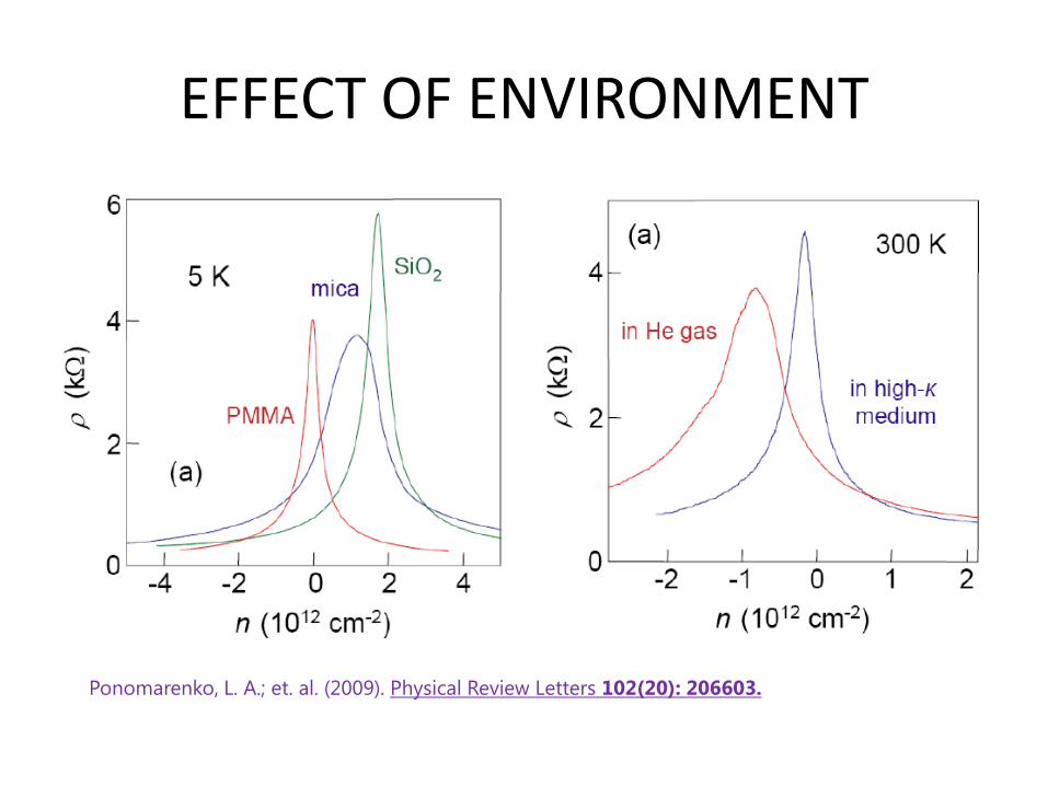
EFFECT OF ENVIRONMENT
Ponomarenko, L. A.; et. al. (2009). Physical Review Letters 102(20): 206603.

EFFECT OF DOPING
Changes in resistivity, at zero B
caused by graphene’s exposure to
various gases diluted in
concentration to 1 p.p.m. The
positive (negative) sign of changes
is chosen here to indicate electron
(hole) doping.
Region I: the device is in vacuum
before its exposure;
II: exposure to a 5 l volume of a
diluted chemical;
III: evacuation of the experimental
set-up; and
IV: annealing at 150 C.
Schedin, F., et al (2007). Nature Materials, 6(9), 652-655.
3
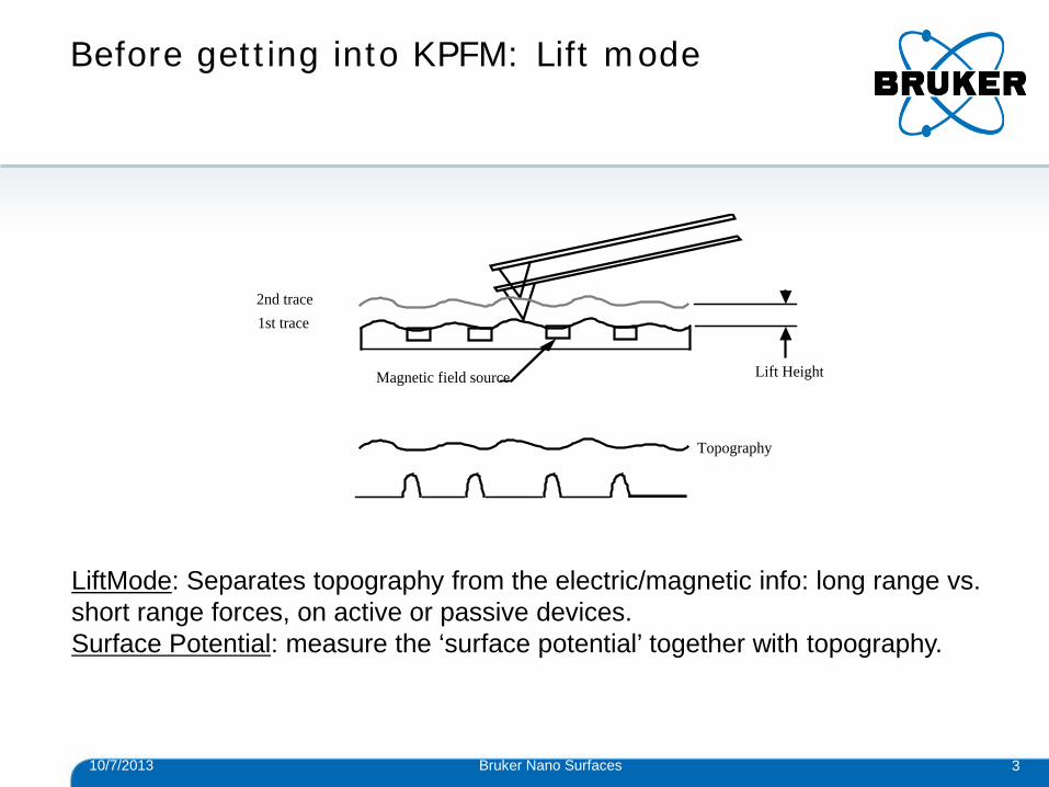
2nd trace1st trace
Lift Height
Topography
Magnetic field source
LiftMode: Separates topography from the electric/magnetic info: long range vs. short range forces, on active or passive devices. Surface Potential: measure the ‘surface potential’ together with topography.
Before getting into KPFM: Lift mode
10/7/2013 Bruker Nano Surfaces
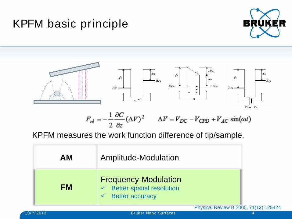
KPFM basic principle
AM Amplitude-Modulation
FM Frequency-Modulation Better spatial resolution Better accuracy
Physical Review B 2005, 71(12) 125424
KPFM measures the work function difference of tip/sample.
Bruker Nano Surfaces 10/7/2013 4

Many Ways of Doing KPFM FM and PeakForce scaling do not compete
AFM KPFM Tapping PeakForce
AM TP-AM PeakForce KPFM-AM
FM TP-FM PeakForce KPFM
Bot
h A
M &
FM
KP
FM
impr
oves
with
low
er k
Tapping is limited to high k levers due to adhesive forces. PeakForce Tapping k is not.
*Except TP-FM, all are done in lift-mode. 10/7/2013 Bruker Nano Surfaces 5
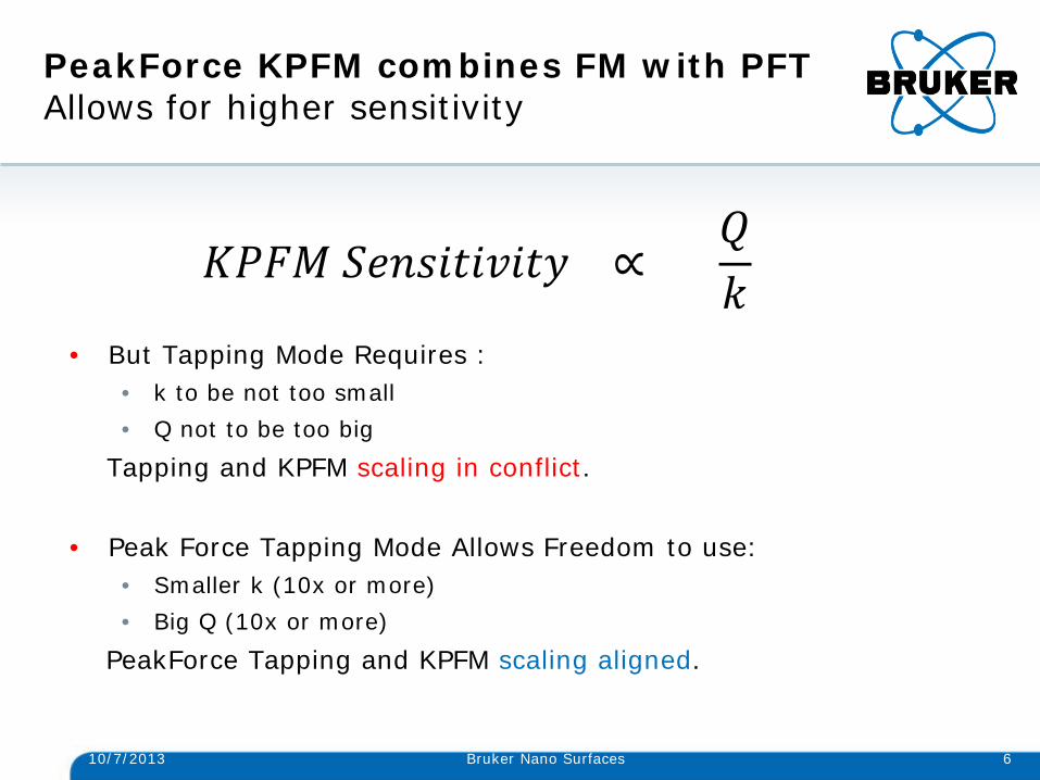
PeakForce KPFM combines FM with PFT Allows for higher sensitivity
• But Tapping Mode Requires : • k to be not too small • Q not to be too big
Tapping and KPFM scaling in conflict.
• Peak Force Tapping Mode Allows Freedom to use: • Smaller k (10x or more) • Big Q (10x or more)
PeakForce Tapping and KPFM scaling aligned.
10/7/2013 6 Bruker Nano Surfaces
𝐾𝐾𝐾𝐾 𝑆𝑆𝑆𝑆𝑆𝑆𝑆𝑆𝑆𝑆𝑆 ∝ 𝑄𝑘

KPFM: nanoscale measurement of Work Function, Fermi Energy & Carrier Density
• Previous work shows Work Function relationship to Efermi for Graphene
Bilayer
Single layer
KPFM can be used as a nanoscale measurement of Fermi energy
Y. Yu et. al. NanoLett. (9) 10 – 2009
10/7/2013 Bruker Nano Surfaces 7

Energy diagram of our KPFM experiment on Graphene
10/7/2013 Bruker Nano Surfaces 8
𝑊smp 𝑊elec
𝑆∆𝑉𝑉𝐾𝑉
𝑊tip
What KPFM measures
Vacuum level
𝑊0gr ~ 4.6eV
𝑊tip ~ 4.5eV
𝑊elec ~ 4.9eV
𝑊a ~ 0.05eV
𝐸F ~±0.3eV
Approx. Values
𝐸F
𝑊0gr
𝑊𝑎
Energy band diagram of 1L Graphene (hole-doped)

10/7/2013 9 Bruker Nano Surfaces
Optical Microscope (Blue filter)
Our sample: Single layer Graphene on a Silicon Nitride window
1L Graphene
1um
SiN window
1L Graphene
Au 0nm
14.5nm 25um AFM
Why this sample? Largely insulating substrate – KPFM should probe only Graphene, little crosstalk
Roughness may create interesting inhomogeneities
SiN window

10/7/2013 10 Bruker Nano Surfaces
AFM Potential
Results (in Air): PF-KPFM on Graphene shows incredible contrast
AFM Potential
Linear debris does not show up!
<40nm gap b/n layers clearly visible
<40nm gap b/n layers barely visible in Height
Linear debris clearly visible
-200mV
500mV 1um
Hole doping of Graphene confirmed, Wg ~ 4.85V Signs of incredible nanoscale contrast, is it real?
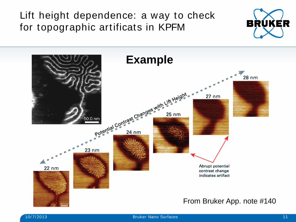
Lift height dependence: a way to check for topographic artificats in KPFM
10/7/2013 11 Bruker Nano Surfaces
Example
From Bruker App. note #140

Proof of real contrast: evolution of PF-KPFM resolution w/ lift height
10/7/2013 12 Bruker Nano Surfaces
50nm 40nm 28nm 75nm
No sudden loss of resolution = contrast not due to tip sticking
1um
Lift Height

Let’s zoom in on an interesting region..
10/7/2013 13 Bruker Nano Surfaces
0nm
14.5nm 1um
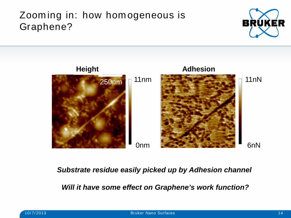
Zooming in: how homogeneous is Graphene?
Bruker Nano Surfaces
Height
0nm
11nm Adhesion
6nN
11nN
Substrate residue easily picked up by Adhesion channel
Will it have some effect on Graphene’s work function?
250nm
10/7/2013 14
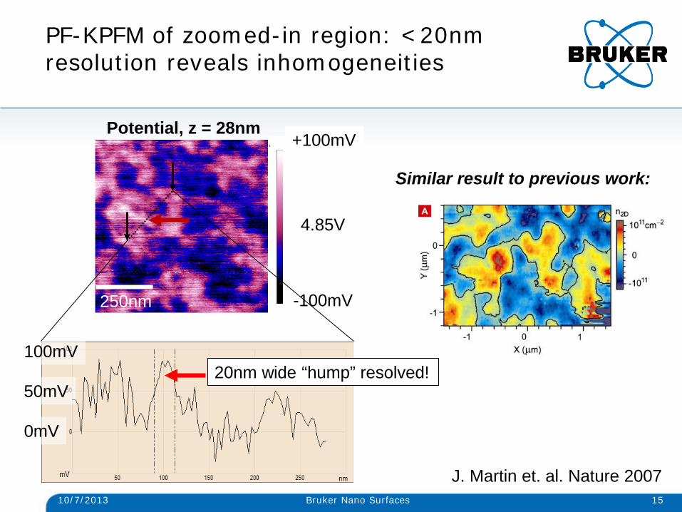
PF-KPFM of zoomed-in region: <20nm resolution reveals inhomogeneities
10/7/2013 15 Bruker Nano Surfaces
15
Potential, z = 28nm
250nm -100mV
+100mV
0mV
100mV
50mV
Similar result to previous work:
J. Martin et. al. Nature 2007
20nm wide “hump” resolved!
4.85V
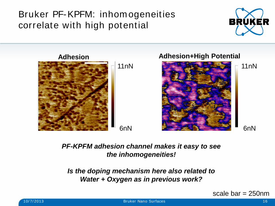
Bruker PF-KPFM: inhomogeneities correlate with high potential
10/7/2013 16 Bruker Nano Surfaces
Adhesion
6nN
11nN Adhesion+High Potential
6nN
11nN
PF-KPFM adhesion channel makes it easy to see the inhomogeneities!
Is the doping mechanism here also related to
Water + Oxygen as in previous work?
scale bar = 250nm

What is the effect of the environment on Graphene doping?
• Water? • Oxygen? • Is it reversible?
An environmentally controlled measurement is needed..
Cryogenic UHV KPFM would be great, but difficult/costly
Is there an easier way to study Graphene in a H2O+O2 free environment?
10/7/2013 Bruker Nano Surfaces 17

Unique Bruker technology: Glovebox Integrated System
Antechamber for introducing samples, pressure below 1E-6mbar
Argon Atmosphere, <1ppm H2O, 1ppm O2
10/7/2013 Bruker Nano Surfaces 18

Physical picture: what we expect to happen
10/7/2013 19 Bruker Nano Surfaces
Ambient GloveBox
𝐸F
Graphene is hole doped by Water and Oxygen
Water and Oxygen removed, Graphene nearly intrinsic
Potential for studying nearly-intrinsic Graphene without
Cryogenics or UHV
𝐸F
𝑊0gr 𝑊smp
𝑊𝑎
𝑊elec 𝑆∆𝑉𝑉𝐾𝑉
𝑊tip
Vacuum level

Physical picture confirmed: PF-KPFM in GloveBox shows lower contrast
10/7/2013 20 Bruker Nano Surfaces
Ambient GloveBox
Contrast between Graphene and SiN greatly reduced
Spatial inhomogeneities in Graphene also reduced
-200mV
500mV
-150mV
150mV

Physical picture confirmed: PF-KPFM in GloveBox shows lower contrast
10/7/2013 21 Bruker Nano Surfaces
Ambient GloveBox (same scale)
-200mV
500mV
-200mV
500mV
Graphene signal is nearly that of an insulator

Inhomogeneities greatly reduced in Glovebox
10/7/2013 22 Bruker Nano Surfaces
Potential
Glovebox
AFM
Air
250nm
-100mV
+100mV
-100mV
+100mV
4.85V ~4.6V

Another sample: larger KPFM scan
10/7/2013 23 Bruker Nano Surfaces
SiN Graphene
Au
Au
Graphene SiN
250 - 470mV 93mV
Three vastly different potentials for Graphene?
Potential in Air

KPFM Potential, in Glovebox before vacuum
SiN Graphene
Au
KPFM Potential, in Glovebox after vacuum
10/7/2013 Bruker Nano Surfaces 24
Au
Graphene SiN/chuck
284mV 193mV
334mV 133mV
Glovebox environment reduced Graphene workfunction by ~100mV
Wg ~ 4.7eV near Au contact, smaller farther away

Conclusion
• PF-KPFM’s spatial resolution is great: 20nm resolution images are achievable on Graphene
• PF-KPFM is sensitive: ~10meV sensitivity allows to easily distinguish inhomogeneities
• Glovebox Integrated System is a convenient promising environment for reducing Graphene’s work function to nearly intrinsic levels.
10/7/2013 25 Bruker Nano Surfaces

Backup slides
10/7/2013 26 Bruker Nano Surfaces

Tip Cone Contribution in KPFM FM gradient detection isolates contribution from tip
• FM-KPFM:
• The foremost 0.3% of the tip cone accounts for half of the signal in.
• FM can achieve a lateral resolution better than 50nm.
• AM-KPFM
• The contribution from the tip cone never reaches 50%.
• Its lateral resolution is dictated by the um-scale lever.
10/7/2013 27
0%
10%
20%
30%
40%
50%
60%
70%
80%
90%
100%
0% 0% 1% 10% 100%
Cone
Con
trib
utio
n%
Height Inclusion (h/H)%
FM z=10 nm FM z=50 nm
AM z=10 nm
AM z=50 nm
Based on SCM-PIT Geometry: W=30um, L=225um, H=10um, Cone Angle=45
Bruker Nano Surfaces