A Novel Low power and Area Efficient Carry-Lookahead Adder ...carry. This limitation is overcome by...
6
International Journal of Science and Research (IJSR) ISSN (Online): 2319-7064 Index Copernicus Value (2013): 6.14 | Impact Factor (2013): 4.438 Volume 4 Issue 5, May 2015 www.ijsr.net Licensed Under Creative Commons Attribution CC BY A Novel Low power and Area Efficient Carry- Lookahead Adder Using MOD-GDI Technique Pinninti Kishore 1 , P. V. Sridevi 2 , K. Babulu 3 , K.S Pradeep Chandra 4 1 Assistant Professor, Dept. of ECE, VNRVJIET, Hyderabad 2 Professor, Dept. of ECE, Andhra University College of Engg., Visakhapatnam 3 Professor, Dept. of ECE, JNTU College of Engg., Kakinada. 4 M.Tech(VLSI),Student, ECE Dept , VNRVJIET, Hyderabad. Abstract: Adders are given a fundamental importance in a wide variety of digital systems. Many improvements have been made to reduce the architectures of adders. The proposed method aims on Modified Gate diffusion input (MOD-GDI) which is a low power technique to design any digital system. This technique has been adopted from (GDI) Gate Diffusion Input - low power digital circuit design technique. The Mod-GDI technique which allows in reducing delay, power consumption and area of digital circuits, while maintaining functionality of logic design. This paper presents the Performance comparisons on low power techniques of basic combinational logic functions and to state that the proposed Modified Gate Diffusion Input logic (Mod-GDI) to be more power-efficient than the CMOS logic design. This paper also presents a novel structure of Carry-Lookahead Adder (CLA) using the primitive gates which are designed by MOD-GDI technique. This technique can be used to reduce the number of transistors compared to conventional CLA design. The design of the 8-bit CLA is primarily introduced and then the 16-bit CLA is followed. The designs are simulated using Mentor Graphics tool with a supply voltage of 1.8V at 90nm Process technology. Keywords: Gate Diffusion Input (GDI), Mod-GDI, Low power, Primitive Logic Gates, Carry-Lookahead Adder (CLA ). 1. Introduction In the VLSI industry, the low power circuits both arithmetic and logic circuits have become very important .Due to the rapid increase in the usage of the portable electronic devices[1] and [2], the VLSI design efforts are mainly focused on low power circuits with high-speed computation. In various DSP processors, Adder circuits are the main building blocks of the Arithmetic unit. In such processors the certain parameters like power, area, delay time etc are to be considered. So the designers are forced to concentrate on meeting up the constraints like high speed , small area, high throughput and low power consumption. There are many design styles of adders. Although, the Ripple carry adder is the smallest in design among the various adders available. But the computational speed of the ripple carry adder is very slow. Carry-Lookahead and Carry-Select Adders [3] are very fast than compared to the ripple carry adder. To reduce the area and power of these such adders, different techniques were used. Some of them are Pseudo NMOS [4], Dynamic CMOS, Clocked CMOS logic, Domino logic [4], Pass transistor logic .Although these several techniques have been proposed to reduce the power consumption, there were some limitations like increase in area, delay time which are not suitable for low priced systems. This paper presents the primitive circuits in achieving the parameters like low power, with high speed computation and less transistor count by using MOD-GDI technique than compared to the conventionally designed circuits. These designs are then combined to form the CLA’s of 8-bit and 16-bit. This paper is organized as follows: Section 2 Reviews the base work. Section 3 Introduces implementation of carry Look ahead adder. Simulation and results are shown in Section 4, followed by the Conclusion in Section 5. 2. Modified Gate Diffusion Input (MOD-GDI) Modified Gate Diffusion Input (MOD-GDI) is a new technique of low power digital circuit design. This technique is adopted from the GDI technique [5]. The MOD-GDI technique is mainly used to reduce the power dissipation, propagation delay and transistor count of the digital circuits. Though all these parameters are achieved using the GDI technique, the MOD-GDI technique is proposed to overcome some of the major limitations of the GDI technique like difficulty in fabrication process and additional circuitry to give inputs to the GDI based circuits. By using this technique the combinational logic gates like OR,AND, Inverter and 2 X 1 MUX are designed using two transistors, whereas four transistor are used for OR & AND logics and for 2 X 1 MUX the transistor count is 14 using CMOS design. Hence the MOD-GDI technique is a useful technique to reduce the area and also for less power dissipation. Figure1 shows the basic MOD-GDI cell. The MOD-GDI cell is very similar to the basic GDI cell, both consists of 3 input terminals G, P and N. In GDI[6] both the substrates of the PMOS and NMOS are connected to the source where as in the MOD-GDI the substrate of PMOS is connected to VDD and substrate of the NMOS is connected to the GND. Paper ID: SUB154415 1205
Transcript of A Novel Low power and Area Efficient Carry-Lookahead Adder ...carry. This limitation is overcome by...
International Journal of Science and Research (IJSR) ISSN (Online): 2319-7064
Index Copernicus Value (2013): 6.14 | Impact Factor (2013): 4.438
Volume 4 Issue 5, May 2015
www.ijsr.net Licensed Under Creative Commons Attribution CC BY
A Novel Low power and Area Efficient Carry-
Lookahead Adder Using MOD-GDI Technique
Pinninti Kishore1, P. V. Sridevi
2, K. Babulu
3, K.S Pradeep Chandra
4
1Assistant Professor, Dept. of ECE, VNRVJIET, Hyderabad
2Professor, Dept. of ECE, Andhra University College of Engg., Visakhapatnam
3Professor, Dept. of ECE, JNTU College of Engg., Kakinada.
4M.Tech(VLSI),Student, ECE Dept , VNRVJIET, Hyderabad.
Abstract: Adders are given a fundamental importance in a wide variety of digital systems. Many improvements have been made to
reduce the architectures of adders. The proposed method aims on Modified Gate diffusion input (MOD-GDI) which is a low power
technique to design any digital system. This technique has been adopted from (GDI) Gate Diffusion Input - low power digital circuit
design technique. The Mod-GDI technique which allows in reducing delay, power consumption and area of digital circuits, while
maintaining functionality of logic design. This paper presents the Performance comparisons on low power techniques of basic
combinational logic functions and to state that the proposed Modified Gate Diffusion Input logic (Mod-GDI) to be more power-efficient
than the CMOS logic design. This paper also presents a novel structure of Carry-Lookahead Adder (CLA) using the primitive gates
which are designed by MOD-GDI technique. This technique can be used to reduce the number of transistors compared to conventional
CLA design. The design of the 8-bit CLA is primarily introduced and then the 16-bit CLA is followed. The designs are simulated using
Mentor Graphics tool with a supply voltage of 1.8V at 90nm Process technology.
Keywords: Gate Diffusion Input (GDI), Mod-GDI, Low power, Primitive Logic Gates, Carry-Lookahead Adder (CLA ).
1. Introduction
In the VLSI industry, the low power circuits both arithmetic
and logic circuits have become very important .Due to the
rapid increase in the usage of the portable electronic
devices[1] and [2], the VLSI design efforts are mainly
focused on low power circuits with high-speed computation.
In various DSP processors, Adder circuits are the main
building blocks of the Arithmetic unit. In such processors the
certain parameters like power, area, delay time etc are to be
considered. So the designers are forced to concentrate on
meeting up the constraints like high speed , small area, high
throughput and low power consumption. There are many
design styles of adders. Although, the Ripple carry adder is
the smallest in design among the various adders available.
But the computational speed of the ripple carry adder is very
slow. Carry-Lookahead and Carry-Select Adders [3] are very
fast than compared to the ripple carry adder.
To reduce the area and power of these such adders, different
techniques were used. Some of them are Pseudo NMOS [4],
Dynamic CMOS, Clocked CMOS logic, Domino logic [4],
Pass transistor logic .Although these several techniques have
been proposed to reduce the power consumption, there were
some limitations like increase in area, delay time which are
not suitable for low priced systems. This paper presents the
primitive circuits in achieving the parameters like low
power, with high speed computation and less transistor count
by using MOD-GDI technique than compared to the
conventionally designed circuits. These designs are then
combined to form the CLA’s of 8-bit and 16-bit.
This paper is organized as follows: Section 2 Reviews the
base work. Section 3 Introduces implementation of carry
Look ahead adder. Simulation and results are shown in
Section 4, followed by the Conclusion in Section 5.
2. Modified Gate Diffusion Input (MOD-GDI)
Modified Gate Diffusion Input (MOD-GDI) is a new
technique of low power digital circuit design. This technique
is adopted from the GDI technique [5]. The MOD-GDI
technique is mainly used to reduce the power dissipation,
propagation delay and transistor count of the digital circuits.
Though all these parameters are achieved using the GDI
technique, the MOD-GDI technique is proposed to overcome
some of the major limitations of the GDI technique like
difficulty in fabrication process and additional circuitry to
give inputs to the GDI based circuits. By using this technique
the combinational logic gates like OR,AND, Inverter and 2
X 1 MUX are designed using two transistors, whereas four
transistor are used for OR & AND logics and for 2 X 1 MUX
the transistor count is 14 using CMOS design. Hence the
MOD-GDI technique is a useful technique to reduce the area
and also for less power dissipation.
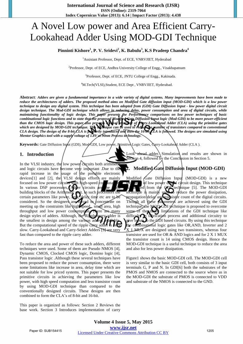
Figure1 shows the basic MOD-GDI cell. The MOD-GDI cell
is very similar to the basic GDI cell, both consists of 3 input
terminals G, P and N. In GDI[6] both the substrates of the
PMOS and NMOS are connected to the source where as in
the MOD-GDI the substrate of PMOS is connected to VDD
and substrate of the NMOS is connected to the GND.
Paper ID: SUB154415 1205
International Journal of Science and Research (IJSR) ISSN (Online): 2319-7064
Index Copernicus Value (2013): 6.14 | Impact Factor (2013): 4.438
Volume 4 Issue 5, May 2015
www.ijsr.net Licensed Under Creative Commons Attribution CC BY
Figure 1: The basic Mod-GDI cell
Table 1: Input configurations for different logic functions N NS P PS G D Function
0 0 1 1 A Al INVETER
B 0 0 1 A AB AND
A 0 B 1 A A+B OR
Al 0 A 1 B AlB+ABl EX-OR(basic)
A 0 Al 1 B AB+AlBl EX-NOR(basic)
0 0 B B A AlB FUNCTION
C 0 B 1 A AlB+AC MUX
Table 1, shows the input configuration of the different
functions which are obtained by the basic MOD-GDI cell.
The inverter input configuration is same for both the CMOS
and MOD-GDI technique, so there will be no difference in
the power dissipation. The remaining functions vary in
configuration. The input configuration of the EX-OR and
EX-NOR [7] as given in the table are the basic configuration.
In order to get more output swing the configurations were
modified to achieve better computation. The proposed EX-
OR and EX-NOR gates can be seen in Figure 7and Figure 8.
Table II shows the comparison between four styles [5][8] in
terms of transistor count.
Table 2: Comparison of Transistor Count Functions Mod-GDI DPL TG CMOS
AND 2 7 6 6
OR 2 7 6 6
XOR 4 8 8 12
XNOR 4 8 8 12
2.1 Proposed Primitive Gates using MOD-GDI technique
Figure 2 – Figure 9 represents the proposed designs of
primitive gates namely Inverter, 2 input AND gate, 2 input
OR gate, 2 input NAND gate, 2 input NOR gate, 2 input
EX-OR gate, 2 input EX-NOR gate and 2X1 multiplexer
using Modified GDI technique. All the proposed designs are
design at 90nm technology with very low supply voltage of
1.8V and to get minimum area the designs are designed.
2.1.1. Inverter
Figure 2: Inverter using Mod-GDI Technique
2.1.2. Two input AND gate
Figure 3: Two input AND gate using Mod-GDI Technique
2.1.3. Two input OR gate
Figure 4: Two input OR gate using Mod-GDI Technique
2.1.4. Two input NAND gate
Figure 5: Two input NAND gate using Mod-GDI Technique
Paper ID: SUB154415 1206
International Journal of Science and Research (IJSR) ISSN (Online): 2319-7064
Index Copernicus Value (2013): 6.14 | Impact Factor (2013): 4.438
Volume 4 Issue 5, May 2015
www.ijsr.net Licensed Under Creative Commons Attribution CC BY
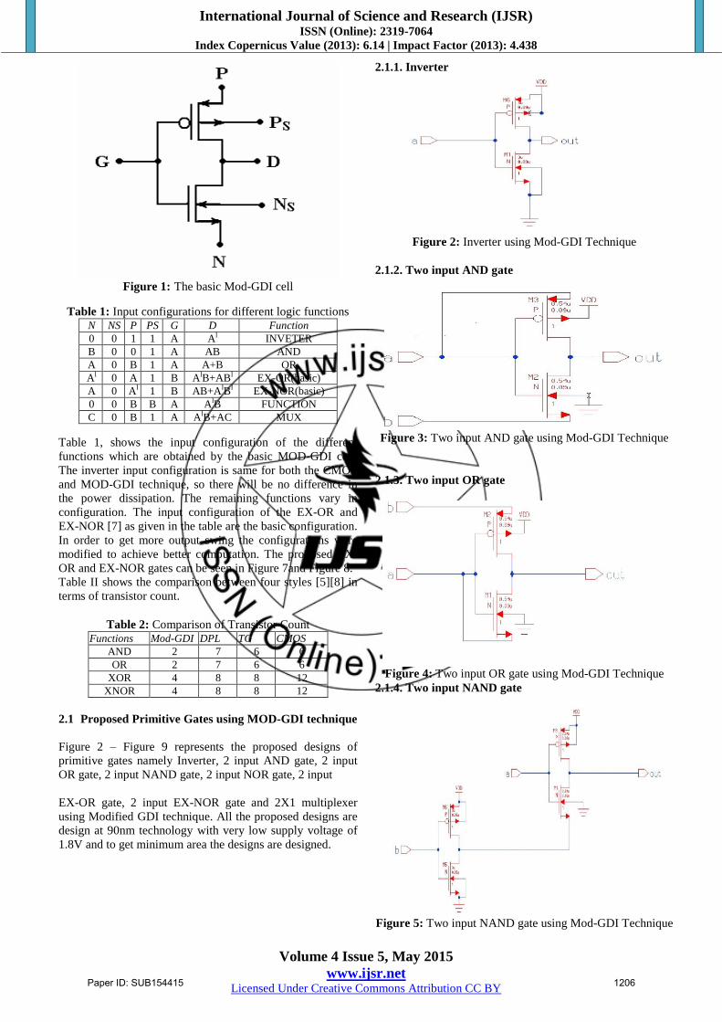
2.1.5. Two input NOR gate
Figure 6: Two input NOR gate using Mod-GDI Technique
2.1.6. Two input EX-OR gate
Figure 7: Two input EX-OR gate using Mod-GDI
Technique
2.1.7. Two input EX-NOR gate
Figure 8: Two input EX-NOR gate using Mod-GDI
Technique
2.1.8. 2 X 1 Multiplexer
Figure 9: 2 x 1 MUX using Mod-GDI Technique
Table 3 shows the comparison of power dissipations among
three different design techniques. These proposed designs are
operated at a low voltage of 1.8V. The proposed designs are
simulated at 90nm technology. From the table it is observed
that total power dissipation of Mod-GDI designs is very low
comparative to all other methods.
These readings of power dissipation were obtained by
implementing the gates in the CMOS[9], GDI and MOD-
GDI techniques in the Mentor Graphics Pyxis schematic
tool.
Table 3: Comparison of total power dissipation with
respective to all other techniques Primitive Gates Total power dissipation
CMOS GDI MOD-GDI
INVERTER 8.2774 pw 8.2774 pw 8.2774 pw
AND 39.6428 uw 40.3738 nw 6.5160 pw
OR 44.0824 uw 40.3738 nw 6.5160 pw
NAND 0.1641 uw 48.5046 pw 14.7934 pw
NOR 1.9706 uw 48.5046 pw 14.7934 pw
XOR 85.1884 uw 96.6106 nw 13.0320 pw
XNOR 85.7694 uw 49.9776 nw 21.3099 pw
2X1 MUX 42.7019 uw 37.7952 nw 6.5160 pw
Table 3 clearly shows that ,using MOD-GDI technique the
total power dissipation has decreased drastically when
compared with CMOS and GDI techniques. Not only the
power dissipation but also the transistor count was also
decreased resulting the optimized and area efficient
combinational logic designs were obtained .
3. Proposed Carry-Lookahead Adder (CLA)
When we discuss about adders, the Ripple carry adders are
the basic adders which comes to count. The limiting factor of
the Ripple carry adder is the time taken to propagate the
carry. This limitation is overcome by the carry Lookahead
adder by calculating the carry in advance, according to the
input values given to the adder. Thus it results in reducing
the propagation time of the carry. To understand how the
carry look ahead adder[10] works, let us manipulate the
Boolean expression dealing with the full adder.
Paper ID: SUB154415 1207
International Journal of Science and Research (IJSR) ISSN (Online): 2319-7064
Index Copernicus Value (2013): 6.14 | Impact Factor (2013): 4.438
Volume 4 Issue 5, May 2015
www.ijsr.net Licensed Under Creative Commons Attribution CC BY
In a full adder the propagate P and generate G is given as:
Pi = Ai ⊕ Bi (1)
Gi = Ai . Bi (2)
Equations (1) and (2) gives carry propagate and carry
generate respectively.Note that both propagate and the
generate signals will depend on the input bits given and will
be valid only after one gate delay.
The final expressions for the Output sum and carryout are
given by:
Si = Pi ⊕ Ci-1 (3)
Ci+1= Gi + Pi*Ci (4)
These equations show that carry signal will be generated
only in two cases:
1. If both bits Ai and Bi are 1
2. If either Ai or Bi is 1 and the carry-in Ci is 1.
3.1 Design of Carry look ahead adder
Let us now apply these equations to design carry look ahead
adder of 8-bit initially and then followed by 16-bit. By using
the primitive gates i.e. AND,OR and EX-OR gates we can
design the CLA. For the 8-bit CLA we need the all 8-bit
circuits of AND, OR and EX-OR. There are three stages to
implement the CLA. In the first stage entering the input
value of Ai and Bi in binary form. It also consists XOR gate
(with input Bi and Cin) .The second stage is to generate Pi
and Gi signals. It consists of AND gates and XOR gates. The
output signals from this level are P’s and G’s signals. In the
third stage the generation of Ci signals as defined in
expression (4). The output signals Ci come from OR ing Gi
and the outcome from AND ing Ci-1 and Pi. This level
consists of OR and AND gate. In the fourth stage , the
generation of the sum signals Si. XOR gates are valid in this
level and the output value is shown in binary form at the
output. Thus we obtain the design of the 8-bit carry
Lookahead adder as shown in the Figure 10.
3.1.1. 8- bit Carry Lookahead Adder
Figure 10: 8- Bit Carry Lookahead Adder using Mod-GDI
Technique
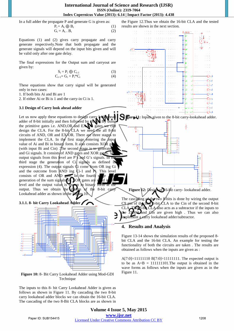
The inputs to this 8- bit Carry Lookahead Adder is given as
follows as shown in Figure 11. By cascading the two 8-bit
carry lookahead adder blocks we can obtain the 16-bit CLA.
The cascading of the two 8-Bit CLA blocks are as shown in
the Figure 12.Thus we obtain the 16-bit CLA and the tested
results are shown in the next section.
Figure 11: Inputs given to the 8-bit carry-lookahead adder.
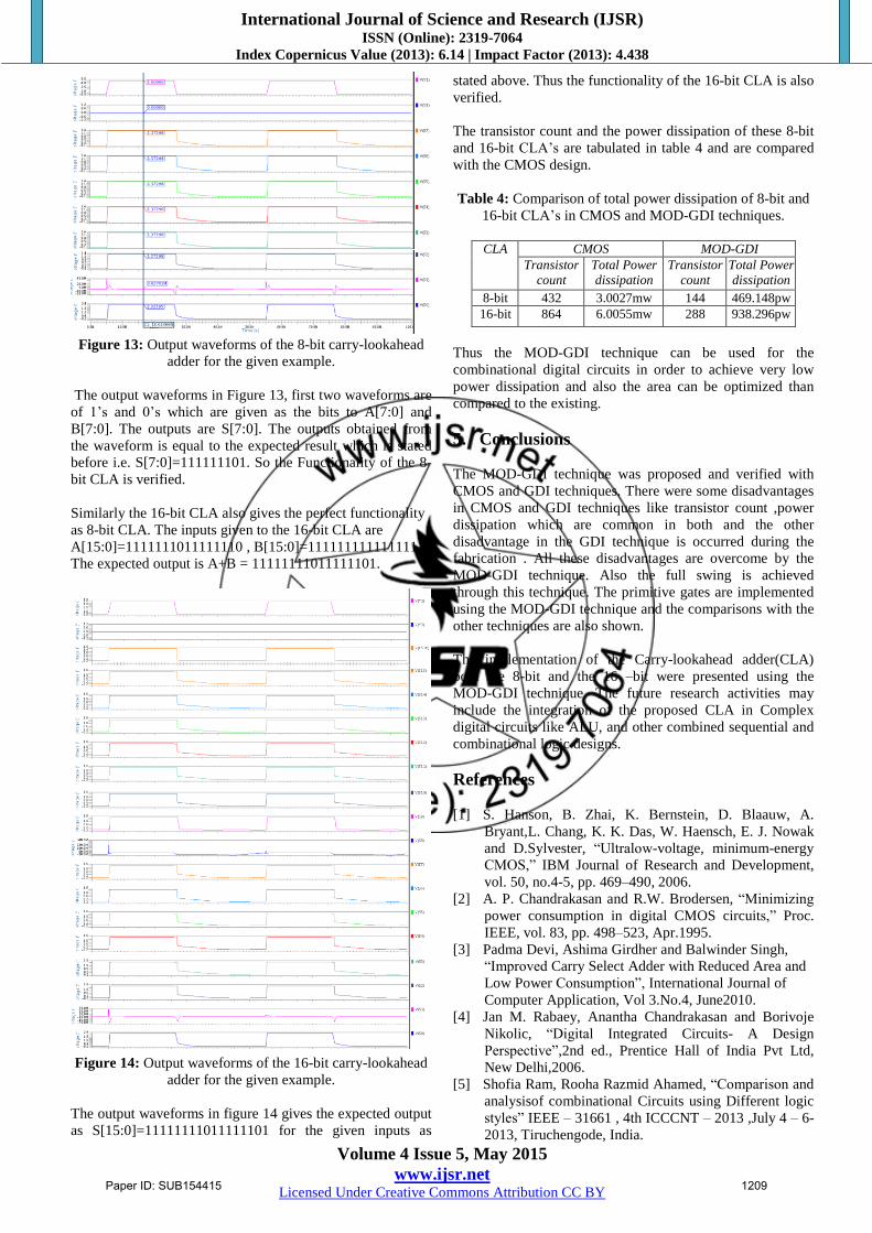
Figure 12: Design of 16-bit carry- lookahead adder.
The cascading of the two 8-bits is done by wiring the output
C9 pin of the first 8-bit CLA to the Cin of the second 8-bit
CLA. This 8-bit CLA also acts as a subtractor if the inputs to
the ZERO and Cin are given high . Thus we can also
implement a carry lookahead adder/subtractor.
4. Results and Analysis Figure 13-14 shows the simulation results of the proposed 8-
bit CLA and the 16-bit CLA. An example for testing the
functionality of both the circuits are taken . The results are
obtained as follows when the inputs are given as :
A[7:0]=11111110 B[7:0]=11111111. The expected output is
to be as A+B = 111111101.The output is obtained in the
wave forms as follows when the inputs are given as in the
Figure 11.
Paper ID: SUB154415 1208
International Journal of Science and Research (IJSR) ISSN (Online): 2319-7064
Index Copernicus Value (2013): 6.14 | Impact Factor (2013): 4.438
Volume 4 Issue 5, May 2015
www.ijsr.net Licensed Under Creative Commons Attribution CC BY
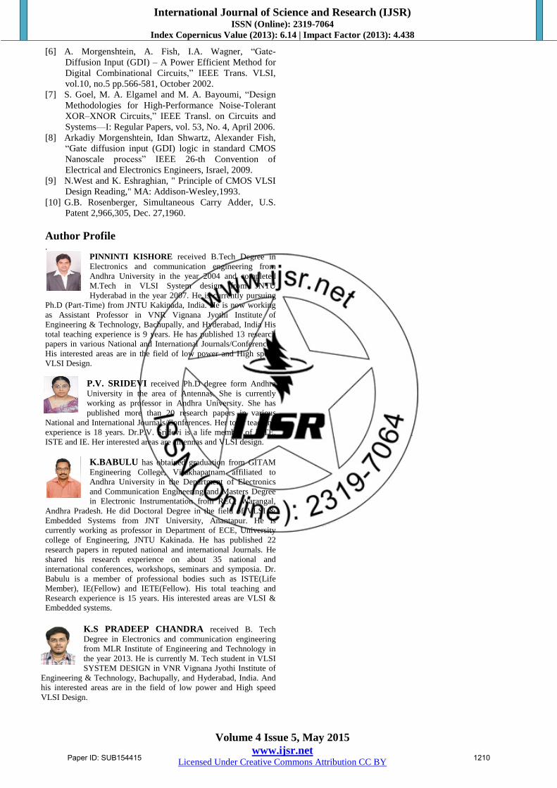
Figure 13: Output waveforms of the 8-bit carry-lookahead
adder for the given example.
The output waveforms in Figure 13, first two waveforms are
of 1’s and 0’s which are given as the bits to A[7:0] and
B[7:0]. The outputs are S[7:0]. The outputs obtained from
the waveform is equal to the expected result which is stated
before i.e. S[7:0]=111111101. So the Functionality of the 8-
bit CLA is verified.
Similarly the 16-bit CLA also gives the perfect functionality
as 8-bit CLA. The inputs given to the 16-bit CLA are
A[15:0]=1111111011111110 , B[15:0]=1111111111111111
The expected output is A+B = 11111111011111101.
Figure 14: Output waveforms of the 16-bit carry-lookahead
adder for the given example.
The output waveforms in figure 14 gives the expected output
as S[15:0]=11111111011111101 for the given inputs as
stated above. Thus the functionality of the 16-bit CLA is also
verified.
The transistor count and the power dissipation of these 8-bit
and 16-bit CLA’s are tabulated in table 4 and are compared
with the CMOS design.
Table 4: Comparison of total power dissipation of 8-bit and
16-bit CLA’s in CMOS and MOD-GDI techniques.
CLA CMOS MOD-GDI
Transistor
count
Total Power
dissipation
Transistor
count
Total Power
dissipation
8-bit 432 3.0027mw 144 469.148pw
16-bit 864 6.0055mw 288 938.296pw
Thus the MOD-GDI technique can be used for the
combinational digital circuits in order to achieve very low
power dissipation and also the area can be optimized than
compared to the existing.
5. Conclusions
The MOD-GDI technique was proposed and verified with
CMOS and GDI techniques. There were some disadvantages
in CMOS and GDI techniques like transistor count ,power
dissipation which are common in both and the other
disadvantage in the GDI technique is occurred during the
fabrication . All these disadvantages are overcome by the
MOD-GDI technique. Also the full swing is achieved
through this technique. The primitive gates are implemented
using the MOD-GDI technique and the comparisons with the
other techniques are also shown.
The implementation of the Carry-lookahead adder(CLA)
both the 8-bit and the 16 –bit were presented using the
MOD-GDI technique. The future research activities may
include the integration of the proposed CLA in Complex
digital circuits like ALU, and other combined sequential and
combinational logic designs.
References
[1] S. Hanson, B. Zhai, K. Bernstein, D. Blaauw, A.
Bryant,L. Chang, K. K. Das, W. Haensch, E. J. Nowak
and D.Sylvester, ―Ultralow-voltage, minimum-energy
CMOS,‖ IBM Journal of Research and Development,
vol. 50, no.4-5, pp. 469–490, 2006.
[2] A. P. Chandrakasan and R.W. Brodersen, ―Minimizing
power consumption in digital CMOS circuits,‖ Proc.
IEEE, vol. 83, pp. 498–523, Apr.1995.
[3] Padma Devi, Ashima Girdher and Balwinder Singh,
―Improved Carry Select Adder with Reduced Area and
Low Power Consumption‖, International Journal of
Computer Application, Vol 3.No.4, June2010.
[4] Jan M. Rabaey, Anantha Chandrakasan and Borivoje
Nikolic, ―Digital Integrated Circuits- A Design
Perspective‖,2nd ed., Prentice Hall of India Pvt Ltd,
New Delhi,2006.
[5] Shofia Ram, Rooha Razmid Ahamed, ―Comparison and
analysisof combinational Circuits using Different logic
styles‖ IEEE – 31661 , 4th ICCCNT – 2013 ,July 4 – 6-
2013, Tiruchengode, India.
Paper ID: SUB154415 1209
International Journal of Science and Research (IJSR) ISSN (Online): 2319-7064
Index Copernicus Value (2013): 6.14 | Impact Factor (2013): 4.438
Volume 4 Issue 5, May 2015
www.ijsr.net Licensed Under Creative Commons Attribution CC BY
[6] A. Morgenshtein, A. Fish, I.A. Wagner, ―Gate-
Diffusion Input (GDI) – A Power Efficient Method for
Digital Combinational Circuits,‖ IEEE Trans. VLSI,
vol.10, no.5 pp.566-581, October 2002.
[7] S. Goel, M. A. Elgamel and M. A. Bayoumi, ―Design
Methodologies for High-Performance Noise-Tolerant
XOR–XNOR Circuits,‖ IEEE Transl. on Circuits and
Systems—I: Regular Papers, vol. 53, No. 4, April 2006.
[8] Arkadiy Morgenshtein, Idan Shwartz, Alexander Fish,
―Gate diffusion input (GDI) logic in standard CMOS
Nanoscale process‖ IEEE 26-th Convention of
Electrical and Electronics Engineers, Israel, 2009.
[9] N.West and K. Eshraghian, " Principle of CMOS VLSI
Design Reading," MA: Addison-Wesley,1993.
[10] G.B. Rosenberger, Simultaneous Carry Adder, U.S.
Patent 2,966,305, Dec. 27,1960.
Author Profile .
PINNINTI KISHORE received B.Tech Degree in
Electronics and communication engineering from
Andhra University in the year 2004 and completed
M.Tech in VLSI System design from JNTU
Hyderabad in the year 2007. He is currently pursuing
Ph.D (Part-Time) from JNTU Kakinada, India. He is now working
as Assistant Professor in VNR Vignana Jyothi Institute of
Engineering & Technology, Bachupally, and Hyderabad, India His
total teaching experience is 9 years. He has published 13 research
papers in various National and International Journals/Conferences.
His interested areas are in the field of low power and High speed
VLSI Design.
P.V. SRIDEVI received Ph.D degree form Andhra
University in the area of Antennas. She is currently
working as professor in Andhra University. She has
published more than 20 research papers in various
National and International Journals/Conferences. Her total teaching
experience is 18 years. Dr.P.V. Sridevi is a life member of IETE,
ISTE and IE. Her interested areas are antennas and VLSI design.
K.BABULU has obtained graduation from GITAM
Engineering College, Visakhapatnam affiliated to
Andhra University in the Department of Electronics
and Communication Engineering and Masters Degree
in Electronic Instrumentation from REC, Warangal,
Andhra Pradesh. He did Doctoral Degree in the field of VLSI &
Embedded Systems from JNT University, Anantapur. He is
currently working as professor in Department of ECE, University
college of Engineering, JNTU Kakinada. He has published 22
research papers in reputed national and international Journals. He
shared his research experience on about 35 national and
international conferences, workshops, seminars and symposia. Dr.
Babulu is a member of professional bodies such as ISTE(Life
Member), IE(Fellow) and IETE(Fellow). His total teaching and
Research experience is 15 years. His interested areas are VLSI &
Embedded systems.
K.S PRADEEP CHANDRA received B. Tech
Degree in Electronics and communication engineering
from MLR Institute of Engineering and Technology in
the year 2013. He is currently M. Tech student in VLSI
SYSTEM DESIGN in VNR Vignana Jyothi Institute of
Engineering & Technology, Bachupally, and Hyderabad, India. And
his interested areas are in the field of low power and High speed
VLSI Design.
Paper ID: SUB154415 1210


![Arithmetic Circuits 3 - KFUPM · Presentation Outline Carry Lookahead Adder BCD Adder Binary Multiplier Carry-Save Adders in Multipliers. ... BCD Adder 4 A [3:0] 4 B [3:0] C out C](https://static.fdocuments.us/doc/165x107/5f4e251bbf3d40066f1e07a0/arithmetic-circuits-3-kfupm-presentation-outline-carry-lookahead-adder-bcd-adder.jpg)