A novel Al Ga As/In Ga As/GaAs quantum well Hall...
5
Semiconductor Physics, Quantum Electronics & Optoelectronics, 2012. V. 15, N 1. P. 72-76. © 2012, V. Lashkaryov Institute of Semiconductor Physics, National Academy of Sciences of Ukraine 72 PACS 53.50.Td, 71.76, 72.80.Ey, 85.30.De, 85.30.Fg A novel Al 0.33 Ga 0.67 As/In 0.15 Ga 0.85 As/GaAs quantum well Hall device grown on (111) GaAs H. Sghaier, L. Bouzaiene, L. Sfaxi, H. Maaref Laboratoire de Micro-Optoélectronique et nanostructures de Monastir Faculté des Sciences de Monastir, Avenue de l’Environnement, 5000 Monastir (Tunisia) Institut Supérieur d’Informatique et de Mathématiques de Monastir, Avenue de la corniche, Monastir Abstract. In this study, we look at the advantages of (111) GaAs substrate over (001) one, when used to grow Hall devices by MBE. In top of that, we explore the consequence of a modified design of modulation doping pseudomorphic AlGaAs/InGaAs/GaAs, and we suggest a new quantum well structure for a Hall device grown on (111) GaAs substrate, with the objective of improving its performances. From self-consistent calculations, we find that the electron concentration n s in the interface region is enhanced. This implies that one can have a wider spacer layer and still have the same n s with the result that the mobility is improved. This result should be valuable for many types of devices. We specifically consider Hall sensors, where it is desirable to have a low electron concentration and high mobility. Keywords: quantum well, Hall device, electron concentration. Manuscript received 19.01.11; revised version received 29.12.11; accepted for publication 26.01.12; published online 29.03.12. 1. Introduction Semiconductor magnetic field sensors such as Hall devices are widely used in many industrial and domestic applications. In recent years, Hall sensors using modulation-doped AlGaAs/InGaAs have been proposed [1-3]. Hall devices based on pseudomorphic heterostructures have attracted increasing interest recently by virtue of their high electron mobility combined with moderate sheet carrier densities, low temperature dependence of the output Hall voltage and large signal-to-noise ratios [4]. The AlGaAs/InGaAs system deserves special attention in this respect. It is the system of choice in the design of high-speed devices and RF circuits. Modulation-doped hetero- structures with a high electron mobility and low electron concentration can be used to achieve very high magnetic sensitivities [5]. Hall effect devices are by far the most widely used magnetic sensors today. Their future mainly depends on whether means will be developed to enhance their sensitivity and their temperature stability [6]. The key parameters for such devices which determine their sensitivity to magnetic field are their high electron mobility and low electron density. In a previous study, we have investigated the effect of piezoelectric field built in AlGaAs/InGaAs/GaAs pseudomorphic HEMT grown on (111)A substrate, and we have found that both electron density and mobility are enhanced [7]. In this paper, we combine results determined both in [6] and [7], and we report the design of a new two-dimensional electron gas Hall device based on AlGaAs/InGaAs/GaAs heterostructure, which was particularly optimized for low magnetic field measurements. Charge density profiles, total 2D electron densities, and sensitivities are calculated from coupled Schrödinger and Poisson equations. The main idea is to substitute a (111)A GaAs substrate to (001) one and to increase the mobility without decreasing the carrier concentration by means of special doping profile. Instead of having a -doped layer in a homogenous Al x Ga 1-x As barrier material, we consider the possibility to have the donors in a narrow quantum well embedded in the barrier with a lower aluminum concentration than the rest of the barrier.
Transcript of A novel Al Ga As/In Ga As/GaAs quantum well Hall...

Semiconductor Physics, Quantum Electronics & Optoelectronics, 2012. V. 15, N 1. P. 72-76.
© 2012, V. Lashkaryov Institute of Semiconductor Physics, National Academy of Sciences of Ukraine
72
PACS 53.50.Td, 71.76, 72.80.Ey, 85.30.De, 85.30.Fg
A novel Al0.33Ga0.67As/In0.15Ga0.85As/GaAs quantum well Hall device grown on (111) GaAs
H. Sghaier, L. Bouzaiene, L. Sfaxi, H. MaarefLaboratoire de Micro-Optoélectronique et nanostructures de Monastir Faculté des Sciences de Monastir, Avenue de l’Environnement, 5000 Monastir (Tunisia) Institut Supérieur d’Informatique et de Mathématiques de Monastir, Avenue de la corniche, Monastir
Abstract. In this study, we look at the advantages of (111) GaAs substrate over (001) one, when used to grow Hall devices by MBE. In top of that, we explore the consequence of a modified design of modulation doping pseudomorphic AlGaAs/InGaAs/GaAs, and we suggest a new quantum well structure for a Hall device grown on (111) GaAs substrate, with the objective of improving its performances. From self-consistent calculations, we find that the electron concentration ns in the interface region is enhanced. This implies that one can have a wider spacer layer and still have the same ns
with the result that the mobility is improved. This result should be valuable for many types of devices. We specifically consider Hall sensors, where it is desirable to have a low electron concentration and high mobility.
Keywords: quantum well, Hall device, electron concentration.
Manuscript received 19.01.11; revised version received 29.12.11; accepted for publication 26.01.12; published online 29.03.12.
1. Introduction
Semiconductor magnetic field sensors such as Hall devices are widely used in many industrial and domestic applications. In recent years, Hall sensors using modulation-doped AlGaAs/InGaAs have been proposed [1-3]. Hall devices based on pseudomorphic heterostructures have attracted increasing interest recently by virtue of their high electron mobility combined with moderate sheet carrier densities, low temperature dependence of the output Hall voltage and large signal-to-noise ratios [4]. The AlGaAs/InGaAs system deserves special attention in this respect. It is the system of choice in the design of high-speed devices and RF circuits. Modulation-doped hetero-structures with a high electron mobility and low electron concentration can be used to achieve very high magnetic sensitivities [5].
Hall effect devices are by far the most widely used magnetic sensors today. Their future mainly depends on whether means will be developed to enhance their sensitivity and their temperature stability [6]. The key
parameters for such devices which determine their sensitivity to magnetic field are their high electron mobility and low electron density. In a previous study, we have investigated the effect of piezoelectric field built in AlGaAs/InGaAs/GaAs pseudomorphic HEMT grown on (111)A substrate, and we have found that both electron density and mobility are enhanced [7]. In this paper, we combine results determined both in [6] and [7], and we report the design of a new two-dimensional electron gas Hall device based on AlGaAs/InGaAs/GaAs heterostructure, which was particularly optimized for low magnetic field measurements. Charge density profiles, total 2D electron densities, and sensitivities are calculated from coupled Schrödinger and Poisson equations. The main idea is to substitute a (111)A GaAs substrate to (001) one and to increase the mobility without decreasing the carrier concentration by means of special doping profile. Instead of having a -doped layer in a homogenous AlxGa1-xAs barrier material, we consider the possibility to have the donors in a narrow quantum well embedded in the barrier with a lower aluminum concentration than the rest of the barrier.
Semiconductor Physics, Quantum Electronics & Optoelectronics, 2012. V. 15, N 1. P. 72-76.
© 2012, V. Lashkaryov Institute of Semiconductor Physics, National Academy of Sciences of Ukraine
73
2. Device structure
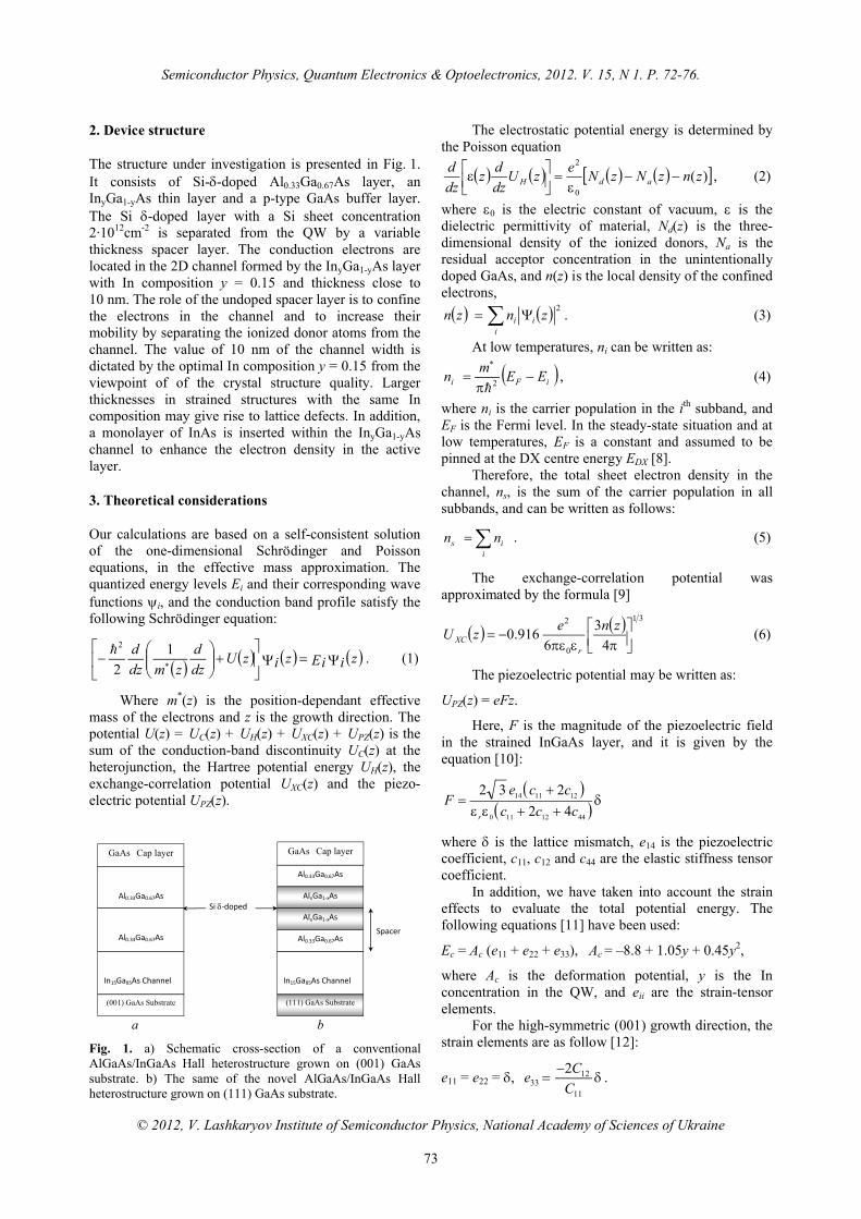
The structure under investigation is presented in Fig. 1. It consists of Si--doped Al0.33Ga0.67As layer, an InyGa1-yAs thin layer and a p-type GaAs buffer layer.The Si -doped layer with a Si sheet concentration 2∙1012cm-2 is separated from the QW by a variable thickness spacer layer. The conduction electrons are located in the 2D channel formed by the InyGa1-yAs layer with In composition y = 0.15 and thickness close to10 nm. The role of the undoped spacer layer is to confine the electrons in the channel and to increase their mobility by separating the ionized donor atoms from the channel. The value of 10 nm of the channel width is dictated by the optimal In composition y = 0.15 from the viewpoint of of the crystal structure quality. Larger thicknesses in strained structures with the same In composition may give rise to lattice defects. In addition, a monolayer of InAs is inserted within the InyGa1-yAs channel to enhance the electron density in the active layer.
3. Theoretical considerations
Our calculations are based on a self-consistent solution of the one-dimensional Schrödinger and Poisson equations, in the effective mass approximation. The quantized energy levels Ei and their corresponding wave functions i, and the conduction band profile satisfy the following Schrödinger equation:
ziEizizUdz
d
zmdz
d
1
2
2. (1)
Where m*(z) is the position-dependant effective mass of the electrons and z is the growth direction. The potential U(z) = UC(z) + UH(z) + UXC(z) + UPZ(z) is the sum of the conduction-band discontinuity UC(z) at the heterojunction, the Hartree potential energy UH(z), the exchange-correlation potential UXC(z) and the piezo-electric potential UPZ(z).
GaAs Cap layer
Al0.33Ga0.67As
In15Ga85As Channel
(001) GaAs Substrate
Al0.33Ga0.67As
Al0.33Ga0.67As
AlxGa1-xAs
AlxGa1-xAs
(111) GaAs Substrate
Al0.33Ga0.67As
Si -doped
Spacer
GaAs Cap layer
In15Ga85As Channel
a b
Fig. 1. a) Schematic cross-section of a conventional AlGaAs/InGaAs Hall heterostructure grown on (001) GaAs substrate. b) The same of the novel AlGaAs/InGaAs Hall heterostructure grown on (111) GaAs substrate.
The electrostatic potential energy is determined by the Poisson equation
)(0
2
znzNzNe
zUdz
dz
dz
dadH
, (2)
where 0 is the electric constant of vacuum, is the dielectric permittivity of material, Nd(z) is the three-dimensional density of the ionized donors, Na is the residual acceptor concentration in the unintentionally doped GaAs, and n(z) is the local density of the confined electrons,
2znzn i
ii . (3)
At low temperatures, ni can be written as:
iFi EEm
n
2, (4)
where ni is the carrier population in the ith subband, and EF is the Fermi level. In the steady-state situation and at low temperatures, EF is a constant and assumed to be pinned at the DX centre energy EDX [8].
Therefore, the total sheet electron density in the channel, ns, is the sum of the carrier population in all subbands, and can be written as follows:
i
is nn . (5)
The exchange-correlation potential was approximated by the formula [9]
31
0
2
4
3
6916.0
znezU
rXC (6)
The piezoelectric potential may be written as:
UPZ(z) = eFz.
Here, F is the magnitude of the piezoelectric field in the strained InGaAs layer, and it is given by the equation [10]:
4412110
121114
42
232
ccc
cceF
r
where is the lattice mismatch, e14 is the piezoelectric coefficient, c11, c12 and c44 are the elastic stiffness tensor coefficient.
In addition, we have taken into account the strain effects to evaluate the total potential energy. The following equations [11] have been used:
Ec = Ac (e11 + e22 + e33), Ac = –8.8 + 1.05y + 0.45y2,
where Ac is the deformation potential, y is the In concentration in the QW, and eii are the strain-tensor elements.
For the high-symmetric (001) growth direction, the strain elements are as follow [12]:
e11 = e22 = ,
11
1233
2
C
Ce .

Semiconductor Physics, Quantum Electronics & Optoelectronics, 2012. V. 15, N 1. P. 72-76.
© 2012, V. Lashkaryov Institute of Semiconductor Physics, National Academy of Sciences of Ukraine
74
Fig. 2. Calculated band diagram for Hall structures: (a) conventional structure grown on (001) substrate with the spacer width 10 nm; (b) transitional structure grown on (111) substrate with the spacer width 10 nm; (c) transitional structure with the spacer width 21 nm; (d) novel structure (silicon in a quantum well) with the spacer width 21 nm, and the aluminum mole fraction 0.17. The lowest two subbands E0 and E1 are indicated together with the corresponding wave functions. E2
represents the calculated energy of the lowest bound state localized to the embedded Al0.15Ga0.85As layer. EDX represents the DX center energy. The Fermi level is represented by the dashed line.
For high-symmetric (111) growth direction, the strain elements are as follow [12]:
441211
44332211 42
4
ccc
ceee
with the lattice mismatch = (aGaAs – aInGaAs)/aInGaAs.The algorithm solves the one-dimensional
Schrödinger equation along a series of slices in the growth direction. Each slice corresponds to one monolayer. After the Schrödinger’s equation solution is taken, the carrier concentration calculated from Schrödinger’s equation is substituted into the charge part of the Poisson’s equation. The potential derived from the solution of Poisson’s equation is substituted back to Schrödinger’s equation. This solution process is continued until convergence is reached, and a self-consistent solution of Schrödinger’s and Poisson’s equation is obtained.
4. Results and discussions
The Hall voltage is given by
sH en
IBU , (7)
where I is the current, B – perpendicular magnetic field, e – the electronic charge, ns – sheet electron concentra-tion, and – geometric correction factor.
For a greek-cross structures where the length of active area is about one-third of the distance between contacts, 1 [13]. Thus,
UH EWB, (8)
where is the electron mobility, E – electric field in the active region of the Hall device, and W – width of the active region.
The latter relationship shows that the absolute sensitivity of the Hall device
WEdB
dUS H
A . (9)
Therefore, for high sensitivity devices, must be as high as possible.
On the other hand, the ratio of the absolute sensitivity to current is the current-related sensitivity,
endB
dU
IS
s
HI
11 . (10)
The smaller ns is, the higher SI is. Thus, for high sensitivity devices, ns must be as low as possible. However, this will lead to very high resistance devices, which will have a negative impact on noise performance.
In modulation-doped structures a two-dimensional electron gas is formed at the AlGaAs/InGaAs heterointerface due to the electron affinity difference between two materials. The electrons are separated from

Semiconductor Physics, Quantum Electronics & Optoelectronics, 2012. V. 15, N 1. P. 72-76.
© 2012, V. Lashkaryov Institute of Semiconductor Physics, National Academy of Sciences of Ukraine
75
Table. Electron density in the channel calculated for different aluminum mole fractions in the embedded QW in the barrier and for different spacer widths. The sample (a) represents the standard heterostructure grown on (001) substrate. The sample (d) grown on (111) substrate exhibits the same ns as the sample (a), but has a larger spacer width, leading to much higher device sensitivity without degradation in noise characteristics.
Sample a b c dSubstrate
orientation(001) (111) (111) (111)
Spacer thickness (nm)
10.0 10.0 21 21
Al mole fraction in the embedded
QW
0.33 0.33 0.33 0.17
ns (1012 cm-2) 1.05 1.29 0.73 1.05
the donors in the AlGaAs by a thin spacer layer, which decreases the impurity scattering, and enhances the electron mobility [14]. In theory, a higher value of the electron mobility can be obtained by increasing the spacer layer thickness. The spacer layer thickness controls the amount of charge trapped in the quantum well (QW), ns and hence the current-related sensitivity (SI). However, the cost of such improvement is a drastic loss of electron concentration in the channel, leading to a very high resistive device.
In a previous studies [15], we have shown that the charge density may be enhanced by introducing Si -doping in a thin AlxGa1-xAs QW embedded in the Al0.33Ga0.67As barrier with x smaller than 0.33. We have observed an enhancement of the electron density when the aluminum concentration decreases. Thus, in order to compensate the charge density decrease in the channel due to spacer width increase, we suggest to realize -doping in a narrow QW within the Al0.33Ga0.67As barrier where the Al concentration in the QW, must be as low as possible.
The goal of introducing Si to narrow quantum well embedded in the barrier where the Al concentration is smaller than the Al concentration in the barrier is to compensate the DX centre effect in the common selectively doped AlxGa1-xAs/InGaAs heterojunctions. The main idea was introduced by Schubert et al. [16]. The calculated results showed an enhancement of the 2DEG concentration at the heterointerface. We explain this electron concentration increase by the reduction of the DX centre energy with the decrease of aluminum in the AlxGa1-xAs layer, since the silicon atom is sur-rounded by three nearest group III atoms to which it is particularly related. In GaAs there is only one possible configuration around the DX site, and only one peak should be resolved in the DLTS signal, as confirmed by experiment [17]. In AlGaAs material, the group III atoms around the DX site can be any combination of Ga and Al. There are four possible configurations of thesethree nearest aluminum and/or gallium neighbors around
each DX site [18]. According to these configurations, when the Al atomic environment of the silicon decreases, the DX centre energy decrease, too.
The spacer layer thickness and Al mole fraction in the embedded QW were used as variable parameters. The following four sets of parameters were considered:a. The position of the inserted Si -doping with
reference to the left side of the QW was selected to be 10 nm. The aluminum mole fraction x = 0.33, substrate (001) GaAs.
b. The position of the inserted Si -doping with reference to the left side of the QW was selected to be 10 nm. The aluminum mole fraction x = 0.33, substrate (111)A GaAs.
c. The position of the inserted Si -doping with reference to the left side of the QW was selected to be 21 nm. The aluminum mole fraction x = 0.33, substrate (111)A GaAs.
d. The position of the inserted Si -doping with reference to the left side of the QW was selected to be 21 nm. The aluminum mole fraction x = 0.17, substrate (111)A GaAs.The calculated results are shown in Fig. 2, which
correspond to the above four sets (a), (b) (c) and (d), respectively. Each figure displays the self-consistent conduction-band potential profile and the first two energy levels as well as the corresponding wave functions. In Table, we have reported the calculated electron density in the channel for the same samples.
The sample (a) represents a conventional AlGaAs/InGaAs-based magnetic sensor, grown on (001) GaAs substrate, and it is being used as reference in this study.
The sample (b) is similar to the sample (a), but grown on (111)A GaAs substrate. We notice two important things. First, an enhancement of the electron density which is mainly due to the incorporation of a piezoelectric field within the pseudomorphically strained active layer in the structure grown on (111) GaAs substrate [7]. Second, a shift of the waveform ψ0 to the right side by almost 5 nm. The latter displacement should improve the special separation between confined electrons and ionized dopants, leading to increased electron mobility.
The sample (c) with a larger spacer thickness exhibits the lower electron density. When the spacer is increased, the electron mobility increases too, as the latter is approximately proportional to the third degree of the spacer width [14]. Thus, the sample (c) features a better absolute magnetic sensitivity than the sample (b), since SA is proportional to . However, we notice a drastic decrease of the electron density, leading to a very high resistance device, which has a negative impact on noise performance.
The sample (d) represents the proposed novel structure. Compared to the conventional structure, the novel structure shows larger spacer width and has the same electron concentration in the channel. Therefore,

Semiconductor Physics, Quantum Electronics & Optoelectronics, 2012. V. 15, N 1. P. 72-76.
© 2012, V. Lashkaryov Institute of Semiconductor Physics, National Academy of Sciences of Ukraine
76
SA is enhanced, and SI remains unchanged, since ns is the same for both samples (a) and (d). The results reported in Table show that the absolute magnetic sensitivity may be enhanced by
9spacer
spacer3
a
d
a
d , (11)
where a and d are, respectively, the mobility of sample (a) and sample (d), and spacera and spacerd are,respectively, the spacer thickness of sample (a), and sample (d).
5. Conclusions
In this paper, we have described the design of a Hall sensor using AlGaAs/InGaAs/GaAs quantum well structure grown on (111)A GaAs substrate, with the goal of improving its sensitivity. Charge density profiles, total 2D electron densities, and sensitivities are calculated from coupled Schrödinger and Poisson equations. The main idea is to take advantage of the enhanced charge density provided by using (111) oriented GaAs substrate and to increase the mobility without decreasing the carrier concentration by means of special doping profile. The results are potentially useful and have a direct impact on the design of highly sensitive Hall devices based on AlGaAs/InGaAs heterostructures, since it has been demonstrated that the magnetic sensitivity of our proposed structure may be as higher as 9 times than that of existing pseudomorphic Hall sensors grown on (001) substrate.
References
1. V. Mosser, S. Abdoulhouda, J. Denis, S. Contreras, Ph. Lorenzini, F. Kobbi, J.L. Robert // Sens. Actuators A, 41-42, p. 450-454 (1994).
2. V. Mosser, S. Contreras, S. Abdoulhouda et al. //Sens. Actuators A, 43, p. 135-140 (1994).
3. N. Nahed, M. Missous // Sens. Actuators A, 102,p. 216-222 (2003).
4. J.S. Lee, K.H. Ahn, Y.H. Jeong, D.M. Kim // Sens.Actuators A, 57, p. 183-185 (1996).
5. V.P. Kunets et al. // Sens. Actuators A, 101, p. 62-68 (2002).
6. H. Sghaier, L. Bouzaiene, L. Sfaxi, H. Maaref // J.Appl. Phys. 100, 044316 (2006).
7. L. Bouzaiene, H. Sghaier, S. Rekaya, L. Sfaxi, H. Maaref // Appl. Phys. A, 80, p. 295-299 (2005).
8. A. Leuther, A. Förster, H. Lüth, H. Holzbrecher, U. Breur // Semicond. Sci. Technol. 11, p. 766-771 (1996).
9. P. Ruden and G.H. Dohler // Phys. Rev. B, 27,p. 3538-3546 (1983).
10. T.S. Moise, L.J. Guido, J.C. Beggy, S. Seshari, T.J. Cunningham, R.C. Barker // J. Electron.Mater. 21, p. 119 (1992).
11. C. Kopf, H. Kosina, S. Selberherr // Solid StateElectron. 41, p. 1139 (1997).
12. E.A. Caridi, J.B. Stark // Appl. Phys. Lett. 60,p. 1441 (1992).
13. R.S. Popovic, Hall Effect Devices. Adam Hilger Publishing, Bristol, 1991, p. 165-170.
14. T. Ando, B. Fowler, F. Stern // Rev. Mod. Phys. 54, p. 437 (1982).
15. L. Bouzaiene, L. Sfaxi, H. Sghaier et al. // Opt.Mater. 17, p. 299-303 (2001).
16. E.F. Schubert, J.E. Cunningham, W.T. Tsang, G.L. Timp // Appl. Phys. Lett. 51(15), p. 1170-1172 (1987).
17. P.M. Mooney, T.N. Theis, S.L. Wright // J.Electron. Mater. 20, p. 23 (1991).
18. P.M. Mooney // Semicond. Sci. Technol. B, 1, p. 6 (1991).