A High-Performance FPGA Architecture Using One-Level RRAM ...
13
A High-Performance FPGA Architecture Using One-Level RRAM-Based Multiplexers XIFAN TANG, (Student Member, IEEE), GIOVANNI DE MICHELI, (Fellow, IEEE), AND PIERRE-EMMANUEL GAILLARDON, (Member, IEEE) X. Tang and G.D. Micheli are with the Integrated Systems Laboratory, School of Computer and Communication Sciences, Ecole Polytechnique F ed erale de Lausanne, Vaud Lausanne 1015, Switzerland P.-E. Gaillardon is with the Laboratory for NanoIntegrated Systems, Electrical and Computer Engineering Department, University of Utah, Salt Lake City UT 84112 CORRESPONDING AUTHOR: X. TANG (xifan.tang@epfl.ch) ABSTRACT Resistive Random Access Memory (RRAM)-based routing multiplexers, built using a one- level structure, are significantly more delay efficient than state-of-art SRAM-based implementations thanks to their lower achievable on-state resistance. In addition, the delay of RRAM-based multiplexers scales better with respect to input size than SRAM-based multiplexers. This property allows RRAM-based FPGA archi- tectures to employ larger multiplexers than their SRAM-based counterparts, without generating any delay overhead. In this paper, we first evaluate at the circuit-level the delay improvements of a state-of-art RRAM- based multiplexer. Then, to unlock the potential of RRAM-based multiplexers, we propose three related FPGA architecture optimizations: (a) The routing tracks should be interconnected to Look-Up Table (LUT) inputs via a one-level crossbar, instead of through Connection Blocks and local routing; (b) The Switch Block (SB) should employ larger multiplexers; (c) Length-2 wires should be used instead of length-4 wires. When a classical architecture is considered for both SRAM and RRAM technologies, RRAM-based FPGAs can reduce area by 17 percent and delay by 32 percent with zero power overhead for a 40 nm technology. The proposed architectural enhancements can further improve area by 15 percent, delay by 10 percent and channel width by 13 percent. Combining RRAM technology and architectural enhancements, the proposed RRAM-based FPGA architecture improves Area-Delay Product by 57 percent and Delay-Power Product by 38 percent, as compared to a SRAM-based FPGA exploiting a classical architecture. INDEX TERMS Resistive memory (RRAM), FPGA, multiplexer, routing, high-performance, low-power I. INTRODUCTION The promises of the Resistive Random Access Memories (RRAMs) technology have initiated [1]–[6], in the past few years, intensive research efforts in exploring high- performance RRAM-based FPGA. Previous works [7]–[13] focus on replacing Static Random Access Memory (SRAM)- based routing multiplexers of classical FPGA architectures with RRAM-based multiplexers. A RRAM-based routing ele- ment uses RRAMs not only to store the configuration of the multiplexer tree, but employs the memory elements to route the data path signals. Since RRAM-based multiplexers can achieve lower on-state resistances than SRAM-based multi- plexers, they are naturally more delay-efficient and lead to higher-performance FPGA architectures. It is reported that a 7-15 percent gain in area, a 45-58 percent reduction in delay, and a 20-58 percent reduction in power can be achieved, when compared RRAM-based FPGAs to their SRAM-based counterparts [7]–[11]. However, previous works [7]–[11] typ- ically employ 2T(ransistor)1R(RAM)-based circuit designs, and only focus on the architectural repercussions of this tech- nology. Very limited works investigate realistic RRAM-based circuit design constraints, while these have strong impact on the final architectural performances. Most SRAM-based FPGA architectures typically employ multiple levels of small crossbars, instead of large multi- plexers, due to a strong limitation of SRAM-based multi- plexer: Whatever multiplexer structure is employed, their area, delay and power increase linearly with the input size [14]. However, we will see in this paper that the delay of RRAM-based multiplexers is independent from the input Received 17 May 2016; revised 25 August 2016; accepted 6 November 2016. Date of publication 17 November 2016; date of current version 7 June 2017. Digital Object Identifier 10.1109/TETC.2016.2630121 210 2168-6750 ß 2016 IEEE. Translations and content mining are permitted for academic research only. Personal use is also permitted, but republication/redistribution requires IEEE permission. See http://www.ieee.org/publications_standards/publications/rights/index.html for more information. VOLUME 5, NO. 2, APRIL-JUNE 2017
Transcript of A High-Performance FPGA Architecture Using One-Level RRAM ...

A High-Performance FPGA ArchitectureUsing One-Level RRAM-Based Multiplexers
XIFAN TANG, (Student Member, IEEE), GIOVANNI DE MICHELI, (Fellow, IEEE),AND PIERRE-EMMANUEL GAILLARDON, (Member, IEEE)
X. Tang and G.D. Micheli are with the Integrated Systems Laboratory, School of Computer and Communication Sciences,�Ecole Polytechnique F�ed�erale de Lausanne, Vaud Lausanne 1015, Switzerland
P.-E. Gaillardon is with the Laboratory for NanoIntegrated Systems, Electrical and Computer Engineering Department,University of Utah, Salt Lake City UT 84112
CORRESPONDING AUTHOR: X. TANG ([email protected])
ABSTRACT Resistive Random Access Memory (RRAM)-based routing multiplexers, built using a one-level structure, are significantly more delay efficient than state-of-art SRAM-based implementations thanksto their lower achievable on-state resistance. In addition, the delay of RRAM-based multiplexers scales betterwith respect to input size than SRAM-based multiplexers. This property allows RRAM-based FPGA archi-tectures to employ larger multiplexers than their SRAM-based counterparts, without generating any delayoverhead. In this paper, we first evaluate at the circuit-level the delay improvements of a state-of-art RRAM-based multiplexer. Then, to unlock the potential of RRAM-based multiplexers, we propose three relatedFPGA architecture optimizations: (a) The routing tracks should be interconnected to Look-Up Table (LUT)inputs via a one-level crossbar, instead of through Connection Blocks and local routing; (b) The Switch Block(SB) should employ larger multiplexers; (c) Length-2 wires should be used instead of length-4 wires. When aclassical architecture is considered for both SRAM and RRAM technologies, RRAM-based FPGAs canreduce area by 17 percent and delay by 32 percent with zero power overhead for a 40 nm technology.The proposed architectural enhancements can further improve area by 15 percent, delay by 10 percent andchannel width by 13 percent. Combining RRAM technology and architectural enhancements, the proposedRRAM-based FPGA architecture improves Area-Delay Product by 57 percent and Delay-Power Product by38 percent, as compared to a SRAM-based FPGA exploiting a classical architecture.
INDEX TERMS Resistive memory (RRAM), FPGA, multiplexer, routing, high-performance, low-power
I. INTRODUCTION
The promises of the Resistive Random Access Memories(RRAMs) technology have initiated [1]–[6], in the pastfew years, intensive research efforts in exploring high-performance RRAM-based FPGA. Previous works [7]–[13]focus on replacing Static Random Access Memory (SRAM)-based routing multiplexers of classical FPGA architectureswith RRAM-based multiplexers. A RRAM-based routing ele-ment uses RRAMs not only to store the configuration of themultiplexer tree, but employs the memory elements to routethe data path signals. Since RRAM-based multiplexers canachieve lower on-state resistances than SRAM-based multi-plexers, they are naturally more delay-efficient and lead tohigher-performance FPGA architectures. It is reported that a7-15 percent gain in area, a 45-58 percent reduction in delay,
and a 20-58 percent reduction in power can be achieved,when compared RRAM-based FPGAs to their SRAM-basedcounterparts [7]–[11]. However, previous works [7]–[11] typ-ically employ 2T(ransistor)1R(RAM)-based circuit designs,and only focus on the architectural repercussions of this tech-nology. Very limited works investigate realistic RRAM-basedcircuit design constraints, while these have strong impact onthe final architectural performances.Most SRAM-based FPGA architectures typically employ
multiple levels of small crossbars, instead of large multi-plexers, due to a strong limitation of SRAM-based multi-plexer: Whatever multiplexer structure is employed, theirarea, delay and power increase linearly with the input size[14]. However, we will see in this paper that the delay ofRRAM-based multiplexers is independent from the input
Received 17 May 2016; revised 25 August 2016; accepted 6 November 2016.Date of publication 17 November 2016; date of current version 7 June 2017.
Digital Object Identifier 10.1109/TETC.2016.2630121
210
2168-6750� 2016 IEEE. Translations and content mining are permitted for academic research only.
Personal use is also permitted, but republication/redistribution requires IEEE permission.
See http://www.ieee.org/publications_standards/publications/rights/index.html for more information. VOLUME 5, NO. 2, APRIL-JUNE 2017

size and therefore the architectural design space can beextended beyond the limitations of SRAM-based multi-plexer. Indeed, the properties of RRAM-based multiplexerallow the FPGA architect to size differently its routing multi-plexers by: privileging one-level crossbars, made of largemultiplexers, as much as possible. This paradigm shift in theinterconnection topology also requires to rethink the optimalarchitectural parameters, which have been well determinedfor classical SRAM-based architectures. Hence, it is worth-while to identify properly-sized RRAM-based FPGA archi-tectures which can exploit the full potential of RRAM-basedmultiplexers, and determine the associated optimal architec-tural parameters.Compared to our previous work [11]–[13], the contribu-
tions of this paper are:
1) We investigate the circuit design aspects of RRAM-based multiplexers based on the current state-of-art 4T(ransistor)1R(RAM) programming structure [13]. Byapplying circuit-level optimizations, 4T1R-based multi-plexers can achieve up to 2� delay improvements withregards to regular routing multiplexers. Averaged overthe twenty biggest MCNC and VTR benchmarks, whena traditional architecture is considered for both SRAMand RRAM technologies, RRAM-based FPGA reducesarea by 17 percent and delay by 32 percent with zeropower overhead for a 40 nm technology.
2) We identify that the classical FPGA architectures maynot fully unlock the potential of 4T1R-based multi-plexers. Three architectural optimizations are proposedin order to fully exploit the advantage of 4T1R-basedmultiplexers: (a) The routing tracks should be intercon-nected to Look-Up Table (LUT) inputs via a one-levelcrossbar, instead of through Connection Blocks (CB)and local routing; (b) As a side effect, the ConnectionBlock Fc;in and Switch Block (SB) Fs connectivityparameters should be increased; (c) The best single wirelength L should be smaller. We study the best values ofFc;in, Fs and L in terms of area, delay, power and channelwidth. Architecture-level simulations show that aRRAM-based FPGA should employ (Fc;in ¼ 0:33,Fs ¼ 6 and L ¼ 2) to achieve the best performance,which are different from those of classical SRAM-basedarchitectures. The proposed architectural enhancementscan further improve area by 15 percent, delay by 10 per-cent and channel width by 13 percent. CombiningRRAM technology and architectural enhancements, theproposed RRAM-based FPGA reduces Area-DelayProduct (ADP) by 57 percent andDelay-Power Product(PDP) by 38 percent, when compared to a SRAM-basedFPGAwith a classical architecture.
The rest of this paper is organized as follows. Section IIreviews the background of SRAM-based and previous workson RRAM-based FPGA architectures. Section III introducesthe general experimental methodology used in this paper.Section IV presents the RRAM-based multiplexer designbased on 4T1R programming structure. Section V proposesthree architectural optimizations that exploit the advantagesof RRAM-based multiplexers. Section VI shows the overallimprovements by combining 4T1R-based multiplexers andarchitectural optimizations. Section VII concludes the paper.
II. BACKGROUND
In this section, we first review the well optimized SRAM-based FPGA architectures as well as previous works onRRAM-based FPGA architectures.
A. MODERN SRAM-BASED FPGA ARCHITECTURE
Modern SRAM-based FPGAs typically employ a tile-basedarchitecture, where an array of logic tiles are interconnectedby high-density routing tracks, as shown in Figure 1 [14]. Ineach tile, there are a Configurable Logic Block (CLB), two
FIGURE 1. Tile-based FPGA architecture.
VOLUME 5, NO. 2, APRIL-JUNE 2017 211
Tang et al.: A High-Performance FPGA Architecture Using One-Level RRAM-Based Multiplexers

Connection Blocks and a Switch Block. Routing tracks insidetiles are connected to CLB inputs by CBs, while SBs inter-connects the routing tracks between tiles. A CLB is com-posed of N Basic Logic Elements (BLEs) and a local routingarchitecture providing inner-block interconnections. A BLEcontains a fracturable Look-Up Table [15], a Flip-Flop (FF)and a 2:1 multiplexer, which selects either a combinationalor a sequential output. To improve the efficiency of arithme-tic functions, commercial FPGAs [16], [17] widely enhanceBLEs by adding more functionalities, such as hardened add-ers and shift registers. For the sake of accelerating arithme-tic-intensive implementations, commercial FPGAs [16], [17]replace columns of tiles by Digital Signal Processor (DSP)and memory banks.
B. RRAM TECHNOLOGY
A Resistive Random Access Memory (RRAM) typicallyemploy a three-layer (sandwiched) structure, formed by a TopElectrode (TE), a Bottom Electrode (BE) and a switchingmetal oxide, as shown in Figure 2(a). RRAMs switchingmechanisms can be grouped into Unipolar Resistive Switch-ing (URS) and Bipolar Resistive Switching (BRS) [18].Bipolar RRAMs are considered in this paper, by following thechoices of most RRAM-based researches [1]–[13]. Figure 2(b) depicts the equivalent RC model of a RRAM. Besides theconfigurable resistance R, a parasitic capacitance CP inducedby TE and BE should also be considered. The typical I-Vcurve of a bipolar RRAM is illustrated in Figure 2(c). By pro-viding the right combination of programming voltage andcurrent, RRAMs can be freely switched between two stableresistance states: a High Resistance State (HRS) and a LowResistance State (LRS). A change in conductivity of a RRAM
actually results from the growth/dilution of a conductive fila-ment in the switching layer, induced by a positive/negativeprogramming voltage between TE and BE. The width of thefilaments, which determines the LRS resistance, is stronglycorrelated to the programming current flowing through theRRAM. RRAMs are compatible with Back-End-of-Line(BEoL) process, and can be fabricated on the top of transistorsat low cost[19]. The filamentary conduction property bringsto RRAMs not only device-to-device variation but also cycle-to-cycle variability. Both device-to-device and cycle-to-cyclevariations are reported to be well controlled between10-20 percent [20]–[22]. To be more robust in cycle-to-cyclevariations, we can introduce program-verify strategy inprogramming RRAMs, similar to that of Flash memory[23]–[25]. More details about RRAMs can be found in [18].
C. PREVIOUSWORKS ON RRAM-BASED FPGA
ARCHITECTURE
Previous RRAM-based FPGA studies [7]–[12] mainly accounton one/multi-level RRAM-based multiplexers to achieve area,delay and power reduction. In principle, RRAM multiplexersreplace both the routing transmission gates and the configura-tion SRAMs with single RRAM elements. When a RRAM isprogrammed to LRS/HRS, it propagates/blocks signals, similarto a transmission gate in on/off state. However, most RRAM-based researches overlook the challenges coming from physi-cal designs, i.e., consider a ideal RRAM, which may lead to astrong bias in the estimation of any performance metricimprovements. Recent work [13] has carefully studied thephysical design details of RRAM programming structures, andproposes a 4T(ransistor)1R(RAM) programming structure.Previous works [7]–[11] predict that RRAM-based FPGAscan reduce the area by 7-15 percent, increase the perform-ance by 45-58 percent, and save the power consumption by20-58 percent, compared to SRAM-based FPGAs. However,these architectural improvements are obtained by simplyreplacing SRAM-based multiplexers in classical FPGA archi-tectures with RRAM-based multiplexers. Very limited workstudies the impact on novel RRAM-based FPGA architecturesthat exploit the circuit-level features of RRAM-based multi-plexers. Therefore, it is worthy to investigate specific architec-tural optimizations for RRAM-based FPGAs that would derivefrom realistic RRAM-based multiplexer designs.
III. EXPERIMENTAL METHODOLOGY
In this paper, we will base our analysis using a commercial40 nm technology, whose nominal working voltage isVDD ¼ 0:9V . Area is estimated and expressed by the numberof minimum width transistors, based on the area model in [32].Delay results are extracted from electrical simulations by run-ning HSPICE simulator [34]. Datapath logic gates are builtwith standard logic transistors (Wlogic=Llogic ¼ 140nm=40nm,WPMOS;logic=WNMOS;logic ¼ 1:9), while programming structuresemploy I/O transistors (Wprog=Lprog ¼ 320nm=270nm,WPMOS;IO=WNMOS;IO ¼ 3). SRAM-based multiplexers are builtwith two-level structures and transmission gates for best
FIGURE 2. (a) RRAM structure and illustration on conducting fila-
ments; (b) Equivalent RC model of a RRAM; (c) Typical bipolar
RRAM I-V characteristics.
212 VOLUME 5, NO. 2, APRIL-JUNE 2017
Tang et al.: A High-Performance FPGA Architecture Using One-Level RRAM-Based Multiplexers

area-delay product [26]. RRAM-based multiplexers are builtwith one-level structure and I/O transistors [13]. Electrical sim-ulations use the Stanford RRAM model [33] with followingparameters: RLRS ¼ 2kV, RHRS ¼ 27MV, Iset ¼ 500mA,Vset ¼ Vreset ¼ 1:2V . The parasitic capacitance of a RRAM isconsidered to be CP ¼ 0:02fF. The considered RRAM param-eters are sufficient to guarantee that the RRAM-based circuitsare as power efficient as SRAM-based circuits [12]. To deter-mine the size of CB and SBmultiplexers, we set channel widthtoW ¼ 320, which is close to the practical number in commer-cial products [16], [17].Since each architectural optimization involves different
routing architecture parameters, such as Fc;in, Fs and L, for afair comparison, we vary a single parameter in each compari-son and find a reasonable value for each parameter. Once wefind the best value of one parameter, we set it to this valueand vary another. All the investigated tile-based FPGA archi-tectures share the Stratix IV-like CLB architecture [35],which contains 10 BLEs, consisting of six-input fracturableLUTs and FFs (K ¼ 6;N ¼ 10). We consider a uni-direc-tional routing architecture and the CLB output connectionflexibility, Fc;out, is fixed to 0.1. All the baseline architectureshave 40 inputs for each CLB (I ¼ 40). Because the localrouting is removed in the proposed architecture, we provide60 inputs for each CLB (I ¼ K � N ¼ 60). We will focus onstudying the effect of the different architectural modificationson both SRAM-based and RRAM-based FPGAs. BothSRAM-based and RRAM-based implementations of the pro-posed architecture are then investigated and their benefits areexamined by comparing to the baseline SRAM-based andRRAM-based architectures, respectively. We believe thatsuch methodology helps to identify where RRAM FPGAscan be improved beyond SRAM FPGAs. Then, we will dis-cuss the benefits of a properly-optimized RRAM-basedFPGA compared to the SRAM counterpart.We use the VTR flow [37] to evaluate the area, delay,
power and channel width of the investigated FPGA architec-tures. The twenty biggest MCNC [36] and VTR benchmarks[37] suites are logic optimized by ABC [38] and then packed,placed and routed by VPR7. We add a 30 percent slack to theminimum routable channel width Wmin, in order to simulate alow-stress routing [14]. For a fair comparison, the maximumrouting iterations are set to 50 for the classical architecture,while 100 routing iterations are used for the proposed archi-tectures. Indeed, our proposed architecture requires morerouting efforts because local routing is removed and morenets have to be routed by the global router.
IV. HIGH-PERFORMANCE RRAM-BASED MULTIPLEXER
In this section, we investigate the circuit design details ofRRAM-based multiplexers. We review the benefits of a4T1R programming structure and discuss the proposed multi-plexing structure and possible circuit-level optimizations.
A. 4T1R PROGRAMMING STRUCTURE
The programming structure is one of the most critical consid-erations to make during the design of RRAM-based multi-plexers because it controls the quality of set/reset process,and therefore its electrical parameters. A good programmingstructure should be able to drive a programming current aslarge as possible while keeping the introduced parasitics assmall as possible. Figure 3 depicts the schematic of a 4T1Rprogramming structure, where two pairs of n-type and p-typetransistors are employed to set/reset a RRAM. To enable aset process, transistors P1 and N2 are turned on, while, in areset process, transistors P2 and N1 are turned on. Duringregular operation, all the programming transistors are turnedoff. Compared to the 2T(ransistor)1R(RAM) and 2T(ransmis-sion-gates)1R(RAM) programming structures, which areused in previous works [7]–[12], the 4T1R programmingstructure improves the programming current for a givenoccupied area by 1:4�, as shown in Figure 4. The efficiencyof 4T1R programming structure comes from that it guaran-tees balanced source-to-drain voltages VDS of both n-typeand p-type transistors, maximizing the programming current.Note that the programming voltage Vprog should be muchlarger than VDD in order to ensure sufficient VDS of program-ming transistors. In order to support such high programmingvoltage and avoid disturbance with regular logic operations,we have to employ I/O transistors for programming purpose.To maximize the VDS, we can use a Vprog close to the break-down voltage of I/O transistors. As shown in Figure 4,compared to the nominal voltage of I/O transistors(Vprog ¼ 2:5 V), the higher Vprog ¼ 3:0 V can furtherimprove programming current by 1:9�. A significant
FIGURE 3. Schematic of a 4T1R programming structure.
FIGURE 4. A comparison between the programming current driven
by 2T1Rand 4T1Rprogramming structure. 1Wprog ¼ 320 nm.
VOLUME 5, NO. 2, APRIL-JUNE 2017 213
Tang et al.: A High-Performance FPGA Architecture Using One-Level RRAM-Based Multiplexers
increase in programming current can lead to lower pro-grammed RLRS, further increasing the performance ofRRAM-based multiplexers. More discussion of 4T1R pro-gramming structure can be found in [13].
B. MULTIPLEXING STRUCTURE
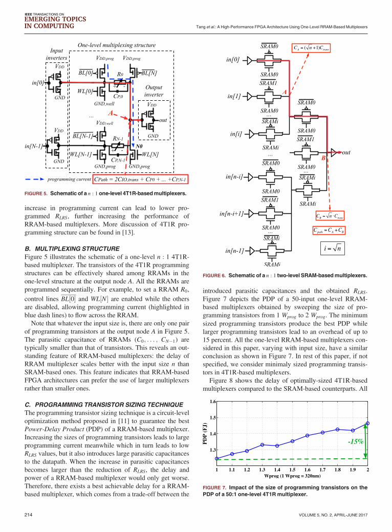
Figure 5 illustrates the schematic of a one-level n : 1 4T1R-based multiplexer. The transistors of the 4T1R programmingstructures can be effectively shared among RRAMs in theone-level structure at the output node A. All the RRAMs areprogrammed sequentially. For example, to set a RRAM R0,
control lines BL½0� and WL½N� are enabled while the othersare disabled, allowing programming current (highlighted inblue dash lines) to flow across the RRAM.Note that whatever the input size is, there are only one pair
of programming transistors at the output node A in Figure 5.The parasitic capacitance of RRAMs (C0; . . . ; CN�1) aretypically smaller than that of transistors. This reveals an out-standing feature of RRAM-based multiplexers: the delay ofRRAM multiplexer scales better with the input size n thanSRAM-based ones. This feature indicates that RRAM-basedFPGA architectures can prefer the use of larger multiplexersrather than smaller ones.
C. PROGRAMMING TRANSISTOR SIZING TECHNIQUE
The programming transistor sizing technique is a circuit-leveloptimization method proposed in [11] to guarantee the bestPower-Delay Product (PDP) of a RRAM-based multiplexer.Increasing the sizes of programming transistors leads to largeprogramming current meanwhile which in turn leads to lowRLRS values, but it also introduces large parasitic capacitancesto the datapath. When the increase in parasitic capacitancesbecomes larger than the reduction of RLRS, the delay andpower of a RRAM-based multiplexer would only get worse.Therefore, there exists a best achievable delay for a RRAM-based multiplexer, which comes from a trade-off between the
introduced parasitic capacitances and the obtained RLRS.Figure 7 depicts the PDP of a 50-input one-level RRAM-based multiplexers obtained by sweeping the size of pro-gramming transistors from 1 Wprog to 2 Wprog. The minimumsized programming transistors produce the best PDP whilelarger programming transistors lead to an overhead of up to15 percent. All the one-level RRAM-based multiplexers con-sidered in this paper, varying with input size, have a similarconclusion as shown in Figure 7. In rest of this paper, if notspecified, we consider minimaly sized programming transis-tors in 4T1R-based multiplexers.Figure 8 shows the delay of optimally-sized 4T1R-based
multiplexers compared to the SRAM-based counterparts. All
FIGURE 6. Schematic of a n : 1 two-level SRAM-basedmultiplexers.
FIGURE 5. Schematic of a n : 1 one-level 4T1R-basedmultiplexers.
FIGURE 7. Impact of the size of programming transistors on the
PDP of a 50:1 one-level 4T1R multiplexer.
214 VOLUME 5, NO. 2, APRIL-JUNE 2017
Tang et al.: A High-Performance FPGA Architecture Using One-Level RRAM-Based Multiplexers
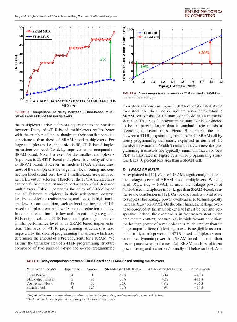
the multiplexers drive a fan-out equivalent to the smallestinverter. Delay of 4T1R-based multiplexers scales betterwith the number of inputs thanks to their smaller parasiticcapacitances than those of SRAM-based multiplexers. Forlarge multiplexers, i.e., input size is 50, 4T1R-based imple-mentations can reach 2� delay improvement as compared toSRAM-based. Note that even for the smallest multiplexers(input size is 2), 4T1R-based multiplexer is as delay efficientas SRAM-based. However, in modern FPGA architectures,most of the multiplexers are large, i.e., local routing and con-nection blocks, and very few 2:1 multiplexers are deployed,i.e., BLE output selector. Therefore, the FPGA architecturescan benefit from the outstanding performance of 4T1R-basedmultiplexers. Table 1 compares the delay of SRAM-basedand 4T1R-based multiplexer in their architectural context,i.e., by considering realistic sizing and loads. In high fan-inand low fan-out condition, such as local routing, the 4T1R-based multiplexer can achieve 48 percent reduction in delay.In contrast, when fan-in is low and fan-out is high, e.g., theBLE output selector, 4T1R-based multiplexer guarantees asimilar performance level as an SRAM-based implementa-tion. The area of 4T1R programming structures is alsoimpacted by the sizes of programming transistors, which alsodetermines the amount of set/reset currents for a RRAM. Weassume the transistor area of a 4T1R programming structurecomposed of two pairs of p-type and n-type programming
transistors as shown in Figure 3 (RRAM is fabricated abovetransistors and does not occupy transistor area) while aSRAM cell consists of a 6-transistor SRAM and a transmis-sion gate. The area of a programming transistor is consideredto be 40 percent larger than a standard logic transistoraccording to layout rules. Figure 9 compares the areabetween a 4T1R programming structure and a SRAM cell bysizing programming transistors, expressed in terms of thenumber of Minimum Width Transistor Area. Since the pro-gramming transistors are typically minimum sized for bestPDP as illustrated in Figure 7, a 4T1R programming struc-ture leads 10 percent less area than a SRAM cell.
D. LEAKAGE ISSUE
As explained in [12], RHRS of RRAMs significantly influencethe leakage power of RRAM-based multiplexers. When asmall RHRS, i.e., ¼ 20MV, is used, the leakage power of4T1R-based multiplexer is 5� larger than SRAM-based, sim-ilar to the conclusion in [12]. On the one hand, a trivial routeto suppress the leakage power overhead is to technologicallyincrease RHRS to 200MV. On the other hand, the leakage over-head observed at the multiplexer level must be put into per-spective. Indeed, the overhead is in fact non-existent in thearchitecture context, because: (a) in high fan-out condition,the leakage power of a multiplexer is much smaller than itslarge output buffers; (b) leakage power is negligible as com-pared to dynamic power and 4T1R-based multiplexers con-sume less dynamic power than SRAM-based thanks to theirlower parasitic capacitances. (c) RRAM enables efficientpower saving and instant-on/normally-off behavior [39]. As a
FIGURE 8. Comparison of delay between SRAM-based multi-
plexers and 4T1R-based multiplexers.
TABLE 1. Delay comparison between SRAM-Based and RRAM-Based routing multiplexers.
Multiplexer Location Input Size fan-out SRAM-based MUX (ps) 4T1R-based MUX (ps) Improvements
Local Routing 80 1 57.7 30.4 �48%BLE output selector 2 70 38.8 42.2 þ11%Connection block 48 60 76.0 48.2 �36%Switch block 4 1241 57.8 49.6 �14%
�Output buffers are considered and sized according to the fan-outs of routing multiplexers in architecture.1The fanout includes the parasitics of long metal wires driven by SBs.
FIGURE 9. Area comparison between a 4T1R cell and a SRAM cell
under differentWprog.
VOLUME 5, NO. 2, APRIL-JUNE 2017 215
Tang et al.: A High-Performance FPGA Architecture Using One-Level RRAM-Based Multiplexers
result, according to [12], although RHRS ¼ 20MV introduces ahigh leakage overhead (5�) to 4T1R-based multiplexers, thetotal power of the resulting RRAM-based FPGA is similar toits SRAM-based counterpart. Therefore, we believe that theconsidered RHRS ¼ 27MV in this paper is large enough to pre-vent any power issues.
V. ARCHITECTURAL OPTIMIZATIONS
As discussed in Section IV, there is a strong need to optimizeFPGA architectures, in order to exploit the high-performanceof 4T1R-based multiplexers. In this section, we propose threearchitectural optimizations: (1) The realization of a UnifiedConnection Block; (2) The increase of Switch Blocks capac-ity; (3) The decrease of the best length of routing wire; Foreach architectural optimization, we study its impact on bothSRAM-based and RRAM-based FPGAs.
A. UNIFIED CONNECTION BLOCK
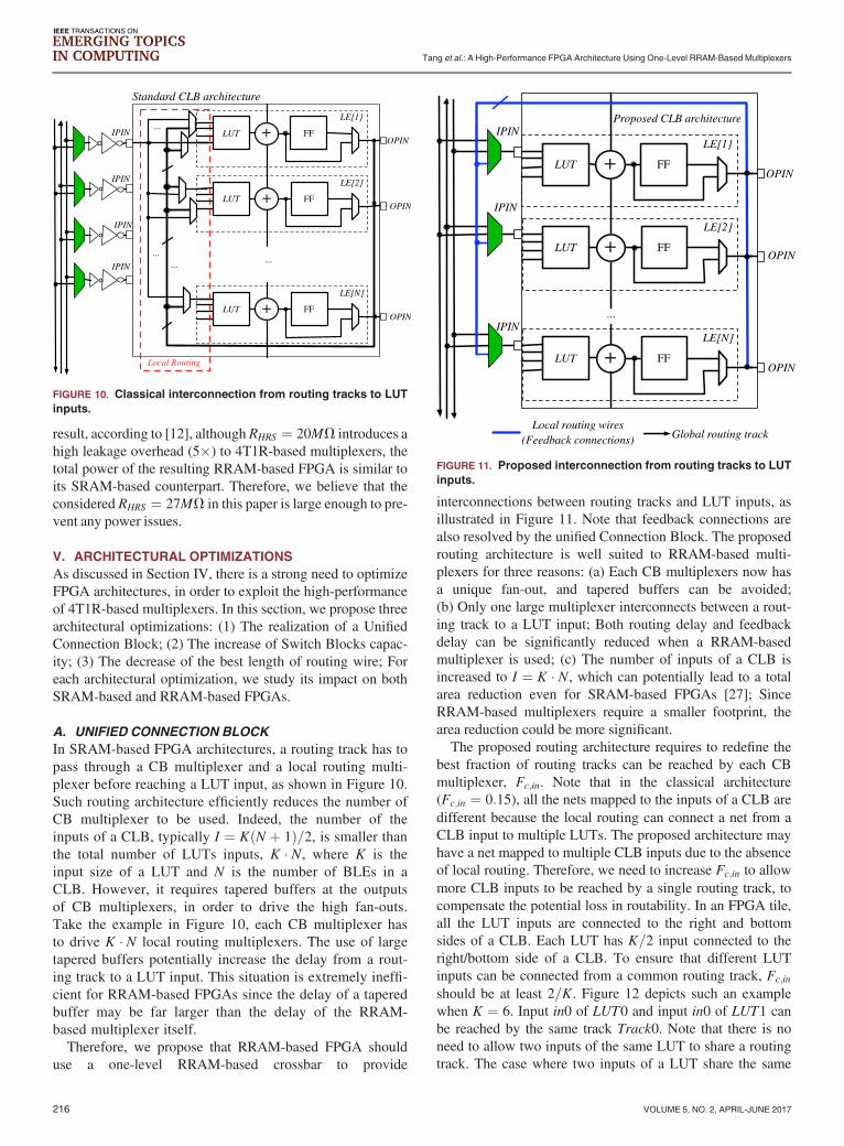
In SRAM-based FPGA architectures, a routing track has topass through a CB multiplexer and a local routing multi-plexer before reaching a LUT input, as shown in Figure 10.Such routing architecture efficiently reduces the number ofCB multiplexer to be used. Indeed, the number of theinputs of a CLB, typically I ¼ KðN þ 1Þ=2, is smaller thanthe total number of LUTs inputs, K � N, where K is theinput size of a LUT and N is the number of BLEs in aCLB. However, it requires tapered buffers at the outputsof CB multiplexers, in order to drive the high fan-outs.Take the example in Figure 10, each CB multiplexer hasto drive K � N local routing multiplexers. The use of largetapered buffers potentially increase the delay from a rout-ing track to a LUT input. This situation is extremely ineffi-cient for RRAM-based FPGAs since the delay of a taperedbuffer may be far larger than the delay of the RRAM-based multiplexer itself.Therefore, we propose that RRAM-based FPGA should
use a one-level RRAM-based crossbar to provide
interconnections between routing tracks and LUT inputs, asillustrated in Figure 11. Note that feedback connections arealso resolved by the unified Connection Block. The proposedrouting architecture is well suited to RRAM-based multi-plexers for three reasons: (a) Each CB multiplexers now hasa unique fan-out, and tapered buffers can be avoided;(b) Only one large multiplexer interconnects between a rout-ing track to a LUT input; Both routing delay and feedbackdelay can be significantly reduced when a RRAM-basedmultiplexer is used; (c) The number of inputs of a CLB isincreased to I ¼ K � N, which can potentially lead to a totalarea reduction even for SRAM-based FPGAs [27]; SinceRRAM-based multiplexers require a smaller footprint, thearea reduction could be more significant.The proposed routing architecture requires to redefine the
best fraction of routing tracks can be reached by each CBmultiplexer, Fc;in. Note that in the classical architecture(Fc;in ¼ 0:15), all the nets mapped to the inputs of a CLB aredifferent because the local routing can connect a net from aCLB input to multiple LUTs. The proposed architecture mayhave a net mapped to multiple CLB inputs due to the absenceof local routing. Therefore, we need to increase Fc;in to allowmore CLB inputs to be reached by a single routing track, tocompensate the potential loss in routability. In an FPGA tile,all the LUT inputs are connected to the right and bottomsides of a CLB. Each LUT has K=2 input connected to theright/bottom side of a CLB. To ensure that different LUTinputs can be connected from a common routing track, Fc;in
should be at least 2=K. Figure 12 depicts such an examplewhen K ¼ 6. Input in0 of LUT0 and input in0 of LUT1 canbe reached by the same track Track0. Note that there is noneed to allow two inputs of the same LUT to share a routingtrack. The case where two inputs of a LUT share the same
FIGURE 10. Classical interconnection from routing tracks to LUT
inputs.
FIGURE 11. Proposed interconnection from routing tracks to LUT
inputs.
216 VOLUME 5, NO. 2, APRIL-JUNE 2017
Tang et al.: A High-Performance FPGA Architecture Using One-Level RRAM-Based Multiplexers

net can never happen because the inputs of a LUT are natu-rally logic equivalent.By considering architecture parameters K ¼ 6, the pro-
posed architecture requires Fc;in to be at least 0.33, in orderto ensure routability. In this part, we sweep Fc;in to examinethe best Fc;in for the proposed architecture.Figures 13(a) and 13(b) show normalized area, delay, power
and channel width of SRAM-based and RRAM-based pro-posed architectures with Fc;in ¼ f0:15; 0:25; 0:33; 0:5g, whencompared to baseline architectures respectively. The SRAM-based proposed architecture with Fc;in ¼ 0:33 produces aslightly better area-delay product (�4 percent) than the classi-cal architecture, but performs worse (+2 percent) in delay. Incontrast, the RRAM-based proposed architecture withFc;in ¼ 0:33 reduces delay by 3 percent and area-delay productby 15 percent, when compared to the classical architecture. Ineither SRAM-based or RRAM-based FPGAs, the proposedarchitecture with Fc;in ¼ 0:33 produces the best area-delayproduct. Note that we see a 5 percent area reduction in bothSRAM-based and RRAM-based proposed architectures whenFc;in ¼ 0:33, which is close to the conclusion of literature [27].The proposed architecture with varying Fc;in reduces power by10-13 percent for SRAM-based and RRAM-based FPGAs. Inthe classical architecture, there are two-stages of multiplexers(local routing and classical connection blocks) that lead to fourlevels of transmission gates between the routing tracks and theLUTs. However, in the proposed unified connection block,there is only one-stage of multiplexers (two-levels of transmis-sion gates) between the routing tracks and the LUTs, contribut-ing to power efficiency. Besides, the unified connection blockseliminates the need for intermediate buffers between the localrouting and the connection block, which further reduce thepower. Channel width overheads are observed in both SRAM-based and RRAM-based proposed architectures, because theirroutability is lower than their baselines due to the absence oflocal routing. However, these overheads can be potentiallyeliminated because the routability can be significantlyimproved when we increase Fs and decrease L. In terms of thebest overall performance, we consider Fc;in ¼ 0:33 for the pro-posed FPGA architectures in the rest of this paper.
Figure 14 compares the tile area of a classical FPGA archi-tecture (I ¼ 40;Fc;in ¼ 0:15) and the proposed RRAMFPGA architecture (I ¼ W � Fc;in;Fc;in ¼ 0:33) for a sweep-ing channel width W from 100 to 350. Note that the inputsize of local routing multiplexers in traditional SRAMFPGAs is fixed for every W , while that of proposed RRAMFPGAs is directly related to W . When a small W , e.g. ¼ 100,is used, the size of the local routing multiplexers in the pro-posed RRAM FPGAs is smaller than for a classical FPGAarchitecture. Therefore, when W < 300, the proposedRRAM FPGA architecture benefits up to 36 percent areareduction as compared to classical FPGA architecture. WhenW > 300, the input size of multiplexers in the proposedRRAM FPGAs becomes larger, leading to a 9 percent areaoverhead when W ¼ 350. The considered W ¼ 320 in thispaper promises that the proposed RRAM FPGAs is as areaefficient as classical SRAM FPGAs.
FIGURE 12. An illustrative example of the proposed routing
architecture (K ¼ 6) with Fc;in ¼ 0:33 and Fs ¼ 6.
FIGURE 13. Normalized average area, delay, power and channel
width of baseline and proposed architecture by sweeping Fc;in:
(a) SRAM-based architectures; (b) RRAM-based architectures.
VOLUME 5, NO. 2, APRIL-JUNE 2017 217
Tang et al.: A High-Performance FPGA Architecture Using One-Level RRAM-Based Multiplexers

B. INCREASE CAPACITY OF SB MUXES
Since RRAM-based multiplexer is more delay-efficient thanSRAM-based multiplexer, the connection flexibility parame-ter of Switch Block Fs can be increased. Classical FPGAarchitectures typically set Fs ¼ 3, where each routing trackon one side of a SB can reach three other routing tracks ondifferent sides of a SB. In SRAM-based FPGAs, Fs ¼ 3promises the best area-delay product [29]. Indeed, a larger Fs
can improve the routability but it may produce area and delayoverhead coming from the larger SB multiplexers to be used.However, considering RRAM-based routing architecture, thedelay overhead is no longer a concern thanks to the advan-tage of RRAM multiplexers. Therefore, a larger Fs, i.e. ¼ 6,can considered, where a routing track can drive six differenttracks, as shown in Figure 12 with Track3. Note that a largeFs significantly improves the routability of the proposed rout-ing architecture. Take the example of Figure 12 where netA isrouted through Track3. If Fs ¼ 3, Track3 can only driveTrack0, Track4 and Track6. If Track0 is not available, theoutput of LUT0 has to seek for another routing track byincreasing the channel width. If Fs ¼ 6, Track3 can reachboth Track0 and Track2. When Track0 is occupied byanother net, Track3 can easily use Track2 to route netA.We sweep Fs to determine its best value for the pro-
posed architecture. Figures 16(a) and 16(b) show normal-ized average area, delay, power and channel width of
SRAM-based and RRAM-based proposed architectureswith Fs ¼ f3; 6; 9g, when compared to the baseline archi-tectures, respectively. The proposed RRAM-based archi-tectures can benefit larger delay reduction (�7 percent)than SRAM-based (�4 percent), because RRAM-basedmultiplexers are more delay efficient for the unified con-nection block. However, Fs > 3 introduces larger SBmultiplexers, which potentially increases the area of bothSRAM-based and RRAM-based proposed architectures.On the other hand, larger SB multiplexers improve theflexibility of the routing architecture and reduce the num-ber of necessary SB multiplexers, as explained inFigure 12. In the end, the proposed architecture can main-tain the same power efficiency as baseline SRAM one.Therefore, Fs ¼ 6 produces the best area-delay-powerproduct for both SRAM-based and RRAM-based proposedarchitectures. Note that, even when Fs ¼ 9, RRAM-basedproposed architecture leads to a 8 percent delay reductionthanks to its RRAM-based multiplexer, while, the SRAM-based proposed architecture has a 5 percent delay over-head. As a large Fs boosts the routability, a 20 percentchannel width reduction is achieved in both SRAM-basedand RRAM-based proposed architectures, as compared tothose with Fs ¼ 3. In terms of the best overall perfor-mance, we consider Fs ¼ 6 for the proposed FPGA archi-tectures in the rest of this paper.
C. SMALLER BEST LENGTHWIRE < 4In FPGA architectures, a length-L wire is a wire that spansacross L CLBs [14]. As illustrated in Figure 15(a), a length-Lwire is driven by an output of CLB½0� and ends atCLB½L� 1�. All the CLBs and SBs along the length-L wirecan be directly routed from the driving output of CLB½0�.When only one type of wires is allowed to be used in anFPGA, the type of length-L wires that produces best area-delay product is called best single wire length. CommercialFPGAs typically provide different types of wires, i.e.,length-1 for short connections and length-8 for long connec-tions. However, best single wire length is useful in decidingwhich type of wires should be predominant within thearchitecture.Length-4 wires are the best choice for classical SRAM-
based FPGA architectures (Fc;in ¼ 0:15;Fs ¼ 3) [14]. Betzet al. show that a length-4 wire is faster than shorter wires interms of delay per logic block (¼ Tdelay;wire=Length). In otherwords, for a routing path spanning X CLBs, length-4 wires
FIGURE 14. Tile area comparison between a traditional FPGA
architecture and the proposed RRAM FPGA architecture for dif-
ferent channel widthW.
FIGURE 15. (a) Driver multiplexer and fan-outs of a Length-L wire; (b) Equivalent RC model of a Length-L wire.
218 VOLUME 5, NO. 2, APRIL-JUNE 2017
Tang et al.: A High-Performance FPGA Architecture Using One-Level RRAM-Based Multiplexers

promise the best average delay. Indeed, when there is a rout-ing path with X < 4, shorter wires such as length-1 orlength-2 will give better delay. However, for a routing pathwith X � 4, multiple cascaded length-4 wires are faster thannot only any length-X (X > 4) wire but also multiple cas-caded length-1 or length-2 wires. Therefore, on average,length-4 wires provide the best trade-off between short andlong connections.In SRAM-based FPGAs, why long length wires, such as
length-4 wires, are preferred is established on the fact thatthe delay of a SB multiplexer is larger than a long metal wireacross a logic block. However, RRAM-based multiplexersare more delay efficient and can be even faster than a longmetal wire. Therefore, as the cost function between a SBmultiplexer and a long metal wire has been twisted, the bestsingle wire length L should be revisited. Figure 15(a) illus-trates the different elements composing a length-L wire,while Figure 15(b) shows the extracted RC model. We use
Elmore delay [31] to estimate the delay per logic block of aLength-L wire
Tdelay;wire=L ¼ 1L
XL�1
i¼0
Ri
XL�1
j¼i
Cj
¼ L � RmCm
2þ 1L� ðTdel þ RoCo � 2RmCSB � 2RmCCBÞ
þ RmðCSB þ CCB � CmÞ þ RoðCm þ CSB þ CCBÞ;(1)
where Rm and Cm are the resistance and capacitance of ametal wire spanning a logic block, respectively, Tdel repre-sents the intrinsic delay of a SB multiplexer, Ro and Co
denote the equivalent resistance and capacitance of thetapered buffer that drives the metal wire, respectively, CSB
and CCB are the equivalent input capacitance of each SB andCB, respectively. According to (1), there exists a Loptimalwhich guarantees the minimum Tdelay;wire=L
Loptimal ¼ ðTdel þ RoCo � 2RmCSB � 2RmCCBÞ2RmCm
: (2)
Note that CSB and CCB are related to Fs and Fc;in respectively
CSB ¼ Fs � Cin
CCB ¼ W � Fc;in � Cin:(3)
In the proposed RRAM-based routing architecture, whereboth Fs and Fc;in increased and Tdel decreased thanks toRRAM-based multiplexer, Loptimal will definitely decrease. Inaddition, the tile area of the proposed architecture may beslightly larger than the classical architecture because of theFs and Fc;in increases, leading to an increased Rm and Cm.This would further decrease the Loptimal. Therefore, the bestsingle wire length of the proposed routing architecture willbe smaller than 4. When a smaller L (< 4) is used, previouswork [14] show that the routability is improved significantly.Therefore, the proposed RRAM-based routing architecturecan achieve routability improvement without delay overhead.We sweep L to determine its best value for the proposed
architecture. Figures 17(a) and 17(b) show normalized aver-age area, delay, power and channel width of SRAM-basedand RRAM-based proposed architectures with L ¼ f1; 2; 4g,when compared to the baseline architectures, respectively. InSRAM-based architectures, whatever Fs is, length-4 wiresachieve the best delays and area-delay-power products. How-ever, the proposed RRAM-based architecture with length-2wires promises the best delay (�11 percent) and also the bestarea-delay-power product (�24 percent), thanks to its betterroutability and lower routing congestion. As L is reducedfrom 4 to 2, we see a 26 percent channel width reductionbecause short wires are more flexible. Conversely, length-1wires have the smallest channel width but more SB multi-plexers have to be used in long routing paths. Therefore, wesee significant area and power overhead. Length-4 wires
FIGURE 16. Normalized average area, delay, power and channel
width of baseline and proposed architectures by sweeping Fs:
(a) SRAM-based architectures; (b) RRAM-based architectures.
VOLUME 5, NO. 2, APRIL-JUNE 2017 219
Tang et al.: A High-Performance FPGA Architecture Using One-Level RRAM-Based Multiplexers
guarantee the best power results since less multiplexers arerequired in a SB compared to the case where length-2 andlength-1 wires are used. In terms of the best overall perfor-mance, L ¼ 2 is the best single wire length for the proposedFPGA architecture.
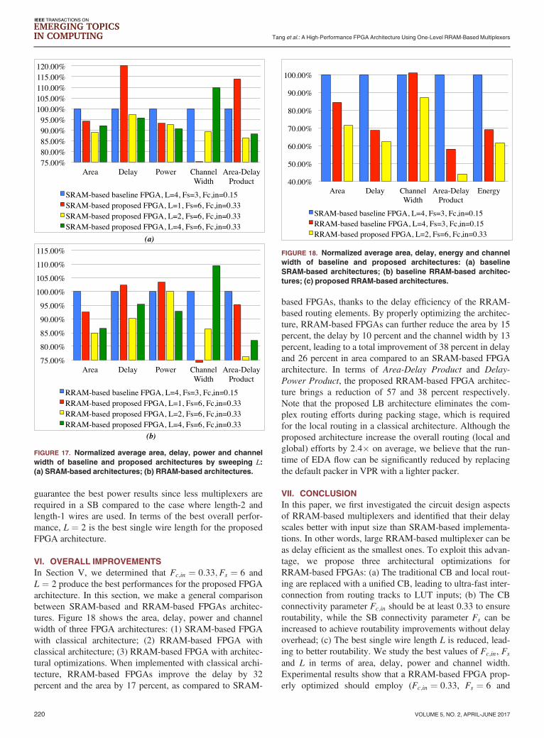
VI. OVERALL IMPROVEMENTS
In Section V, we determined that Fc;in ¼ 0:33;Fs ¼ 6 andL ¼ 2 produce the best performances for the proposed FPGAarchitecture. In this section, we make a general comparisonbetween SRAM-based and RRAM-based FPGAs architec-tures. Figure 18 shows the area, delay, power and channelwidth of three FPGA architectures: (1) SRAM-based FPGAwith classical architecture; (2) RRAM-based FPGA withclassical architecture; (3) RRAM-based FPGA with architec-tural optimizations. When implemented with classical archi-tecture, RRAM-based FPGAs improve the delay by 32percent and the area by 17 percent, as compared to SRAM-
based FPGAs, thanks to the delay efficiency of the RRAM-based routing elements. By properly optimizing the architec-ture, RRAM-based FPGAs can further reduce the area by 15percent, the delay by 10 percent and the channel width by 13percent, leading to a total improvement of 38 percent in delayand 26 percent in area compared to an SRAM-based FPGAarchitecture. In terms of Area-Delay Product and Delay-Power Product, the proposed RRAM-based FPGA architec-ture brings a reduction of 57 and 38 percent respectively.Note that the proposed LB architecture eliminates the com-plex routing efforts during packing stage, which is requiredfor the local routing in a classical architecture. Although theproposed architecture increase the overall routing (local andglobal) efforts by 2:4� on average, we believe that the run-time of EDA flow can be significantly reduced by replacingthe default packer in VPR with a lighter packer.
VII. CONCLUSION
In this paper, we first investigated the circuit design aspectsof RRAM-based multiplexers and identified that their delayscales better with input size than SRAM-based implementa-tions. In other words, large RRAM-based multiplexer can beas delay efficient as the smallest ones. To exploit this advan-tage, we propose three architectural optimizations forRRAM-based FPGAs: (a) The traditional CB and local rout-ing are replaced with a unified CB, leading to ultra-fast inter-connection from routing tracks to LUT inputs; (b) The CBconnectivity parameter Fc;in should be at least 0.33 to ensureroutability, while the SB connectivity parameter Fs can beincreased to achieve routability improvements without delayoverhead; (c) The best single wire length L is reduced, lead-ing to better routability. We study the best values of Fc;in, Fs
and L in terms of area, delay, power and channel width.Experimental results show that a RRAM-based FPGA prop-erly optimized should employ (Fc;in ¼ 0:33, Fs ¼ 6 and
FIGURE 17. Normalized average area, delay, power and channel
width of baseline and proposed architectures by sweeping L:(a) SRAM-based architectures; (b) RRAM-based architectures.
FIGURE 18. Normalized average area, delay, energy and channel
width of baseline and proposed architectures: (a) baseline
SRAM-based architectures; (b) baseline RRAM-based architec-
tures; (c) proposed RRAM-based architectures.
220 VOLUME 5, NO. 2, APRIL-JUNE 2017
Tang et al.: A High-Performance FPGA Architecture Using One-Level RRAM-Based Multiplexers

L ¼ 2) to achieve optimal performances. When considering aclassical architecture for both SRAM-based and RRAM-based FPGAs, an improvement of 32 percent in delay and 17percent in area can be achieved. The proposed architecturaloptimizations can further reduce area by 15 percent, delay by10 percent and channel width by 13 percent, leading to a totalimprovement of Area-Delay Product by 57 percent andDelay-Power Product by 38 percent.
ACKNOWLEDGMENTS
This work was supported by the Swiss National ScienceFoundation under the project number 200021-146600.
REFERENCES
[1] S. S. Sheu, et al., “A 4Mb embedded SLC resistive-RAM macro with7.2ns read-write random-access time and 160ns MLC-access capability,”in Proc. IEEE Int. Solid-State Circuits Conf. Digest Tech. Papers, 2011,pp. 200–202.
[2] A. Kawahara, et al., “An 8Mb multi-layered cross-point ReRAM macrowith 443MB/s write throughput,” in Proc. IEEE Int. Solid-State CircuitsConf. Digest Tech. Papers, 2012, pp. 432–434.
[3] T. Y. Liu, et al., “A 130.7mm2 2-layer 32Gb ReRAM memory device in24nm technology,” in Proc. IEEE Int. Solid-State Circuits Conf. DigestTech. Papers, 2013, pp. 210–211.
[4] R. Fackenthal, et al., “19.7 A 16Gb ReRAM with 200MB/s write and1GB/s read in 27nm technology,” in Proc. IEEE Int. Solid-State CircuitsConf. Digest Tech. Papers, 2014, pp. 338–339.
[5] M. F. Chang, et al., “17.5 A 3T1R nonvolatile TCAM using MLC ReRAMwith sub-1ns search time,” in Proc. IEEE Int. Solid-State Circuits Conf.Digest Tech. Papers, 2015, pp. 1–3.
[6] Y. Liu, et al., “4.7 A 65nm ReRAM-enabled nonvolatile processor with6� reduction in restore time and 4� higher clock frequency using adaptivedata retention and self-write-termination nonvolatile logic,” in Proc. IEEEInt. Solid-State Circuits Conf. Digest Tech. Papers, 2016, pp. 84–86.
[7] S. Tanachutiwat, M. Liu, and W. Wang, “FPGA based on integration ofCMOS and RRAM,” IEEE Trans. Very Large Scale Integr., vol. 19,no. 11, pp. 2023–2032, Nov. 2010.
[8] J. Cong and B. Xiao, “mrFPGA: A novel FPGA architecture with memris-tor-based reconfiguration,” in Proc. IEEE/ACM Int. Symp. NanoscaleArchit., 2011, pp. 1–8.
[9] J. Cong and B. Xiao, “FPGA-RPI: A novel FPGA architecture withRRAM-based programmable interconnects,” IEEE Trans. Very LargeScale Integr. Syst., vol. 22, no. 4, pp. 864–877, Apr. 2014.
[10] P.-E. Gaillardon, D. Sacchetto, S. Bobba, Y. Leblebici, and G. D. Micheli,“GMS: Generic memristive structure for non-volatile FPGAs,” in Proc.IEEE/IFIP 20th Int. Conf. VLSI Syst.-on-Chip, 2012, pp. 94–98.
[11] X. Tang, P.-E. Gaillardon, and G. D. Micheli, “A high-performance low-power near-Vt RRAM-based FPGA,” in Proc. IEEE Int. Conf. Field-Pro-gram. Technol., 2014, pp. 207–215.
[12] X. Tang, P.-E. Gaillardon, and G. D. Micheli, “Accurate power analysisfor near-Vt RRAM-based FPGA,” in Proc. IEEE 25th Int. Conf. Field Pro-gram. Logic Appl., 2015, pp. 174–177.
[13] X. Tang, G. Kim, P.-E. Gaillardon, and G. D. Micheli, “A study on theprogramming structures for RRAM-based FPGA architectures,” IEEETrans. Circuits Syst. I: Reg. Papers, vol. 63, no. 4, pp. 503–516, Apr.2016.
[14] V. Betz, J. Rose, and A. Marquardt, Architecture and CAD for Deep-Sub-micron FPGAs. Berlin, Germany: Springer, 1998.
[15] M. Hutton, et al., “Improving FPGA performance and area using anadaptive logic module,” in Proc. 14th Int. Conf. Field Program. LogicAppl., 2004, pp. 135–144.
[16] Altera Corporation, “Stratix 10 Advance Information Brief,” Jul. 2015,[Online]. Available: https://www.altera.com/en_US/pdfs/literature/hb/stratix-10/S10_TX_FPGA_AIB.pdf
[17] Xilinx Corporation, “Virtex-7 User Guide DS180 (v1.17),” May 2015.[Online]. Available: https://www.xilinx.com/support/documentation/user_guides/ug470_7Series_Config.pdf
[18] H.-S. P. Wong, et al., “Metal-oxide RRAM,” Proc. IEEE, vol. 100, no. 6,pp. 1951–1970, Jun. 2012.
[19] J. Sandrini, et al., “Co-design of ReRAM passive crossbar arrays inte-grated in 180nm CMOS technology,” IEEE J. Emerg. Sel. Topics CircuitsSyst., vol. 6, no. 3, pp. 339–351, Sep. 2016.
[20] Y. Wu, “Resistive switching random access memory (RRAM)—Scaling,materials, and new application,” Ph.D. dissertation, Dept. Elect. Eng.,Stanford Univ., Stanford, CA, USA, 2013.
[21] S. Yu, B. Gao, Z Fang, H. Yu, J. Kang, and H.-S. P.Wong, “A neuromorphicvisual system using RRAMsynaptic devices with sub-pJ energy and toleranceto variability: Experimental characterization and large-scale modeling,” inProc. IEEE Int. ElectronDevices Meeting, 2012, pp. 239–242.
[22] F. M. Puglisi, P. Pavan, L. Larcher, and A. Padovani, “Analysis of RTNand cycling variability in HfO2 RRAM devices in LRS,” in Proc. 44thEur. Solid State Device Res. Conf., 2014, pp. 246–249.
[23] A. Levisse, B. Giraud, J. P. No€el, M. Moreau, and J. M. Portal, “SneakPathcompensation circuit for programming and read operations in RRAM-based CrossPoint architectures,” in Proc. IEEE Non-Volatile MemoryTechnol. Symp., 2015, pp. 1–4.
[24] H. Aziza, M. Bocquet, M. Moreau, and J.-M. Portal, “A built-in self-teststructure (BIST) for resistive RAMs characterization: Application to bipo-lar OxRRAM,” J. Solid-State Electron., vol. 103, pp. 73–78, 2015.
[25] F. M. Puglisi, C. Wenger, and P. Pavan, “A novel program-verify algo-rithm for multi-bit operation in Hf O2 RRAM,” IEEE Electron DeviceLett., vol. 36, no. 10, pp. 1030–1032, Oct. 2015.
[26] E. Lee, G. Lemieux, and S. Mirabbasi, “Interconnect driver design for longwires in field-programmable gate arrays,” J. Signal Process. Syst., vol. 51,no. 1, pp. 57–76, Apr. 2008.
[27] W. Feng and S. Kaptanoglu, “Designing efficient input interconnect blocksfor LUT clusters using counting and entropy,” ACM Trans. ReconfigurableTechnol. Syst., vol. 1, no. 1, Mar. 2008, Art. no. 6.
[28] J. M. Rabaey, A. Chandrakasan, and B. Nikolic, Digital Integrated Cir-cuits, 2nd ed. Englewood Cliffs, NJ, USA: Prentice-Hall, 2002.
[29] G. Lemieux, E. Lee, M. Tom, and A. Yu, “Directional and single-driverwires in FPGA interconnect,” in Proc. IEEE Int. Conf. Field-Program.Technol., 2004, pp. 41–48.
[30] D. Lewis, et al., “Architectural enhancements in Stratix V,” in Proc. ACM/SIGDA Int. Symp. Field Program. Gate Arrays, 2013, pp. 147–156.
[31] W. C. Elmore, “The transient response of damped linear networks withparticular regard to wideband amplifiers,” J. Appl. Phys., vol. 19, no. 1,pp. 55–63, 1948.
[32] C. Chiasson and V. Betz, “Should FPGAs abandon the pass-gate?” inProc. 23rd Int. Conf. Field Program. Logic Appl., 2013, pp. 1–8.
[33] Z. Jiang, S. Yu, Y.Wu, J. H. Engel, X. Guan, and H.-S. P.Wong, “Verilog—A compact model for oxide-based resistive random access memory,” in Proc.IEEE Int. Conf. Simul. Semicond. Processes Devices, 2014, pp. 41–44.
[34] HSPICE User Guide: Simulation and Analysis, Version I-2013.12,Synopsys, Mountain View, CA, USA, Dec. 2013.
[35] Altera Corporation, “Stratix IV device handbook version SIV5V1–1.1,”Jul. 2008. [Online]. Available: http://www.altera.com/literature/hb/stratix-iv/stratix4_handbook.pdf
[36] S. Yang, “Logic synthesis and optimization benchmarks user guide version3.0,”MCNC, Durham, NC, USA, Tech. Rep., Jan. 1991.
[37] J. Rose, et al., “The VTR project: Architecture and CAD for FPGAs fromverilog to routing,” in Proc. ACM/SIGDA Int. Symp. Field Program. GateArrays, 2012, pp. 77–86.
[38] University of California in Berkeley, “ABC: A System for Squential Syn-thesis and Verification,” (2007, Sept.). [Online]. Available: http://www.eecs.berkeley.edu/alanmi/abc/
[39] O. Turkyilmaz, et al., “RRAM-based FPGA for “normally off, instantlyon” applications,” in Proc. IEEE/ACM Int. Symp. Nanoscale Archit.,2012, pp. 101–108.
XIFAN TANG (S’13) received the BSc degree inmicroelectronics from Fudan University, Shanghai,China, in 2011, and theMSc degree in electrical engi-neering from the �Ecole Polytechnique F�ed�erale deLausanne (EPFL), Lausanne, Switzerland, in 2013.He is currently working toward the PhD degree atEPFL. His current research interests include com-puter-aided design for programmable architectureand emerging technologies. He received the 2015Chinese Government Award for Outstanding Self-Financed Students Abroad. He is a student memberof the IEEE.
VOLUME 5, NO. 2, APRIL-JUNE 2017 221
Tang et al.: A High-Performance FPGA Architecture Using One-Level RRAM-Based Multiplexers
GIOVANNI DE MICHELI is a professor anddirector of the Institute of Electrical Engineeringand of the Integrated Systems Centre, EPF Lau-sanne, Switzerland. He is a program leader of theNano-Tera.ch program. Previously, he was a pro-fessor of electrical engineering with Stanford Uni-versity. His research interests include severalaspects of design technologies for integrated cir-cuits and systems, such as synthesis for emergingtechnologies, networks on chips, and 3D integra-tion. He is also interested in heterogeneous plat-
form design including electrical components and biosensors, as well as indata processing of biomedical information. He is author of: Synthesis andOptimization of Digital Circuits, McGraw-Hill, 1994, co-author and/or co-editor of eight other books and of more than 700 technical articles. His cita-tion h-index is 88 according to Google Scholar. He is a member of the Scien-tific Advisory Board of IMEC (Leuven, B), CfAED (Dresden, D), andSTMicroelectronics. He received the 2016 IEEE/CS Harry Goode award forseminal contributions to design and design tools of Networks on Chips, the2016 EDAA Lifetime Achievement Award, the 2012 IEEE/CAS Mac VanValkenburg award for contributions to theory, practice and experimentationin design methods and tools, and the 2003 IEEE Emanuel Piore Award forcontributions to computer-aided synthesis of digital systems. He alsoreceived the Golden Jubilee Medal for outstanding contributions to the IEEECAS Society in 2000, the D. Pederson Award for the best paper on the IEEETransactions on Computer-Aided Design of Integrated Circuits and Systemsin 1987, and several Best Paper Awards, including DAC (1983 and 1993),DATE (2005), and Nanoarch (2010 and 2012). He has been serving IEEE inseveral capacities, namely: Division 1 Director (2008-9), co-founder andpresident elect of the IEEE Council on EDA (2005-7), president of the IEEECAS Society (2003), editor in chief of the IEEE Transactions on Computer-Aided Design of Integrated Circuits and Systems (1997-2001). He has beena chair of several conferences, including Memocode (2014) DATE (2010),pHealth (2006), VLSI SOC (2006), DAC (2000), and ICCD (1989). He is afellow of the ACM and the IEEE and a member of the Academia Europaea.
PIERRE-EMMANUEL GAILLARDON(S’10-M’11) received the electrical engineer degreefrom CPE-Lyon, France, in 2008, the MSc degreein electrical engineering from INSA Lyon, France,in 2008, and the PhD degree in electrical engineer-ing from CEA-LETI, Grenoble, France, and theUniversity of Lyon, France, in 2011. He is an assis-tant professor in the Electrical and Computer Engi-neering (ECE) Department, The University ofUtah, Salt Lake City, Utah, and he leads the Labo-ratory for NanoIntegrated Systems (LNIS). Prior to
joining the University of Utah, he was a research associate with the SwissFederal Institute of Technology (EPFL), Lausanne, Switzerland, within theLaboratory of Integrated Systems (Prof. De Micheli) and a visiting researchassociate with Stanford University, Palo Alto, California. Previously, he wasa research assistant with CEA-LETI, Grenoble, France. He received the C-Innov 2011 best thesis award and the Nanoarch 2012 best paper award. Heis an associate editor of the IEEE Transactions on Nanotechnology. He hasbeen serving as TPC member of many conferences, including DATE’15-16,DAC’16, Nanoarch’12-16, and is reviewer of several journals and fundingagencies. He will serve as Topic co-chair “Emerging Technologies forFuture Memories” for DATE’17. His research activities and interests are cur-rently focused on the development of reconfigurable logic architectures anddigital circuits exploiting emerging device technologies and novel EDA tech-niques. He is a member of the IEEE.
Tang et al.: A High-Performance FPGA Architecture Using One-Level RRAM-Based Multiplexers
222 VOLUME 5, NO. 2, APRIL-JUNE 2017