A High Gain, Low Power, Low Cin/Gain ratio Ultrasonic Receiver using 90 nm Technology
4
I J SR D - I nt e rnat i ona l J o urnal for Scient i fi c R e se a rch & D evelo p m e nt | V o l. 3, I ssue 12, 201 6 | I SSN (online): 232 1-061 3 All rights reserved by www.ijsrd.com 450 A High Gain, Low Power, Low Cin/Gain Ratio Ultrasonic Receiver using 90 nm Technology Virendra Khare 1 Vinod Sonkar 2 Deepak Sharma 3 1 M.Tech. Student 2 Assistant Professor 3 Head of Dept 1,2,3 Department of Electronics & Communication Engineering 1,2,3 SDBCT, Indore Abstract — Ultrasonic receiver have been best option for many application like biomedical wearable device, indoor location sensing, tracking etc. The design of analog front end design for wearable application is important for the performance of system. In this paper, receiver is shown designed on 90 nm technology . Results simulated on tanner tool shows 45.32 dB at bandwidth of 48.33 kHz. Cin/Gain parameter is calculated which is 27.1. All the r esults shows that it would be a good design for biomedical application. K ey wo r ds: Ultrasonic Receiver, Ultrasonic Receiver Circuit I. I NTRODUCTION Ultrasonic transducers are traditionally used in Wireless Sensor Systems (WSN) for biomedical and also industrial applications with regard to remote powering and also perform wireless transmission to implanted receptors, range finding and also object detection and also tracking etc. Fig. 1 illustrates a normal compliance zone as well as the sensor systems stationed to enforce compliance. Fig. 1: Zonal compliance system A person or object entering the zone needs to be equipped with a new wearable device to get the information transmitted from your zonal transmitters or from your interactive stations including washers (as found in Fig. 1) furnished with transmitters. Fundamental blocks of such the zonal compliance system is composed of an ultrasonic transducer primarily based zonal transmitter and also an ultrasonic transducer primarily based wearable device and also their associated digital and analog software circuits as found in Fig. 1. Schematic diagram of the Ultrasonic telemetry technique is shown with Fig. 2. At the actual receiver the transducer turns the sound force variations into comparative electrical signal. The lowest noise front stop amplifier and subsequent gain stages together boosts the weak signal acquired because of the transducer. A limit detection circuit then the gain stages helps you to recover a clean signal through the noisy received indication. Fig. 2: Block diagram of an ultrasonic telemetry system II. LITERATURE SURVEY Woradorn Wattanapanitch et al. (2007) designed a low noise amplifier by designing bandpass filter followed by gain stage. Low noise is obtained because of low noise OTA design to obtain gain of 40dB and OTA is designed using low supply current. Zhang Xu et al. (2010) shown amplifier with 20 dB gain and DC gain of 0 dB by c apacitive coupled and capacitive feedback topology with bandwidth of 6.7 kHz in a 0.35 m process and because of this, it was possible to integrated preamplifier on same die. The bandwidth of amplifier can be tuned by pseudo-resistor for low field potential (Vikram Chaturvedi et al.(2011)). By adopting this method, they achieve mid band gain of 37 dB and minimise the attenuation of signal from neuron to the gate of input transistor. They have also used fully differential configuration to reject noise and to achieve high PSRR. Fan Zhang et al.(2012) compare three bio potential amplifier. Out of those, bio potential amplifer 3 was choosen to be the best because of low input noise referred and adoptable power consumption and for this reasons, this amplifier used f or low powe r wireless system that has been deployed in many experiments. Kian Ann Ng et al.(2013) choose telescopic cascade OTA architecture and with that, he obtain low input noise referred with output swing of 40 mV for a 500mV neural signal. Noushin Ghaderi et al. (2014) design the bulk- driven amplifier that improves output swing significantly with less power consumption and noise factor. He designed on 180nm CMOS technology. He increased output swing by reducing the voltage drop on the amplifier load and for that, he designed bulk-driven cascade current mirror as a load. Kian Ann Ng et al.(2013) presented another paper which increase the mid band gain by finding the ratio between input capacitance and gain and by replacing feedback capacitor with T-capacitor network. It tells about the area require by amplifier as well as about the gain. He obtains the gain of 38.7 dB with ratio of 20. He proposed that the smaller the ratio, better will be the value of gain as well as smaller area.
-
Upload
international-journal-for-scientific-research-and-development-ijsrd -
Category
Documents
-
view
216 -
download
0
Transcript of A High Gain, Low Power, Low Cin/Gain ratio Ultrasonic Receiver using 90 nm Technology

7/26/2019 A High Gain, Low Power, Low Cin/Gain ratio Ultrasonic Receiver using 90 nm Technology
http://slidepdf.com/reader/full/a-high-gain-low-power-low-cingain-ratio-ultrasonic-receiver-using-90-nm 1/3
I JSRD - I nternational Journal for Scientifi c Research & Development| Vol. 3, I ssue 12, 2016 | ISSN (onli ne): 2321-0613
All rights reserved by www.ijsrd.com 450
A High Gain, Low Power, Low Cin/Gain Ratio Ultrasonic Receiver using
90 nm TechnologyVirendra Khare1 Vinod Sonkar2 Deepak Sharma3 1M.Tech. Student 2Assistant Professor 3Head of Dept
1,2,3Department of Electronics & Communication Engineering1,2,3
SDBCT, Indore Abstract — Ultrasonic receiver have been best option for
many application like biomedical wearable device, indoor
location sensing, tracking etc. The design of analog front
end design for wearable application is important for the
performance of system. In this paper, receiver is shown
designed on 90 nm technology. Results simulated on tanner
tool shows 45.32 dB at bandwidth of 48.33 kHz. Cin/Gain
parameter is calculated which is 27.1. All the results shows
that it would be a good design for biomedical application.
Key words: Ultrasonic Receiver, Ultrasonic Receiver Circuit
I. I NTRODUCTION
Ultrasonic transducers are traditionally used in WirelessSensor Systems (WSN) for biomedical and also industrial
applications with regard to remote powering and also
perform wireless transmission to implanted receptors, range
finding and also object detection and also tracking etc. Fig.
1 illustrates a normal compliance zone as well as the sensorsystems stationed to enforce compliance.
Fig. 1: Zonal compliance system
A person or object entering the zone needs to be
equipped with a new wearable device to get the information
transmitted from your zonal transmitters or from your
interactive stations including washers (as found in Fig. 1)furnished with transmitters. Fundamental blocks of such the
zonal compliance system is composed of an ultrasonic
transducer primarily based zonal transmitter and also an
ultrasonic transducer primarily based wearable device and
also their associated digital and analog software circuits as
found in Fig. 1. Schematic diagram of the Ultrasonic
telemetry technique is shown with Fig. 2.
At the actual receiver the transducer turns the
sound force variations into comparative electrical signal.The lowest noise front stop amplifier and subsequent gain
stages together boosts the weak signal acquired because of
the transducer. A limit detection circuit then the gain stages
helps you to recover a clean signal through the noisy
received indication.
Fig. 2: Block diagram of an ultrasonic telemetry system
II. LITERATURE SURVEY
Woradorn Wattanapanitch et al. (2007) designed a low noiseamplifier by designing bandpass filter followed by gain
stage. Low noise is obtained because of low noise OTA
design to obtain gain of 40dB and OTA is designed using
low supply current. Zhang Xu et al. (2010) shown amplifier
with 20 dB gain and DC gain of 0 dB by capacitive coupled
and capacitive feedback topology with bandwidth of 6.7
kHz in a 0.35 m process and because of this, it was possible to integrated preamplifier on same die.
The bandwidth of amplifier can be tuned by
pseudo-resistor for low field potential (Vikram Chaturvedi
et al.(2011)). By adopting this method, they achieve mid
band gain of 37 dB and minimise the attenuation of signalfrom neuron to the gate of input transistor. They have also
used fully differential configuration to reject noise and to
achieve high PSRR.
Fan Zhang et al.(2012) compare three bio potential
amplifier. Out of those, bio potential amplifer 3 was choosen
to be the best because of low input noise referred and
adoptable power consumption and for this reasons, this
amplifier used for low power wireless system that has been
deployed in many experiments.
Kian Ann Ng et al.(2013) choose telescopic
cascade OTA architecture and with that, he obtain low input
noise referred with output swing of 40 mV for a 500mV
neural signal. Noushin Ghaderi et al. (2014) design the bulk-
driven amplifier that improves output swing significantly
with less power consumption and noise factor. He designed
on 180nm CMOS technology. He increased output swing by
reducing the voltage drop on the amplifier load and for that,
he designed bulk-driven cascade current mirror as a load.
Kian Ann Ng et al.(2013) presented another paper
which increase the mid band gain by finding the ratio
between input capacitance and gain and by replacing
feedback capacitor with T-capacitor network.
It tells about the area require by amplifier as well
as about the gain. He obtains the gain of 38.7 dB with ratio
of 20. He proposed that the smaller the ratio, better will bethe value of gain as well as smaller area.
7/26/2019 A High Gain, Low Power, Low Cin/Gain ratio Ultrasonic Receiver using 90 nm Technology
http://slidepdf.com/reader/full/a-high-gain-low-power-low-cingain-ratio-ultrasonic-receiver-using-90-nm 2/3
A High Gain, Low Power, Low Cin/Gain Ratio Ultrasonic Receiver using 90 nm Technology
(IJSRD/Vol. 3/Issue 12/2016/117)
All rights reserved by www.ijsrd.com 451
Haridas Kuruveettil et al. (2013 ) designed the
ultrasonic transducer for biomedical application ,indoor
location sensing, tracking and other compliance purpose at180 nm with 3 V supply. Operational amplifier and OTA is
designed with bias current of 2 A with receiver output of0V-3V square wave. He’s transducer consume less power
as compared to discrete component based receiver.
III.
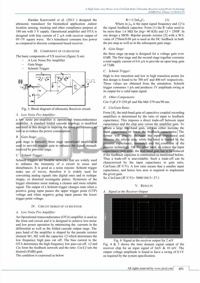
COMPONENT OF US RECEIVER
The basic components of US receiver (figure 3) are:
A Low Noise Pre Amplifier
Gain Stage
Schmitt Trigger
Fig. 3: Block diagram of ultrasonic Receiver circuit.
A. Low Noise Pre-Amplifier:
a low noise pre-amplifier is operational transconductanceamplifier. A standard folded cascode topology is modified
and used in this design to improve the noise performance as
well as to reduce the power consumption.
B. Gain Stage:
gain stage is basically three stage operational amplifier is
used to provide require gain to enhance the signal strength
received by previous stage.
C. Schmitt Trigger:
Schmitt triggers are bistable networks that are widely used
to enhance the immunity of a circuit to noise and
disturbances. It is good as a noise rejecter. Schmitt trigger
make use of waves, therefore it is widely used for
converting analog signals into digital ones and to reshape
sloppy, or distorted rectangular pulses. Hysteresis of the
trigger eliminates noise making a cleaner and more reliable
signal. The output of a Schmitt trigger changes state when a
positive going input passes the upper trigger point (UTP)voltage and when negative going input passes the lower
trigger point voltage.
IV. CIRCUIT DESIGN OF US RECEIVER
A. Low Noise Pre-Amplifier:
An Operational transconductance (OTA) amplifier is used as
the front end circuit and it is designed to achieve low-noiseand low power operation by minimizing the currents in the
differential as well as the folded cascade output stage .The
pass band of the amplifier is shaped by the pseudo resistor
element M1, M2 with the capacitor Cf which determines the
low frequency high pass cut off. The bias current to the
OTA determines the high frequency low pass cut off. Cf and
Cin form the feedback network and the ratio Cin/Cf sets thedesired (45dB) gain.
The condition is expressed as below
R>>1/2πf sigCf (1)
Where in f sig is the input signal frequency and Cf is
the signal feedback capacitor. From (1) the R value need to be more than 1.6 MΩ for f sig= 40 KHz and Cf = 250fF. In
our design a MOS- Bipolar pseudo resistor [5] with a W/L
value of 270nm/0.09 μm is used as the DC feedback in both
the pre amp as well as in the subsequent gain stage.
B.
Gain Stage:the three stage op-amp is designed for a voltage gain over63dB. The first stage and the second stage together consume
a total supply current of 6.6 μA to provide an open loop gain
of 73dB.
C. Schmitt Trigger:
High to low transition and low to high transition points for
this design is found to be 700 mV and 400 mV respectively.These values are obtained from the simulation. Schmitt
trigger consumes 1 pA and produces 1V amplitude swing at
its output for a valid input signal.
D. Other Components:
Cin=5 pF,Cf=250 pF and Ma-Md=270 nm/90 nm.
E. Cin/Gain Ratio:
From [4], the mid-band gain of capacitive coupled recording
amplifiers is determined by the ratio of input to feedback
capacitance. This imposes a direct trade-off between input
capacitance and the chip area versus the amplifier gain. To
obtain a large mid-band gain, we can either increase theinput capacitance or lower the feedback capacitance. The
former will directly decrease the input impedance and
increase the silicon area, while the latter is limited by the
parasitic capacitance, mismatch and the constraint of the
process technology. On the other hand, to reduce the inputcapacitance (and area), the mid-band gain has to be reduced
if the feedback capacitor is constrained as mentioned before.
Thus a trade-off is unavoidable. Such a trade-off can be
characterized by the input capacitance to gain ratio,
Cin/Gain (fF.V/V). A low ratio means that a smaller input
capacitance, and hence less area is required to implement
the given gain. So, Cin/Gain (fF.V/V)= 5000/184.5= 27.1
V. R ESULTS
A. Signal at the Receiver Output
Fig. 4: Signal at the receiver output for 2 mV
Fig. 4 & 5 shows the time domain signal output of the
receiver chip for an input signal of 2mV & 10 mV. Theoutput voltage amplitude is found to have a swing of 0-1V
as required by the system specification.
7/26/2019 A High Gain, Low Power, Low Cin/Gain ratio Ultrasonic Receiver using 90 nm Technology
http://slidepdf.com/reader/full/a-high-gain-low-power-low-cingain-ratio-ultrasonic-receiver-using-90-nm 3/3
A High Gain, Low Power, Low Cin/Gain Ratio Ultrasonic Receiver using 90 nm Technology
(IJSRD/Vol. 3/Issue 12/2016/117)
All rights reserved by www.ijsrd.com 452
Fig. 5: signal at the receiver output for 10 mV
B. Frequency Response of Receiver
Fig. 6: Frequency response of receiver
Fig.6 showing dc gain of 45.32dB with f L=25.82KHz &
f H=74.37 KHz and BW=48.33 KHz at Cin=5.0pF,
Cfb=250fF. So the Cin/Gain (fF.V/V) = 5000/184.5=27.1
C. Noise Response of Receiver
Fig. 7: Total noise referred of US receiver
Fig.7 indicating total noise inferred by receiver is 525
aV/Hz at 24.82 KHz-74.37KHz which is very less ascompared by any other receiver.
Fig. 8: output referred noise of US receiver
Fig.8 indicating output noise inferred by receiver is32 nV/Hz at 24.82KHz-74.37KHz
VI. CONCLUSION
In this paper, the design methodology and measurement
result of an analog front end circuit for an ultrasonic
receiver is presented which used in a battery powered
wearable device of a zonal compliance sensor system.Measured results shows that the power consumption is very
less and reduces the number of components used and
thereby the size of the wearable device at very low outputand total noise referred.
ACKNOWLEDGMENT
It is my privilege to acknowledge those who helped and
guided me throughout my journey of this research. I am
thankful to Mr. Vinod Sonkar, Dept. of Electronics andCommunication, SDBCT, Indore without their guidance and
generous support this work wouldn’t have been possible. I
am also thankful to Mr. Deepak Sharma, HOD, Dept. Of
Electronics and Communication, SDBCT, Indore for their
able supervision.
R EFERENCES
[1] Woradorn Wattanapanitch, Michale Fee, Rahul
Sarpeshkar, “An Energy-Efficient Micropower Neural
Recording Amplifier,” IEEE transactions on
Biomedical Circuits and Systems, Vol. 1, no. 2, June
2007.
[2] Noushin Ghaderi, Sayed-Mahdi Kazemi-Ghahfarokhi,
“A Low Power, Low Noise Neural Amplifier, UsingBulk-driven Cascode Current Mirror Load,”
[3] Fan Zhang, Jeremy Holleman, Brian P. Otis, “Design of
Ultra-Low Power Biopotential Amplifiers for Biosignal
Acquisition Applications,” IEEE transactions on
Biomedical Circuits and Systems, Vol. 6, no. 4, August2012.
[4] K ian Ann Ng, Yong Ping Xu, “A Compact, Low Input
Capacitance Neural Recording Amplifier with Cin/Gain
of 20fF.V/V,”
[5] K. A. Ng, Yong Ping Xu, “A Compact, Low Input
Capacitance Neural Recording Amplifier,” IEEE
transactions on Biomedical Circuits and Systems, Vol.
7, no. 5, October 2013.
[6] Zhang Xu, Pei Weihua, Huang Beiju, Chen Hongda,
“Low power CMOS preamplifier for neural recording
applications,” Journal of Semiconductors, Vol. 31, No.
4 , April 2010.
[7]
Vikram Chaturvedi, Bharadwaj Amrutur, “A Low- Noise Low-Power Noise-Adaptive Neural Amplifier in
0.13um CMOS technology,” 24th Annual Conference
on VLSI Design, IEEE Computer Society, 2011.