A High Efficiency and High Voltage Gain DC-DC Converter...
12
A High Efficiency and High Voltage Gain DC-DC Converter for Renewable Energy Connected to Induction Motor M. Suresh * and Y.P. Obulesu ** Abstract: In recent days, the renewable resources like Solar and fuel cell stacks are mostly considered for operating at low voltages. Thus, grid coupled systems uses these resources with voltage boosting resulting in performance reduction. In order to solve this issue this paper proposes a concept of coupled inductor based DC-DC converter which has high efficiency. This converter consists of passive clamped network and it has the capability to increase the voltage gain as well as efficiency of the system. The voltage stress on the switch is reduced by the presence of a passive clamp network. The output of the proposed dc-dc converter is converted to three phase voltage which is suitable for grid interconnection via SVPWM based VSC converter and it is operated to load of three phase induction motor. The proposed work has been implemented using MATLAB/Simulink Software. To valid the proposed scheme simulation results are presented. Keywords: Coupled Inductor based Clamping Circuit, High Voltage Gain and Solar Photovoltaics. INTRODUCTION 1. In the present scenario, power quality and power supply are the main problems in power system. So that, the DG systems has got lot of importance because of the limitation of conventional power generation. The main advantage of DG system, it is more productive, high quality, and provide power to loads to maintain continuous administration. Therefore, the PV system is considered as an infinite, uncontaminated alternative resource. In PV systems, there is a possibility to convert direct sun energy to electrical energy without any interruptions. The efficiency of the solar system can be improved by using general MPPTs. The frequently used MPP techniques are given below: 1. P&O Technique. 2. INC Technique. 3. Fuzzy based MPPT Technique. The maximum utilization of power electronic systems can produce nonlinearity in network, and its effects on overall system performance. To mitigate problems caused by harmonics, some filter components are used inside the system. In this paper Figure 1 shows a photovoltaic system that is a combination of solar array, a high step-up converter, a charge-discharge controller and an inverter. Basically, the previous conventional step-up converters, such as the boost converter and fly-back converter, cannot achieve a high step-up conversion of energy at cost of high efficiency due to the elements used in the converter configuration. And also maximum power point tracking (MPPT) techniques are used for improving the performance of PV systems, a high efficiency power converter which is designed to extract maximum power from a PV panel is usually considered. This paper presents an efficient MPPT * P.G Student, K.L. University, Vaddeswaram, Guntur, India. Email: [email protected] ** Professor, K.L. University, Vaddeswaram, Guntur, India. Email: [email protected] I J C T A, 10(5) 2017, pp. 947-957 © International Science Press
Transcript of A High Efficiency and High Voltage Gain DC-DC Converter...

A High Efficiency and High Voltage Gain DC-DC Converter for Renewable Energy Connected to Induction MotorM. Suresh* and Y.P. Obulesu**
Abstract: In recent days, the renewable resources like Solar and fuel cell stacks are mostly considered for operating at low voltages. Thus, grid coupled systems uses these resources with voltage boosting resulting in performance reduction. In order to solve this issue this paper proposes a concept of coupled inductor based DC-DC converter which has high efficiency. This converter consists of passive clamped network and it has the capability to increase the voltage gain as well as efficiency of the system. The voltage stress on the switch is reduced by the presence of a passive clamp network. The output of the proposed dc-dc converter is converted to three phase voltage which is suitable for grid interconnection via SVPWM based VSC converter and it is operated to load of three phase induction motor. The proposed work has been implemented using MATLAB/Simulink Software. To valid the proposed scheme simulation results are presented.
Keywords: Coupled Inductor based Clamping Circuit, High Voltage Gain and Solar Photovoltaics.
INTRODUCTION1. In the present scenario, power quality and power supply are the main problems in power system. So that, the DG systems has got lot of importance because of the limitation of conventional power generation. The main advantage of DG system, it is more productive, high quality, and provide power to loads to maintain continuous administration. Therefore, the PV system is considered as an infi nite, uncontaminated alternative resource. In PV systems, there is a possibility to convert direct sun energy to electrical energy without any interruptions. The efficiency of the solar system can be improved by using general MPPTs. The frequently used MPP techniques are given below:
1. P&O Technique.
2. INC Technique.
3. Fuzzy based MPPT Technique.
The maximum utilization of power electronic systems can produce nonlinearity in network, and its effects on overall system performance. To mitigate problems caused by harmonics, some fil ter components are used inside the system.
In this paper Figure 1 shows a photovoltaic system that is a combination of solar array, a high step-up converter, a charge-discharge controller and an inverter.
Basically, the previous conventional step-up converters, such as the boost converter and fly-back converter, cannot achieve a high step-up conversion of energy at cost of high efficiency due to the elements used in the converter configuration. And also maximum power point tracking (MPPT) techniques are used for improving the performance of PV systems, a high efficiency power converter which is designed to extract maximum power from a PV panel is usually considered. This paper presents an efficient MPPT * P.G Student, K.L. University, Vaddeswaram, Guntur, India. Email: [email protected]** Professor, K.L. University, Vaddeswaram, Guntur, India. Email: [email protected]
I J C T A, 10(5) 2017, pp. 947-957© International Science Press

948 M. Suresh and Y.P. Obulesu
controller for PV systems by incorporating a new design of high step-up boost converter controlled by a different MPPT methods such as fuzzy and Incremental Conductance algorithm. The high step-up boost converter is useful for use in a transformer less three phase PV inverter which needs 700-900 V DC supply input to give 415 AC output.
Figure 1: High step-up converter.
GRID-INTERFACED SYSTEM OR LOAD2. In this paper a PV based hybrid system with various controllers is considered, sustaining power to a load and the network as appeared in Figure 2 where CDC is the dc link capacitor.
From the above discussions we can conclude that the high efficiency boost converter is very essential which must be kept at the front end and connected right across the PV panel as shown in Figure 2 below.
Figure 2: Block diagram of a PV power conversion system
In the present scenario, due to increasing of energy demands and higher reliability of requirements are move to concentrate on the utilization of DG systems as an alternate solution. In rural areas the most useful DG sources as PV, Wind and Fuel Cell generation systems. Nowadays, the PV power systems is the feasible solution to the clean bulk power to grids out of all renewable systems because of the following advantages. The PV generation supports not only being clean and renewable but also it have low running and maintain cost. Figure 2 shows the grid connected hybrid system.
Photovoltaic Array ModelingIn the PV network of electrical phenomenon, cell is the necessary part. For the raise in appropriate current, high power and potential difference, the sunlight dependent cells and their region unit joined in non-current or parallel fashion called as PV exhibit are used. In practical applications, each and every cell is similar to diode with the intersection designed by the semiconductor material. When the light weight is absorbed by the electrical marvel sway at the point of intersection, it gives the streams at once. The (current-voltage) and (Power-Voltage) attributes at absolutely unpredictable star intensities of the PV exhibit are represented in Figure 3, whereas the often seen existence of most electrical outlet on each yield is shown in power diagram 2.
I = Iph - ID - Ish (1)
I = Iph - I0[exp(q ¥ VD/nKT)] - (VD/Rs) (2)

949A High Efficiency and High Voltage Gain DC-DC Converter for Renewable Energy Connected to Induction Motor
Figure 3: PV Electrical Equivalent circuit
Solar cell output power is given as the product of V and I
(a) (b)
Figure 4: (a) and (b) output characteristics of PV Array
CONVERTER TOPOLOGIES OF HIGH VOLAGE GAIN DC-DC CONVERTERS3. The converters shown in Figure 1 depict some of the high voltage gain topologies that are representative of the existing configurations. Direct voltage step up using high frequency transformer renders a simple and easily controllable converter providing high gain. Isolated current-fed dc-dc converters are example of this category. However these topologies result in high voltage spikes across the switch (due to leakage inductance) and large ripple in primary side transformer current as the turns ratio in the high frequency transformer increases. The isolated systems are relatively costly, bulky and generally less efficient even though they offer more safety, eliminate issues such as ground leakage current and can provide multiple outputs among other advantages. Most of the non-isolated high voltage gain dc-dc power converters employ coupled inductor (to achieve higher voltage gain) in contrast to a high frequency transformer used by the isolated versions [Figure 1]. The coupled inductor based dc-dc converter has advantages over isolated transformer based dc-dc converter in minimizing current stress, using lower rating components and simple winding structure. Modeling procedure of the coupled inductor is described. The energy recovered from the leakage inductance can be calculated from the following equation:[3]
12
L IL2
lk (3)
Where Llk is leakage inductance is IL is the inductor current and Lm is the magnetizing inductance given by:
Llk = (1 - k)L; Lm = kL (4)
K is the coupling coefficient and L is the inductance.
Voltage across clamp capacitor, C, can be calculated from (3):
12
L IL2
lk = 12
CVC2 (5)

950 M. Suresh and Y.P. Obulesu
Where, C and VC are the clamping capacitance and clamp voltage, respectively.
The conventional DC-DC converter have following disadvantages:
1. It produces large peak current to flow on the input side, which adversely affects the magnetic components and results in high losses.
2. It causes large voltage to appear across the switch. As the on state resistance of a switch depends on its voltage rating [RDSon µ V2
DS], the conduction losses increase. Due to large duty cycle, the losses in parasitic resistances of inductance and capacitance also increase.
3. Diode reverse recovery becomes a major concern. In view of the above, there is clearly a need to develop and use special high gain, high efficiency dc-dc converters to implement MPPT and to step up voltage level. Several circuit topologies have been proposed for this application. They follow one or more of the following philosophies to achieve high voltage at the converter output.
(a) Direct voltage step-up using high frequency transformer.
(b) Use of coupled inductor to utilize the energy storage capability of the magnetizing inductance of the core to increase the voltage level using turns ratio of the coupled inductor.
(c) Use of interleaved coupled inductor that facilitates use of smaller inductors, division of current and higher effective inductance for higher power applications.
(d) Active and passive clamp circuits to recover leakage energy in the coupled inductor based high gain converters to reduce losses in leakage inductance.
(e) Use of intermediate energy storage capacitors as additional buffers to increase the voltage gain without increasing duty cycle to high value. A brief overview of the high voltage gain topologies reported in the literature is presented in the next section.
DESCRIPTION OF PROPOSED CONVERTER4. Energy conversion efficiency of solar PV is quite low (about 12–25%) [2]. Therefore, it is essential to use a highly efficient power conversion system to utilize the PV generated power to the maximum. The proposed high gain dc-dc converter configuration is shown in Figure 5. It consists of one passive clamp network, a coupled inductor (L1, L2) and an intermediate capacitor apart from other components.
Figure 5: Circuit diagram of proposed DC-DC Converter
The symbol VPV represents the PV voltage applied to the circuit. S is the main switch of the proposed converter. The coupled inductor’s primary and secondary inductors are denoted by L1 and L2. C1 and D1 represent the passive clamp network across L1. The capacitor CO is the output capacitor while D3 is the output diode. The voltage V0 is the average (dc) output across the load. The intermediate energy storage capacitor, C2 and the feedback diode D2 are connected on the secondary side.

951A High Efficiency and High Voltage Gain DC-DC Converter for Renewable Energy Connected to Induction Motor
The gain ratio, n is given by:
n = VV
L2
L1 (6)
Where, VL1 and VL2 represent the voltages across inductors L1 and L2. The operating modes for continuous conduction mode (CCM) are shown in Figure 4. Various operating modes are described below:
Mode 1 & 2[t0 – t1]: The switch (S) is turned on at the start of the converter operation[2]. The current flows through the switch and the primary side of the coupled inductor (L1), energizing the magnetizing inductance (Lm) of the coupled inductor. The current path is as shown in Figure 6 (I). The two diodes, D1 and D3 are reverse biased, while D2 is forward biased during this mode. The intermediate capacitor, C2 is charged through D2 by L2 and capacitor, C1. If voltage across intermediate capacitor (C2) becomes equal to the summation of voltages across L2 and C1, diode D2 turns off. The current flowing through Lm (iLm) in this mode may be obtained by using the following relation:
iLm(t) = V
L L Li
m kmt t i t
+- +( ) ( )0 0 (7)
Figure 6: Equivalent Circuit Configuration for mode (i) & (ii)
The parasitic capacitance of the switch S is charged by the magnetizing current flowing through the inductor L1. The diode D2 remains forward biased and current continues to flow through this. Current path in this mode is shown in Figure 6(ii).The magnetizing inductance current for this mode is given by the following equation:
iLm(t) = V
L L Li
m kmt t i t
+- +( ) ( )1 1 (8)
Mode 3 [t2 – t3]: In this mode, diodes D1 and D3 become forward biased. D2 is reverse biased and its current becomes zero in this mode. The leakage energy stored in the primary side of the coupled inductor (L1) is recovered and stored in the clamp capacitor (C1) through D1. Also, the energy is transferred from the input side to the output side through diode D3 as shown in Figure 7 (III). The recovered leakage inductance current (iLk) is given by:
iLk(t) = V
L LC
L1
2 2m k
mt t i t+
- +( ) ( ) (9)

952 M. Suresh and Y.P. Obulesu
Figure 7: Equivalent Circuit Configuration for mode (iii)
Mode 4 [t3 – t4]: This mode begins after the completion of recovery of the leakage energy from inductor L1. The diode D1 now becomes reverse biased while diode D3 remains forward biased in this mode. The current flows from the input side to the output side to supply the load as shown in Figure 8 (IV). The current iLm flowing through secondary inductor (L2) is given by the following equation:
iLm(t) = V V
LVC
L0 2
3 3- -
- +i
mmn
t t i t( ) ( ) (10)
Figure 8: Equivalent Circuit Configuration for mode (iv)
Mode 5 [t4 – t0]: This mode begins by turning on switch S. The leakage inductor energizes quickly using the full magnetizing current while the parasitic capacitance across the switch discharges in this mode. The two diodes D1 and D2 are in reverse biased condition. The current flow path in this mode is shown in Figure 9 (V). This mode ends when diode D3 becomes reverse biased and current flow through inductor, L2 changes direction. The secondary inductor current (iLm) continues to flow in this mode and current is given by:
iLm(t) = V V
LVC
L0 2
4 4- -
- +i
mmn
t t i t( ) ( ) (11)
Since the current through an inductor iLk = VL L
i
m k
t t( )-+
4 cannot change instantaneously, current rises
slowly. The voltage (VDS) across the switch ‘S’ cannot change instantaneously and decreases slowly.
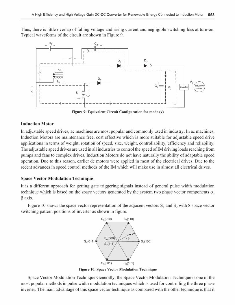
953A High Efficiency and High Voltage Gain DC-DC Converter for Renewable Energy Connected to Induction Motor
Thus, there is little overlap of falling voltage and rising current and negligible switching loss at turn-on. Typical waveforms of the circuit are shown in Figure 9.
Figure 9: Equivalent Circuit Configuration for mode (v)
Induction MotorIn adjustable speed drives, ac machines are most popular and commonly used in industry. In ac machines, Induction Motors are maintenance free, cost effective which is more suitable for adjustable speed drive applications in terms of weight, rotation of speed, size, weight, controllability, efficiency and reliability. The adjustable speed drives are used in all industries to control the speed of IM driving loads reaching from pumps and fans to complex drives. Induction Motors do not have naturally the ability of adaptable speed operation. Due to this reason, earlier dc motors were applied in most of the electrical drives. Due to the recent advances in speed control methods of the IM which will make use in almost all electrical drives.
Space Vector Modulation TechniqueIt is a different approach for getting gate triggering signals instead of general pulse width modulation technique which is based on the space vectors generated by the system two phase vector components a, b axis.
Figure 10 shows the space vector representation of the adjacent vectors S1 and S2 with 8 space vector switching pattern positions of inverter as shown in figure.
Figure 10: Space Vector Modulation Technique
Space Vector Modulation Technique Generally, the Space Vector Modulation Technique is one of the most popular methods in pulse width modulation techniques which is used for controlling the three phase inverter. The main advantage of this space vector technique as compared with the other technique is that it

954 M. Suresh and Y.P. Obulesu
has less harmonic content in both output voltage and current. First the signals from the three phase system is transformed to two phase quantities and then these signals are applied for generating gate pulses for the three phase inverter using space vector modulation technique. Space vector PWM can be implemented by the following steps:
1. Transform 3-phase to 2-phase quantity and determine Vs and angle.
2. Determine time duration T1, T2 and T0.
The reference space vector V* is given by Equation where T1, T2 are the intervals of application of vector S1 and S2 respectively, and zero vectors S0 and S7 are selected for T0.
V* Tz = S1 ¥ T1 + S2 ¥ T2 + S0 ¥ (T0/2) + S7 ¥ (T0/2) (12)
SIMULATION RESULTS AND DISCUSSION5. In above Simulink model the PV array in solar panel is having irradiation and ambient temperature set at 1000 W/m2 and 25°C. The maximum voltage is drawn from PV module by using MPPT is 40V. Normally when the basic boost converter is connected to output of the PV panel it raises approximately to 160V. For proposed boost converter is connected to output of the PV panel it raises to 400V. It means that the proposed converter gain voltage is 10. Whereas the basic boost converter efficiency is 85%, And overall efficiency of the proposed converter is around 95%, It is improved by 10% it means we can save the input energy by 10% finally the better way is to improve the efficiency rather than increase in input energy.
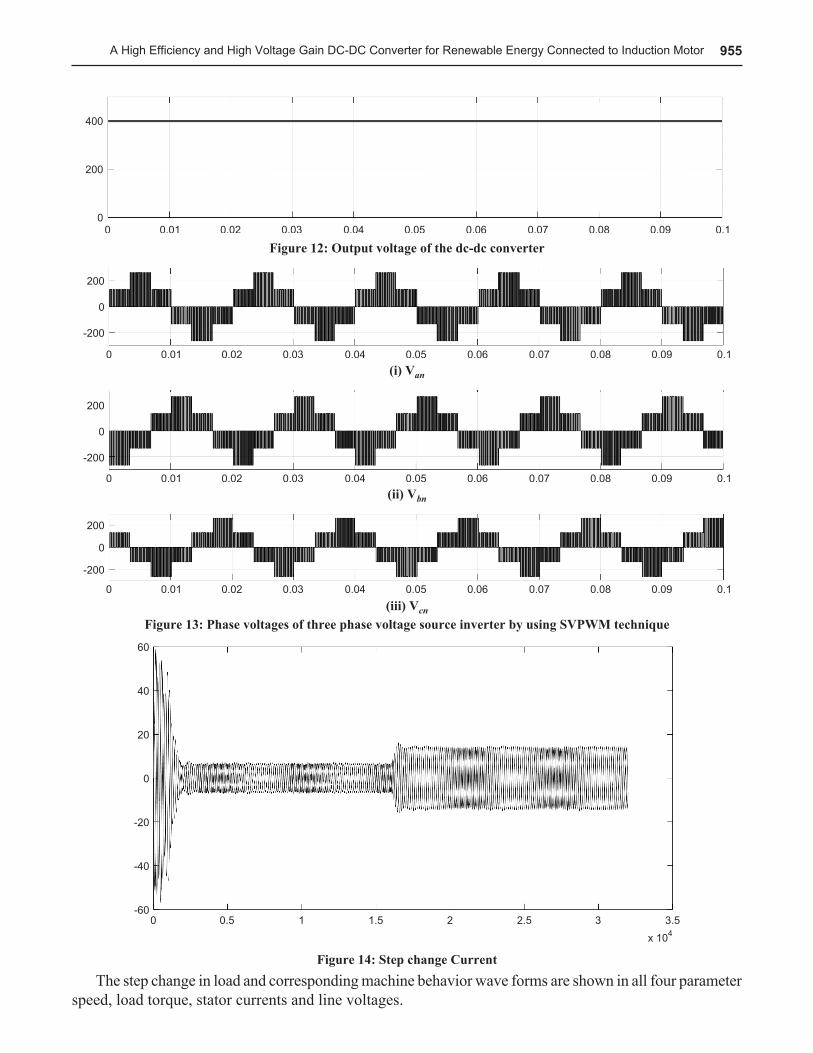
Here the output of dc-dc converter is 400v and this dc voltage is inverted to ac voltage by means of inverter. The function of inverter to convert input dc to output ac voltage. The advantage of inverter is it provides reactive power and even it provides variable voltage and variable frequency. This variable voltage and variable frequency obtained by means of PWM method. The advantage of PWM method to shift the lower order harmonic to high order harmonics and the high order harmonics eliminated by means of filter and finally it is connected to Grid or standalone loads like induction motor. In the Figure 14 speed curve of induction motor shown below. Here the speed curve increasing linearly and maintained constant.
Figure 11: Output voltage of the solar PV system
955A High Efficiency and High Voltage Gain DC-DC Converter for Renewable Energy Connected to Induction Motor
Figure 12: Output voltage of the dc-dc converter
(i) Van
(ii) Vbn
(iii) VcnFigure 13: Phase voltages of three phase voltage source inverter by using SVPWM technique
Figure 14: Step change CurrentThe step change in load and corresponding machine behavior wave forms are shown in all four parameter
speed, load torque, stator currents and line voltages.

956 M. Suresh and Y.P. Obulesu
Figure 15: Line voltage
Figure 16: Step change in Load Torque
Figure 17: Induction Motor Rotor Speed

957A High Efficiency and High Voltage Gain DC-DC Converter for Renewable Energy Connected to Induction Motor
CONCLUSION6. A high efficiency high gain boost converter can be used for DC Grids as well as AC Grids by using inverter. In DC-DC converter, a high voltage gain and high efficiency obtained by coupled inductor, intermediate capacitor and leakage energy recovery. To obtain high voltage gain, there is no necessity to vary excessive duty cycle so that we can reduces the on-state drops across the switch (MOSFET). Using the passive clamp network reduces the voltage stress on the switch. This advantage helps us to use less rating of the switch and reduce the cost of the switch, finally it improves the overall efficiency of the DC-DC converter. The proposed scheme is three phase voltage source inverter helps us to get required voltage and frequency to Grids and stand-alone loads (i.e. Induction Motor). In the proposed technique, a SVPWM based inverter is used which it improves the voltage and frequency profiles at output. The SVPWM based inverter helps to shift lower order harmonics to higher order and thus higher order eliminated by filters. An induction motor subjected to a step change in load, No-Load and Rated Load and their corresponding wave forms along with line voltage and stator currents are also shown. The applied load change in a step at 0.8sec and we can observe the change in behavior of the machine speed, torque and currents.
ReferencesB. Brooks and C. Whitaker, 1. Guideline for the Use of the Performance Test Protocol for Evaluating Inverters Used in Grid-Connected Photovoltaic Systems, Tech. Rep., KEMA-X energy and BEW Engineering, Feb. 25, 2005.Moumita Das2. ; Vivek Agarwal, “Design and Analysis of a High-Efficiency DC– DC Converter with Soft-Switching Capability for Renewable Energy Applications Requiring High Voltage Gain”, “IEEE Transactions on Industrial Electronics”, November 22, 2015. W. Li, and X. He, “Review of Non-isolated High-Step-Up DC/DC Converters in Photovoltaic Grid connected Applications,” 3. IEEE Trans. Ind. Electron., Vol. 58, No. 4, pp. 1239-1250, April 2011.Q. Zhao and F.C. Lee, “High-efficiency, high step-up dc-dc converters,” 4. IEEE Trans. Power Electron., Vol. 18, No. 1, pp. 65-73, Jan. 2003.J.H. Lee, T.J. Liang and J.F. Chen, “Isolated Coupled-Inductor- Integrated DC–DC Converter With Non dissipative Snubber 5. for Solar Energy Applications,” IEEE Trans. Ind. Electron., Vol. 61, No. 7, pp. 3337-3348, July 2014.M. Prudente, L.L. Pfitscher, G. Emmendoerfer, E. F. Romaneli and R. Gules, “Voltage Multiplier Cells Applied to Non-6. Isolated DC–DC Converters,” IEEE Trans. Power Electron., Vol. 23, No. 2, pp. 871-887, Mar. 2008.P.W. Lee, Y.S. Lee, D.K.W. Cheng, and X.C. Liu, “Steady-state analysis of an interleaved boost converter with coupled 7. inductors,” IEEE Trans. Ind. Electron., Vol. 47, pp. 787-795, Aug. 2000.S. Lee, P. Kim and S. Choi, “High step-up soft-switched converters using voltage multiplier cells,” 8. IEEE Trans. Power Electron., Vol. 28, No. 7, pp. 3379-3387, Jul. 2013.C.M. Young, M.H. Chen, T.A. Chang, C.C. Ko and K.K. Jen, “Cascade Cockcroft–Walton Voltage Multiplier Applied 9. to Transformer less High Step-Up DC–DC Converter,” IEEE Trans. Ind. Electron., Vol. 60, No. 2, pp. 523-537, Feb. 2013.M. Das and V. Agarwal, “A novel, high efficiency, high gain, front end DC-DC converter for low input voltage solar 10. photovoltaic applications,” in Proc. IEEE IECON, pp.5744-5749, 25th-28th Oct. 2012.C.T. Pan, C.F. Chuang and C.C. Chu “A Novel Transformer-less Adaptable Voltage Quadruple DC Converter with Low 11. Switch Voltage Stress”, IEEE Trans. Power Electron., Vol. 29, No. 9, pp. 4787-4796, Sept. 2014.K.W. Ma and Y.S. Lee, “An integrated fly-back converter for dc uninterruptible power supply,” 12. IEEE Trans. Power Electron., Vol. 11, pp. 318-327, March 1996.