a high accuracy high throughput jitter test solution - McGill University
10
Paper 12.2 INTERNATIONAL TEST CONFERENCE 1-4244-1128-9/07/$25.00 ©2007 IEEE 1 A HIGH ACCURACY HIGH THROUGHPUT JITTER TEST SOLUTION ON ATE FOR 3GBPS AND 6GBPS SERIAL-ATA Yongquan Fan 1 , Yi Cai 1 and Zeljko Zilic 2 1 LSI Corporation 1110 American Parkway NE, Allentown, Pennsylvania 18109 Email: [email protected] 2 Department of ECE, McGill University ABSTRACT Jitter test in production is notorious for its long test time and the challenge of accuracy verification. Among various types of jitter, Random Jitter (RJ) is most challenging to test on Automatic Test Equipment (ATE) because of its randomness. To be considered as a favorable jitter test in production for multi-gigabit devices, the RJ needs to be measured with sub-picosecond accuracy and the whole test time is expected to be in a few tens of milliseconds. However, no known solutions meet these criteria to our best knowledge. In this paper, we present a systematic solution for multiple Giga-bit-per-second (Gbps) Transmitter (TX) jitter testing on ATE. Our undersampling-based solution extracts jitter either from edge histograms in time domain or from the jitter spectrum in frequency domain. Both approaches provide a RJ precision better than ±0.5ps and are capable of finishing the whole TX test within 100ms. We have verified the solution with data rates up to 6Gbps and applied it in mass production. 1. INTRODUCTION Jitter is the deviation of a signal from its ideal timing. It is composed of both deterministic and random contents. Random Jitter (RJ) is caused by random events and is usually characterized statistically. Deterministic Jitter (DJ) is caused by deterministic events. Major DJ sources include Periodic Jitter (PJ), Duty Cycle Distortion (DCD) and Inter- Symbol Interference (ISI). PJ is caused by repetitive noise sources, such as clock signals and oscillators. DCD is caused by an imbalance in the drive circuit. ISI is caused by frequency related losses in the signal path, such as those caused by the bandwidth limitation. Most communication standards, such as Serial ATA (SATA), Fiber Channel and XAUI, specify jitter in terms of DJ and TJ as separate specifications. TJ is the total jitter, which is associated with a certain Bit Error Rate (BER) level. Table 1 summarizes the TX jitter specifications for the SATA II [1], which directly determine the jitter test limits we should set. The TJ of the SATA TX should not exceed 0.3UI at 10 -12 BER level and DJ should not exceed 0.17UI. Though the SATA specification does not specify the RJ limit, we can get the limit by assuming all TJ is contributed by RJ. The RJ with 0.3UI peak-to-peak value at 10 -12 BER level translates into a RJ root-mean-square (RMS) value of 0.021UI, or 7.0ps at 3Gbps data rate and 3.5ps at 6Gbps data rate. The RJ RMS value is usually used to estimate TJ at 10 -12 BER level, as it is impossible to directly measure TJ at this BER level in volume production due to long test time – it takes a few tens of minutes even for 6Gbps data rate. Table 1. TX Jitter specifications in SATA II TJ DJ RJ (RMS)* 0.3UI 0.17UI 0.021UI or 7.0ps@3G *Deduced from TJ specification To economically apply these test limits in production, we need the jitter test to have the following capabilities: o Separating jitter components o Achieving accuracy in sub-picoseconds o Having the test done in milliseconds Unfortunately, there is currently no solution on ATE that meets there criteria to our best knowledge, even though the jitter measurement and decomposition have been investigated for years [10], [12]. Popular jitter testing solutions include Bit Error Rate Testers (BERT), histogram-based Oscilloscopes, and Time Interval Analyzers (TIA) [2]. These solutions are commonly used for design validation and characterization on bench. However, we can not directly apply them for at-speed testing in production because of the low throughput. For multi-gigabit Serializer/Deserializer (SerDes) testing in production, the most common practice is to loop the output of the transmitter to the input of the receiver either internal to the device or through the loadboard [3], [4]. Its function is checked by comparing the output of the receiver to the expected result. This loopback test can cover the major functionality of SerDes devices. Because of its simplicity and high throughput, the loopback test is very popular and in
Transcript of a high accuracy high throughput jitter test solution - McGill University

Paper 12.2 INTERNATIONAL TEST CONFERENCE 1-4244-1128-9/07/$25.00 ©2007 IEEE
1
A HIGH ACCURACY HIGH THROUGHPUT JITTER TEST SOLUTION
ON ATE FOR 3GBPS AND 6GBPS SERIAL-ATA
Yongquan Fan1, Yi Cai1 and Zeljko Zilic2
1 LSI Corporation 1110 American Parkway NE,
Allentown, Pennsylvania 18109 Email: [email protected]
2 Department of ECE, McGill University
ABSTRACT
Jitter test in production is notorious for its long test time and the challenge of accuracy verification. Among various types of jitter, Random Jitter (RJ) is most challenging to test on Automatic Test Equipment (ATE) because of its randomness. To be considered as a favorable jitter test in production for multi-gigabit devices, the RJ needs to be measured with sub-picosecond accuracy and the whole test time is expected to be in a few tens of milliseconds. However, no known solutions meet these criteria to our best knowledge. In this paper, we present a systematic solution for multiple Giga-bit-per-second (Gbps) Transmitter (TX) jitter testing on ATE. Our undersampling-based solution extracts jitter either from edge histograms in time domain or from the jitter spectrum in frequency domain. Both approaches provide a RJ precision better than ±0.5ps and are capable of finishing the whole TX test within 100ms. We have verified the solution with data rates up to 6Gbps and applied it in mass production. 1. INTRODUCTION Jitter is the deviation of a signal from its ideal timing. It is composed of both deterministic and random contents. Random Jitter (RJ) is caused by random events and is usually characterized statistically. Deterministic Jitter (DJ) is caused by deterministic events. Major DJ sources include Periodic Jitter (PJ), Duty Cycle Distortion (DCD) and Inter-Symbol Interference (ISI). PJ is caused by repetitive noise sources, such as clock signals and oscillators. DCD is caused by an imbalance in the drive circuit. ISI is caused by frequency related losses in the signal path, such as those caused by the bandwidth limitation. Most communication standards, such as Serial ATA (SATA), Fiber Channel and XAUI, specify jitter in terms of DJ and TJ as separate specifications. TJ is the total jitter, which is associated with a certain Bit Error Rate (BER) level. Table 1 summarizes the TX jitter specifications for the SATA II [1], which directly determine the jitter test
limits we should set. The TJ of the SATA TX should not exceed 0.3UI at 10-12 BER level and DJ should not exceed 0.17UI. Though the SATA specification does not specify the RJ limit, we can get the limit by assuming all TJ is contributed by RJ. The RJ with 0.3UI peak-to-peak value at 10-12 BER level translates into a RJ root-mean-square (RMS) value of 0.021UI, or 7.0ps at 3Gbps data rate and 3.5ps at 6Gbps data rate. The RJ RMS value is usually used to estimate TJ at 10-12 BER level, as it is impossible to directly measure TJ at this BER level in volume production due to long test time – it takes a few tens of minutes even for 6Gbps data rate. Table 1. TX Jitter specifications in SATA II
TJ DJ RJ (RMS)*
0.3UI 0.17UI 0.021UI or 7.0ps@3G
*Deduced from TJ specification To economically apply these test limits in production, we need the jitter test to have the following capabilities:
o Separating jitter components o Achieving accuracy in sub-picoseconds o Having the test done in milliseconds
Unfortunately, there is currently no solution on ATE that meets there criteria to our best knowledge, even though the jitter measurement and decomposition have been investigated for years [10], [12]. Popular jitter testing solutions include Bit Error Rate Testers (BERT), histogram-based Oscilloscopes, and Time Interval Analyzers (TIA) [2]. These solutions are commonly used for design validation and characterization on bench. However, we can not directly apply them for at-speed testing in production because of the low throughput. For multi-gigabit Serializer/Deserializer (SerDes) testing in production, the most common practice is to loop the output of the transmitter to the input of the receiver either internal to the device or through the loadboard [3], [4]. Its function is checked by comparing the output of the receiver to the expected result. This loopback test can cover the major functionality of SerDes devices. Because of its simplicity and high throughput, the loopback test is very popular and in

Paper 12.2 INTERNATIONAL TEST CONFERENCE 2
many cases it is also the only widely used test to cover a SerDes device/block. However, the loopback test can not provide any knowledge of parametrical characteristics, including jitter performance. We can only assume that these specifications are “guaranteed by design”. Unfortunately, this assumption is no longer valid while we keep advancing the semiconductor technology and increasing the data rate, which results in tightening the jitter budget. The devices can increasingly fail just because they do not comply with the jitter specifications. It is hence becoming imperative to include jitter test in production in order to distinguish bad devices from good ones. This is the only way to ensure the device quality and to eliminate or reduce customer returns. There are no many choices right now that can do multi-gigabit devices jitter compliance testing in production. Most jitter test solutions are based on lab instruments, extra on-chip circuitry, or DUT board add-on modules [13-16]. These solutions are limited either by its low throughput, low accuracy and repeatability, or by the high design complexity of the device or the loadboard. Because of these limitations, pure ATE-based solutions are preferred in production because of their high portability and high throughput. In recent years, multi-gigabit signal generators and digitizers/samplers are becoming available as fully-integrated ATE instruments. One example is the GigaDig on Catalyst/Tiger ATE from Teradyne [9]. The GigaDig is a digitizer, capable of capturing analog signals with a time resolution better than 1ps. With this kind of instruments, it has become feasible to perform multi-gigabit devices jitter test on ATE [6-8], even though systematic jitter extraction algorithms on ATE have not matured. The jitter performance of a SerDes device can be characterized by the jitter in the output of the transmitter and the jitter tolerance of the receiver. In [6], a TX jitter test solution is proposed based on the high-speed digital pins of the Agilent’s 93000 ATE. By shifting the compare strobes in the timing axis, this approach first builds a bathtub curve, and then applies the jitter separation algorithm. However, the test economy of this solution needs to be improved: it takes near 1 second even with 2ps resolution. As jitter is just one of hundreds parameters to be tested on an average device, one second spent for one test is still too long on the ATE environment. In addition, the accuracy also needs to be improved: RJ is near 1ps higher than the bench result. In [7], an SATA test solution on ATE is presented, which includes TX jitter testing. However, the TX jitter testing scheme in [7] is not very accurate; it reports higher RJ (1~2 ps) and higher TJ (20ps) than the bench equipment does. In addition, the test parameters in this solution can still be further optimized to achieve better test economy.
In [8], we presented a receiver jitter tolerance test solution on ATE, which is capable of accelerating jitter tolerance test by 1000 times. In this paper, we present a new TX jitter testing solution on ATE. With the current ATE instruments, we achieve sub-picosecond accuracy and reduce test time to 0.1s in 3G and 6G applications, which no one else has ever achieved in an ATE environment to our best knowledge. Better performance and higher speed applications are attainable using our solution with the advances in the ATE instruments in the future – they are only limited by the bandwidth and timing resolution of the digitizer. The accuracy of the solution is verified by both bench equipment and ATE itself, and the test has already been applied in volume production. The remainder of the paper presents the details of our TX jitter test solution. In Section 2, we describe the principles of setting test parameters for data acquisition. Section 3 details the data processing – how jitter is separated and decomposed in both the time domain and the frequency domain. We present the experimental results and limitations in Section 4. Section 5 draws conclusions.
2. TEST SETUP FOR DATA ACQUISITION
Our jitter test solution utilizes the GigaDig that is available on Teradyne ATE [9]. Similar instruments are also available from other ATE vendors. The GigaDig is a fully integrated ATE digitizing instrument with a typical undersampling bandwidth over 9 GHz. Its input voltage range is 64mv to 1.024v (the SATA TX output range is 400mv to 700mv). With a 1 Mega sample memory and 12-bit digitizing resolution, the GigaDig is capable of testing the TX jitter for all SATA applications: 1.5Gbps, 3Gbps and 6Gbps. Using the GigaDig, we can perform all TX function and parameter tests with a single capture of the TX output.
Figure 1. Test setup for data acquisition
The test setup is shown in Figure 1. The ATE provides a reference clock signal tx_ref_clk to the transmitter; a PLL in the TX then locks the TX output rate to the reference clock. In our applications, the ideal tx_ref_clk is 30MHz and the TX output data rate FDATA can be 1.5G, 3G or 6G. The GigaDig

Paper 12.2 INTERNATIONAL TEST CONFERENCE 3
captures the TX output with an undersampling rate Fs
between 5 Mega Samples per second (MS/s) to 10 MS/s. DJ, RJ and TJ can be extracted from captured samples. The undersampling technique has been used in high-speed testing for years [10]. This technique first captures the output signal of the DUT at a sampling rate Fs that is lower than the output data rate FDATA, and then shuffles the captured samples in a predetermined manner. The shuffled output is a sequence of samples that would have resulted from sampling at a much higher frequency - effective sampling rate Feff. Although the undersampling principle is simple, the challenges are how to properly set test parameters for data acquisition and how to extract jitter information from captured samples. To capture within reasonable test time the TX output waveform of an adequate resolution for jitter decomposition, we need to properly set these parameters:
o Test pattern length N o Effective sampling rate Feff o Number of samples o Undersampling rate Fs
To provide adequate test coverage, the test pattern length N should be at least 20 bits because the width of the parallel data to the TX input is 20. On the other hand, the length should be as short as possible in order to save test time and also simplify the data processing. For these reasons, we choose a 20-bit test pattern 000001111101010011. This pattern includes both high density and low density transitions, with a total of eight edges. When the 20-bit test pattern is used at a data rate of FDATA=3GHz, the TX output (GigaDig input) fundamental frequency FDUT is
MHzN
FF DATA
DUT 150== (1)
The required effective sampling rate Feff is determined by our target test accuracy. To achieve a jitter measurement resolution better than 1ps, we need to have the effective sampling resolution better than 1ps, which corresponds to an effective sampling rate Feff higher than 1000GHz. For 3GHz data signals, this translates into capturing at least 333 samples per data bit. To leave some margin and also keep test time short, we choose to capture 400 samples per bit, which results in
GHzFF DATAeff 1200*400 == (2)
The required minimum number of samples can be calculated based on the pattern length and the effective sampling rate. To build its edge transition histograms and acquire their statistical properties with a reasonable confidence level, we need to capture at least 20 cycles of the test pattern. Twenty cycles of the 20-bit pattern with 400 samples per bit translate into 160k samples in total. Another factor that we need to consider when determining the total
number of sample is the Fast Fourier Transformation (FFT) requirement. We need FFT later for jitter decomposition in frequency domain. The above derived number of samples satisfies this requirement. The undersampling rate Fs needs to be calculated based on the GigaDig input fundamental frequency FDUT and the effective sampling rate Feff. In order to capture samples coherent with the input signal, we need to satisfy the equation
effDUTs FFK
F
111+= (3)
where K is the number of cycles of FDUT slipped to the next sample. As shown in Figure 1, the ATE sources the reference clock tx_ref_clk to the TX. Ideally, the clock should be 30MHz and the TX output rate would be exactly 3GHz. However, the ATE can not source a clock signal exactly at 30MHz as this clock is derived from the Optical Reference Clock (ORC) divided by t0_clk_div, where ORC=50,000THz and t0_clk_div can only be an integer. For this reason, we need to keep the ratio of FDUT and Feff instead of taking the ideal frequencies when applying Equations (1) and (2) to Equation (3). The ATE clock dividers in Figure 1 are programmed according Equation (3) and other ATE requirements. Table 2 lists the test parameters derived.
Table 2. Testing parameters for 3Gbps signals TX Ref.
Clock (MHz) Undersampling
clock (MHz) Test
pattern Samples per bit
Total samples
30.010564 7.502594038 20bits 400 160k
3. JITTER EXTRACTION In this section, we describe how the jitter is extracted based on the acquired TX waveform with the test setup and the parameters discussed in Section 2. Figure 2 is an example of the captured waveform of a 3G signal. The waveform consists of 20 cycles of the 20-bit test pattern, with 400 samples in each data bit and 160,000 samples in total. This capture is used to perform all TX function and parameter tests. In this paper, we only address jitter testing. Other measurements, such as function, rise/fall time and pre-emphasis, are fast and straightforward once we capture the TX output waveform.
Figure 2. Captured TX signal (unit: mV)
Paper 12.2 INTERNATIONAL TEST CONFERENCE 4
3.1 Generating Edge Displacement
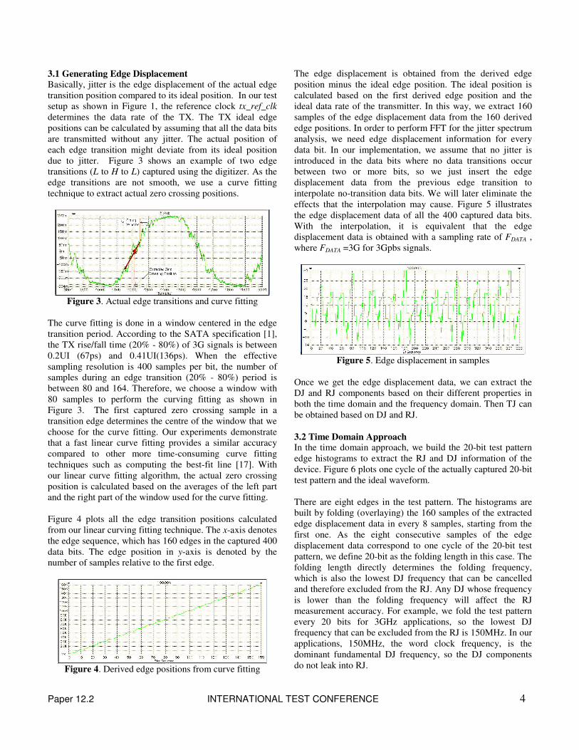
Basically, jitter is the edge displacement of the actual edge transition position compared to its ideal position. In our test setup as shown in Figure 1, the reference clock tx_ref_clk determines the data rate of the TX. The TX ideal edge positions can be calculated by assuming that all the data bits are transmitted without any jitter. The actual position of each edge transition might deviate from its ideal position due to jitter. Figure 3 shows an example of two edge transitions (L to H to L) captured using the digitizer. As the edge transitions are not smooth, we use a curve fitting technique to extract actual zero crossing positions.
Figure 3. Actual edge transitions and curve fitting
The curve fitting is done in a window centered in the edge transition period. According to the SATA specification [1], the TX rise/fall time (20% - 80%) of 3G signals is between 0.2UI (67ps) and 0.41UI(136ps). When the effective sampling resolution is 400 samples per bit, the number of samples during an edge transition (20% - 80%) period is between 80 and 164. Therefore, we choose a window with 80 samples to perform the curving fitting as shown in Figure 3. The first captured zero crossing sample in a transition edge determines the centre of the window that we choose for the curve fitting. Our experiments demonstrate that a fast linear curve fitting provides a similar accuracy compared to other more time-consuming curve fitting techniques such as computing the best-fit line [17]. With our linear curve fitting algorithm, the actual zero crossing position is calculated based on the averages of the left part and the right part of the window used for the curve fitting. Figure 4 plots all the edge transition positions calculated from our linear curving fitting technique. The x-axis denotes the edge sequence, which has 160 edges in the captured 400 data bits. The edge position in y-axis is denoted by the number of samples relative to the first edge.
Figure 4. Derived edge positions from curve fitting
The edge displacement is obtained from the derived edge position minus the ideal edge position. The ideal position is calculated based on the first derived edge position and the ideal data rate of the transmitter. In this way, we extract 160 samples of the edge displacement data from the 160 derived edge positions. In order to perform FFT for the jitter spectrum analysis, we need edge displacement information for every data bit. In our implementation, we assume that no jitter is introduced in the data bits where no data transitions occur between two or more bits, so we just insert the edge displacement data from the previous edge transition to interpolate no-transition data bits. We will later eliminate the effects that the interpolation may cause. Figure 5 illustrates the edge displacement data of all the 400 captured data bits. With the interpolation, it is equivalent that the edge displacement data is obtained with a sampling rate of FDATA , where FDATA =3G for 3Gpbs signals.
Figure 5. Edge displacement in samples
Once we get the edge displacement data, we can extract the DJ and RJ components based on their different properties in both the time domain and the frequency domain. Then TJ can be obtained based on DJ and RJ. 3.2 Time Domain Approach In the time domain approach, we build the 20-bit test pattern edge histograms to extract the RJ and DJ information of the device. Figure 6 plots one cycle of the actually captured 20-bit test pattern and the ideal waveform. There are eight edges in the test pattern. The histograms are built by folding (overlaying) the 160 samples of the extracted edge displacement data in every 8 samples, starting from the first one. As the eight consecutive samples of the edge displacement data correspond to one cycle of the 20-bit test pattern, we define 20-bit as the folding length in this case. The folding length directly determines the folding frequency, which is also the lowest DJ frequency that can be cancelled and therefore excluded from the RJ. Any DJ whose frequency is lower than the folding frequency will affect the RJ measurement accuracy. For example, we fold the test pattern every 20 bits for 3GHz applications, so the lowest DJ frequency that can be excluded from the RJ is 150MHz. In our applications, 150MHz, the word clock frequency, is the dominant fundamental DJ frequency, so the DJ components do not leak into RJ.

Paper 12.2 INTERNATIONAL TEST CONFERENCE 5
By jitter definition, we need a lot of samples at each edge in order to capture the randomness in its histogram. Based on our previous analysis, for the 20-bit test pattern, taking samples on 400 bits would be adequate to achieve good accuracy within reasonable test time. It is also proved by the fact that we still get similar results when we increase the number of samples. The upper part of Figure 7 illustrates the histograms of the eight edges. As only 20 cycles of the test pattern are captured, each edge histogram is constructed using 20 samples of the edge displacement data and the histogram resolution is 2ps.
Figure 6. One cycle of the test pattern
Figure 7. Histograms and DJ of all eight edges
The most important properties of a histogram are the mean, the mean-square, and the variance. These parameters are defined by Mean ∑=
nnnx xPxm ][
Mean-Square ∑==
nnnx xPxxEm ][][
222
and Variance
=−=22 )[( xmXEδ
22 ][ xmXE − where E[..] is the expectation operator, δ is the Standard
Deviation (SD) and ][ nxP is the probability of the histogram
at nx .
According to these definitions, we can obtain the mean and standard deviation of the histogram at each edge. The histogram information is used to extract the RJ, DJ and TJ of the device. 3.2.1 RJ Extraction RJ is caused by random events, primarily by thermal noise in electrical components. As this kind of events exhibits a Gaussian distribution, we assume RJ is Gaussian [2], characterized by its RMS or SD value. The RJ value of the device is obtained by getting the RMS value of the SDs of the eight edge histograms:
NRJ N
222
21 ... δδδ +++
=
where N = 8 for the 20-bit test pattern. The RJ Gaussian property is also demonstrated by the actual edge histograms built from the captured data. As we can see from Figure 7 and Figure 12 (discussed later), the histograms are very close to Gaussian distributions even though only 20 samples are captured at each edge. Therefore, we can represent the RJ probability density function (PDF) at an edge using the Gaussian function
exxp δ
πδ
22 2)(
2
1)( −=
where δ is the SD of the histogram at that edge. The RJ PDF
at each of the transition edges can lead us to get the TJ profile of the device once we get the DJ at each edge. 3.2.2 DJ Extraction
By definition, the mean value m of an edge histogram would
reflect the DJ at that edge, which gives
iii poistionidealmDJ _−=
where i is the edge index. The DJ of a device is the maximum value minus the minimum value of the DJ values at all edges, which gives
),...,,min(),...,,max( 2121 nn DJDJDJDJDJDJDJ −=
where n is the number of total edges and n = 8 in our case. The DJ value at each edge of the 20-bit data pattern is illustrated in the lower part of Figure 7. The DJ of the device is the peak-to-peak value of the plot, which is 23.1ps (the jitter at the 13th UI minus the jitter at the 10th UI).

Paper 12.2 INTERNATIONAL TEST CONFERENCE 6
3.2.3 TJ Extrapolation
TJ is comprised of DJ and RJ. As RJ is unbounded, RJ and TJ are always associated with BER. The TJ specification defined in any communication standard is actually the peak-to-peak total jitter value at a certain BER level. In order to extract the TJ peak-to-peak value, we need first to construct the TJ profile. As we know the DJ and RJ profile at each transition edge of the data pattern, we can construct its TJ profile through convolution. Table 3 lists all the RJ and DJ values at each of the eight edges shown in Figure 7.
Table 3: RJ and DJ values in Figure 7
Postion RJ RMS(ps) DJ (ps) Notes
Edge 1 1.64 3.5
Edge 2 1.73 -11.4 Minimum DJ
Edge 3 1.95 0.7
Edge 4 1.75 -0.8
Edge 5 2.32 11.7 Maximum DJ
Edge 6 1.96 2.4
Edge 7 1.73 8.4
Edge 8 1.56 -9.9
As discussed previously, the RJ PDF at each edge can be characterized by
e ix
i
i xPDFRJ δ
πδ
22 2)(
2
1)(_ −= (4)
where i is the edge index and iδ is the RJ RMS at that edge.
As we know the exact DJ value at each edge, the TJ profile at an edge can be calculated by convoluting RJ and DJ at that edge:
iii DJPDFRJPDFTJ ⊗= __ (5)
where i is the edge index, i = 1,2,…,8. If we denote the DJ value at edge i with im , according to equations (4) and (5),
the TJ PDF at edge i is represented by
e iimx
i
i xPDFTJ δ
πδ
222)(
2
1)(_ −−
= (6)
To associate the TJ with BER, we need to construct the Cumulative Distribution Function (CDF) of the TJ profile at each edge:
∫∞−
=
x
ii dxPDFTJxCDFTJ _)(_ (7)
The )(_ xCDFTJ i represents the probability that the jitter
(edge displacement) resides within the range of ],[ x−∞ . For
a zero mean Gaussian distribution, we have CDF(-∞)=0, CDF(0)=0.5 and CDF(∞)=1. According to equations (6) and (7), we have
dxxCDFTJx
iimx
i
i e∫∞−
−−=
δ
πδ
222)(
2
1)(_
)2*
(*5.05.0
i
imxerf
δ
−+= (8)
where erf( x ) denotes the error function, defined as
dtxerfx
te∫
−=
0
22)(
π
Once we get the TJ CDF at each edge, the TJ CDF of the device can be represented by
∑=
=8
1
)(_8
1)(_
ii xCDFTJxCDFTJ (9)
According to equation (8), equation (9) becomes
])2*
(*5.05.0[8
1)(_
8
1∑=
−+=
i i
imxerfxCDFTJ
δ (10)
Figure 8 plots the PDF and CDF of the device TJ.
Figure 8. The PDF and CDF of the device TJ
Once we get the TJ CDF, we can get TJ peak-to-peak value at a certain BER level by calculating the time difference between t1 and t2:
12@ ttTJ BERpeaktopeak −=−−
where t1 and t2 satisfy 2/1)(_ 2 BERtCDFTJ −=
2/)(_ 1 BERtCDFTJ = .
For the TJ profile shown in Figure 8, we have
)06975.0(08275.01210@2UIUITJ
pkpk−−=−
UI15250.0=
The above calculated TJ would reflect the TJ peak-to-peak value of the device at BER=10-12. In this example, the data rate is 3G; the calculated TJ value is 50.8ps. As we can see, the above TJ extraction process involves intensive computations and hence takes a lot of time. In production, we can estimate the RJ peak-to-peak value at BER = 10-12 by multiplying the RJ RMS value with the Q-factor at this BER level. The TJ at BER = 10-12 can then be obtained by summing the DJ and the RJ peak-to-peak value:
RJDJTJ *07.14+=
where 14.07 is the Q-factor value at BER = 10-12 [2].

Paper 12.2 INTERNATIONAL TEST CONFERENCE 7
For the above example (edge jitter values listed in Table 3), the Q-factor based TJ estimation gives a TJ value of 49.1ps. This value is very close to the TJ value calculated based on the TJ CDF profile (50.8ps). Therefore, it is acceptable to use the Q-factor method for TJ calculation in production. 3.3 Frequency Domain Approach
In frequency domain, jitter components are extracted from the jitter spectrum. The TJ spectrum can be obtained by passing the edge displacement data as shown in Figure 5 through an FFT [17]. RJ is the noise floor while DJ components are the impulses in the spectrum. Figure 9 illustrates the TJ spectrum of the captured signal in Figure 2. The spectrum is obtained by performing FFT on the edge displacement data shown in Figure 5. According to this spectrum, we can get the power at each frequency bin, which can be denoted by Ci, where i is from 0 to 199.
Figure 9. TJ spectrum
3.3.1 RJ Extraction
In frequency domain, the RJ RMS value is equivalent to the total noise power in the TJ spectrum. The noise power spectrum is constructed by replacing all the DJ frequency bins in the TJ spectrum with the average of the non-DJ frequency bins. In order to remove the DJ completely for RJ extraction, this approach requires the DJ frequencies to be coherent [17]: all the DJ frequencies need to be exactly multiples of the FFT frequency resolution. A non-coherent DJ frequency appears to consist of many frequency components in the FFT frequency bins and hence contaminates the RJ spectrum. In our applications, one DJ source is the device reference clock, which is 30MHz. Another DJ source is the word clock of the device, which is 150MHz for 3G signals. The word clock is used in the SerDes circuitry to synchronize the parallel data. In addition, the ISI is also a DJ source. For the 20-bit data pattern, the ISI frequencies would be the multiples of 150MHz for 3G signals. For these facts and also according to the TJ spectrum, we know that all the DJ frequencies in our applications are multiples of 30MHz – the device reference clock frequency. In addition, as discussed in Section 2, our test setup strictly makes the reference clock frequency and the output data rate coherent. In our applications, the FFT frequency resolution is 7.5MHz for 3G signals. Therefore, all the DJ frequencies are multiples of the FFT frequency resolution. Among the 200
frequency bins, 49 of them are DJ bins (all Ci with i mod 4 = 0). To calculate the noise floor of the TJ spectrum, we replace all the DJ bins with the average of the RJ bins given by
)(*150
1 199
04mod1
_ ∑
≠
=
=
ii
iaverageRJ CC
Figure 10 plots the spectrum after the above replacement. It represents the RJ spectrum of the device. According to Parseval’s theorem [17], the RMS value of the RJ spectrum is the square-root-of-sum-of-power of all bins given by
averageRJ
kk
k CCRJ _
199
04mod1
*49+= ∑
≠
=
Figure 10. RJ spectrum
3.3.2 DJ Extraction
In frequency domain, we extract the device DJ components from its TJ spectrum. Like some commercial stand-along jitter equipment [11] and related patents, we adopt the following steps for the DJ extraction (PJ can also be extracted using the similar procedure): (1) Obtaining the DJ-only spectrum by setting to zero all bins
in the TJ spectrum that are attributable to RJ. In our case, we set to zero all the TJ bins that are not multiples of 4 (bin 4 corresponds to 30MHz)
(2) Performing an inverse FFT on the DJ-only spectrum to generate the time-domain data. The generated data would reflect the edge displacement contributed by DJ.
(3) Getting the peak-to-peak value of the data excluding locations that actually do not have edge transitions. The peak-to-peak value is DJ value of the device.
In step (3), we exclude the locations that actually do not have edge transitions when calculating the final DJ value. This would eliminate the artifacts that might have been introduced when we insert the edge displacement data on no-transition edges in order to perform the FFT. Due to the DJ coherence constraint, we need to investigate the validity of each new design when using the spectrum approach for jitter extraction. One good thing is that the jitter spectrum is mainly determined by the device architecture (such as CDR and PLL structure) and the test setup (the test hardware and the test pattern). Once a design is finalized, its jitter spectrum constitutes are fixed. Therefore, the validation only needs to be done once for every new design.

Paper 12.2 INTERNATIONAL TEST CONFERENCE 8
3.4 Hybrid Approach
As discussed previously, we can extract the jitter components from either the time domain or the frequency domain. Each approach has its advantages and disadvantages. If the test pattern is not too long, such as 20-bit, we prefer the time domain approach. The reasons are that we do not need to pay much attention to the actual DJ frequencies and that folding 20-bit data is not too complicated. However, in some special cases, the limitation of the time domain approach may arise. As we know, the time domain approach can not exclude DJ frequencies below the folding frequency from RJ. When we fold the data every 20 bits in 3Gbps applications, the lowest DJ frequency that can be excluded from RJ is 150MHz. This is good enough in our applications as 150MHz and its multiples are the dominant DJ frequencies as shown in the TJ spectrum. However, we did observe that in some special cases (such as at low power supplies in slow materials), lower frequency DJ may be introduced. Figure 11 captures in such a case the edge histograms that are fold at 150MHz but contain 30MHz DJ. In this case, the RJ distribution is not Gaussian any more due to the DJ leakage. If we still use the SD to represent the RJ, the RJ would be exaggerated.
Figure 11. Histograms with low frequency DJ: SD = 4.08Ps In order to exclude the 30MHz DJ frequency in time domain, we need a minimum folding length of 100 bits for 3G applications. This requires capturing at least 2000-bit data. In production, we can not afford the long test time required for the acquisition and processing for such large amount of data. The above problem can be solved by removing the low frequency DJ from the edge displacement data before building edge histograms. We set the specific low frequency DJ components in the jitter spectrum to zero and then perform an inverse FFT to get the edge displacement data that does not contain low frequency DJ. Figure 12 plots the histograms where the low frequency DJ has been removed. The standard deviation of the histogram would reflect the true RJ of the device. This approach is also useful when we can not get accurate RJ measurements using the frequency domain approach because DJ components are not coherent.
Figure 12. Histograms after removing low frequency DJ:
RJ = SD = 1.70Ps
4. EXPERIMENTAL RESULTS
To evaluate a jitter test solution used in mass production, throughput and accuracy are the two most important criteria. Our experimental results demonstrate the superiority of our proposed solution in both throughput and accuracy. In ATE environment, every millisecond counts in supplying the most competitive products in terms of both performance and price. As discussed in Section 2, all the test parameters (pattern length, effective sampling rate, number of samples, and undersampling rate) in our solution have been optimized to keep the test time as short as possible while still capable of accurately capturing all the information we need for the transmitter tests. For both 3Gbps and 6Gpbs applications, we managed to finish the entire transmitter testing within 100 milliseconds, which includes the data capture, the jitter extraction and other transmitter tests, such as function and rising/falling time tests. Accuracy shows how close the measured jitter value is to its true value. The true value is usually obtained through a bench instrument whose accuracy has been verified and is widely accepted. Repeatability shows whether the test gives the same or similar result from run to run and from time to time for the same device while other conditions, such as voltages and temperature are the same. We have conducted intensive exploration of the repeatability and accuracy of our solution. 4.1 Bench Correlation
We have correlated our ATE jitter test solution with the commercially available jitter test instrument Tektronix TDS6154C, which is favored by many test/application engineers for its excellent jitter extraction ability and accuracy. Table 4 shows the results from 3 correlation devices. The ATE data in this table records the jitter mean values from the time domain approach with 20 runs for each device in a 3Gbps application. The repeatability of our ATE solution is discussed later. As we can see, the RJ difference between bench and ATE is within 0.2ps; the DJ difference is within 3ps (DJ from ATE is

Paper 12.2 INTERNATIONAL TEST CONFERENCE 9
consistently slightly higher than that from the bench equipment). As we know, absolute correlation in numbers for different jitter test solutions rarely happens. Considering this is done on ATE with a completely different instrument and setup from the bench environment, the correlation result is very good.
Table 4. Jitter measurement between ATE and bench
Device 1 Device 2 Device 3 Jitter / Device Bench ATE Bench ATE Bench ATE
RJ 1.9 1.92 2.05 1.83 2.02 1.81
DJ 19.9 21.5 27.3 29.4 25 26.5
TJ 40.8 48.38 49.3 55.02 45.8 51.84
One reason for the higher DJ on ATE is that the signal path on ATE is longer than that on bench. The longer signal path can introduce more ISI, and hence results higher DJ on ATE. In addition, the different TJ extrapolation algorithms between the bench and ATE also introduce difference in the final TJ report. 4.2 ATE Correlation Between the two RJ Approaches
The frequency domain approach is less pattern-dependent as it does not involve building histograms. This approach is preferred on ATE if we need to investigate the jitter performance with different test patterns. However, the results from this approach need to be verified as the extraction process involves data interpolation and jitter component replacement. These steps might introduce errors as the assumptions for these steps may not be valid. In addition, the frequency domain approach requires the DJ frequency leakage is negligible, which may not be satisfied in some cases. On other hand, the time domain approach is very straight-forward. It can be used to correlate the test results from the frequency domain. Figure 13 shows the test results of a device with 20 runs on ATE, where RJ_Spectrum is the RJ value from the frequency domain approach, and RJ_Timing is the RJ value from the time domain approach. It demonstrates that both approaches exhibit good repeatability and the correlation is also very good.
0
0.5
1
1.5
2
2.5
3
3.5
1 2 3 4 5 6 7 8 9 10 11 12 13 14 15 16 17 18 19 20Run Sequence
RJ
(p
s)
RJ_Spectrum RJ_Timing
Figure 13: RJ repeatability and correlation
We also evaluated the correlation between the two approaches by using parts across Process, Voltage and Temperature (PVT) corners with a wide variety of jitter characteristics. Figure 14 plots the jitter distribution across the PVT corners from both approaches, where the x-axis denotes the measured RJ value and the y-axis represents the number of hits. The difference between the two approaches is very small: the measured jitter mean difference is only 0.2ps and distribution profiles are very similar.
(a) RJ_Spectrum distribution (b) RJ_Timing distribution
Figure 14. Jitter distribution across PVT corners As we can see, the time domain and frequency domain approaches correlate well on ATE from either multiple runs for a single device or a larger number of devices across all conditions. These experiments demonstrate the excellent accuracy and repeatability of our jitter test solution. 4.3 Extending to 6 Gbps Applications
Although our previous discussion concentrates on 3Gpbs applications, our solution applies any data rates as long as the digitizer bandwidth is enough. As the bandwidth of our ATE instrument is above 9 GHz, we easily extend our jitter test solution from 3Gpbs applications to 6Gpbs applications even though the specification for 6G SATA is not available yet. For 6Gbps applications, we only need to adjust the reference clock and the undersampling clock according the data acquisition principles discussed in Section 2. Figure 15 shows part of a 6Gbps waveform captured using our solution. Based on the waveform, we can extract the jitter components using exactly the same scheme as discussed for 3G signals. Figure 16 shows the measured jitter at 6G from one device with 20 runs, where the upper part plots both DJ and RJ and the lower part plots RJ only. At 6G data rates, our solution still provides similar performance to that at 3G.
Figure 15. Captured 6G waveform (only 45 bits shown)
Mean: 2.6ps Min: 1.8ps Max: 3.8ps
Mean: 2.4ps Min: 1.6ps Max: 3.7ps

Paper 12.2 INTERNATIONAL TEST CONFERENCE 10
0
5
10
15
20
25
1 2 3 4 5 6 7 8 9 10 11 12 13 14 15 16 17 18 19 20
Jit
ter
(ps)
RJ_SpectrumRJ_TimingDJ
0
1
2
3
4
1 2 3 4 5 6 7 8 9 10 11 12 13 14 15 16 17 18 19 20Run Sequence
RJ
(p
s)
RJ_Spectrum RJ_Timing
Figure 16. RJ and DJ at 6G data rate
4.4 Limitations of Each Approach
As already mentioned, each of the two jitter extraction approaches has its limitation. The frequency domain approach needs DJ components to be fixed and coherent with the FFT frequency resolution. This requirement is satisfied in our applications. However, in some applications, the DJ frequencies may not be coherent and even may vary from device to device. In this case, the frequency leakage may degrade the jitter test accuracy if we only rely on the frequency domain approach. The time domain approach requires that the major DJ frequencies are multiples of the folding frequency in order to avoid DJ bleeding into RJ. If we have low frequency DJ, the folding frequency must be also low. It therefore requires capturing a larger number of data bits and hence needs longer test time. Although the hybrid approach can save some test time in this case, it still requires that the low frequency DJ components are consistent. Otherwise, DJ might worsen the estimation of RJ.
5. Conclusions
We have presented a systematic high-accuracy high-throughput TX jitter test solution on ATE for 3Gbps and 6Gbps SATA. The whole test can be done within 100 milliseconds and the accuracy is within ±0.5ps, which no one else has ever achieved in an ATE environment to our best knowledge. Based on standard ATE instrument, the proposed jitter extract algorithm is portable and scalable. Our method has been successfully applied to several designs in production to qualify the TX jitter requirement for millions of devices shipped to customers. When combining the TX jitter test method with the ATE-based jitter tolerance test scheme presented in [8], we have proposed a complete jitter compliance test solution on ATE.
6. Acknowledgements
The authors would like to acknowledge Kevin Richter for collecting the PVT data.
REFERENCES
[1] Serial ATA International Organization: Serial ATA Revision 2.5 Specification (“Final Specification”), October 27, 2005
[2] Y. Cai, S. Werner, G. Zhang, M. Olsen, R. Brink, “Jitter Testing for Multi-gigabit Backplane SerDes – Techniques to Decompose and Combine Various Types of Jitter”, IEEE International Test Conference, p700-709, 2002
[3] T. Yamaguchi, “Loopback or not”, IEEE International
Test Conference, p. 1434, 2004 [4] Y. Cai, B. Laquai, K. Luehman, “Jitter Testing For Gigabit
Serial Communication Transceivers”, IEEE Design and
Test of Computers, pp. 66-74, 2002. [5] Y. Cai, “Jitter Test in Production for High Speed Serial
Links”, IEEE International Test Conference, 2003 [6] G. Hansel, K. Stieglbauer, K. Schulze and J. Moreira,
“Implementation of an Economic Jitter Compliance Test for a Multi-Gigabit Device on ATE”, IEEE International
Test Conference, 2004 [7] Y. Cai, A. Bhattacharyya, J. Martone, A. Verma, W.
Burchanowski, “A Comprehensive Production Test Solution for 1.5GB/S and 3GB/S Serial-ATA”, IEEE
International Test Conference, 2005. [8] Y. Fan, Y. Cai, L. Fang, A. Verma, B. Burcanowski, Z.
Zilic and S. Kumar, “An Accelerated Jitter Tolerance Test Technique on ATE fro 1.5GG/s and 3GB/s Serial-ATA”, IEEE International Test Conference ITC 2006.
[9] http://www.teradyne.com [10] W. Dalal and D. Rosenthal, Measuring jitter of High
Speed Data Channels Using Undersampling Techniques, IEEE International Test Conference ITC, 1998.
[11] Analyzing Jitter Using a Spectrum Approach, Tektronix Application note, http://www.tek.com/
[12] M. Li, J.Wilstrup, R. Ressen and D. Petrich, “A New Method for Jitter Decomposition through Its Distribution Tail Fitting”, IEEE International Test Conference, 1999.
[13] M. Hafed, D. Watkins, C. Tam and B. Pishdad, “Massively Parallel Validation of High-speed Serial Interfaces using Compact Instrument Modules”, IEEE
International Test Conference, 2006 [14] B. Laquai and Y. Cai, “Testing Gigabit Multilane SerDes
Interfaces with Passive Jitter Injection Filters”, IEEE
International Test Conference, 2001. [15] S. Sunter, A. Roy, J. Cote, “An Automated, Complete,
Structural Test Solution for SERDES”, IEEE
International Test Conference, 2004. [16] A. H. Chan, and G. W. Roberts, “A Jitter
Characterization System Using a Component-Invariant Vernier Delay Line”, IEEE Transactions on VLSI
Systems, Volume 12, Issue 1, Jan. 2004 [17] M. Burns and G. W. Roberts, An Introduction to Mixed-
Signal IC Test and Measurement, Oxford University Press, 2001