
A FIXED-POINT DIGIT SERIAL SQUARING …mitch/ftp_dir/pubs/Gupta-MS-thesis.pdfa fixed-point digit...
66
A FIXED-POINT DIGIT SERIAL SQUARING ALGORITHM USING AN ARBITRARY NUMBER SYSTEM Approved by: Dr. Mitchell A Thornton, Professor Dr. Jennifer Dworak, Assistant Professor Dr. Sukumaran Nair, Professor
Transcript of A FIXED-POINT DIGIT SERIAL SQUARING …mitch/ftp_dir/pubs/Gupta-MS-thesis.pdfa fixed-point digit...
A FIXED-POINT DIGIT SERIAL SQUARING ALGORITHM
USING AN ARBITRARY NUMBER SYSTEM
Approved by:
Dr. Mitchell A Thornton, Professor
Dr. Jennifer Dworak, Assistant Professor
Dr. Sukumaran Nair, Professor
A FIXED-POINT DIGIT SERIAL SQUARING ALGORITHM
USING AN ARBITRARY NUMBER SYSTEM
A Thesis Presented to the Graduate Faculty of
Bobby B. Lyle School of Engineering
Southern Methodist University
in
Partial Fulfillment of the Requirements
for the degree of
Master of Science in Computer Engineering
with a
Major in Computer Engineering
by
Saurabh Durgaprasad Gupta
(Bachelor of Engineering, Mumbai University, INDIA)
August 3, 2012
iii
Saurabh, Gupta B.Engg, Mumbai University, 2009
A Fixed-Point Digit Serial Squaring Algorithm
Using an Arbitrary Radix Number System
Advisor: Professor Mitchell A Thornton
Master of Science conferred August 3, 2012
Thesis completed August 3, 2012
Fixed-point squaring methods are useful as core atomic arithmetic operations in a
variety of systems including DSP and graphics processing. Such methods can also be
employed as the basis for the formation of other arithmetic operations through their use
as core operations in general fixed-point multiplication algorithms. Most past approaches
for the generation of a fixed-point square result in fully parallel or bit-serial
implementations allowing for either high throughput or, alternatively, minimized
computation resource characteristics. Here, an intermediate approach is formulated and
implemented where any desired number of bits in the squared result is computed in each
iteration of the algorithm through the choice of a higher-valued radix for representation
of the operand, or ‘squarand.’ The algorithm is derived through a generalization of a
Vedic technique where any arbitrary integer-valued radix is used and where no
constraints are imposed upon the value of the least significant digit of the squarand. The
theoretical basis of the algorithm is derived and a prototype implementation of the
algorithm using both a standard cell ASIC and a programmable logic target is described.
The prototype circuit is analyzed in terms of required resources and throughput
characteristics. The new algorithm is found to offer an attractive alternative to fully
parallel or serial approaches.
iv
TABLE OF CONTENTS
LIST OF TABLES
LIST OF FIGURES
ACKNOWLEDGEMENTS
CHAPTER
1. INTRODUCTION 1
2. BACKGROUND 5
2.1. Fixed-Radix Positional Number Systems 5
2.2. Array Folding Technique 6
2.3. Booth Recoding 7
2.4. Booth Recoding in Higher Radix – “Modified Booth Recoding” 8
2.5. Booth-folding 9
2.6. Left-to-right Dual Recoding 10
2.7. Right-to-left Dual Recoding 10
2.8. High-Radix Multiplication and Squaring 11
3. THEORY OF APPROACH 12
3.1. Notations 12
3.2. Ekādhikena Pūrveṇa 13
3.3. Generalization of ‘Ekādhikena Pūrveṇa’ for Radix-β 14
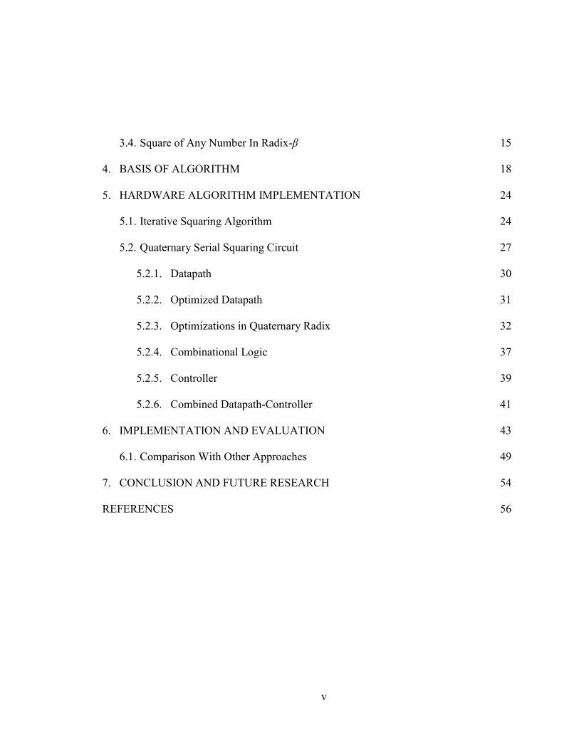
v
3.4. Square of Any Number In Radix-β 15
4. BASIS OF ALGORITHM 18
5. HARDWARE ALGORITHM IMPLEMENTATION 24
5.1. Iterative Squaring Algorithm 24
5.2. Quaternary Serial Squaring Circuit 27
5.2.1. Datapath 30
5.2.2. Optimized Datapath 31
5.2.3. Optimizations in Quaternary Radix 32
5.2.4. Combinational Logic 37
5.2.5. Controller 39
5.2.6. Combined Datapath-Controller 41
6. IMPLEMENTATION AND EVALUATION 43
6.1. Comparison With Other Approaches 49
7. CONCLUSION AND FUTURE RESEARCH 54
REFERENCES 56
vi
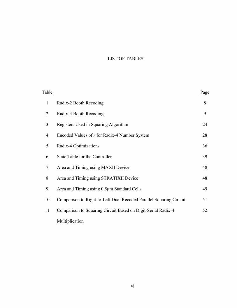
LIST OF TABLES
Table Page
1 Radix-2 Booth Recoding 8
2 Radix-4 Booth Recoding 9
3 Registers Used in Squaring Algorithm 24
4 Encoded Values of r for Radix-4 Number System 28
5 Radix-4 Optimizations 36
6 State Table for the Controller 39
7 Area and Timing using MAXII Device 48
8 Area and Timing using STRATIXII Device 48
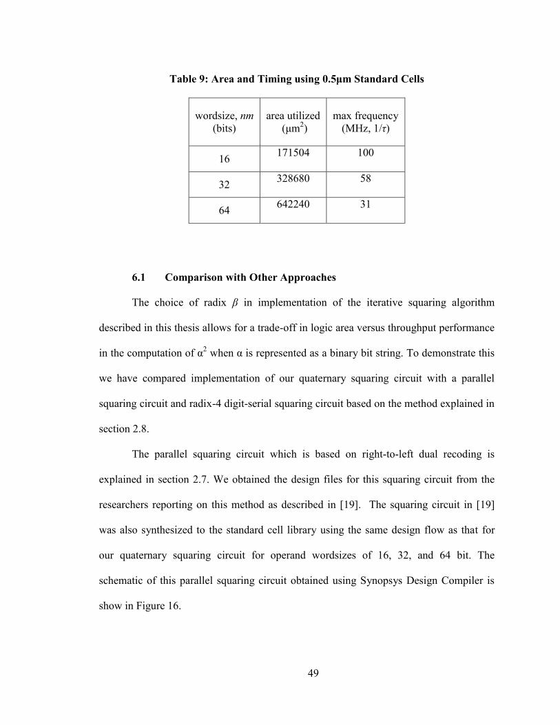
9 Area and Timing using 0.5μm Standard Cells 49
10 Comparison to Right-to-Left Dual Recoded Parallel Squaring Circuit 51
11 Comparison to Squaring Circuit Based on Digit-Serial Radix-4
Multiplication
52
vii
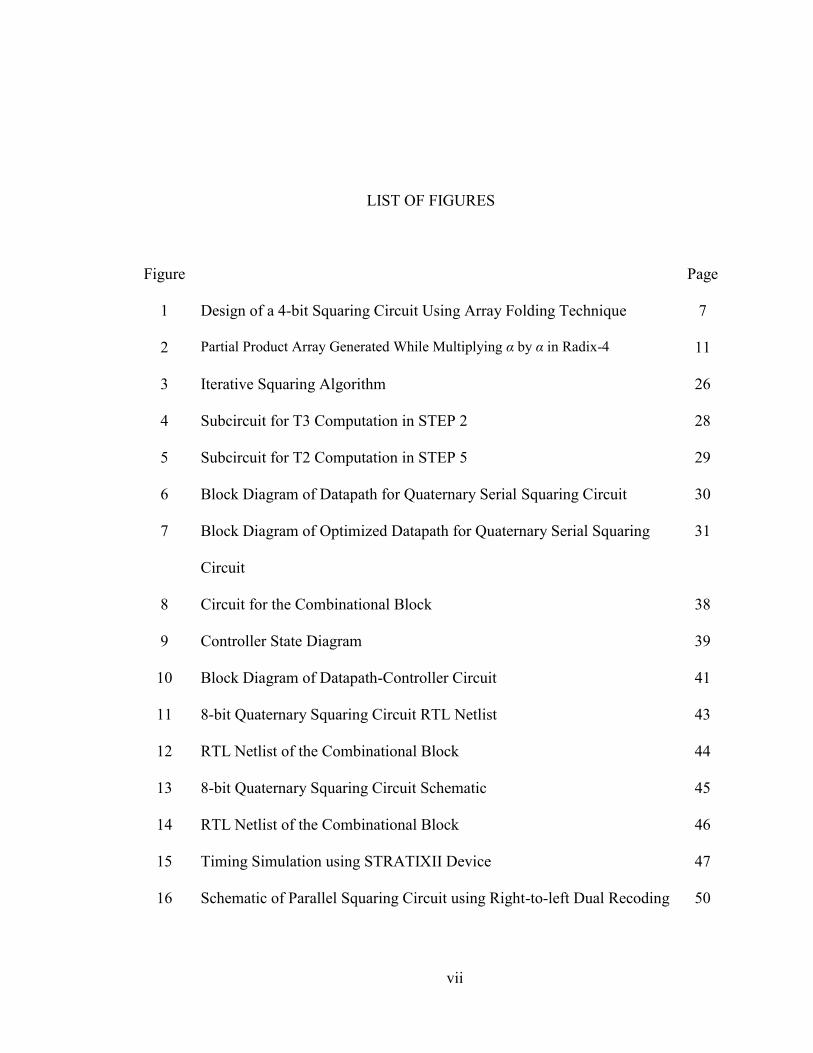
LIST OF FIGURES
Figure Page
1 Design of a 4-bit Squaring Circuit Using Array Folding Technique 7
2 Partial Product Array Generated While Multiplying α by α in Radix-4 11
3 Iterative Squaring Algorithm 26
4 Subcircuit for T3 Computation in STEP 2 28
5 Subcircuit for T2 Computation in STEP 5 29
6 Block Diagram of Datapath for Quaternary Serial Squaring Circuit 30
7 Block Diagram of Optimized Datapath for Quaternary Serial Squaring
Circuit
31
8 Circuit for the Combinational Block 38
9 Controller State Diagram 39
10 Block Diagram of Datapath-Controller Circuit 41
11 8-bit Quaternary Squaring Circuit RTL Netlist 43
12 RTL Netlist of the Combinational Block 44
13 8-bit Quaternary Squaring Circuit Schematic 45
14 RTL Netlist of the Combinational Block 46
15 Timing Simulation using STRATIXII Device 47
16 Schematic of Parallel Squaring Circuit using Right-to-left Dual Recoding 50

viii
17 Schematic of Squaring Circuit Based on Digit-Serial Radix-4 Multiplication 51

ix
ACKNOWLEDGEMENTS
I would like to express my gratitude and love to my family and friends for their
encouragement and constant support throughout the process. I would like express my
deepest appreciation to my advisor, Professor Dr. Mitch Thornton, for giving me an
opportunity to work on a very interesting area of digital circuit design and for his
guidance and support. I would also like to thank members of the Hardware Security
Group in SMU: Dr. Jennifer Dworak, Dr. Theodore Manikas and fellow students, for
their suggestions and valuable discussions. I am thankful to Dr. Sukumaran Nair for his
intellectual encouragement and for agreeing to be in the thesis supervisory committee. I
am also thankful to Dr. David Matula and Jason Moore for their valuable discussions and
for providing their parallel squaring circuit designs for comparative analysis.
1
Chapter 1
INTRODUCTION
Squaring is an essential arithmetic operation in many digital systems. Specialized
squaring circuits have been proposed for digital signal processing applications such as
image compression, pattern recognition and others [1]. Squaring is also a common atomic
computation in cryptography algorithms. The increasing demand for cryptography
hardware support in low power, high-speed mobile devices [2] provides motivation to
devise improved hardware squaring circuit designs. Squaring circuit architecture is also
commonly incorporated in graphics processors. Several general purpose multiplier circuit
designs have also been proposed based on squaring of input operands [3,4].
Bit-serial designs have been proposed in [4,5,6,7] based on the algorithm
discussed in [3]. All these designs require 2nm clock cycles to generate a squared result
of 2nm-bit size, where nm is the number of bits in the input operand or “squarand”
denoted as α in this thesis These designs have seen improvements in area and delay but
still have limitations on throughput due to their bit-serial nature.
Bit-parallel architectures such as the one discussed in [14] mostly make use of
Booth encoding, adder trees such as Wallace trees, and binary tree addition. Though this
design method does not suffer from the performance limitation inherent in bit-serial
architectures and can output more than one resultant bit per cycle, a relatively large
2
amount of circuitry is required to provide support for the multi-operand addition used to
accumulate the partial products.
Several bit-parallel designs have been published based on Booth recoding and
Booth folding techniques that use Wallace or Dada trees and Carry-Save Adders for
accumulation of the partial products of the multiplication operation, α×α [9,10,11].
Higher-radix designs with serial right-to-left significant bit recoding of the input operand
have also been proposed [12,13].
In contrast to the exact squaring approaches, designs have also been proposed to
obtain approximate squaring results [8]. Most approximate squaring designs make use of
the fact that generation of α2
can be accomplished through the production of one-half of
the number of partial products as compared to a general multiplication operation [1].
Because the exact result for α2 results in twice the number of bits compared to the
squarand α, some applications do not require full precision and allow for approximate
methods to be utilized thereby increasing performance, power, and area characteristics.
Typically, the most significant bits of the α2 are desired in approximate methods, thus
techniques that produce the most significant bits first are preferred for bit-serial
approximate squaring methods [12]. Approximate methods based on parallel
implementations can result in reduced partial product accumulation trees, however least
significant digit roundings must be accounted for.
This thesis describes an iterative squaring method that produces a 2nm-bit length
result α2 based on an input squarand α of nm-bits in length. The bit-length of α
2 is
expressed as the product of two positive integers (nm) for convenience in the formulation
of our algorithms. The iterative method produces 2m bits of the output α2
during each
3
intermediate operation. By considering an m-bit grouping within the squarand α as
representing a single radix-2m digit, the circuit can be considered a digit-serial
implementation that produces two m-bit digits per iteration. However, the method as
formulated here is general and does not require the radix to be a power of two. This
generalization allows flexibility in that the approach is applicable for any technology
capable of supporting digit representations over an arbitrary-radix number system.
The method devised in this thesis may be implemented in either software or
hardware. In the research described in this thesis, we implemented the method in
hardware and we thus refer to the implementation as a circuit. This formulation of a
digit-serial architecture allows for a tradeoff between bit-serial and bit-parallel
architectures by allowing for the digit to be represented by m bits. Because 2m bits of the
result are computed in each iterative step, varying m can yield more or less parallelism
while inversely affecting required circuit area and directly affecting throughput. Thus, a
minimal area circuit can be realized when m is small and a large parallel circuit results at
the other extreme when m is set to the wordsize of the squarand. Furthermore, the
iterative nature of the implementation provides a natural means for implementing
pipelining to increase the underlying circuit clock frequency. It is envisioned that
designers will choose an appropriate value of m such that the performance requirements
are met while minimizing the amount of circuitry required.
Arithmetically, the technique assumes the squarand is represented as a higher-
radix digit string where each digit is represented by an m-bit substring. Furthermore, the

4
technique yields two digits of the output squared value during each iterative step; hence,
a total of 2m bits of the squared result are computed at each iterative step.
5
Chapter 2
BACKGROUND
2.1 Fixed-Radix Positional Number Systems
The fixed-radix, fixed-point number systems utilized in this work are based on a
positive integer radix-β such that β ≥ 2. The ‘radix polynomial’ form of a value α is
written as a (p+q) term polynomial of the form [15]:
In the above ‘radix-polynomial’ the p-terms form the whole part of the integer
value α and the q-terms form the fractional part. In the work presented here, we assume
the squarand is a fixed-point value with arbitrary placement of the radix-point. Hence,
the radix-polynomial is simplified and written as a general m-term polynomial as follows.
Since here we are designing a squaring circuit for fixed point numbers for the
purpose of simplifying proofs and examples, we use the radix-polynomial form of a value
α as an n-term polynomial given below:
The squarand α can also be represented in a radix-β number system in the form of
a positional string of m characters denoted by α=[ɑm-1ɑm-2 … ɑ2ɑ1ɑ0]β where each digit ɑi
is the radix-polynomial coefficient and the subscript β indicates the particular radix. For
clarity, the character strings denoting the positional digit representation of the value α
6
may be enclosed by square brackets. The digits ɑi are the coefficients of the radix-
polynomial form and their position within the string inherently denotes the exponent of
the radix β. Additionally, digit strings and other values are sometimes subscripted by the
radix β of the particular number system being used, α=[ɑm-1ɑm-2 … ɑ2ɑ1ɑ0]β.
Each character ɑi in a positional string representing a value is referred to as a
‘digit’ regardless of the radix of the number system. Binary digits may alternatively be
referred to as ‘bits’ in this thesis. For fixed-radix, fixed-radix number systems, digits are
restricted to the natural numbers and are members of the set {ɑi ∈ N|0 ≤ ɑi ≤ β-1}. For the
case where β>1010, single characters are used to represent a digit such as the characters
‘A’ through ‘F’ for the case of β=1610.
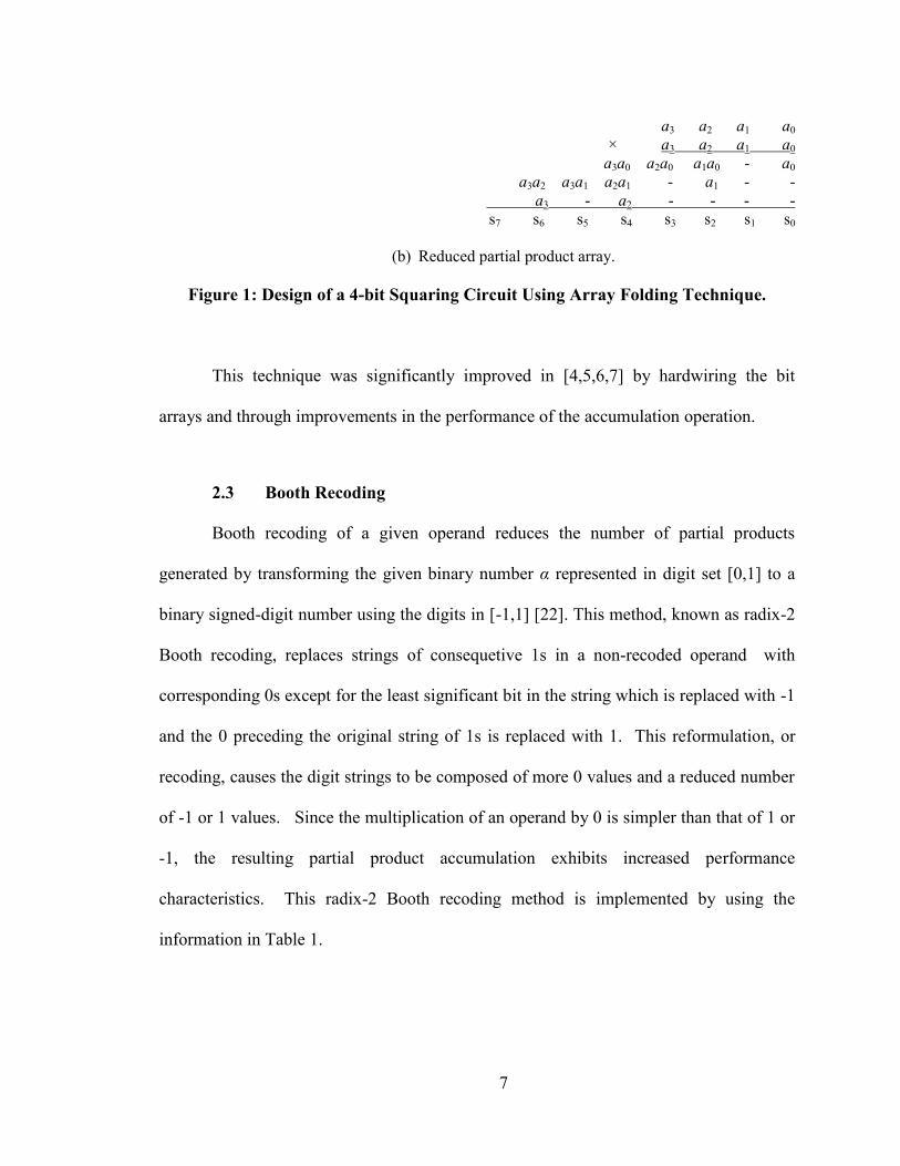
2.2 Array Folding Technique
This method makes use of symmetry in the partial product array generated while
obtaining a square of a number [3,21]. An example of the array-folding technique is
demonstrated in Figure 1 for a 4-bit unsigned binary integer. The basic principle is that
the partial product accumulation is simplified where any term ɑiɑi is reduced to ɑi and any
two terms αiαj and ɑiɑj in the same column is replaced by ɑiɑj in next higher column.
ɑ3 ɑ2 ɑ1 ɑ0
× ɑ3 ɑ2 ɑ1 ɑ0
ɑ3ɑ0 ɑ2ɑ0 ɑ1ɑ0 ɑ0ɑ0
ɑ3ɑ1 ɑ2ɑ1 ɑ1ɑ1 ɑ0ɑ1 -
ɑ3ɑ2 ɑ2ɑ2 ɑ1ɑ2 ɑ0ɑ2 - -
ɑ3ɑ3 ɑ2ɑ3 ɑ1ɑ3 ɑ0ɑ3 - - -
s7 s6 s5 s4 s3 s2 s1 s0
(a) Partial product array generated while multiplying α by α.
7
ɑ3 ɑ2 ɑ1 ɑ0
× ɑ3 ɑ2 ɑ1 ɑ0
ɑ3ɑ0 ɑ2ɑ0 ɑ1ɑ0 - ɑ0
ɑ3ɑ2 ɑ3ɑ1 ɑ2ɑ1 - ɑ1 - -
ɑ3 - ɑ2 - - - -
s7 s6 s5 s4 s3 s2 s1 s0
(b) Reduced partial product array.
Figure 1: Design of a 4-bit Squaring Circuit Using Array Folding Technique.
This technique was significantly improved in [4,5,6,7] by hardwiring the bit
arrays and through improvements in the performance of the accumulation operation.
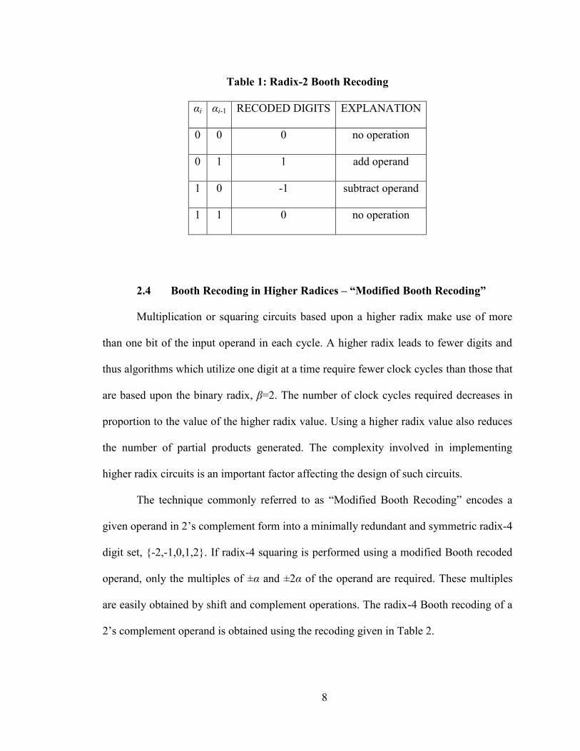
2.3 Booth Recoding
Booth recoding of a given operand reduces the number of partial products
generated by transforming the given binary number α represented in digit set [0,1] to a
binary signed-digit number using the digits in [-1,1] [22]. This method, known as radix-2
Booth recoding, replaces strings of consequetive 1s in a non-recoded operand with
corresponding 0s except for the least significant bit in the string which is replaced with -1
and the 0 preceding the original string of 1s is replaced with 1. This reformulation, or
recoding, causes the digit strings to be composed of more 0 values and a reduced number
of -1 or 1 values. Since the multiplication of an operand by 0 is simpler than that of 1 or
-1, the resulting partial product accumulation exhibits increased performance
characteristics. This radix-2 Booth recoding method is implemented by using the
information in Table 1.
8
Table 1: Radix-2 Booth Recoding
αi αi-1 RECODED DIGITS EXPLANATION
0 0 0 no operation
0 1 1 add operand
1 0 -1 subtract operand
1 1 0 no operation
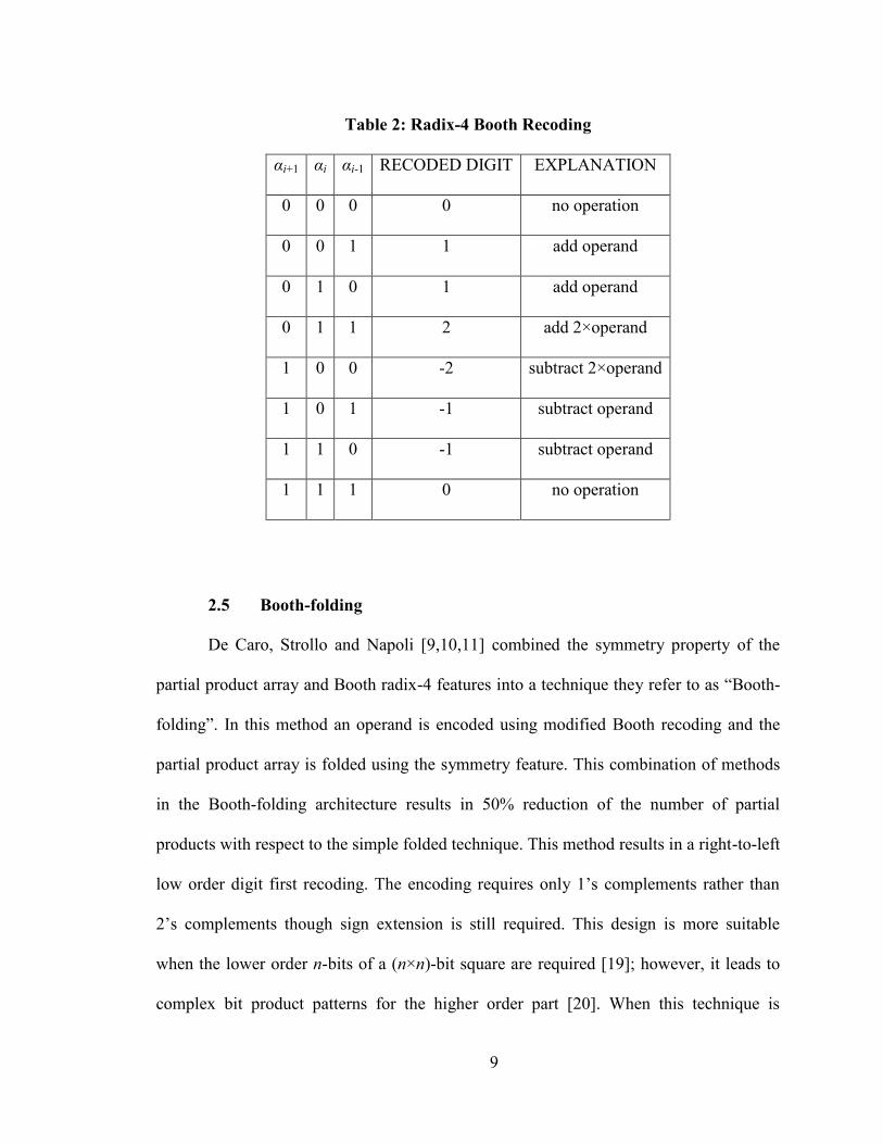
2.4 Booth Recoding in Higher Radices – “Modified Booth Recoding”
Multiplication or squaring circuits based upon a higher radix make use of more
than one bit of the input operand in each cycle. A higher radix leads to fewer digits and
thus algorithms which utilize one digit at a time require fewer clock cycles than those that
are based upon the binary radix, β=2. The number of clock cycles required decreases in
proportion to the value of the higher radix value. Using a higher radix value also reduces
the number of partial products generated. The complexity involved in implementing
higher radix circuits is an important factor affecting the design of such circuits.
The technique commonly referred to as “Modified Booth Recoding” encodes a
given operand in 2’s complement form into a minimally redundant and symmetric radix-4
digit set, {-2,-1,0,1,2}. If radix-4 squaring is performed using a modified Booth recoded
operand, only the multiples of ±α and ±2α of the operand are required. These multiples
are easily obtained by shift and complement operations. The radix-4 Booth recoding of a
2’s complement operand is obtained using the recoding given in Table 2.
9
Table 2: Radix-4 Booth Recoding
αi+1 αi αi-1 RECODED DIGIT EXPLANATION
0 0 0 0 no operation
0 0 1 1 add operand
0 1 0 1 add operand
0 1 1 2 add 2×operand
1 0 0 -2 subtract 2×operand
1 0 1 -1 subtract operand
1 1 0 -1 subtract operand
1 1 1 0 no operation
2.5 Booth-folding
De Caro, Strollo and Napoli [9,10,11] combined the symmetry property of the
partial product array and Booth radix-4 features into a technique they refer to as “Booth-
folding”. In this method an operand is encoded using modified Booth recoding and the
partial product array is folded using the symmetry feature. This combination of methods
in the Booth-folding architecture results in 50% reduction of the number of partial
products with respect to the simple folded technique. This method results in a right-to-left
low order digit first recoding. The encoding requires only 1’s complements rather than
2’s complements though sign extension is still required. This design is more suitable
when the lower order n-bits of a (n×n)-bit square are required [19]; however, it leads to
complex bit product patterns for the higher order part [20]. When this technique is
10
extended to radix-8 it requires computation of factors that are multiples of three that
further increase complexity since logic is required in addition to the shift and
complement operations needed for the radix-4 approach.
2.6 Left-to-right Dual Recoding
Another technique is proposed in [12] that employs left-to-right leading digit-first
dual recoding and provides several features not available as compared to the right-to-left
Booth-folding encoding method. Left-to-right recoding is applicable to both radix-4 and
radix-8 such that it results in partial square generators similar in design to Booth radix-4
and radix-8 recoded partial product generators, but only requiring one-half the size of a
comparable multiplier’s partial product array. The partial squares generated are all non-
negative, so no sign extensions are needed as compared to the previous right-to-left
Booth-folding technique. The squarand digits are identical to Booth recoded digits for
radix-4 and radix-8.
2.7 Right-to-left Dual Recoding
This technique is similar to the left-to-right dual recoding technique described in
the previous section. Sign extensions are required in this technique since the generated
partial squares may be negative. In a later chapter of this thesis, we use the radix-4
implementation of the squaring circuit based on this technique as described in [19] for
comparison with the performance of our proposed squaring circuit in radix-4.
11
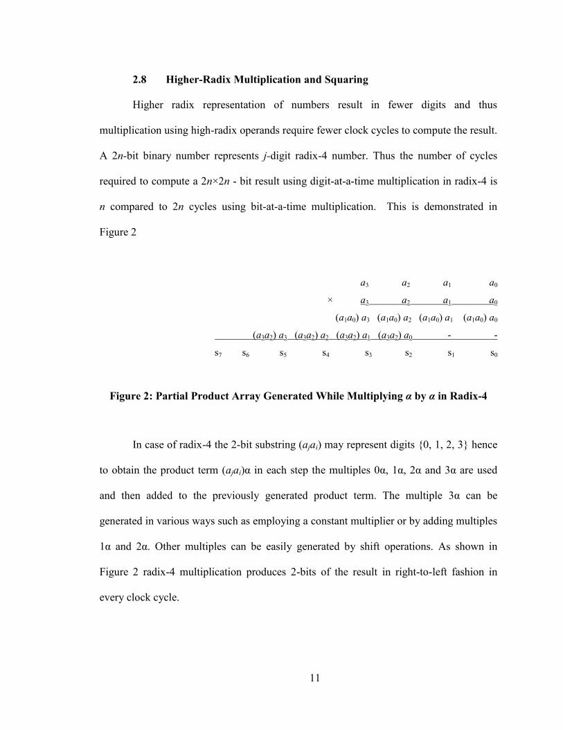
2.8 Higher-Radix Multiplication and Squaring
Higher radix representation of numbers result in fewer digits and thus
multiplication using high-radix operands require fewer clock cycles to compute the result.
A 2n-bit binary number represents j-digit radix-4 number. Thus the number of cycles
required to compute a 2n×2n - bit result using digit-at-a-time multiplication in radix-4 is
n compared to 2n cycles using bit-at-a-time multiplication. This is demonstrated in
Figure 2
ɑ3 ɑ2 ɑ1 ɑ0
× ɑ3 ɑ2 ɑ1 ɑ0
(ɑ1ɑ0) ɑ3 (ɑ1ɑ0) ɑ2 (ɑ1ɑ0) ɑ1 (ɑ1ɑ0) ɑ0
(ɑ3ɑ2) ɑ3 (ɑ3ɑ2) ɑ2 (ɑ3ɑ2) ɑ1 (ɑ3ɑ2) ɑ0 - -
s7 s6 s5 s4 s3 s2 s1 s0
Figure 2: Partial Product Array Generated While Multiplying α by α in Radix-4
In case of radix-4 the 2-bit substring (ɑjɑi) may represent digits {0, 1, 2, 3} hence
to obtain the product term (ɑjɑi)α in each step the multiples 0α, 1α, 2α and 3α are used
and then added to the previously generated product term. The multiple 3α can be
generated in various ways such as employing a constant multiplier or by adding multiples
1α and 2α. Other multiples can be easily generated by shift operations. As shown in
Figure 2 radix-4 multiplication produces 2-bits of the result in right-to-left fashion in
every clock cycle.
12
Chapter 3
THEORY OF APPROACH
3.1 Notation
The following additional notation is used in the description of our digit-serial
fixed-point squaring algorithm.
LSD(α,k) and MSD(α,k) are operators that yield the k least significant or most
significant digits in the digit string representing a value α. LSD(α,1)
represents the least significant digit of α, LSD(α,1)=ɑ0. Likewise the most
significant digit is given as MSD(α,1)=ɑn-1.
{A,B,C} denotes concatenation of the content of registers A, B and C that can
be of any size and whose individual sizes may differ.
SHL(A,k,B) denotes the operation of shifting the content of register A to the
left by k bits and setting the least significant k bits to the content of register B.
A can be of any size greater than or equal to the size of B and B must be of
size k.
SHR(A,k,B) denotes the operation of shifting the content of register A to the
right by k bits and setting the most significant k bits of A to the content of
13
register B. A can be of any size greater than or equal to the size of B and B
must be of size k.
A←B denotes the operation of setting the content of register A with that of
register B. Registers A and B must be of the same size.
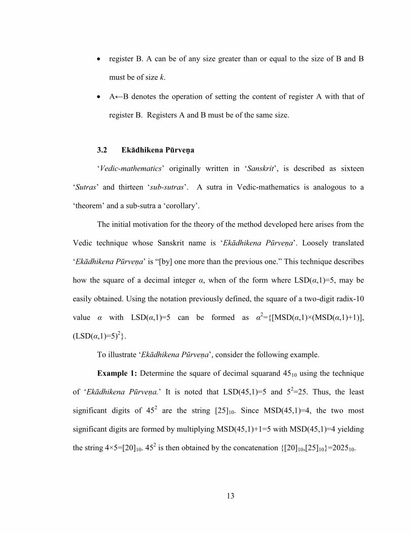
3.2 Ekādhikena Pūrveṇa
‘Vedic-mathematics’ originally written in ‘Sanskrit’, is described as sixteen
‘Sutras’ and thirteen ‘sub-sutras’. A sutra in Vedic-mathematics is analogous to a
‘theorem’ and a sub-sutra a ‘corollary’.
The initial motivation for the theory of the method developed here arises from the
Vedic technique whose Sanskrit name is ‘Ekādhikena Pūrveṇa’. Loosely translated
‘Ekādhikena Pūrveṇa’ is “[by] one more than the previous one.” This technique describes
how the square of a decimal integer α, when of the form where LSD(α,1)=5, may be
easily obtained. Using the notation previously defined, the square of a two-digit radix-10
value α with LSD(α,1)=5 can be formed as α2={[MSD(α,1)×(MSD(α,1)+1)],
(LSD(α,1)=5)2}.
To illustrate ‘Ekādhikena Pūrveṇa’, consider the following example.
Example 1: Determine the square of decimal squarand 4510 using the technique
of ‘Ekādhikena Pūrveṇa.’ It is noted that LSD(45,1)=5 and 52=25. Thus, the least
significant digits of 452 are the string [25]10. Since MSD(45,1)=4, the two most
significant digits are formed by multiplying MSD(45,1)+1=5 with MSD(45,1)=4 yielding
the string 4×5=[20]10. 452 is then obtained by the concatenation {[20]10,[25]10}=202510.
14
While the method is very interesting, it is limited to cases where the squarand is a
radix-10 value with the least significant digit happening to be exactly one-half of the
radix value, 10/2=5.
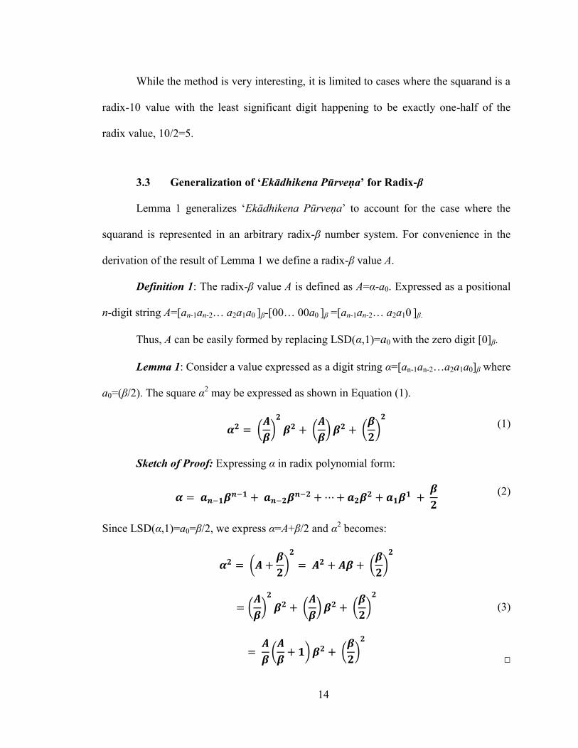
3.3 Generalization of ‘Ekādhikena Pūrveṇa’ for Radix-β
Lemma 1 generalizes ‘Ekādhikena Pūrveṇa’ to account for the case where the
squarand is represented in an arbitrary radix-β number system. For convenience in the
derivation of the result of Lemma 1 we define a radix-β value A.
Definition 1: The radix-β value A is defined as A=α-ɑ0. Expressed as a positional
n-digit string A=[ɑn-1ɑn-2… ɑ2ɑ1ɑ0 ]β-[00… 00ɑ0 ]β =[ɑn-1ɑn-2… ɑ2ɑ10 ]β.
Thus, A can be easily formed by replacing LSD(α,1)=ɑ0 with the zero digit [0]β.
Lemma 1: Consider a value expressed as a digit string α=[ɑn-1ɑn-2…ɑ2ɑ1ɑ0]β where
ɑ0=(β/2). The square α2 may be expressed as shown in Equation (1).
(
)
(
) (
)
(1)
Sketch of Proof: Expressing α in radix polynomial form:
(2)
Since LSD(α,1)=ɑ0=β/2, we express α=A+β/2 and α2 becomes:
(
)
(
)
(
)
(
) (
)
(
) (
)
(3)
□
15
The result of Lemma 1 can be used as the basis of a squaring algorithm where the
second two terms of the right-hand side of Equation (1) are calculated in each iterative
step, the first term is used for subsequent iterations, and the results are accumulated at
each step. The algorithm clearly converges since subsequent iterative steps use an
operand with two fewer digits in the digit string representation. The β2 factor in the first
term is accounted for by implementing a shifting operation during the accumulation step.
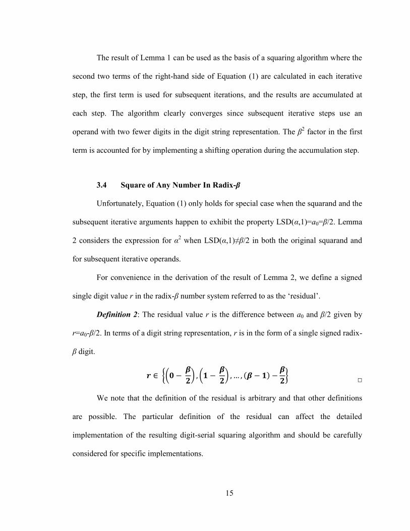
3.4 Square of Any Number In Radix-β
Unfortunately, Equation (1) only holds for special case when the squarand and the
subsequent iterative arguments happen to exhibit the property LSD(α,1)=ɑ0=β/2. Lemma
2 considers the expression for α2 when LSD(α,1)≠β/2 in both the original squarand and
for subsequent iterative operands.
For convenience in the derivation of the result of Lemma 2, we define a signed
single digit value r in the radix-β number system referred to as the ‘residual’.
Definition 2: The residual value r is the difference between ɑ0 and β/2 given by
r=ɑ0-β/2. In terms of a digit string representation, r is in the form of a single signed radix-
β digit.
∈ {(
) (
) ( )
}
□
We note that the definition of the residual is arbitrary and that other definitions
are possible. The particular definition of the residual can affect the detailed
implementation of the resulting digit-serial squaring algorithm and should be carefully
considered for specific implementations.
16
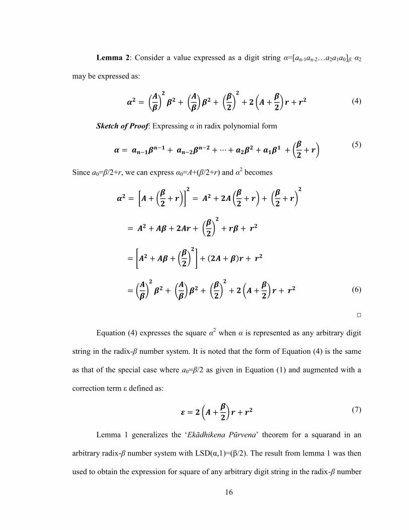
Lemma 2: Consider a value expressed as a digit string α=[ɑn-1ɑn-2…ɑ2ɑ1ɑ0]β. α2
may be expressed as:
(
)
(
) (
)
(
) (4)
Sketch of Proof: Expressing α in radix polynomial form
(
)
(5)
Since ɑ0=β/2+r, we can express α0=A+(β/2+r) and α2 becomes
[ (
)]
(
) (
)
(
)
[ (
)
] ( )
(
)
(
) (
)
(
) (6)
□
Equation (4) expresses the square α2 when α is represented as any arbitrary digit
string in the radix-β number system. It is noted that the form of Equation (4) is the same
as that of the special case where ɑ0=β/2 as given in Equation (1) and augmented with a
correction term ε defined as:
(
) (7)
Lemma 1 generalizes the ‘Ekādhikena Pūrvena’ theorem for a squarand in an
arbitrary radix-β number system with LSD(α,1)=(β/2). The result from lemma 1 was then
used to obtain the expression for square of any arbitrary digit string in the radix-β number

17
system. This expression forms the basis of our iterative squaring algorithm which is
described in next chapter.
18
Chapter 4
BASIS OF ALGORITHM
Equation (4) and previous definitions may be used to formulate a digit-serial
squaring algorithm. The motivation for formulating this algorithm is that the choice of
radix-β allows for a trade-off in logic circuit area versus throughput performance in the
computation of a α2 when α is represented as a binary bit string. Higher values of β allow
more bits to be produced per iterative step in the resulting representation of α2. The area
versus performance tradeoff occurs in that the amount of computation or logic circuitry
required at each iterative step increases for higher radix values.
In the basis of the algorithm as stated here, we assume that the squarand is of the
form of a binary bit string. Intermediate computations can be efficiently implemented
when we restrict the radix β to be of the form β=2m where m is a positive integer m≥2.
Efficiency results since β=2m allows each higher radix digit in the string representing α to
be equivalent to an m-bit substring within α. α, in terms of a higher-radix digit string, is
simply the concatenation of the disjoint m-bit substrings of α in binary form where
LSD(α,1) is represented by the least significant m-bits, the subsequent next significant
higher-radix digit is represented by the next group of m bits to the left of LSD(α,1), and
so on.
It is noted that the results of Lemmas 1 and 2 hold for any general radix value and
that the restriction of β=2m is only used for convenience in formulating the squaring
19
algorithm when squarands are given as a binary bit string. This case is of particular
interest in our implementation since we are targeting computer arithmetic circuits and
algorithms implemented with binary switching logic. Future technologies may employ
non-binary switching elements [16] and the technique developed in this paper is equally
applicable for such non-binary technologies.
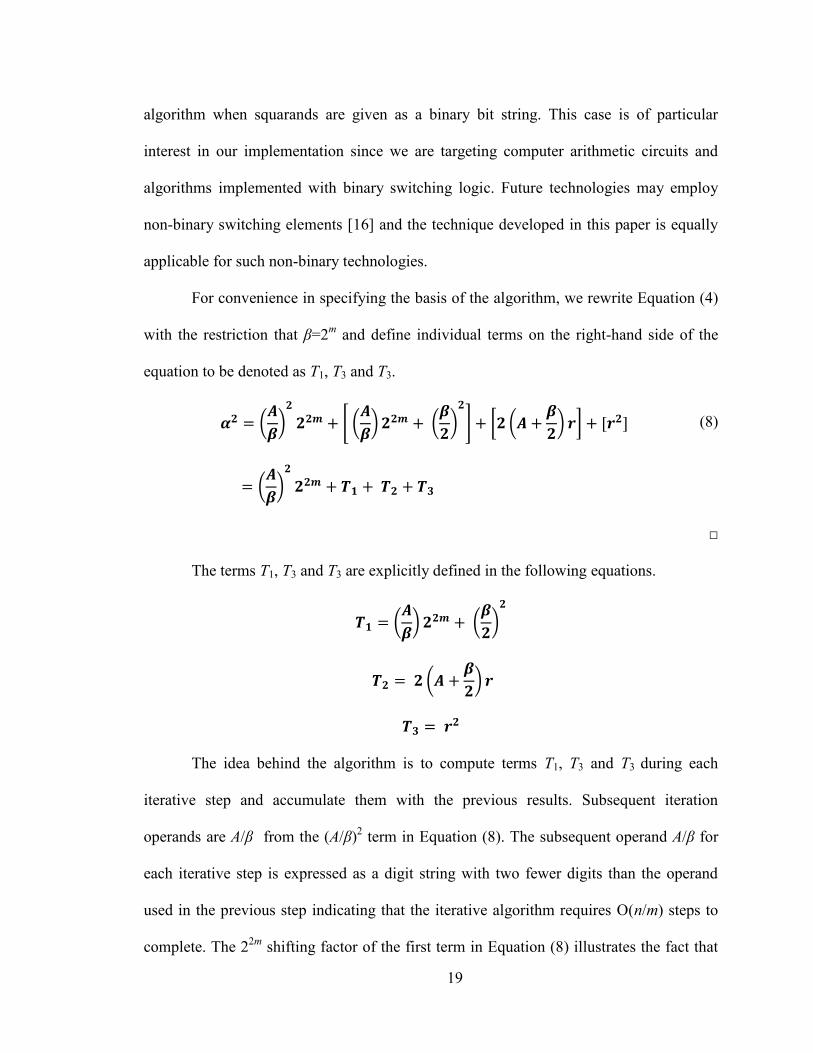
For convenience in specifying the basis of the algorithm, we rewrite Equation (4)
with the restriction that β=2m and define individual terms on the right-hand side of the
equation to be denoted as T1, T3 and T3.
(
)
[ (
) (
)
] [ (
) ] (8)
(
)
□
The terms T1, T3 and T3 are explicitly defined in the following equations.
(
) (
)
(
)
The idea behind the algorithm is to compute terms T1, T3 and T3 during each
iterative step and accumulate them with the previous results. Subsequent iteration
operands are A/β from the (A/β)2 term in Equation (8). The subsequent operand A/β for
each iterative step is expressed as a digit string with two fewer digits than the operand
used in the previous step indicating that the iterative algorithm requires O(n/m) steps to
complete. The 22m
shifting factor of the first term in Equation (8) illustrates the fact that
20
two high-radix digits (2m length bitstrings) are produced at each step and that they
represent two independent digits in the final result of α2. The resulting digits in α
2 are
produced in the order of the lesser significant digits first (right-to-left fashion).
Before stating the algorithm in RTL form, several observations are noted and used
to more efficiently implement the computation of the three terms T1, T2 and T3.
Observation 1: The term A/β is efficiently obtained by shifting the digit string
representing α one position to the right and discarding ɑ0, A/β=[ɑn-1ɑn-2… ɑ2ɑ1]β □
Observation 2: Values that are multiplied by a factor of β=2km
may be easily
obtained by shifting the value left by km bit positions and inserting a radix-β zero digit
place holder [0]β for the vacated least significant digits. □
Observation 3: The term β/2 is always of the form of a single radix-β digit
expressed as an m-bit binary string, β/2=[10..0]2. □
Observation 4: The term (β/2)2 is always of the form of two radix-β digits with
the most significant digit of value β/4 and the least significant digit [q1q0]β, with the most
significant digit of value q1=MSD((β/2)2,1)=β/4=[010..0]2 and the least significant digit
of value q0=LSD((β/2)2,1)=0=[0…0]2. Hence, expressed as a 2m-bit binary string,
(β/2)2={[010…0]2, [000…0]2}. □
Term T1 is computed in a single operation. Making use of Observations 1 and 2,
the value (A/β)22m
is obtained by forming the digit string [ɑn-1ɑn-2… ɑ2ɑ100 ]β.
Furthermore by Observation 4, (β/2)2 can always be expressed as two radix-2
m digits (2m
bits) denoted as [q1q0]β. Thus, T1 is obtained by forming the string [ɑn-1ɑn-2…ɑ2ɑ1q1q0]β.
From Observation 4, q1=β/4 and q0=0 so that (β/2)2=[ q1q0]β=[(β/4)0]β. Thus, the digit
string representation for T1 is [ɑn-1ɑn-2… ɑ2ɑ1(β/4)0 ]β.
21
Term T2 is computed by first forming a digit string representing 2(A+β/2) and
then multiplying this string with the single radix-β digit b. Using Observations 1, 2, and
3, A=[ɑn-1ɑn-2… ɑ2ɑ1 q1q0]β and β/2 is always represented as a single unsigned radix-2m
digit (m-bit string). Therefore, (A+β/2)=[ɑn-1ɑn-2… ɑ2ɑ1 (β/2)]. To account for the
multiplicative factor of 2, the (A+β/2)=[ɑn-1ɑn-2… ɑ2ɑ1 (β/2)]β digit string is shifted by one
bit position to the left resulting in 2(A+β/2). We note that the multiplicative factor 2
would in general need to be implemented through the use of an addition operation,
2(A+β/2)= (A+β/2)+(A+β/2), when a higher-valued radix-β is used that is not an integral
power of two since this can be considered a ‘fractional digit shift’.
The final step in the formation of term T2 involves the multiplication of
2(A+β/2)=[ɑn-1ɑn-2… ɑ2ɑ1 (β/2)]β by the signed single radix-2m digit b=ɑ0-β/2. Because r
is a single digit value, this multiplication can be accomplished with a minimal amount of
computation or circuitry as compared to a general-purpose multiply operation or circuit.
Clearly, as the value m is increased resulting in a higher-valued radix, 2m, both
computational complexity and overall algorithm throughput increases. The actual
implementation of the multiplication by b is dependent upon the value m and should be
carefully considered for a given realization of the algorithm. Relatively small values of m
generally allow for a simple logic circuit or a lookup table to be used.
The final step in the formation of term T3=r2
requires the computation of the
square of the residual value b. The implementation of this computation is also dependent
upon the size of m, which dictates the number of bits required to represent a radix-2m
digit. For smaller values of m, the direct calculation of r2 can be very efficiently
implemented as a small combinational logic circuit or lookup table. As m increases, the
22
computation of b2 becomes more complex and other methods may be employed. We note
that even for large values of m, the computation of T3=b2 can be accomplished in parallel
with the computation of the other terms T1 and T2 since accumulation of T1+T2+T3 with
overall result can occur at the end of each iterative step.
After terms T1, T2 and T3 are formulated; they are summed together and
accumulated with the previous result. The accumulation takes into account the process of
multiplying subsequent iterative operands by 22m
and the fact that two independent radix-
β digits (or, 2m-bits) of the final result are produced at each iterative step. This can be
implemented in a variety of ways. We choose to initialize a final result register to zero.
The size of the register is 2nm-bits where n is the number of radix-β digits representing ɑ
and m denotes the radix. The final operation of each iterative step of the algorithm is to
shift the result register 2m bits to the right and insert the 2m least significant bits of
T1+T2+T3 into the most significant positions of the shifted result register. Insertion of the
two radix-2m digits in the most significant portion of the result register instead of
performing a multi-bit left shift before adding them to the previously accumulated result
allows the algorithm to be implemented without the need for an inclusion of a multi-bit
left shift operation or the use of a barrel shifting circuit in a hardware realization. This is
an important aspect of the accumulation process since a multi-bit left-shift operation is
considerably more complex as compared to a fixed length (2m bit) right-shift operation
The algorithm uses an iterative index i to determine if all digits of the squarand
have been produced. For an n-digit radix-β squarand, the squared result consists of 2n
digits. Since two digits are produced per iterative step, index i ranges from zero to (n/2)-
1. Initially, when i=0, ɑ is the original squarand. During intermediate computations, when
23
0<i< n/2, the algorithm iterates and sets the intermediate squarand to α=A/β. In the final
iterative step, the squarand argument becomes α=0, however this step is required since
the residual b may not be zero-valued.
Any given implementation of the algorithm should include careful consideration
of the manner in which the signed digit r is represented. When r is represented using a
radix-complement or a signed-magnitude form, m+1 bits are needed to account for the
sign. Furthermore, depending upon the definition of the residual, r can take on integer
values in either of the ranges [-(β/2),(β/2-1)] (as is the case in this formulation) or [-
(β/2)+1,(β/2)]. However, since there is a one-to-one relationship between a0 and r (since
r=a0-β/2), we use the m-bit string representing a0 to represent the corresponding r value
thus allowing r to be encoded as an m-bit string.
Using the expressions for terms T1, T2, T3 and the observations previously stated
in this chapter we can formulate an iterative squaring algorithm for hardware
implementation of squaring circuit. This iterative squaring algorithm is stated in next
chapter followed by description of implementation of squaring circuit based on this
iterative algorithm.
24
Chapter 5
HARDWARE ALGORITHM IMPLEMENTATION
5.1 Iterative Squaring Algorithm
The algorithm formulated in the previous chapter makes use of several registers.
For succinctness, we define the registers used within the statement of the algorithm in
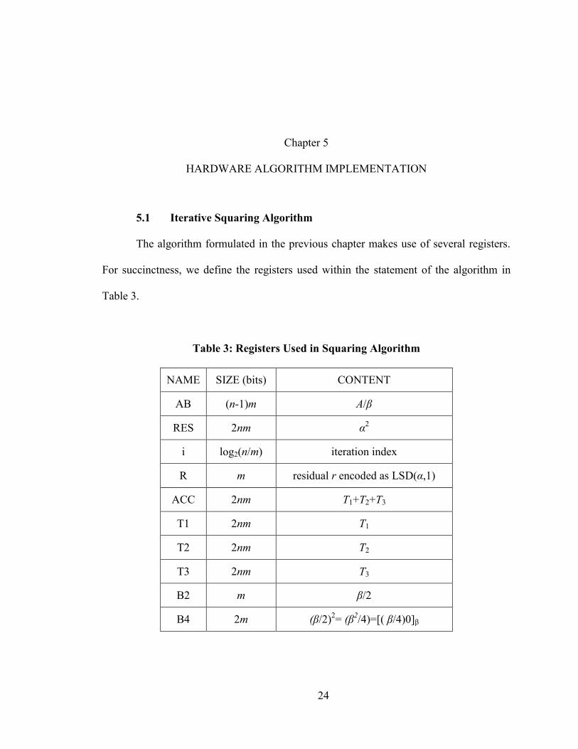
Table 3.
Table 3: Registers Used in Squaring Algorithm
NAME SIZE (bits) CONTENT
AB (n-1)m A/β
RES 2nm α2
i log2(n/m) iteration index
R m residual r encoded as LSD(α,1)
ACC 2nm T1+T2+T3
T1 2nm T1
T2 2nm T2
T3 2nm T3
B2 m β/2
B4 2m (β/2)2= (β
2/4)=[( β/4)0]β
25
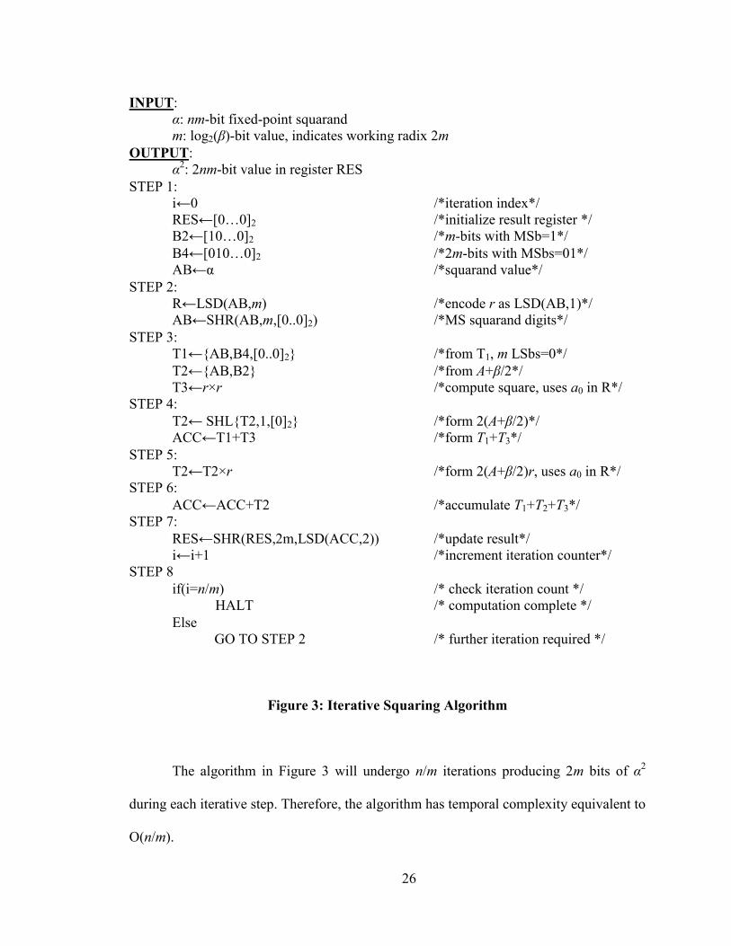
A register transfer level (RTL) statement of the algorithm is given in Figure 3.
Intermediate locations within the algorithm statement are denoted by labels in the form of
‘STEP k’. The labels are included for convenience in referring to certain portions of the
algorithm and they also indicate clock boundaries in that the results of STEP k-1 are
registered before computation occurs in STEP k. As an example, the T2←{AB,B2}
operation of STEP 3 must complete before the T2←SHL{T2,1,[0]2} operation of STEP 4
can proceed. Breaking up the computation of term T2 into multiple intermediate registered
operations is an example of pipelining the datapath and allows for the overall circuit
clock speed to be increased in a hardware realization of the algorithm.
26
INPUT:
α: nm-bit fixed-point squarand
m: log2(β)-bit value, indicates working radix 2m
OUTPUT:
α2: 2nm-bit value in register RES
STEP 1:
i←0 /*iteration index*/
RES←[0…0]2 /*initialize result register */
B2←[10…0]2 /*m-bits with MSb=1*/
B4←[010…0]2 /*2m-bits with MSbs=01*/
AB←α /*squarand value*/
STEP 2:
R←LSD(AB,m) /*encode r as LSD(AB,1)*/
AB←SHR(AB,m,[0..0]2) /*MS squarand digits*/
STEP 3:
T1←{AB,B4,[0..0]2} /*from T1, m LSbs=0*/
T2←{AB,B2} /*from A+β/2*/
T3←r×r /*compute square, uses a0 in R*/
STEP 4:
T2← SHL{T2,1,[0]2} /*form 2(A+β/2)*/
ACC←T1+T3 /*form T1+T3*/
STEP 5:
T2←T2×r /*form 2(A+β/2)r, uses a0 in R*/
STEP 6:
ACC←ACC+T2 /*accumulate T1+T2+T3*/
STEP 7:
RES←SHR(RES,2m,LSD(ACC,2)) /*update result*/
i←i+1 /*increment iteration counter*/
STEP 8
if(i=n/m) /* check iteration count */
HALT /* computation complete */
Else
GO TO STEP 2
/* further iteration required */
Figure 3: Iterative Squaring Algorithm
The algorithm in Figure 3 will undergo n/m iterations producing 2m bits of α2
during each iterative step. Therefore, the algorithm has temporal complexity equivalent to
O(n/m).
27
In terms of required computational resources, the algorithm requires
circuitry to perform shifting, bit-string concatenation, and m-bit operand squaring. While
(nm+m)-bit and (nm+m+1)-bit operand addition is required in STEPs 4 and 6, it is noted
that a single (nm+m+1)-bit addition circuit can be used since these sums may be formed
sequentially allowing for reuse of a single (nm+m+1)-bit adder. The multiplication and
single-digit squaring operations can be implemented in a variety of forms although it is
noted that due to the relatively small size of the operands (m-bits) very compact and fast
circuits such as lookup tables are a practical choice. With respect to throughput, the
algorithm requires n/m iterations producing 2m bits of α2
during each iterative step.
Therefore, the algorithm has temporal complexity equivalent to O(n/m).
5.2 Quaternary Serial Squaring Circuit
To demonstrate and evaluate the digit-serial squaring algorithm, we designed and
implemented a synchronous digital logic circuit using a quaternary radix, β=22=4. This
choice of radix allows for comparison to other squaring circuits based on radix-4 Booth
recoding and provides an intermediate solution between bit-serial and bit-parallel
realizations. The circuit architecture is of the form of a clocked synchronous controller
with a corresponding datapath subcircuit that implements the operations specified in the
algorithm.
The computation of T3←r×r in STEP3 uses a multiplexer based lookup structure.
A 4:1 multiplexer with 2m-bit data paths and an m-bit control signal chooses among the
appropriate squared values or r. The squared values of r2 that drive the multiplexer data
inputs are pre-computed before implementation of the circuitry and are either hardwired
28
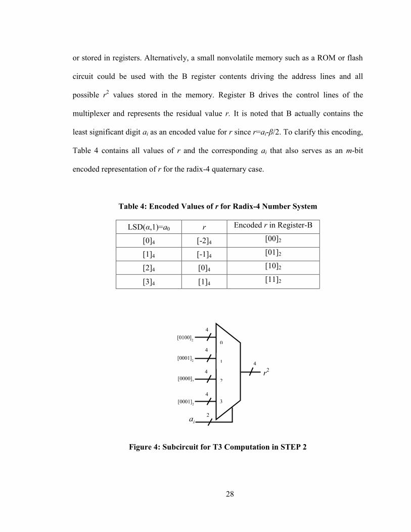
or stored in registers. Alternatively, a small nonvolatile memory such as a ROM or flash
circuit could be used with the B register contents driving the address lines and all
possible r2 values stored in the memory. Register B drives the control lines of the
multiplexer and represents the residual value r. It is noted that B actually contains the
least significant digit ai as an encoded value for r since r=ai-β/2. To clarify this encoding,
Table 4 contains all values of r and the corresponding ai that also serves as an m-bit
encoded representation of r for the radix-4 quaternary case.
Table 4: Encoded Values of r for Radix-4 Number System
LSD(α,1)=a0 r Encoded r in Register-B
[0]4 [-2]4 [00]2
[1]4 [-1]4 [01]2
[2]4 [0]4 [10]2
[3]4 [1]4 [11]2
Figure 4: Subcircuit for T3 Computation in STEP 2
ai
2
4
4
4
4
r2
[0100]2
[0001]2
[0000]2
[0001]2
3
0
2
4
1
29
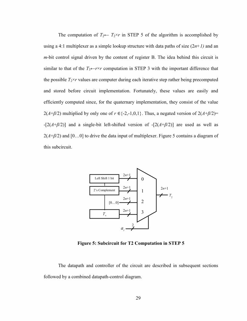
The computation of T2← T2×r in STEP 5 of the algorithm is accomplished by
using a 4:1 multiplexer as a simple lookup structure with data paths of size (2n+1) and an
m-bit control signal driven by the content of register B. The idea behind this circuit is
similar to that of the T3←r×r computation in STEP 3 with the important difference that
the possible T2×r values are computer during each iterative step rather being precomputed
and stored before circuit implementation. Fortunately, these values are easily and
efficiently computed since, for the quaternary implementation, they consist of the value
2(A+β/2) multiplied by only one of r ∈{-2,-1,0,1}. Thus, a negated version of 2(A+β/2)=
-[2(A+β/2)] and a single-bit left-shifted version of -[2(A+β/2)] are used as well as
2(A+β/2) and [0…0] to drive the data input of multiplexer. Figure 5 contains a diagram of
this subcircuit.
Figure 5: Subcircuit for T2 Computation in STEP 5
The datapath and controller of the circuit are described in subsequent sections
followed by a combined datapath-control diagram.
2
3
ɑi
[0…0]
0
T2
2n+1 Left Shift 1 bit
2n+1
2’s Complement
2n+1
2n+1 T
2
2n+1
2
1
30
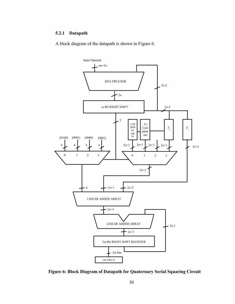
5.2.1 Datapath
A block diagram of the datapath is shown in Figure 6.
Figure 6: Block Diagram of Datapath for Quaternary Serial Squaring Circuit
2
2n+3
2n+3
2m-bits
2n-2
mn=2n
Input Operand
MULTIPLEXER
2n
2n-2
m-Bit RIGHT SHIFT
2m-Bit RIGHT SHIFT REGISTER
LINEAR ADDER ARRAY
LINEAR ADDER ARRAY
2n-1
2n+2
OUTPUT
2
2n+1 2n+1
0
2n+1
3 1
2n+2
2n+1
Left
Shift
by
one
bit
2’s
Complem
ent
T2
2n+1
T
1
2
2n+2
[0001]
2
[0100]
2
[0001]
2
[0000]
2
4 4
0
4
3 1
4
4
31
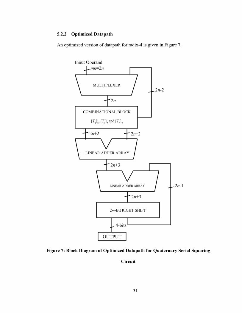
5.2.2 Optimized Datapath
An optimized version of datapath for radix-4 is given in Figure 7.
Figure 7: Block Diagram of Optimized Datapath for Quaternary Serial Squaring
Circuit
4-bits
mn=2n
Input Operand
MULTIPLEXER
LINEAR ADDER ARRAY
LINEAR ADDER ARRAY
2n-1
2n
2n+2 2n+2
2n+3
2m-Bit RIGHT SHIFT
REGISTER
2n+3
2n-2
COMBINATIONAL BLOCK
[T1]
2, [T
2]
2 and [T
3]
2
OUTPUT
32
The datapath element labeled “Combinational Logic” is implemented based on
simplifications in the formation of the intermediate terms T1, T2, and T3 and their various
sums. These simplifications exploit the choice of using β=4 as an implicit operand radix
and allow for the computation of the intermediate terms T1, T2, and T3 to be implemented
with a reduced and simplified set of RTL operations. These optimizations are described
in the next section.
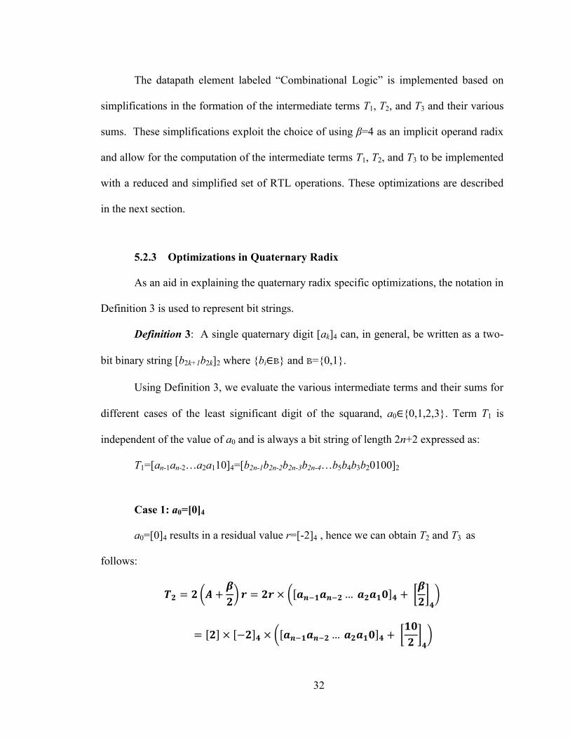
5.2.3 Optimizations in Quaternary Radix
As an aid in explaining the quaternary radix specific optimizations, the notation in
Definition 3 is used to represent bit strings.
Definition 3: A single quaternary digit [ak]4 can, in general, be written as a two-
bit binary string [b2k+1b2k]2 where {bi∈B} and B={0,1}.
Using Definition 3, we evaluate the various intermediate terms and their sums for
different cases of the least significant digit of the squarand, a0∈{0,1,2,3}. Term T1 is
independent of the value of a0 and is always a bit string of length 2n+2 expressed as:
T1=[an-1an-2…a2a110]4=[b2n-1b2n-2b2n-3b2n-4…b5b4b3b20100]2
Case 1: a0=[0]4
a0=[0]4 results in a residual value r=[-2]4 , hence we can obtain T2 and T3 as
follows:
(
) ( [
] )
( [
] )
33
( )
Combining the terms T1, T2 , T3 :
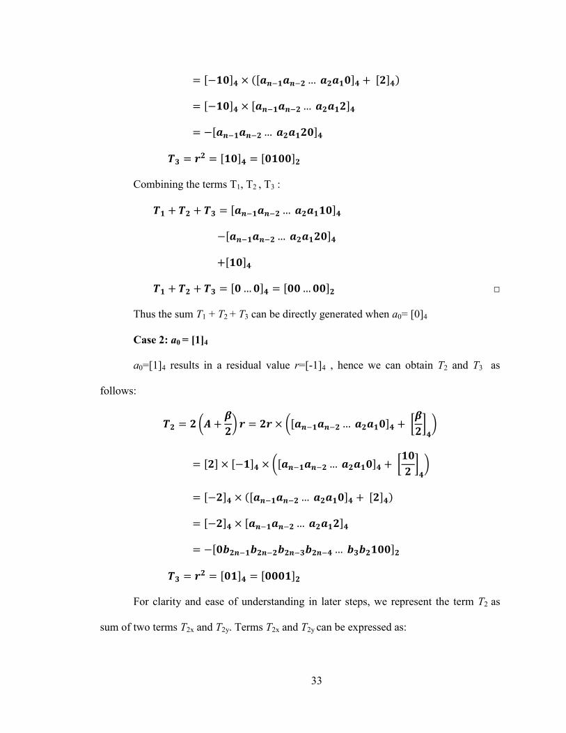
□
Thus the sum T1 + T2 + T3 can be directly generated when ɑ0= [0]4
Case 2: ɑ0 = [1]4
a0=[1]4 results in a residual value r=[-1]4 , hence we can obtain T2 and T3 as
follows:
(
) ( [
] )
( [
] )
( )
For clarity and ease of understanding in later steps, we represent the term T2 as
sum of two terms T2x and T2y. Terms T2x and T2y can be expressed as:
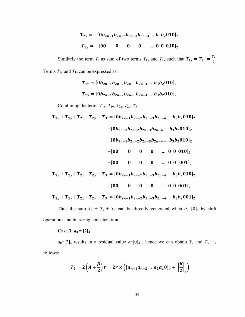
34
Similarly the term T1 as sum of two terms T1x and T1y such that
.
Terms T1x and T1y can be expressed as:
Combining the terms T1x, T1y, T2x, T2y, T3:
□
Thus the sum T1 + T2 + T3 can be directly generated when ɑ0=[0]4 by shift
operations and bit-string concatenation.
Case 3: ɑ0 = [2]4
a0=[2]4 results in a residual value r=[0]4 , hence we can obtain T2 and T3 as
follows:
(
) ( [
] )
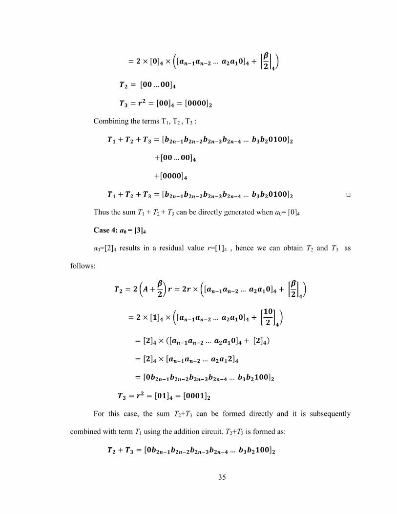
35
( [
] )
Combining the terms T1, T2 , T3 :
□
Thus the sum T1 + T2 + T3 can be directly generated when ɑ0= [0]4
Case 4: ɑ0 = [3]4
a0=[2]4 results in a residual value r=[1]4 , hence we can obtain T2 and T3 as
follows:
(
) ( [
] )
( [
] )
( )
For this case, the sum T2+T3 can be formed directly and it is subsequently
combined with term T1 using the addition circuit. T2+T3 is formed as:
36
□
T1 + T2 + T3 is obtained by performing a [2n+2]-bit addition.
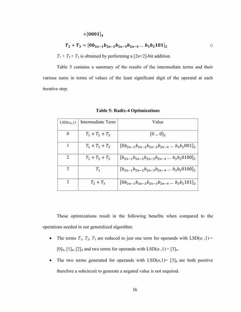
Table 5 contains a summary of the results of the intermediate terms and their
various sums in terms of values of the least significant digit of the operand at each
iterative step.
Table 5: Radix-4 Optimizations
LSD(α4,1) Intermediate Term Value
0
1
2
3
3
These optimizations result in the following benefits when compared to the
operations needed in our generalized algorithm:
The terms T1, T2, T3 are reduced to just one term for operands with LSD(α ,1) =
[0]4, [1]4, [2]4 and two terms for operands with LSD(α ,1) = [3]4.
The two terms generated for operands with LSD(α,1)= [3]4 are both positive
therefore a subcircuit to generate a negated value is not required.
37
Thus the addition operation to obtain T1+T2+T3 is required only in 25% cases.
m×2nm-bit multiplication is not required.
m-bit operand squaring is not required.
5.2.4 Combinational Logic
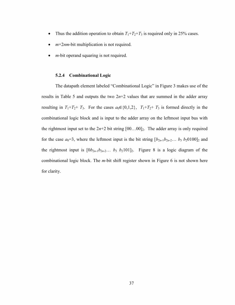
The datapath element labeled “Combinational Logic” in Figure 3 makes use of the
results in Table 5 and outputs the two 2n+2 values that are summed in the adder array
resulting in T1+T2+ T3. For the cases a0∈{0,1,2}, T1+T2+ T3 is formed directly in the
combinational logic block and is input to the adder array on the leftmost input bus with
the rightmost input set to the 2n+2 bit string [00…00]2. The adder array is only required
for the case a0=3, where the leftmost input is the bit string [b2n-1b2n-2… b3 b20100]2 and
the rightmost input is [0b2n-1b2n-2… b3 b2101]2. Figure 8 is a logic diagram of the
combinational logic block. The m-bit shift register shown in Figure 6 is not shown here
for clarity.
38
Figure 8: Circuit for the Combinational Block
2
2
1
2
2n+2
2n+2
Rightmost
adder
input
Leftmost
adder
input
3
3
0
0
2n+2
2n+2
2n+2
2n+2
ɑi
2n+2
2n+2
2n+2
2n+2
ɑi
2
1
39
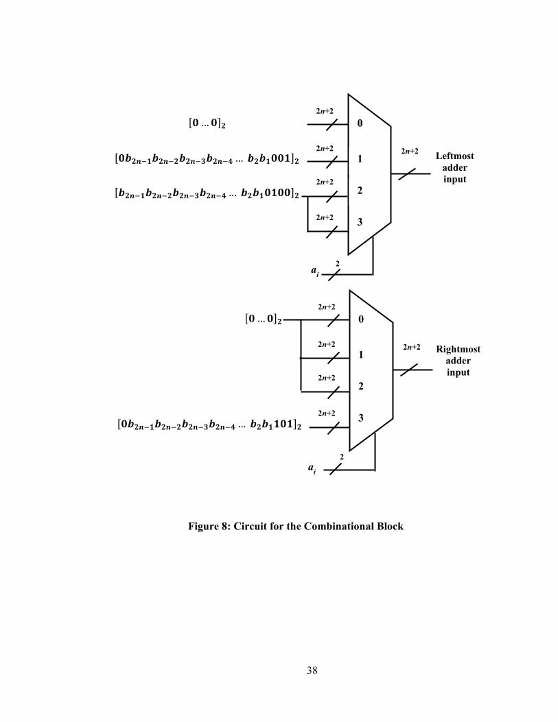
5.2.5 Controller
The circuit architecture is of the form of a clocked synchronous controller. The
state diagram for the controller is given in Figure 9 and the state table for the controller is
given in Table 6.
Controller State Diagram
Table 6: State Table for the Controller
Present State Input
inready Next State
Output
iterate
reset state 0 reset state 0
reset state 1 input state 0
input state 0 iteration state 1
iteration state 1 input state 0
The controller output depends on the present state of the controller and the input
signal ‘inready’. The output signal ‘iterate’ from the controller decides whether the
1/0
inready=0/iterate=0
s0
reset state
1/0
x
1=0/
iter
ate=
0
reset
x
1=0/it
erate
=0
s1 input state
s2
iteration state
0/1
40
datapath can accept new input squarand or compute square of a given input squarand.
The different states of controller are as follows:
Reset state:
The controller goes to reset state when an external asynchronous reset signal goes
from low to high. In reset state the controller makes output signal low. If the input signal
inready is low then the output of the controller remains low. If the inready signal is high
then controller goes from ready state to input state. The iterate signal remains low.
Input state:
The controller remains in this state as long as the inready signal is high. The
datapath can accept new squarand input in this state. When the inready signal goes low
the iterate signal goes high and the controller goes from input state to iteration state.
Iteration state:
Any input to the datapath when the controller transitions from input state to
iteration state is stored in the datapath and its square is computed in this state. The iterate
signal remains high in this state. The datapath outputs m-bits of the squared output every
clock cycle in this state. The controller goes from iteration state to input state when the
inready signal goes from low to high.
41
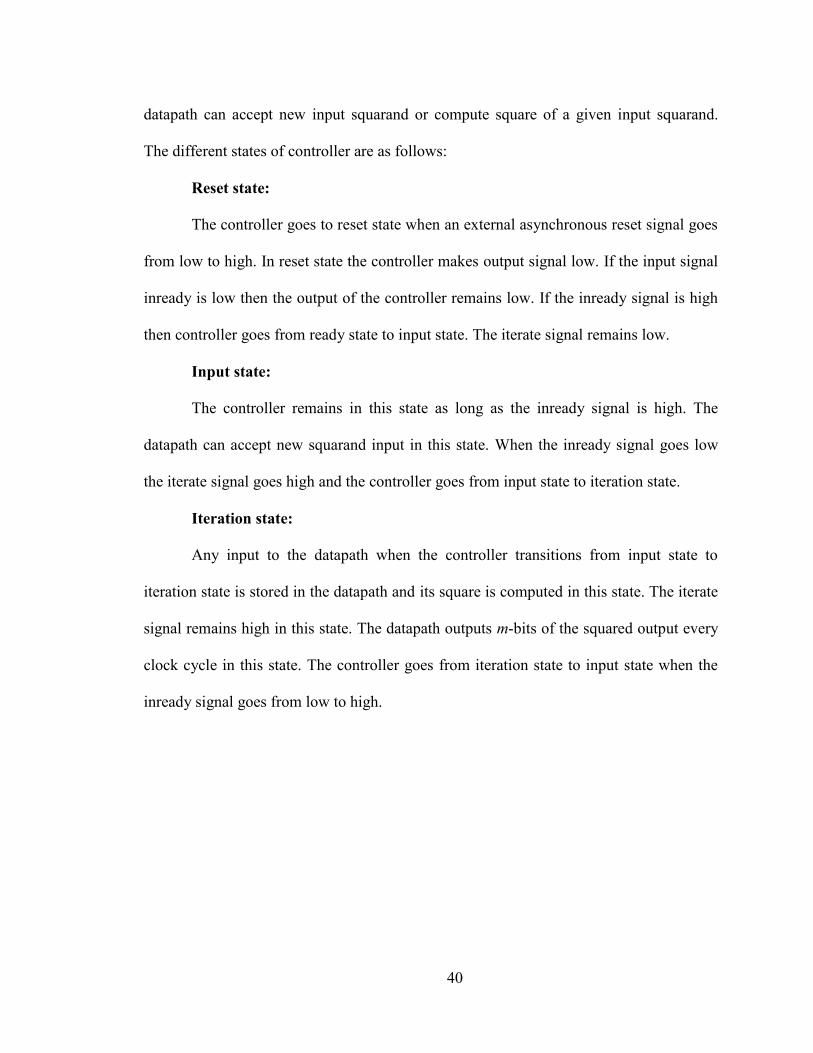
5.2.6 Combined Datapath-Controller
The combined datapath-controller circuit block diagram is given in Figure 10.
Figure 10: Block Diagram of Datapath-Controller Circuit
The circuit shown in Figure 10 has input ports for reset, inready and 2n-bit wide
squarand. The 4-bits wide output port produces 4-bits of the squared result in right-to-left
iterate
reset inready
ACCUMULATOR
LINEAR ADDER ARRAY
4-bits
mn=2n
MULTIPLEXER
Input Operand
2n-1
2n
2n+2 2n+2
2n+3
2m-Bit RIGHT SHIFT REGISTER
2n+3
2n
COMBINATIONAL BLOCK
[T1]
2, [T
2]
2 and [T
3]
2
OUTPUT
FSM

42
fashion. The implementation and evaluation of the circuit shown in Figure 10 is described
in next chapter.
43
Chapter 6
IMPLEMENTATION AND EVALUATION
Our methodology utilized the Verilog HDL to specify the algorithm at the register
transfer level. Separate modules were created for the datapath and the controller and were
instantiated in the top-level design through a third Verilog module. The Verilog
specifications were then synthesized using the Altera Quartus II design tool suite for
programmable logic and the Synopsys Design Compiler for a standard cell ASIC.
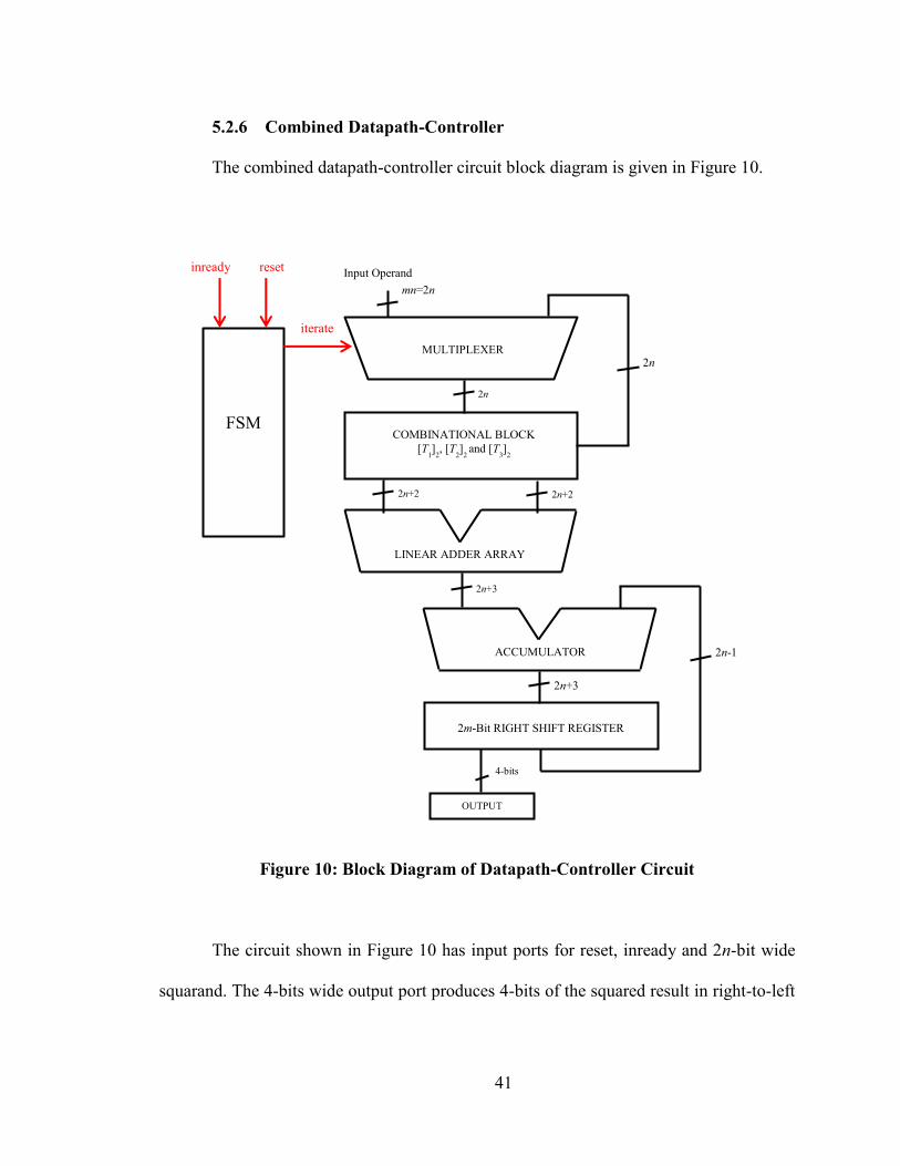
The RTL netlist obtained using Altera Quartus II for 8-bit quaternary squaring
circuit is show in Figure 11. It has the same blocks as shown in our block diagram of
datapath in Figure 7 along with the controller and registers between the multiplexer and
combinational block.
Figure 11: 8-bit Quaternary Squaring Circuit RTL Netlist
44
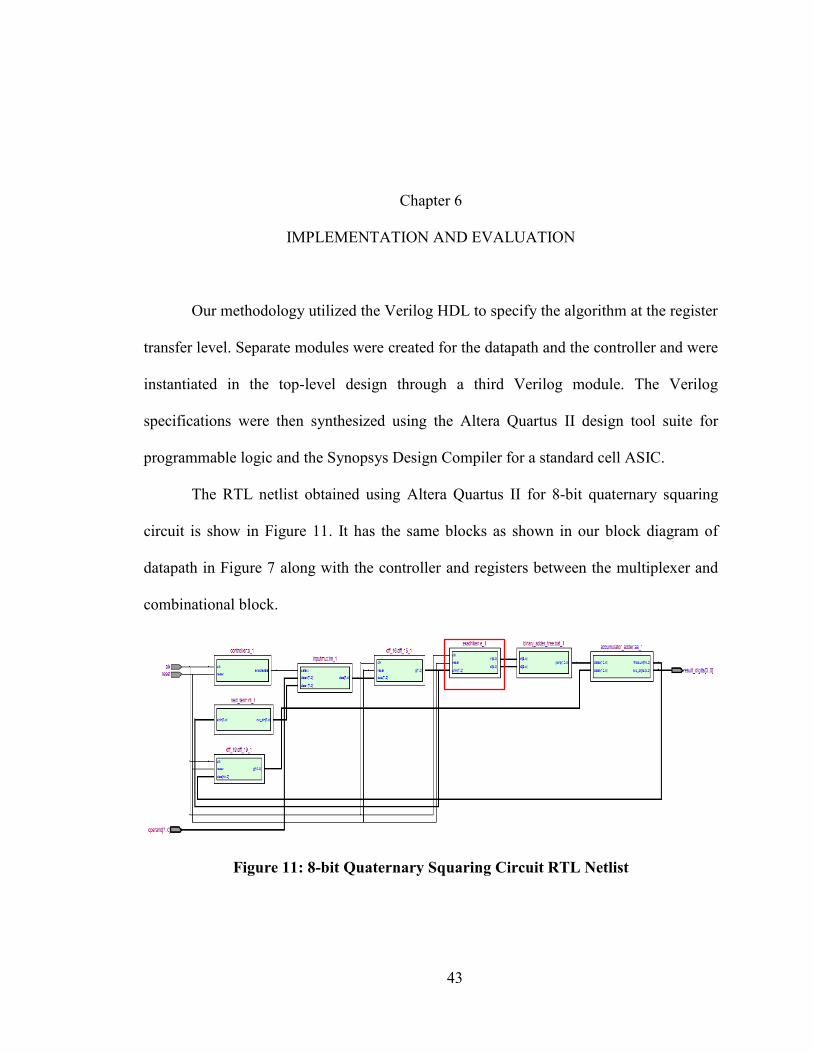
The block marked in red in Figure 11 is the combinational block which generates the
intermediate terms mentioned in Table 5. RTL netlist of this block is given in Figure 12.
Figure 12: RTL Netlist of the Combinational Block
D Q
PRE
ENA
CLR
D Q
PRE
ENA
CLR
SEL
DATAA
DATABOUT0
MUX21
SEL
DATAA
DATABOUT0
MUX21
SEL
DATAA
DATABOUT0
MUX21
SEL
DATAA
DATABOUT0
MUX21
SEL
DATAA
DATABOUT0
MUX21
SEL
DATAA
DATABOUT0
MUX21
SEL
DATAA
DATABOUT0
MUX21
SEL
DATAA
DATABOUT0
MUX21
always0~0
always0~1
always0~2
always0~3
t2[9..0]~reg0
t1~[9..0]
10' h000 --
t1~[19..10]
10' h000 --
t2~[9..0]
4' h2 --
t2~[19..10]
10' h000 --
clk
reset
shin[7..0]
t1[9..0]
t2[9..0]
t2~[29..20]
3' h0 --
1' h0 --
t2~[39..30]
3' h4 --
1' h0 --
t1~[29..20]
4' h9 --
t1~[39..30]
10' h000 --
t1[9..0]~reg0
45
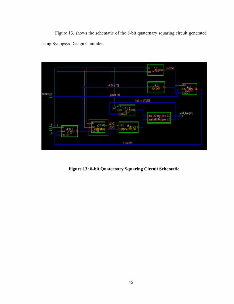
Figure 13, shows the schematic of the 8-bit quaternary squaring circuit generated
using Synopsys Design Compiler.
Figure 13: 8-bit Quaternary Squaring Circuit Schematic
46
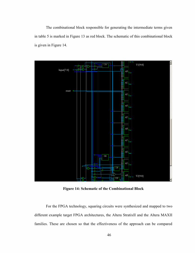
The combinational block responsible for generating the intermediate terms given
in table 5 is marked in Figure 13 as red block. The schematic of this combinational block
is given in Figure 14.
Figure 14: Schematic of the Combinational Block
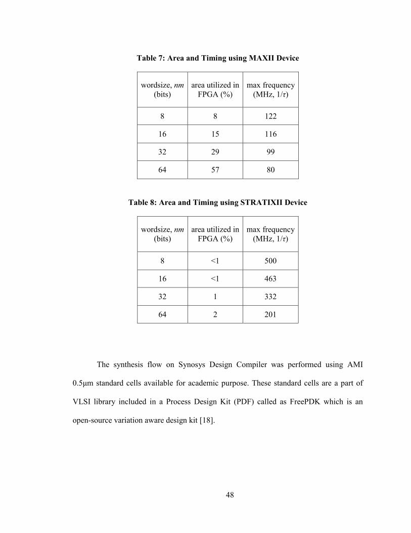
For the FPGA technology, squaring circuits were synthesized and mapped to two
different example target FPGA architectures, the Altera StratixII and the Altera MAXII
families. These are chosen so that the effectiveness of the approach can be compared
T1[9:0]
T2[9:0]
reset
Input[7:0]
47
when using a fine-grained LUT style of architecture represented by the StratixII family
and the coarser-grained PLD style of logic cells present in the MAXII family. Fine-
grained LUT architectures typically allow more flexibility in a programmable device at
the expense of increased delay due to the large number of programmable signal
interconnect subcircuits whereas coarser-grained PLD-based FPGAs such as those of the
MAXII family typically result in circuits with deceased delay characteristics but do not
have as much programmable flexibility. Tables 7 and 8 contain a summary of the
experimental results for squarand wordsizes of 8, 16, and 32 bits.
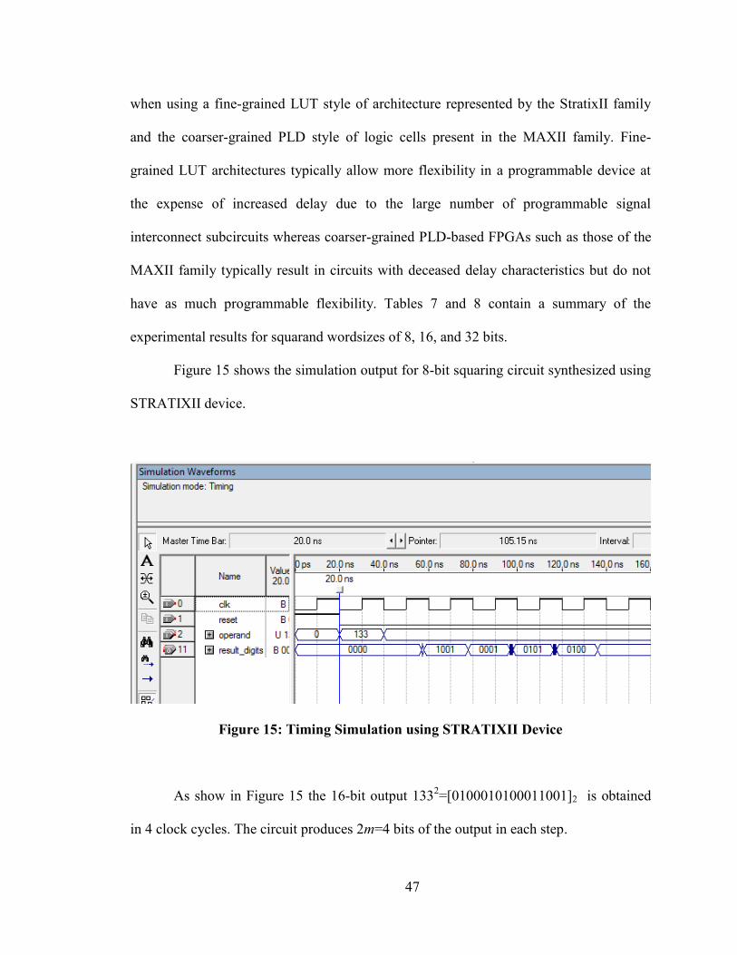
Figure 15 shows the simulation output for 8-bit squaring circuit synthesized using
STRATIXII device.
Figure 15: Timing Simulation using STRATIXII Device
As show in Figure 15 the 16-bit output 1332=[0100010100011001]2 is obtained
in 4 clock cycles. The circuit produces 2m=4 bits of the output in each step.
48
Table 7: Area and Timing using MAXII Device
wordsize, nm
(bits)
area utilized in
FPGA (%)
max frequency
(MHz, 1/τ)
8 8 122
16 15 116
32 29 99
64 57 80
Table 8: Area and Timing using STRATIXII Device
wordsize, nm
(bits)
area utilized in
FPGA (%)
max frequency
(MHz, 1/τ)
8 <1 500
16 <1 463
32 1 332
64 2 201
The synthesis flow on Synosys Design Compiler was performed using AMI
0.5μm standard cells available for academic purpose. These standard cells are a part of
VLSI library included in a Process Design Kit (PDF) called as FreePDK which is an
open-source variation aware design kit [18].
49
Table 9: Area and Timing using 0.5μm Standard Cells
wordsize, nm
(bits)
area utilized
(μm2)
max frequency
(MHz, 1/τ)
16 171504 100
32 328680 58
64 642240 31
6.1 Comparison with Other Approaches
The choice of radix β in implementation of the iterative squaring algorithm
described in this thesis allows for a trade-off in logic area versus throughput performance
in the computation of α2 when α is represented as a binary bit string. To demonstrate this
we have compared implementation of our quaternary squaring circuit with a parallel
squaring circuit and radix-4 digit-serial squaring circuit based on the method explained in
section 2.8.
The parallel squaring circuit which is based on right-to-left dual recoding is
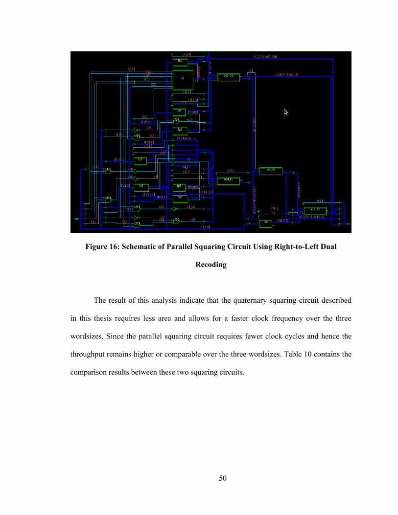
explained in section 2.7. We obtained the design files for this squaring circuit from the
researchers reporting on this method as described in [19]. The squaring circuit in [19]
was also synthesized to the standard cell library using the same design flow as that for
our quaternary squaring circuit for operand wordsizes of 16, 32, and 64 bit. The
schematic of this parallel squaring circuit obtained using Synopsys Design Compiler is
show in Figure 16.
50
Figure 16: Schematic of Parallel Squaring Circuit Using Right-to-Left Dual
Recoding
The result of this analysis indicate that the quaternary squaring circuit described
in this thesis requires less area and allows for a faster clock frequency over the three
wordsizes. Since the parallel squaring circuit requires fewer clock cycles and hence the
throughput remains higher or comparable over the three wordsizes. Table 10 contains the
comparison results between these two squaring circuits.
51
Table 10: Comparison to Right-to-Left Dual Recoded Parallel Squaring Circuit
wordsize,
nm
(bits)
area percentage
difference
frequency
percentage
difference
throughput
difference
16 -14% 75% -67%
32 -53% 93% -93%
64 -75% 84% -133%
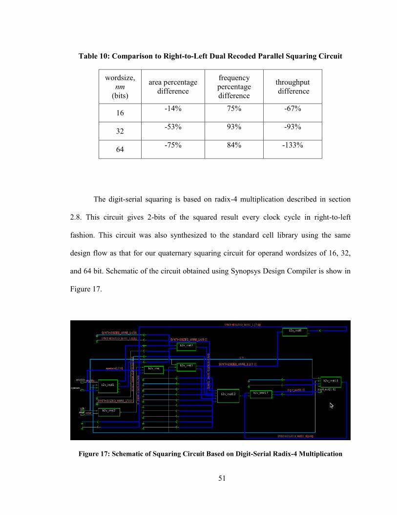
The digit-serial squaring is based on radix-4 multiplication described in section
2.8. This circuit gives 2-bits of the squared result every clock cycle in right-to-left
fashion. This circuit was also synthesized to the standard cell library using the same
design flow as that for our quaternary squaring circuit for operand wordsizes of 16, 32,
and 64 bit. Schematic of the circuit obtained using Synopsys Design Compiler is show in
Figure 17.
Figure 17: Schematic of Squaring Circuit Based on Digit-Serial Radix-4 Multiplication
52
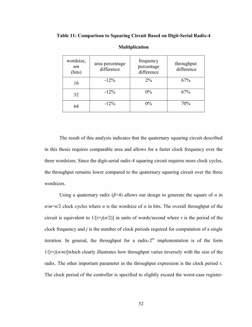
Table 11: Comparison to Squaring Circuit Based on Digit-Serial Radix-4
Multiplication
wordsize,
nm
(bits)
area percentage
difference
frequency
percentage
difference
throughput
difference
16 -12% 2% 67%
32 -12% 0% 67%
64 -12% 0% 70%
The result of this analysis indicates that the quaternary squaring circuit described
in this thesis requires comparable area and allows for a faster clock frequency over the
three wordsizes. Since the digit-serial radix-4 squaring circuit requires more clock cycles,
the throughput remains lower compared to the quaternary squaring circuit over the three
wordsizes.
Using a quaternary radix (β=4) allows our design to generate the square of α in
n/m=n/2 clock cycles where n is the wordsize of α in bits. The overall throughput of the
circuit is equivalent to 1/[τ×j(n/2)] in units of words/second where τ is the period of the
clock frequency and j is the number of clock periods required for computation of a single
iteration. In general, the throughput for a radix-2m implementation is of the form
1/[τ×j(n/m)]which clearly illustrates how throughput varies inversely with the size of the
radix. The other important parameter in the throughput expression is the clock period τ.
The clock period of the controller is specified to slightly exceed the worst-case register-
53
to-register path delay through the datapath portion of the circuit. The efficiency of the
design and implementation is the controlling factor for τ.
The datapath in our design can be further optimized through increasing the use of
pipelining principles allowing for further increasing the clock frequency value. More
pipelining would result in breaking the datapath into smaller combinational subcircuits
that are encapsulated by internal registers thereby decreasing the worst-case register-to-
register delay and allowing for an increased clock frequency. Such a pipelined approach
would have most certainly increased the overall throughput; however, for the sake of
clarity and explanation of the algorithm, our example contains minimal pipelining. The
throughput of the pipelined version is 1/[τp×P(n/2)] where P>j is the total number of
pipeline stages and τp is the period of the clock signal for the optimized pipelined version
(τp<τ).
Another optimization is to reuse internal datapath registers. It may have been
possible to decrease the number of internal registers by reusing them to contain
intermediate results. Register T2 is reused in our example to contain intermediate results
in the computation of term T2; however, other register re-usage opportunities could have
also been exploited. We chose not to implement this optimization technique in the
example circuit, for the sake of improving clarity and understanding.
54
Chapter 7
CONCLUSION AND FUTURE RESEARCH
A digit-serial squaring algorithm based on squarands expressed in any arbitrary
radix number system is formulated and implemented in a prototype FPGA logic circuit.
The algorithm is motivated by a Vedic technique and was generalized for arbitrary radix
values and to account for all possible cases of the value of the squarand. Further
motivation for the development of this technique is to allow arithmetic logic circuit
designers the ability to trade-off resulting circuit logic resources with throughput by
varying the number of bits produced in each iteration by an appropriate choice of the
working radix value.
The results of the prototype implementation are analyzed and found to offer a
desirable alternative as compared to past squaring circuit approaches where either a bit-
serial or fully parallel type of circuit is used. The method is applicable for
implementation in software or in hardware. Hardware implementations can be realized in
a variety of target technologies including programmable devices, standard cell library
ASICs, full-custom ASICs, or any combination of these.
In the current implementation of quaternary squaring circuit using the digit-serial
squaring algorithm the binary adder array is required to compute the sum of T1 and T2+T3
when ɑ0 = [3]4, while the sum T1+T2+T3 is generated directly through shift and
concatenation operations when ɑ0 ∈{0,1,2}. We believe that by an appropriate choice
55
of radix-4 digit set simplifications can be obtained in the case where ɑ0 = [3]4,
allowing for computation of the sum T1+T2+T3 to be implemented with further reduced
and simplified set of RTL operations and possibly removing the need of any binary adder
array. This can result into further reduction of area and latency of the quaternary squaring
circuit.
Future work also includes the development of other arithmetic circuits using the
squaring computation as an atomic operation such as the design of multiplication and
division architectures. We also plan to implement approximate squaring circuits by
modifying the method described here to begin computation of the square by truncating or
rounding the squarand at the desired intermediate digit position resulting in increased
throughput at the expense of generation of an approximate result. The approximate
squaring circuit will also be investigated for use as a basic atomic operation in other
arithmetic circuits.
We also intend to formulate an asynchronous version of the prototype circuit
using the recently developed NCL synthesis tool UNCLE [17]. We anticipate the
asynchronous version of the squaring circuit to demonstrate increased throughput and
lower power dissipation as compared to the clocked synchronous implementation
described here.
56
REFERENCES
[1] Pihl, J. and Aas, E.J., “A multiplier and squarer generator for high performance
DSP applications,” IEEE 39th
Midwest Symposium on Circuits and System, vol. 1,
pp. 109-112, Aug 1996.
[2] Stallings, W., Cryptography and Network Security: Principles and Practices.
Prentice-Hall, 4th
ed., Upper Saddle River, NJ: 2006.
[3] Chen, T.C., “A Binary Multiplication Based on Squaring” IEEE Trans. Computer,
vol. C-20, no. 6, pp. 678-680, June 1971.
[4] Pekmestzi, K.Z., Kalivas, P., and Moshopoulos, N., “Long unsigned number
systolic serial multipliers and squarers,” IEEE Transactions on Circuits and
Systems II: Analog and Digital Signal Processing, vol. 48, no. 3, pp. 316-321,
Mar 2001.
[5] Dadda, L., “Squares for Binary Numbers in Serial Form” in proc. IEEE
Symposium on Computer Arithmetic, pp. 173-180, June 1985.
[6] Chaniotakis, E., Kalivas, P., and Pekmestzi, K.Z., “Long number bit-serial
squarers,” in proc. IEEE Symposium on Computer Arithmetic, pp. 29-36, June
2005.
[7] Ienne, P., and Viredaz, M.A., “Bit-serial multipliers and squarers,” IEEE
Transactions on Computers, vol. 43, no. 12, pp. 1445-1450, December 1994.
[8] Yoo, J.T., Kent, K.F., Smith, F., and Gopalakrishnan, G.G., “A fast parallel
squarer based on divide and-conquer,” IEEE J. Solid-State Circuits, vol. 32, no.
6, pp. 909-912., June 1997.
[9] Strollo, A.G.H. and DeCaro, D., “Booth Folding Encoding for High Performance
Squarer Circuits,” IEEE Trans. Circuits and System-I1 Analog and Digital Signal
Processing, vol. 50, no. 5, pp. 250-254, May 2003.
[10] Fengqi, Y.Y. and Willson, A.N., “Multirate digital squarer architectures,” in proc.
IEEE Int. Conf. on Electronics, Circuits and Systems, vol. 1, pp. 177-180, Sept.
2001.
[11] DeCaro, D. and Strollo, A.G.M., “Parallel squarer using Booth-folding
technique,” Electron, Lett., vol. 37, no. 6, pp. 346-347, Mar. 2001.
57
[12] Matula, D.W., “Higher Radix Squaring Operations Employing Left-to-Right Dual
Recoding,” in proc. IEEE Symposium on Computer Arithmetic, pp. 39-47, June
2009.
[13] Datla, S.R., Thornton, M.A., and Matula, D.W., “A Low Power High
Performance Radix-4 Approximate Squaring Circuit,” in proc. IEEE International
Conference on Application-specific Systems, Architectures and Processors, pp.
91-97, July 2009.
[14] Pihl, J. and Aas, E.J., “A multiplier and squarer generator for high performance
DSP applications,” in proc. IEEE 39th
Midwest symposium on Circuits and
System, pp. 109-112, Aug. 1996.
[15] Kornerup, P. and Matula, D.W., Finite Precision Number Systems and
Arithmetic, Cambridge University Press, Cambridge, United Kingdom, ISBN
978-0-521-76135-2, 2010.
[16] Miller, D.M. and Thornton, M.A., Multiple-Valued Logic Concepts and
Representations, Morgan & Claypool Publishers, San Rafael, California, ISBN
10-1598291904, 2008.
[17] Reese, R.B., Smith, S.A., and Thornton, M.A., Uncle – an RTL Approach to
Asynchronous Design, in proc. IEEE International Symposium on Asynchronous
Circuits and Systems (ASYNC), May 7-9, 2012.
[18] Stine, J., et al., FreePDK: An Open-source Variation-aware Design Kit, in proc.
IEEE International Conference on Microelectronic Systems Education (MSE), pp.
173-174, June 2-4, 2007.
[19] J. Moore, D.W. Matula, M.A. Thornton “A Low Power Radix-4 Dual Recoded
Integer Squaring Implementation For Use in Design of Application Specific
Arithmetic Circuits”, Asilomar Conference on Signals, Systems and Computers,
October 2008.
[20] M. Ercegovac “Left-to-Right Squarer with Overlapped LS and MS parts”,
Conference Record of the 37th Asilomar Conference on Signal Systems and
Computers, vol. 2, pp.1451-1455, November 2003.
[21] H. Ling, “High-speed computer multiplication using a multiple-bit decoding
algorithm,” IEEE Trans. Computers, C-19, pp. 706-709, August 1970.
[22] Andrew D. Booth, “A Signed Binary Multiplication Technique”, The Quarterly
Journal of Mechanics and Applied Mathematics, vol. 4, pp. 2, August 1950.