A Comparative Study of Symmetrical Cockcroft-Walton ...
11
Research Article A Comparative Study of Symmetrical Cockcroft-Walton Voltage Multipliers Mohsen Ruzbehani Laser & Optics Research School, NSTRI, Tehran 14399-51113, Iran Correspondence should be addressed to Mohsen Ruzbehani; [email protected] Received 18 July 2016; Accepted 18 December 2016; Published 16 January 2017 Academic Editor: George S. Tombras Copyright © 2017 Mohsen Ruzbehani. is is an open access article distributed under the Creative Commons Attribution License, which permits unrestricted use, distribution, and reproduction in any medium, provided the original work is properly cited. Decades aſter invention of the Cockcroſt-Walton voltage multiplier, it is still being used in broad range of high voltage and ac to dc applications. High voltage ratio, low voltage stress on components, compactness, and high efficiency are its main features. Due to the problems of original circuit, reduction of output ripple and increase of accessible voltage level were the motivations for scientist to propose new topologies. In this article a comparative study on these voltage multipliers was presented. By simulations and experimental prototypes, characteristics of the topologies have been compared. In addition to the performances, components count, voltage stress on the components, and the difficulty and cost of construction are other factors which have been considered in this comparison. An easy to use table which summarized the characteristics of VMs was developed, which can be used as a decision mean for selecting of a topology based on the requirements. It is shown that, due to the application, sometimes a simple and not very famous topology is more effective than a famous one. 1. Introduction High voltage dc power supplies are widely used for many applications, such as particle accelerators, X-ray systems, electron microscopes, photon multipliers, electrostatic sys- tems, lasers systems, and electrostatic coating [1–5]. ere are several approaches in producing high voltage dc sources depending on the desired voltage and current levels. A more usual choice when a power supply with high voltage and low current is needed is the Cockcroſt-Walton voltage multiplier (CWVM). High voltage ratio, low voltage stress on the diodes and capacitors, compactness, and high efficiency are the main reasons for this choice [3, 5, 6]. Furthermore it can be used in medium voltage applications when the current is low and simple circuit is the matter, like portable pulsed power applications and handheld devices [7–9]. e CWVM has the unique characteristic of imposing equal voltage stresses on every stage. Its construction is also simple and easy to implement [10]. Usually, in modern types of voltage multipliers there are three stages; a high frequency inverter which produces fast dynamic voltage source with controllable duty cycle to control the current and voltage level, a transformer, and a CW voltage multiplier [11]. In this article only the topologies of VMs, regardless of inverter construction, are studied. Historically the original idea was proposed by Greinacher in 1921. However, it did not get attention for a long time until Cockcroſt and Walton performed their experiment using this circuit in 1932 [12]. Large output voltage ripple and output voltage drop were the main problems of the original half-wave voltage multiplier. Consequently, to overcome these prob- lems, a symmetrical voltage multiplier (SVM) was developed by Heilpern in 1954 by adding an extra oscillating column of capacitors and a stack of rectifiers [1, 13] Because voltage ripple in a half-wave rectifier due to the charge and discharge of capacitors has almost a triangular-like shape, by using two voltage sources with 180 ∘ phase difference, the overall voltage ripple magnitude can be reduced greatly. If the ripple was an isosceles triangle shaped waveform, the opposite phase could exactly cancel out the voltage peaks so that the voltage ripple would be disappeared in the output voltage. However, this is not the case, so the ripple will not be removed completely, and the result is only reduction of ripple amplitude. is is the main feature of a symmetrical voltage multiplier. Based on Hindawi Journal of Electrical and Computer Engineering Volume 2017, Article ID 4805268, 10 pages https://doi.org/10.1155/2017/4805268
Transcript of A Comparative Study of Symmetrical Cockcroft-Walton ...
Research ArticleA Comparative Study of Symmetrical Cockcroft-WaltonVoltage Multipliers
Mohsen Ruzbehani
Laser & Optics Research School, NSTRI, Tehran 14399-51113, Iran
Correspondence should be addressed to Mohsen Ruzbehani; [email protected]
Received 18 July 2016; Accepted 18 December 2016; Published 16 January 2017
Academic Editor: George S. Tombras
Copyright © 2017 Mohsen Ruzbehani. This is an open access article distributed under the Creative Commons Attribution License,which permits unrestricted use, distribution, and reproduction in any medium, provided the original work is properly cited.
Decades after invention of the Cockcroft-Walton voltage multiplier, it is still being used in broad range of high voltage and acto dc applications. High voltage ratio, low voltage stress on components, compactness, and high efficiency are its main features.Due to the problems of original circuit, reduction of output ripple and increase of accessible voltage level were the motivations forscientist to propose new topologies. In this article a comparative study on these voltage multipliers was presented. By simulationsand experimental prototypes, characteristics of the topologies have been compared. In addition to the performances, componentscount, voltage stress on the components, and the difficulty and cost of construction are other factors which have been considered inthis comparison. An easy to use table which summarized the characteristics of VMs was developed, which can be used as a decisionmean for selecting of a topology based on the requirements. It is shown that, due to the application, sometimes a simple and notvery famous topology is more effective than a famous one.
1. Introduction
High voltage dc power supplies are widely used for manyapplications, such as particle accelerators, X-ray systems,electron microscopes, photon multipliers, electrostatic sys-tems, lasers systems, and electrostatic coating [1–5]. Thereare several approaches in producing high voltage dc sourcesdepending on the desired voltage and current levels. Amore usual choice when a power supply with high voltageand low current is needed is the Cockcroft-Walton voltagemultiplier (CWVM). High voltage ratio, low voltage stress onthe diodes and capacitors, compactness, and high efficiencyare the main reasons for this choice [3, 5, 6]. Furthermoreit can be used in medium voltage applications when thecurrent is low and simple circuit is the matter, like portablepulsed power applications and handheld devices [7–9]. TheCWVM has the unique characteristic of imposing equalvoltage stresses on every stage. Its construction is also simpleand easy to implement [10]. Usually, in modern types ofvoltage multipliers there are three stages; a high frequencyinverter which produces fast dynamic voltage source withcontrollable duty cycle to control the current and voltage
level, a transformer, and a CW voltage multiplier [11]. Inthis article only the topologies of VMs, regardless of inverterconstruction, are studied.
Historically the original idea was proposed byGreinacherin 1921. However, it did not get attention for a long time untilCockcroft andWalton performed their experiment using thiscircuit in 1932 [12]. Large output voltage ripple and outputvoltage dropwere themain problems of the original half-wavevoltage multiplier. Consequently, to overcome these prob-lems, a symmetrical voltage multiplier (SVM) was developedby Heilpern in 1954 by adding an extra oscillating columnof capacitors and a stack of rectifiers [1, 13] Because voltageripple in a half-wave rectifier due to the charge and dischargeof capacitors has almost a triangular-like shape, by using twovoltage sources with 180∘ phase difference, the overall voltageripple magnitude can be reduced greatly. If the ripple was anisosceles triangle shaped waveform, the opposite phase couldexactly cancel out the voltage peaks so that the voltage ripplewould be disappeared in the output voltage. However, this isnot the case, so the ripple will not be removed completely, andthe result is only reduction of ripple amplitude. This is themain feature of a symmetrical voltage multiplier. Based on
HindawiJournal of Electrical and Computer EngineeringVolume 2017, Article ID 4805268, 10 pageshttps://doi.org/10.1155/2017/4805268
2 Journal of Electrical and Computer Engineering
Vs
C1
C2
C3
C4
C5
C6
C7
C8
D1 D2 D3 D4 D5 D6 D7 D8
Rl
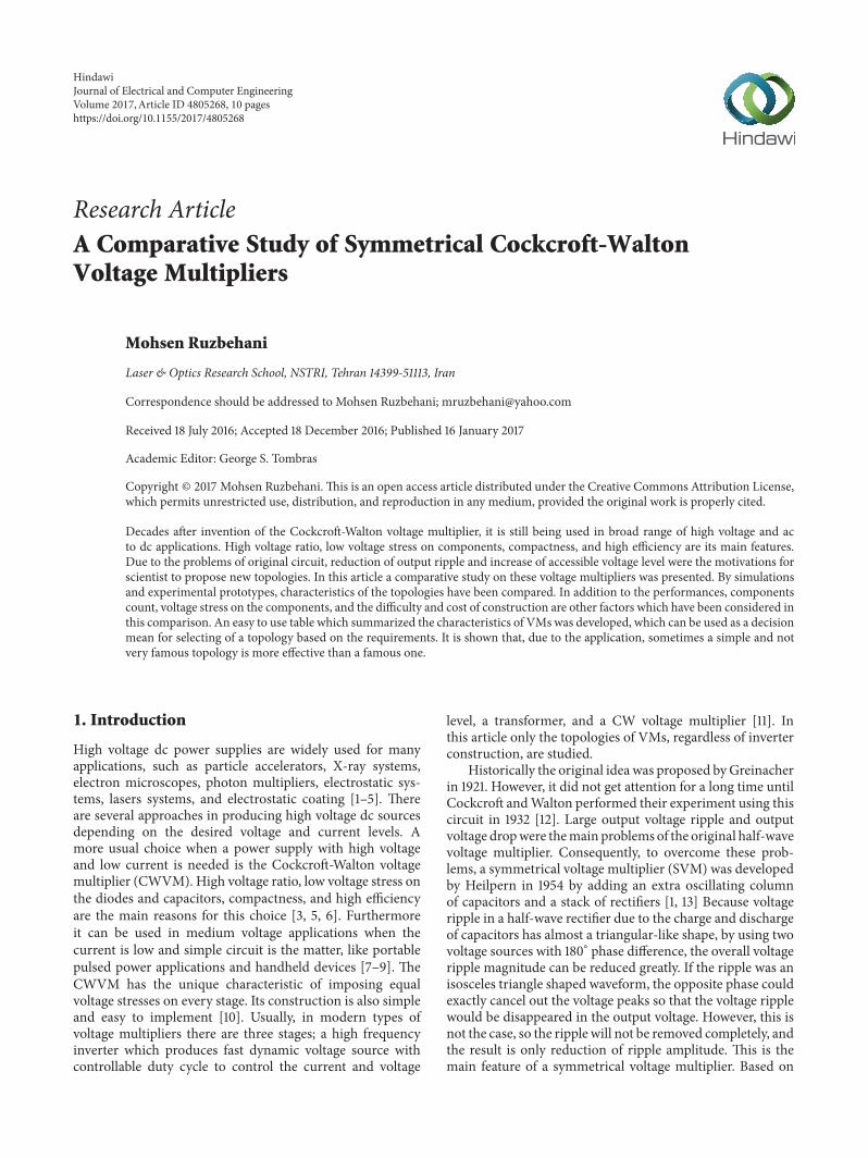
Figure 1: Schematic circuit of a basic 4-stage Cockcroft-Waltonvoltage multiplier.
this idea, recently a three-phase symmetrical voltage multi-plier with six oscillating columns and one smootheningcolumn has been proposed [2, 14]. Furthermore, there areother topologies which based on this idea have lower voltageripple compared to the conventional one, which will bestudied in this article. Other types of voltagemultipliers basedon CWVM have been developed recently which a CWVM isfed by a matrix converter [6]. The matrix converter generatesan adjustable frequency and adjustable-amplitude current,which is injected into the CWVM to regulate the dc outputvoltage and smooth its ripple. However, in this article, theCWVM is the subject, regardless of how it may be fed.
The comparison of these VMs is important becauseselecting a topology for an application due to many factorsinvolved is not a straightforward task. The range of outputvoltage level, necessary safety factors, ground-returned orbipolar output, and speed of response and so on are the mainfactors which should be considered in such selection. To thebest of author’s knowledge, until now such comparison hasnot been made.
This paper is organized as follows. The mathematicalmodel of the CWVM is reviewed in Section 2. Symmetricalvoltage multipliers are introduced in Section 3. Comparisonsbetween the symmetrical VMs by simulation are presented inSection 4. In Section 5 experimental low voltage prototypesare constructed to justify the results of simulations. Finallyconclusion is given in Section 6.
2. Basic Voltage Multiplier
Figure 1 shows a basic 4-stage Cockcroft-Walton voltage mul-tiplier circuit. It consists of two capacitor columns, namely,oscillating and smoothening columns. Oscillating columncapacitors (𝐶1, 𝐶3, 𝐶5, and 𝐶7) are charged in half cycleby upward odd numbered diodes (𝐷1, 𝐷3, 𝐷5, and 𝐷7,respectively) and in next half cycle the smoothening columncapacitors (𝐶2,𝐶4,𝐶6, and𝐶8) are charged by downward evennumbered didoes (𝐷2, 𝐷4, 𝐷6, and 𝐷8). In steady state, inno-load condition, every capacitor in smoothening column ischarged to 2𝑉max, that is, two times ofmaximum input voltagemagnitude. Therefore, the maximum value of output voltageis 2𝑛𝑉max in which 𝑛 is the number of multiplier stages (here𝑛 = 4).
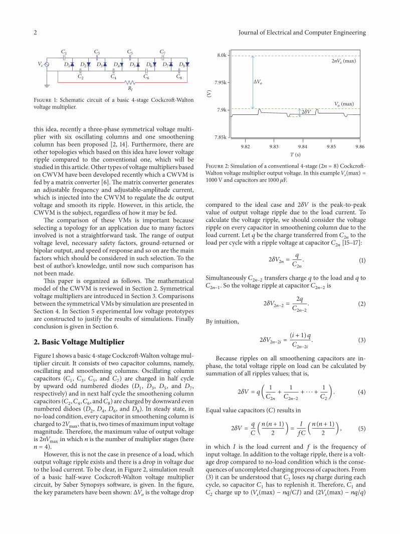
However, this is not the case in presence of a load, whichoutput voltage ripple exists and there is a drop in voltage dueto the load current. To be clear, in Figure 2, simulation resultof a basic half-wave Cockcroft-Walton voltage multipliercircuit, by Saber Synopsys software, is given. In the figure,the key parameters have been shown: Δ𝑉𝑜 is the voltage drop
8.0k
7.95k
7.9k
7.85k
(V)
ΔVo
2𝛿V
Vo (max)
2nVs (max)
9.82 9.83 9.84 9.85 9.86
T (s)
Figure 2: Simulation of a conventional 4-stage (2𝑛 = 8) Cockcroft-Walton voltage multiplier output voltage. In this example𝑉𝑠(max) =1000V and capacitors are 1000 𝜇F.
compared to the ideal case and 2𝛿𝑉 is the peak-to-peakvalue of output voltage ripple due to the load current. Tocalculate the voltage ripple, we should consider the voltageripple on every capacitor in smoothening column due to theload current. Let 𝑞 be the charge transferred from 𝐶2𝑛 to theload per cycle with a ripple voltage at capacitor 𝐶2𝑛 [15–17]:
2𝛿𝑉2𝑛 = 𝑞𝐶2𝑛 . (1)
Simultaneously 𝐶2𝑛−2 transfers charge 𝑞 to the load and 𝑞 to𝐶2𝑛−1. So the voltage ripple at capacitor 𝐶2𝑛−2 is2𝛿𝑉2𝑛−2 = 2𝑞𝐶2𝑛−2 . (2)
By intuition,
2𝛿𝑉2𝑛−2𝑖 = (𝑖 + 1) 𝑞𝐶2𝑛−2𝑖 . (3)
Because ripples on all smoothening capacitors are in-phase, the total voltage ripple on load can be calculated bysummation of all ripples values; that is,
2𝛿𝑉 = 𝑞( 1𝐶2𝑛 +1𝐶2𝑛−2 + ⋅ ⋅ ⋅ +
1𝐶2) . (4)
Equal value capacitors (𝐶) results in2𝛿𝑉 = 𝑞𝐶 (𝑛 (𝑛 + 1)2 ) = 𝐼𝑓𝐶 (𝑛 (𝑛 + 1)2 ) , (5)
in which 𝐼 is the load current and 𝑓 is the frequency ofinput voltage. In addition to the voltage ripple, there is a volt-age drop compared to no-load condition which is the conse-quences of uncompleted charging process of capacitors. From(3) it can be understood that 𝐶2 loses 𝑛𝑞 charge during eachcycle, so capacitor 𝐶1 has to replenish it. Therefore, 𝐶1 and𝐶2 charge up to (𝑉𝑠(max) − 𝑛𝑞/𝐶𝐽) and (2𝑉𝑠(max) − 𝑛𝑞/𝑞)
Journal of Electrical and Computer Engineering 3
instead of 𝑉𝑠(max) and 2𝑉𝑠(max), respectively. In the samemanner the voltage drop in all smoothening capacitors couldbe calculated. In general we will have [15]
Δ𝑉2 = 𝑞𝐶𝑛,Δ𝑉4 = 𝑞𝐶 [2𝑛 + (𝑛 − 1)] ,
...Δ𝑉2𝑛 = 𝑞𝐶 [2𝑛 + 2 (𝑛 − 1) + ⋅ ⋅ ⋅ + 2 × 2 + 1] .
(6)
Adding all 𝑛 voltage drops gives the total voltage drop on load:Δ𝑉total = 𝑞𝐶 (23𝑛3 + 12𝑛2 − 𝑛6)= 𝐼𝑓𝐶 (23𝑛3 + 12𝑛2 − 𝑛6) .
(7)
Recently with more detailed analysis it has been shownthat the above formula needs a small correction [18].Howeverthe difference is of secondary importance for practical use,because it does not concern the leading order in 𝑛. From(7) and (5) it is clear for a given value of 𝑛, by increasingload current, voltage drop and voltage ripple increase pro-portionally. To compensate this effect the value of 𝑓 × 𝐶should be increased. Usually increasing frequency has lowercost compared to increasing the capacitors values. Moreoverfrom these relations it is also clear that increasing number ofstages will increase these drop voltage and ripple amplitude.Therefore, there is an optimum value for n which gives themaximum accessible output voltage when other parametersare fixed. This optimum value is as follows [13]:
𝑛opt = √𝑉𝑠 (max) 𝑓𝐶𝐼 . (8)
Hence, the maximum accessible voltage is as follows.
𝑉𝑜 (max) = 2𝑛opt𝑉𝑠 (max)− 𝐼𝑓𝐶 (23𝑛3opt + 12𝑛2opt −
𝑛opt6 ) .(9)
To exceed the restriction of (9) and also to decreasethe output voltage ripple value, several configurations havebeen proposed which are the subject of next section. It isworth mentioning that a proper selection of nonequal valuecapacitors (𝐶2𝑖 = 𝐶2𝑖−1 = (𝑛 + 1 − 𝑖)𝐶) will result in betterresponse compared to the classical case (𝐶2𝑖 = 𝐶2𝑖−1 = 𝐶)[19].The result can be extended to the symmetrical cases withminor modifications.
3. Symmetrical Versions of Voltage Multiplier
3.1. Conventional Symmetrical Voltage Multiplier. As men-tioned in previous section, by increasing number of stages,
Vs1
Vs2
C1 C2 C3 C4
C1x C3xC2x C4x
C1y C3yC2y C4y
Rl
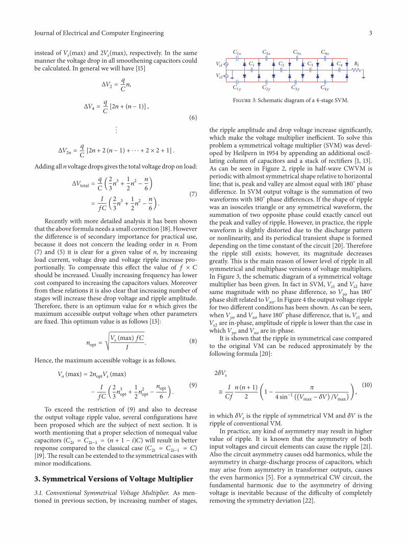
Figure 3: Schematic diagram of a 4-stage SVM.
the ripple amplitude and drop voltage increase significantly,which make the voltage multiplier inefficient. To solve thisproblem a symmetrical voltage multiplier (SVM) was devel-oped by Heilpern in 1954 by appending an additional oscil-lating column of capacitors and a stack of rectifiers [1, 13].As can be seen in Figure 2, ripple in half-wave CWVM isperiodic with almost symmetrical shape relative to horizontalline; that is, peak and valley are almost equal with 180∘ phasedifference. In SVM output voltage is the summation of twowaveforms with 180∘ phase differences. If the shape of ripplewas an isosceles triangle or any symmetrical waveform, thesummation of two opposite phase could exactly cancel outthe peak and valley of ripple. However, in practice, the ripplewaveform is slightly distorted due to the discharge patternor nonlinearity, and its periodical transient shape is formeddepending on the time constant of the circuit [20]. Thereforethe ripple still exists; however, its magnitude decreasesgreatly. This is the main reason of lower level of ripple in allsymmetrical and multiphase versions of voltage multipliers.In Figure 3, the schematic diagram of a symmetrical voltagemultiplier has been given. In fact in SVM, 𝑉𝑠1 and 𝑉𝑠2 havesame magnitude with no phase difference, so 𝑉𝑦𝑜 has 180∘phase shift related to𝑉𝑥𝑜. In Figure 4 the output voltage ripplefor two different conditions has been shown. As can be seen,when 𝑉𝑦𝑜 and 𝑉𝑥𝑜 have 180∘ phase difference, that is, 𝑉𝑠1 and𝑉𝑠2 are in-phase, amplitude of ripple is lower than the case inwhich 𝑉𝑦𝑜 and 𝑉𝑥𝑜 are in-phase.
It is shown that the ripple in symmetrical case comparedto the original VM can be reduced approximately by thefollowing formula [20]:
2𝛿𝑉𝑠≅ 𝐼𝐶𝑓 𝑛 (𝑛 + 1)2 (1 − 𝜋4 sin−1 ((𝑉max − 𝛿𝑉) /𝑉max)) ,
(10)
in which 𝛿𝑉𝑠 is the ripple of symmetrical VM and 𝛿𝑉 is theripple of conventional VM.
In practice, any kind of asymmetry may result in highervalue of ripple. It is known that the asymmetry of bothinput voltages and circuit elements can cause the ripple [21].Also the circuit asymmetry causes odd harmonics, while theasymmetry in charge-discharge process of capacitors, whichmay arise from asymmetry in transformer outputs, causesthe even harmonics [5]. For a symmetrical CW circuit, thefundamental harmonic due to the asymmetry of drivingvoltage is inevitable because of the difficulty of completelyremoving the symmetry deviation [22].
4 Journal of Electrical and Computer Engineering
9.9 9.92 9.94 9.96 9.98T (s)
7.5k
7.6k
7.7k
7.8k
7.9k
(V)
10.0
Vxo and Vyo have 180∘ phase difference
Vxo and Vyo are in-phase
Figure 4: Output voltage ripple of a symmetrical voltage multiplierfor two cases of in-phase and 180∘ out of phase power sources.
Vs
C1 C2 C3 C4
C1x C3xC2x
C1y C3yC2y
Rl
Figure 5: Schematic diagram of a 4-stage HSVM.
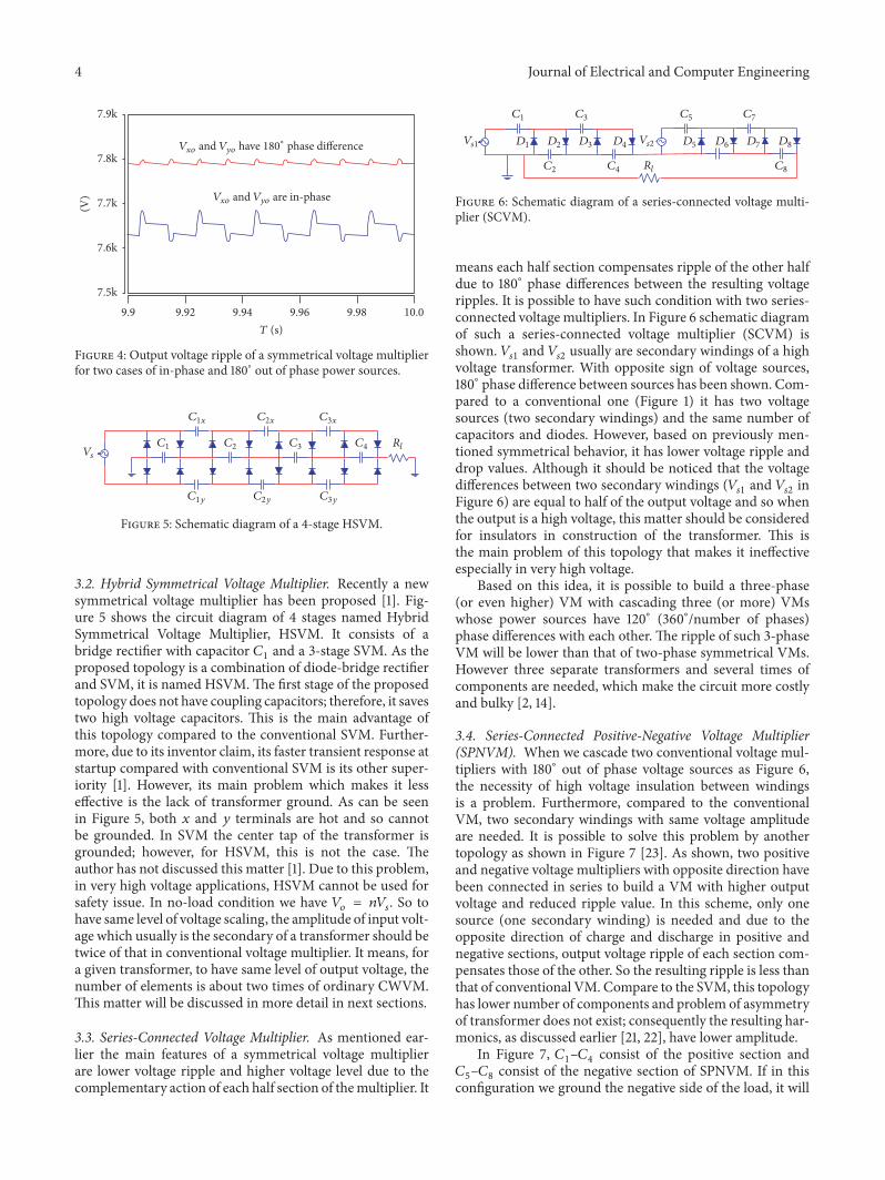
3.2. Hybrid Symmetrical Voltage Multiplier. Recently a newsymmetrical voltage multiplier has been proposed [1]. Fig-ure 5 shows the circuit diagram of 4 stages named HybridSymmetrical Voltage Multiplier, HSVM. It consists of abridge rectifier with capacitor 𝐶1 and a 3-stage SVM. As theproposed topology is a combination of diode-bridge rectifierand SVM, it is named HSVM.The first stage of the proposedtopology does not have coupling capacitors; therefore, it savestwo high voltage capacitors. This is the main advantage ofthis topology compared to the conventional SVM. Further-more, due to its inventor claim, its faster transient response atstartup compared with conventional SVM is its other super-iority [1]. However, its main problem which makes it lesseffective is the lack of transformer ground. As can be seenin Figure 5, both 𝑥 and 𝑦 terminals are hot and so cannotbe grounded. In SVM the center tap of the transformer isgrounded; however, for HSVM, this is not the case. Theauthor has not discussed this matter [1]. Due to this problem,in very high voltage applications, HSVM cannot be used forsafety issue. In no-load condition we have 𝑉𝑜 = 𝑛𝑉𝑠. So tohave same level of voltage scaling, the amplitude of input volt-age which usually is the secondary of a transformer should betwice of that in conventional voltage multiplier. It means, fora given transformer, to have same level of output voltage, thenumber of elements is about two times of ordinary CWVM.This matter will be discussed in more detail in next sections.
3.3. Series-Connected Voltage Multiplier. As mentioned ear-lier the main features of a symmetrical voltage multiplierare lower voltage ripple and higher voltage level due to thecomplementary action of each half section of themultiplier. It
C1
C2
C3
C4
C5 C7
C8
D1 D2 D3 D4 D5 D6 D7 D8
Rl
Vs1 Vs2
Figure 6: Schematic diagram of a series-connected voltage multi-plier (SCVM).
means each half section compensates ripple of the other halfdue to 180∘ phase differences between the resulting voltageripples. It is possible to have such condition with two series-connected voltage multipliers. In Figure 6 schematic diagramof such a series-connected voltage multiplier (SCVM) isshown. 𝑉𝑠1 and 𝑉𝑠2 usually are secondary windings of a highvoltage transformer. With opposite sign of voltage sources,180∘ phase difference between sources has been shown. Com-pared to a conventional one (Figure 1) it has two voltagesources (two secondary windings) and the same number ofcapacitors and diodes. However, based on previously men-tioned symmetrical behavior, it has lower voltage ripple anddrop values. Although it should be noticed that the voltagedifferences between two secondary windings (𝑉𝑠1 and 𝑉𝑠2 inFigure 6) are equal to half of the output voltage and so whenthe output is a high voltage, this matter should be consideredfor insulators in construction of the transformer. This isthe main problem of this topology that makes it ineffectiveespecially in very high voltage.
Based on this idea, it is possible to build a three-phase(or even higher) VM with cascading three (or more) VMswhose power sources have 120∘ (360∘/number of phases)phase differences with each other. The ripple of such 3-phaseVM will be lower than that of two-phase symmetrical VMs.However three separate transformers and several times ofcomponents are needed, which make the circuit more costlyand bulky [2, 14].
3.4. Series-Connected Positive-Negative Voltage Multiplier(SPNVM). When we cascade two conventional voltage mul-tipliers with 180∘ out of phase voltage sources as Figure 6,the necessity of high voltage insulation between windingsis a problem. Furthermore, compared to the conventionalVM, two secondary windings with same voltage amplitudeare needed. It is possible to solve this problem by anothertopology as shown in Figure 7 [23]. As shown, two positiveand negative voltage multipliers with opposite direction havebeen connected in series to build a VM with higher outputvoltage and reduced ripple value. In this scheme, only onesource (one secondary winding) is needed and due to theopposite direction of charge and discharge in positive andnegative sections, output voltage ripple of each section com-pensates those of the other. So the resulting ripple is less thanthat of conventional VM. Compare to the SVM, this topologyhas lower number of components and problem of asymmetryof transformer does not exist; consequently the resulting har-monics, as discussed earlier [21, 22], have lower amplitude.
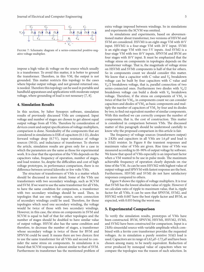
In Figure 7, 𝐶1–𝐶4 consist of the positive section and𝐶5–𝐶8 consist of the negative section of SPNVM. If in thisconfiguration we ground the negative side of the load, it will
Journal of Electrical and Computer Engineering 5
+
C1
C2
C3
C4
C5 C7
C8C6
D1 D2 D3 D4 D5 D6 D7 D8
Rl
Vs
Vo−
Figure 7: Schematic diagram of a series-connected positive-neg-ative voltage multiplier.
impose a high value dc voltage on the source which usuallyis a transformer. To avoid this matter, it is better to groundthe transformer. Therefore, in this VM, the output is notgrounded. This matter restricts this topology to the caseswhere bipolar output voltage, and not ground-returned one,is needed.Therefore this topology can be used in portable andhandheld apparatuses and applications withmoderate outputvoltage, where grounding of load is not nessesary [7, 8].
4. Simulation Results
In this section, by Saber Synopsys software, simulationresults of previously discussed VMs are compared. Inputvoltage and number of stages are chosen to get almost equaloutput voltage from all VMs. Therefore by consideration ofdevices count and output specifications of voltagemultipliers,comparison is done. Nonideality of the components that areconsidered in simulations is ESR of capacitors (0.1Ω), diodesforward voltage drop (0.7 V), input resistance of voltagesources (50Ω), and inductance of transformer. To shortenthe article, simulation results are given only for a case inwhich the parameters are the same as those for experimentalwork. It is clear that the operation of the VMs depends on thecapacitors value, frequency of operation, number of stages,and load resistor. So, despite the difficulties and cost of highvoltage prototypes, in performance comparison, there is nodifference between several kilovolts or few volts VMs.
The structure of transformers of VMs is a matter whichshould be discussed in more detail. Some of the VMs usetransformers with two secondary windings, such as SCVMand SVM. If we want to use the same transformer for all VMs,to have the same condition for comparison, a transformerwith two secondary windings should be used. Then, intopologies that use one voltage source, series connectionof secondary windings could be used. Therefore, for thosetopologies which need one secondary winding, the voltagewould be twice of those with two secondary windings.However, in this case, the stress on components in SVM andSCVM is equal to half of that for other topologies and thenumber of stages should be doubled to have similar valueof output voltage. HSVM also has the same condition andtherefore, to decrease the number of stages, a transformerwhose secondary voltage is twice of those for BVM andSPNVM could be used. It means there are two choices: firstto use the same transformer for all VMs and second to con-sider the same stress on components. In simulations it isfound that SCVM response is almost similar to that of SVM.Furthermore its transformer has the mentioned problem of
extra voltage imposed between windings. So in simulationsand experiments the SCVM was omitted.
In simulations and experiments, based on abovemen-tioned matter about transformer, two versions of HSVM andSVM are considered. HSVM1 is an eight-stage VM with 10Vinput. HSVM2 is a four-stage VM with 20V input. SVM1is an eight-stage VM with two 5V inputs. And SVM2 is afour-stage VM with two 10V inputs. SPNVM and BVM arefour stages with 10V input. It must be emphasized that thevoltage stress on components in topologies depends on thetransformer voltage. That is, the magnitude of voltage stresson HSVM1 and SVM1 components is half of that for others.So in components count we should consider this matter.We know that a capacitor with 𝐶 value and 𝑉𝑏 breakdownvoltage can be built by four capacitors with C value and𝑉𝑏/2 breakdown voltage, that is, parallel connection of twoseries-connected ones. Furthermore two diodes with 𝑉𝑏/2breakdown voltage can build a diode with 𝑉𝑏 breakdownvoltage. Therefore, if the stress on components of VM1 istwice of that for VM2, in components count we can considercapacitors and diodes of VM2 as basic components and mul-tiply the number of capacitors of VM1 by four and its diodesby two, to find out equivalent number of similar components.With this method we can correctly compare the number ofcomponents, that is, the cost of construction. This matteris considered in comparison between VMs. The discussedmatter of this paragraph should be understood carefully toknow why the proposed comparison in this article is fair.
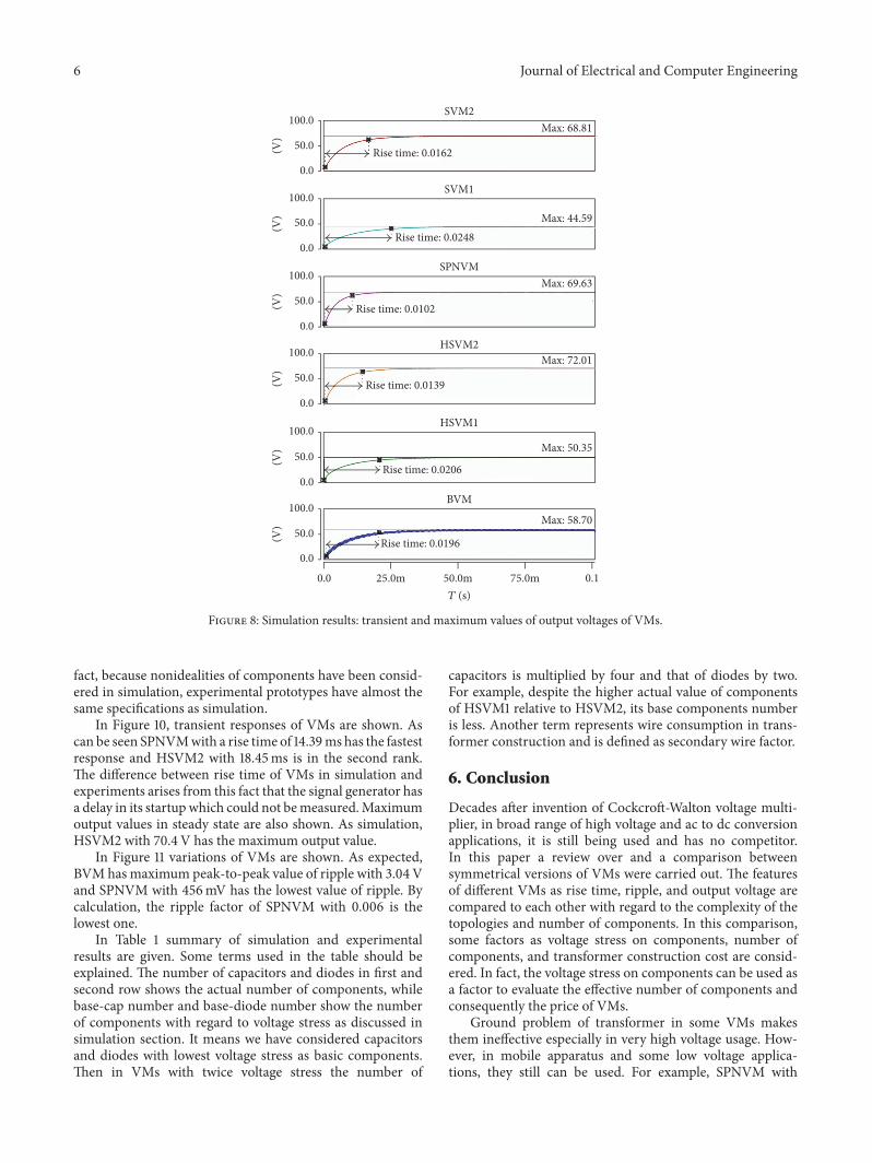
The frequency of voltage sources (transformers output)is 2 KHz and capacitors in all VMs are 1.6 𝜇F and load isa 51 kΩ resistor. In Figure 8 the transient responses andmaximum value of VMs are given. Rise time of VMs wasmeasured according to 10–90% of output voltage by software.We know that speed of VMs especially is an important factorwhen a VM wanted to be use in pulse mode. The maximumachievable frequency of operation clearly depends on risetime of the VM. As can be seen HSVM2 with highest value ofoutput voltage and SPNVMwith fastest response are the best.Furthermore, HSVM1 and SVM1 do not have satisfactoryresponses compared to others.
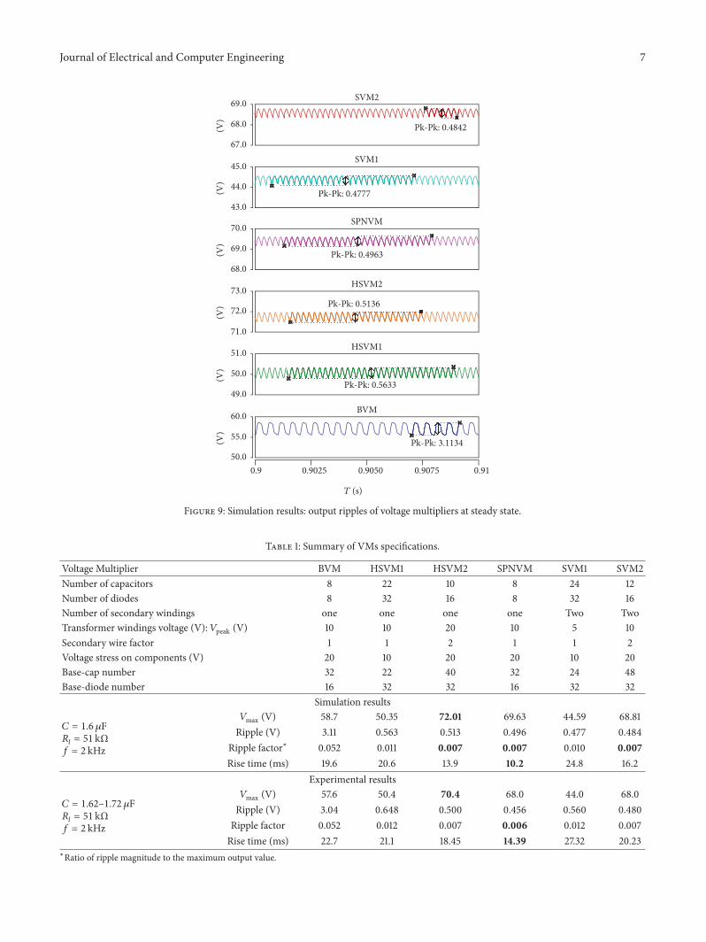
Figure 9 shows the ripples of voltage multipliers. It is truethat SVM1 has the lowest absolute value of ripple. However ifwe calculate ratio of ripple to maximum value, that is, ripplefactor for all VMs, it can be seen that SPNVM, SVM2, andHSVM2 with 0.007 have the best ripple factor and BVM, asexpected, with 0.053 being the worst one.
5. Experimental Comparison
To verify the simulation results, prototypes of VMs havebeen constructed. BVM, SPNVM, HSVM1, HSVM2, SVM1,and SVM2 have been constructed for comparison. Input is a2 kHz sinusoidal source with variable amplitude which com-bined with a ferrite core transformer provides the requestedvoltages. As in simulation a purely resistive 51 kΩ load isused. Capacitors are in range of 1.62𝜇F–1.72 𝜇F and have beenchosen among many, to be nearly equivalent. Reduction oferror produced by nonequal value of capacitors when wecompare the topologies was the reason of such selection. In
6 Journal of Electrical and Computer Engineering
SVM2
SVM1
SPNVM
HSVM2
HSVM1
BVM
0.0
100.0
(V)
(V)
(V)
(V)
(V)
(V)
50.0
0.0
100.0
50.0
0.0
100.0
50.0
0.0
100.0
50.0
0.0
100.0
50.0
0.0
100.0
50.0
0.0
Max: 68.81
Max: 44.59
Max: 69.63
Max: 72.01
Max: 50.35
Max: 58.70
Rise time: 0.0162
Rise time: 0.0248
Rise time: 0.0102
Rise time: 0.0139
Rise time: 0.0206
Rise time: 0.0196
0.1T (s)
25.0m 50.0m 75.0m
Figure 8: Simulation results: transient and maximum values of output voltages of VMs.
fact, because nonidealities of components have been consid-ered in simulation, experimental prototypes have almost thesame specifications as simulation.
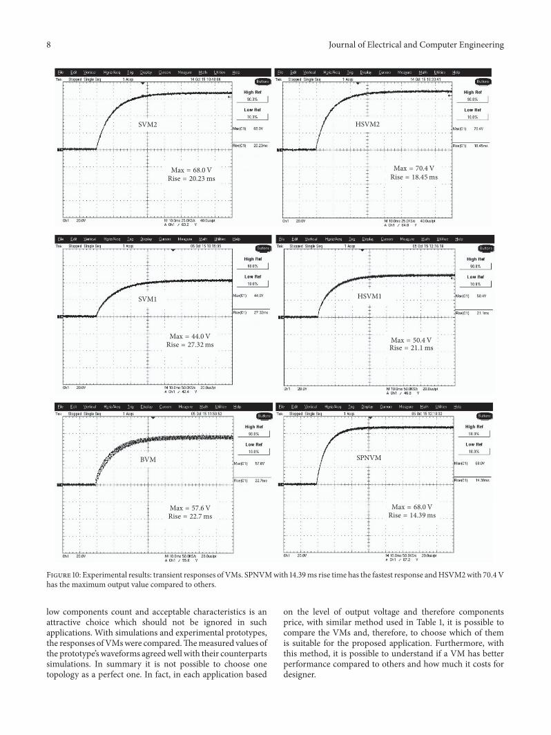
In Figure 10, transient responses of VMs are shown. Ascan be seen SPNVMwith a rise time of 14.39ms has the fastestresponse and HSVM2 with 18.45ms is in the second rank.The difference between rise time of VMs in simulation andexperiments arises from this fact that the signal generator hasa delay in its startupwhich could not bemeasured.Maximumoutput values in steady state are also shown. As simulation,HSVM2 with 70.4V has the maximum output value.
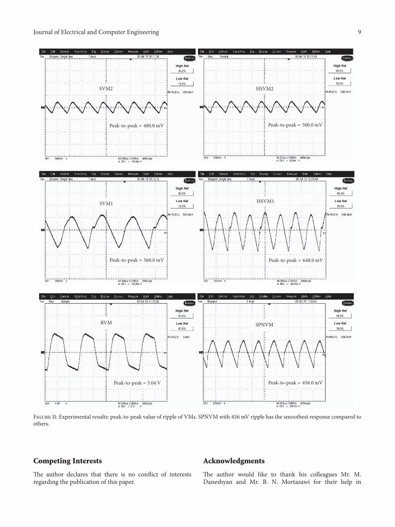
In Figure 11 variations of VMs are shown. As expected,BVM has maximum peak-to-peak value of ripple with 3.04Vand SPNVM with 456mV has the lowest value of ripple. Bycalculation, the ripple factor of SPNVM with 0.006 is thelowest one.
In Table 1 summary of simulation and experimentalresults are given. Some terms used in the table should beexplained. The number of capacitors and diodes in first andsecond row shows the actual number of components, whilebase-cap number and base-diode number show the numberof components with regard to voltage stress as discussed insimulation section. It means we have considered capacitorsand diodes with lowest voltage stress as basic components.Then in VMs with twice voltage stress the number of
capacitors is multiplied by four and that of diodes by two.For example, despite the higher actual value of componentsof HSVM1 relative to HSVM2, its base components numberis less. Another term represents wire consumption in trans-former construction and is defined as secondary wire factor.
6. Conclusion
Decades after invention of Cockcroft-Walton voltage multi-plier, in broad range of high voltage and ac to dc conversionapplications, it is still being used and has no competitor.In this paper a review over and a comparison betweensymmetrical versions of VMs were carried out. The featuresof different VMs as rise time, ripple, and output voltage arecompared to each other with regard to the complexity of thetopologies and number of components. In this comparison,some factors as voltage stress on components, number ofcomponents, and transformer construction cost are consid-ered. In fact, the voltage stress on components can be used asa factor to evaluate the effective number of components andconsequently the price of VMs.
Ground problem of transformer in some VMs makesthem ineffective especially in very high voltage usage. How-ever, in mobile apparatus and some low voltage applica-tions, they still can be used. For example, SPNVM with
Journal of Electrical and Computer Engineering 7
BVM
SVM2
SVM1
SPNVM
HSVM2
HSVM1
69.0
68.0
67.0
45.0
44.0
43.0
70.0
69.0
68.0
73.0
72.0
71.0
51.0
50.0
49.0
60.0
(V)
(V)
(V)
(V)
(V)
(V)
55.0
50.00.9 0.9025 0.9050 0.9075 0.91
Pk-Pk: 0.4842
Pk-Pk: 0.4777
Pk-Pk: 0.4963
Pk-Pk: 0.5136
Pk-Pk: 0.5633
Pk-Pk: 3.1134
T (s)
Figure 9: Simulation results: output ripples of voltage multipliers at steady state.
Table 1: Summary of VMs specifications.
Voltage Multiplier BVM HSVM1 HSVM2 SPNVM SVM1 SVM2Number of capacitors 8 22 10 8 24 12Number of diodes 8 32 16 8 32 16Number of secondary windings one one one one Two TwoTransformer windings voltage (V): 𝑉peak (V) 10 10 20 10 5 10Secondary wire factor 1 1 2 1 1 2Voltage stress on components (V) 20 10 20 20 10 20Base-cap number 32 22 40 32 24 48Base-diode number 16 32 32 16 32 32
Simulation results
𝐶 = 1.6 𝜇F𝑅𝑙 = 51 kΩ𝑓 = 2 kHz
𝑉max (V) 58.7 50.35 72.01 69.63 44.59 68.81Ripple (V) 3.11 0.563 0.513 0.496 0.477 0.484
Ripple factor∗ 0.052 0.011 0.007 0.007 0.010 0.007Rise time (ms) 19.6 20.6 13.9 10.2 24.8 16.2
Experimental results
𝐶 = 1.62–1.72 𝜇F𝑅𝑙 = 51 kΩ𝑓 = 2 kHz
𝑉max (V) 57.6 50.4 70.4 68.0 44.0 68.0Ripple (V) 3.04 0.648 0.500 0.456 0.560 0.480Ripple factor 0.052 0.012 0.007 0.006 0.012 0.007Rise time (ms) 22.7 21.1 18.45 14.39 27.32 20.23
∗Ratio of ripple magnitude to the maximum output value.
8 Journal of Electrical and Computer Engineering
SVM2 HSVM2
SVM1 HSVM1
BVM SPNVM
Max = 68.0 VRise = 20.23 ms
Max = 70.4 VRise = 18.45ms
Max = 44.0 VRise = 27.32ms
Max = 50.4 VRise = 21.1 ms
Max = 57.6 VRise = 22.7 ms
Max = 68.0 VRise = 14.39ms
Figure 10: Experimental results: transient responses of VMs. SPNVMwith 14.39ms rise time has the fastest response andHSVM2with 70.4Vhas the maximum output value compared to others.
low components count and acceptable characteristics is anattractive choice which should not be ignored in suchapplications. With simulations and experimental prototypes,the responses ofVMswere compared.Themeasured values ofthe prototype’s waveforms agreedwell with their counterpartssimulations. In summary it is not possible to choose onetopology as a perfect one. In fact, in each application based
on the level of output voltage and therefore componentsprice, with similar method used in Table 1, it is possible tocompare the VMs and, therefore, to choose which of themis suitable for the proposed application. Furthermore, withthis method, it is possible to understand if a VM has betterperformance compared to others and how much it costs fordesigner.
Journal of Electrical and Computer Engineering 9
SVM2 HSVM2
SVM1 HSVM1
BVM SPNVM
Peak-to-peak = 480.0 mV Peak-to-peak = 500.0 mV
Peak-to-peak = 560.0 mV Peak-to-peak = 648.0 mV
Peak-to-peak = 456.0mVPeak-to-peak = 3.04 V
Figure 11: Experimental results: peak-to-peak value of ripple of VMs. SPNVM with 456mV ripple has the smoothest response compared toothers.
Competing Interests
The author declares that there is no conflict of interestsregarding the publication of this paper.
Acknowledgments
The author would like to thank his colleagues Mr. M.Daneshyan and Mr. B. N. Mortazawi for their help in
10 Journal of Electrical and Computer Engineering
preparing experimental tests. This work was supported byproject from “Laser & Optics Research School” (Code no.PRD-L2-93-007).
References
[1] S. Iqbal, “A hybrid symmetrical voltage multiplier,” IEEE Trans-actions on Power Electronics, vol. 29, no. 1, pp. 6–12, 2014.
[2] S. Iqbal, R. Besar, and C. Venkataseshaiah, “Single/three-phasesymmetrical bipolar voltagemultipliers forX-ray power supply,”in Proceedings of the 2nd International Conference on ElectricalEngineering (ICEE ’08), pp. 1–6, IEEE, Lahore, Pakistan, March2008.
[3] C.-M. Young, M.-H. Chen, S.-H. Yeh, and K.-H. Yuo, “A Single-phase single-stage high step-UpAC-DCmatrix converter basedon cockcroft-walton voltage multiplier with PFC,” IEEE Trans-actions on Power Electronics, vol. 27, no. 12, pp. 4894–4905, 2012.
[4] T.-L. Su, Y.-M. Zhang, S.-W. Chen, Y.-T. Liu, H.-Y. Lv, and J.-T.Liu, “A 600kV 15mACockcroft-Walton high-voltage power sup-ply with high stability and low-ripple voltage,” Nuclear Instru-ments and Methods in Physics Research Section A: Accelerators,Spectrometers, Detectors and Associated Equipment, vol. 560, no.2, pp. 613–616, 2006.
[5] Z.-F. He, J.-L. Zhang, Y.-H. Liu, Y.-T. Zhang, and Y. Zhang,“Characteristics of a symmetrical Cockcroft-Walton powersupply of 50Hz 1.2MV/50mA,”Review of Scientific Instruments,vol. 82, no. 5, Article ID 055116, 2011.
[6] C.-M.Young,H.-L. Chen, andM.-H.Chen, “A cockcroft-waltonvoltage multiplier fed by a three-phase-to-single-phase matrixconverter with PFC,” IEEE Transactions on Industry Applica-tions, vol. 50, no. 3, pp. 1994–2004, 2014.
[7] D. F. Spencer, R. Aryaeinejad, and E. L. Reber, “Using the Cock-roft-Walton voltage multiplier with small photomultipliers,”IEEE Transactions on Nuclear Science, vol. 49, no. 3, pp. 1152–1155, 2002.
[8] D. F. Spencer, R. Aryaeinejad, and E. L. Reber, “Using thecockcroft-walton voltage multiplier design in handheld devi-ces,” in Proceedings of the IEEENuclear Science SymposiumCon-ference Record, pp. 746–749, San Diego, Calif, USA, November2001.
[9] M. Rezanejad, A. Sheikholeslami, and J. Adabi, “High-voltagepulsed power supply to generate wide pulses combined withnarrow pulses,” IEEE Transactions on Plasma Science, vol. 42,no. 7, pp. 1894–1901, 2014.
[10] L.Muller and J.W.Kimball, “Dual-input high gainDC-DC con-verter based on the cockcroft-walton multiplier,” in Proceedingsof the IEEE Energy Conversion Congress and Exposition (ECCE’14), pp. 5360–5367, IEEE, Pittsburgh, Pa, USA, September 2014.
[11] Z. Cao, M. Hu, N. Frohleke, and J. Bocker, “Modeling and con-trol design for a very low-frequency high-voltage test system,”IEEE Transactions on Power Electronics, vol. 25, no. 4, pp. 1068–1077, 2010.
[12] E. Everhart and P. Lorrain, “The Cockcroft−Walton voltagemultiplying circuit,” Review of Scientific Instruments, vol. 24, no.3, pp. 221–226, 1953.
[13] G. Reinhold, K. Truempy, and J. Bill, “The symmetrical cascaderectifier an accelerator power supply in the megavolt and mil-liampere range,” IEEE Transactions on Nuclear Science, vol. 12,no. 3, pp. 288–292, 1965.
[14] S. Iqbal, “A three-phase symmetrical multistage voltage multi-plier,” IEEE Power Electronics Letters, vol. 3, no. 1, pp. 30–33,2005.
[15] M. Abdel-Salam,High-Voltage Engineering:Theory and Practice,Revised and Expanded, CRC Press, Boca Raton, Fla, USA, 2000.
[16] J. Kuffel, E. Kuffel, and W. S. Zaengl, High Voltage EngineeringFundamentals, Newnes, 2000.
[17] C. L. Wadhwa, High Voltage Engineering, New Age Interna-tional, New Delhi, India, 2007.
[18] C. G. H. Maennel, “Improvement in the modelling of a half-wave Cockroft-Walton voltage multiplier,” Review of ScientificInstruments, vol. 84, no. 6, Article ID 064701, 2013.
[19] I. C. Kobougias and E. C. Tatakis, “Optimal design of a half-wave Cockcroft–Walton voltage multiplier with minimum totalcapacitance,” IEEETransactions onPower Electronics, vol. 25, no.9, pp. 2460–2468, 2010.
[20] F. Hwang, Y. Shen, and S. H. Jayaram, “Low-ripple compacthigh-voltage DC power supply,” IEEE Transactions on IndustryApplications, vol. 42, no. 5, pp. 1139–1145, 2006.
[21] H. Zhang and A. Takaoka, “Ripple due to asymmetry in sym-metrical Cockcroft–Walton cascade rectifier circuit,” Review ofScientific Instruments, vol. 65, no. 12, pp. 3864–3865, 1994.
[22] H. Zhang and A. Takaoka, “Fundamental harmonic of ripplesin symmetrical Cockcroft-Walton cascade rectifying circuit,”Review of Scientific Instruments, vol. 67, no. 9, pp. 3336–3337,1996.
[23] S. Iqbal and R. Besar, “A bipolar Cockcroft-Walton VoltageMul-tiplier for gas lasers,” American Journal of Applied Sciences, vol.4, no. 10, pp. 795–801, 2007.

International Journal of
AerospaceEngineeringHindawi Publishing Corporationhttp://www.hindawi.com Volume 2014
RoboticsJournal of
Hindawi Publishing Corporationhttp://www.hindawi.com Volume 2014
Hindawi Publishing Corporationhttp://www.hindawi.com Volume 2014
Active and Passive Electronic Components
Control Scienceand Engineering
Journal of
Hindawi Publishing Corporationhttp://www.hindawi.com Volume 2014
International Journal of
RotatingMachinery
Hindawi Publishing Corporationhttp://www.hindawi.com Volume 2014
Hindawi Publishing Corporation http://www.hindawi.com
Journal ofEngineeringVolume 2014
Submit your manuscripts athttps://www.hindawi.com
VLSI Design
Hindawi Publishing Corporationhttp://www.hindawi.com Volume 2014
Hindawi Publishing Corporationhttp://www.hindawi.com Volume 2014
Shock and Vibration
Hindawi Publishing Corporationhttp://www.hindawi.com Volume 2014
Civil EngineeringAdvances in
Acoustics and VibrationAdvances in
Hindawi Publishing Corporationhttp://www.hindawi.com Volume 2014
Hindawi Publishing Corporationhttp://www.hindawi.com Volume 2014
Electrical and Computer Engineering
Journal of
Advances inOptoElectronics
Hindawi Publishing Corporation http://www.hindawi.com
Volume 2014
The Scientific World JournalHindawi Publishing Corporation http://www.hindawi.com Volume 2014
SensorsJournal of
Hindawi Publishing Corporationhttp://www.hindawi.com Volume 2014
Modelling & Simulation in EngineeringHindawi Publishing Corporation http://www.hindawi.com Volume 2014
Hindawi Publishing Corporationhttp://www.hindawi.com Volume 2014
Chemical EngineeringInternational Journal of Antennas and
Propagation
International Journal of
Hindawi Publishing Corporationhttp://www.hindawi.com Volume 2014
Hindawi Publishing Corporationhttp://www.hindawi.com Volume 2014
Navigation and Observation
International Journal of
Hindawi Publishing Corporationhttp://www.hindawi.com Volume 2014
DistributedSensor Networks
International Journal of