![Chapter 5 SPACE VECTOR PWM - · PDF file175 Chapter 5 SPACE VECTOR PWM 5.1 5.2 Introduction The space vector PWM (SVPWM) [5.1] is an alternative method used to control three](https://static.fdocuments.us/doc/165x107/5a76cdea7f8b9a1b688d899f/chapter-5-space-vector-pwm-fleadh-175-chapter-5-space-vector-pwm-51-52-introduction.jpg)
A Comparative Study of Different Approaches Presents in ... · The PWM technique termed as Space...
18
International Journal of Emerging Engineering Research and Technology Volume 2, Issue 5, August 2014, PP 1-18 ISSN 2349-4395 (Print) & ISSN 2349-4409 (Online) ©IJEERT www.ijeert.org 1 A Comparative Study of Different Approaches Presents in Two Level Space Vector Pulse Width Modulated Three Phase Voltage Source Invertes S. Manivannan, K. Senthilnathan, P. Selvabharathi, K.Rajalashmi Department of Electrical and Electronics Engineering, Bannari Amman Institute of Technology, Erode, Tamilnadu, India Abstract: The Three Phase Voltage Source Inverter supplies invariably required variable voltage and frequency of the adjustable speed drive system. A number of pulse width modulation (PWM) schemes are used to obtain variable voltage and frequency supply from an inverter. The most widely used PWM scheme for a Three Phase Voltage Source Inverter is carrier based sinusoidal PWM and Space Vector Pulse Width Modulation (SVPWM). There is an increasing trend of using SVPWM, because of their easier digital realization and better DC bus utilization. The study of SVPWM technique reveals that this technique utilizes DC bus voltage more efficiently and generates less harmonic distortion when compared with sinusoidal PWM techniques. The SVPWM technique has become one of the important PWM technique for Three Phase Voltage Source Inverter for the control of AC induction motor, Brushless DC motor, Switched Reluctance motor and Permanent Magnet Synchronous motor. In this paper having collection of different schemes in SVPWM. Specifically various schemes are carrier waveform based modulated reference waveform generation and comparison in SVPWM, Center aligned two level SVPWM, Edge align based sampled reference frame generation in SVPWM, Level shifted multi-carrier concepts based SVPWM and Third order harmonic injection based modulated reference waveform generation and comparison in SVPWM. This paper having simulation results of all the five schemes of SVPWM by using MATLAB/SIMULINK software. The performance of Three Phase Voltage Source Inverter based on various SVPWM schemes are analyzed by various reference parameters like DC bus utilization, Total harmonic distortion (THD), switching stress and efficiency. As a result of these analysis this paper recommends which scheme is more suitable for variable voltage and various frequency drives. The simulation results are provided to validate the proposed model approaches. Keywords: Three Phase Voltage Source Inverter, Space vector Pulse width Modulation (SVPWM), Modulated reference waveform, Center aligned, Edge aligned, Total Harmonic Distortion (THD), Switching Stress. 1. INTRODUCTION Three phase voltage source inverters are widely used in variable speed AC motor drive applications since they provide variable voltage and variable frequency output through pulse width modulation control [1] [2]. The most widely used PWM method is the carrier-based sine-triangle PWM method due to simple implementation in both analog and digital realization [2] [3]. However in this method the DC bus utilization is low (0.5V dc ). This has led to the investigation into other techniques with an objective of improving in the DC bus utilization [1] [3]. The PWM technique termed as Space Vector PWM based on space vector theory was proposed by de Broeck et. Al (1988) and Ogasawara et.al (1989) which offers superior performance compared to the carrier –based sine-triangle PWM technique I terms of higher DC bus utilization and better harmonics performance [3]. Further, this technique offers easier digital realization. The research in PWM schemes has intensified in the last few decades. The main aim of any modulation technique is to obtain a variable output with a maximum fundamental component and minimum harmonics [3] [4]. The problem of underutilization of the DC bus voltage led to the development of the Third harmonic- injection PWM (THIPWM) and Space Vector PWM (SVPWM) [5] [6]. In 1975, Buja developed this improved sinusoidal PWM technique which added a third –order harmonic content in the sinusoidal reference signal leading to a 15.5% increase in the utilization rate of the DC bus voltage. In 1988, Van Der Broeck developed the SVPWM technique which has also increased the utilization of DC bus voltage by 15.5% [7] [8].
Transcript of A Comparative Study of Different Approaches Presents in ... · The PWM technique termed as Space...

International Journal of Emerging Engineering Research and Technology
Volume 2, Issue 5, August 2014, PP 1-18
ISSN 2349-4395 (Print) & ISSN 2349-4409 (Online)
©IJEERT www.ijeert.org 1
A Comparative Study of Different Approaches Presents in Two
Level Space Vector Pulse Width Modulated Three Phase Voltage
Source Invertes
S. Manivannan, K. Senthilnathan, P. Selvabharathi, K.Rajalashmi
Department of Electrical and Electronics Engineering,
Bannari Amman Institute of Technology, Erode, Tamilnadu, India
Abstract: The Three Phase Voltage Source Inverter supplies invariably required variable voltage and
frequency of the adjustable speed drive system. A number of pulse width modulation (PWM) schemes are used
to obtain variable voltage and frequency supply from an inverter. The most widely used PWM scheme for a
Three Phase Voltage Source Inverter is carrier based sinusoidal PWM and Space Vector Pulse Width
Modulation (SVPWM). There is an increasing trend of using SVPWM, because of their easier digital realization
and better DC bus utilization. The study of SVPWM technique reveals that this technique utilizes DC bus
voltage more efficiently and generates less harmonic distortion when compared with sinusoidal PWM techniques. The SVPWM technique has become one of the important PWM technique for Three Phase Voltage
Source Inverter for the control of AC induction motor, Brushless DC motor, Switched Reluctance motor and
Permanent Magnet Synchronous motor. In this paper having collection of different schemes in SVPWM.
Specifically various schemes are carrier waveform based modulated reference waveform generation and
comparison in SVPWM, Center aligned two level SVPWM, Edge align based sampled reference frame
generation in SVPWM, Level shifted multi-carrier concepts based SVPWM and Third order harmonic injection
based modulated reference waveform generation and comparison in SVPWM. This paper having simulation
results of all the five schemes of SVPWM by using MATLAB/SIMULINK software. The performance of Three
Phase Voltage Source Inverter based on various SVPWM schemes are analyzed by various reference
parameters like DC bus utilization, Total harmonic distortion (THD), switching stress and efficiency. As a result
of these analysis this paper recommends which scheme is more suitable for variable voltage and various
frequency drives. The simulation results are provided to validate the proposed model approaches.
Keywords: Three Phase Voltage Source Inverter, Space vector Pulse width Modulation (SVPWM), Modulated
reference waveform, Center aligned, Edge aligned, Total Harmonic Distortion (THD), Switching Stress.
1. INTRODUCTION
Three phase voltage source inverters are widely used in variable speed AC motor drive applications
since they provide variable voltage and variable frequency output through pulse width modulation
control [1] [2]. The most widely used PWM method is the carrier-based sine-triangle PWM method due to simple implementation in both analog and digital realization [2] [3]. However in this method
the DC bus utilization is low (0.5Vdc). This has led to the investigation into other techniques with an
objective of improving in the DC bus utilization [1] [3]. The PWM technique termed as Space Vector PWM based on space vector theory was proposed by de Broeck et. Al (1988) and Ogasawara et.al
(1989) which offers superior performance compared to the carrier –based sine-triangle PWM
technique I terms of higher DC bus utilization and better harmonics performance [3]. Further, this
technique offers easier digital realization. The research in PWM schemes has intensified in the last few decades. The main aim of any modulation technique is to obtain a variable output with a
maximum fundamental component and minimum harmonics [3] [4].
The problem of underutilization of the DC bus voltage led to the development of the Third harmonic-injection PWM (THIPWM) and Space Vector PWM (SVPWM) [5] [6]. In 1975, Buja developed this
improved sinusoidal PWM technique which added a third –order harmonic content in the sinusoidal
reference signal leading to a 15.5% increase in the utilization rate of the DC bus voltage. In 1988, Van
Der Broeck developed the SVPWM technique which has also increased the utilization of DC bus voltage by 15.5% [7] [8].

S. Manivannan et al.
International Journal of Emerging Engineering Research and Technology 2
In the last three decades there are different SVPWM schemes are developed by various authors. But
this paper is mainly focus on important five schemes in SVPWM. The various schemes in SVPWM are a) Carrier waveform based modulated reference waveform generation and comparison in
SVPWM, b) Center aligned two level SVPWM, c) Edge align based sampled reference frame
generation in SVPWM, d) Level shifted multi-carrier concepts based SVPWM and e) Third order harmonic injection based modulated reference waveform generation and comparison in SVPWM.
Here these five techniques have similar results, but their methods of implementation are completely
different. With the development of microprocessors SVPWM has become one of the most important PWM methods for three phase inverter. The maximum peak fundamental magnitude of the SVPWM
technique is about 90.6% increase in the maximum voltage compared with conventional sinusoidal
modulation [12]- [16].
This paper having some collective information regarding various schemes as mentioned above presents in the two level SVPWM based Three Phase Voltage Source Inverter. This paper covers
entire concepts presents in all the five schemes and also this paper gives a comparative statement
regarding all those five schemes. The comparative statement is developed by the following valuable parameters. The parameters are THD, DC bus utilization, switching stress and efficiency. As a result
of this comparative statement the reader can identify which scheme is more suitable for particular
drive operation. The simulation results are provided to validate the proposed approaches. The paper
organized in ten sections. Section II gives some basic introduction regarding SVPWM techniques. Section III introduces the detailed discussion regarding Third order harmonic injection based
modulated reference waveform generation and comparison in SVPWM. Section IV introduces the
detailed discussion regarding Edge align based sampled reference frame generation in SVPWM. Section V introduces the detailed discussion regarding Carrier waveform based modulated reference
waveform generation and comparison in SVPWM. Section VI introduces the detailed discussion
regarding Center aligned two level SVPWM. Section VII introduces the detailed discussion regarding Level shifted multi-carrier concepts based SVPWM. Section VIII gives the detailed comparison
between the above mentioned schemes. Section IX shows the extension of the proposed scheme to the
Z- source and T- source inverters. Section X concludes the paper.
2. SVPWM PRINCIPLE’S
Space Vector Modulation (SVM) was originally developed as a vector approach to pulse width
modulation (PWM) for three phase inverter. It is a more sophisticated technique for generating sine wave that provides a higher voltage to the motor with lower harmonic distortion [13]. The main aim
of any modulation technique is to obtain variable output having a maximum fundamental component
with minimum harmonics. SVPWM method is an advance: computation intensive PWM method and
possibly the best techniques for variable frequency drive applications.
The principle of pulse width modulation is explained by using the figure-1 [22]. The figure-1 (a)
shows a circuit model of a single phase inverter with a center-tapped grounded DC bus. The figure-1
(b) illustrates principles of pulse width modulation.
Figure-1 (a) circuit model of a single phase inverter, Figure-1 (b) pulse width modulation
From the figure-1 (b), the inverter output voltage is determined by the following ways.
1. When V control > V triangle means VAO = VDC/2 2. When V control < V triangle means VAO = -VDC/2
A Comparative Study of Different Approaches Presents in Two Level Space Vector Pulse Width
Modulated Three Phase Voltage Source Invertes
International Journal of Emerging Engineering Research and Technology 3
Also the inverter output voltage has the following features. 1. PWM frequency as same as the V triangle frequency.
2. Amplitude is controlled by the peak value of V triangle.
3. The fundamental frequency is controlled by the frequency of V control.
4. Modulation index (M) is defined as
VcontrolM
Vtriangle; 0 ≤ M ≤ 1
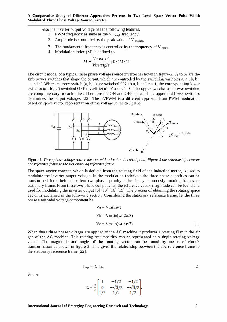
The circuit model of a typical three phase voltage source inverter is shown in figure-2. S1 to S6 are the
sin's power switches that shape the output, which are controlled by the switching variables a, a’, b, b’,
c, and c’. When an upper switch (a, b, c) are switched ON ie) a, b and c = 1, the corresponding lower switches (a’, b’, c’) switched OFF myself ie) a’, b’ and c’ = 0. The upper switches and lower switches
are complimentary to each other. Therefore the ON and OFF states of the upper and lower switches
determines the output voltages [22]. The SVPWM is a different approach from PWM modulation based on space vector representation of the voltage in the α-β plane.
Figure-2. Three phase voltage source inverter with a load and neutral point, Figure-3 the relationship between
abc reference frame to the stationary dq reference frame
The space vector concept, which is derived from the rotating field of the induction motor, is used to
modulate the inverter output voltage. In the modulation technique the three phase quantities can be
transformed into their equivalent two-phase quantity either in synchronously rotating frames or
stationary frame. From these two-phase components, the reference vector magnitude can be found and used for modulating the inverter output [6] [13] [16] [19]. The process of obtaining the rotating space
vector is explained in the following section. Considering the stationary reference frame, let the three
phase sinusoidal voltage component be
Va = Vmsinwt
Vb = Vmsin(wt-2π/3)
Vc = Vmsin(wt-4π/3) [1]
When these three phase voltages are applied to the AC machine it produces a rotating flux in the air
gap of the AC machine. This rotating resultant flux can be represented as a single rotating voltage vector. The magnitude and angle of the rotating vector can be found by means of clark’s
transformation as shown in figure-3. This gives the relationship between the abc reference frame to
the stationary reference frame [22].
f dqo = Ks fabc [2]
Where
Ks = ,

S. Manivannan et al.
International Journal of Emerging Engineering Research and Technology 4
f dqo = T,
fabc=T
and “f” denotes either a voltage or a current variable.
The relationship between the switching variable vector [a b c] T
and the line-to-line voltage vector [Vab
Vbc Vca] T is given by
= Vdc [3]
Also the relationship between the switching variable vector [a b c] T and the phase voltage vector [Van
Vbn Vcn] T
is given by
= [4]
Table-1. Switching vectors, Phase voltages and Output Line to Line voltages
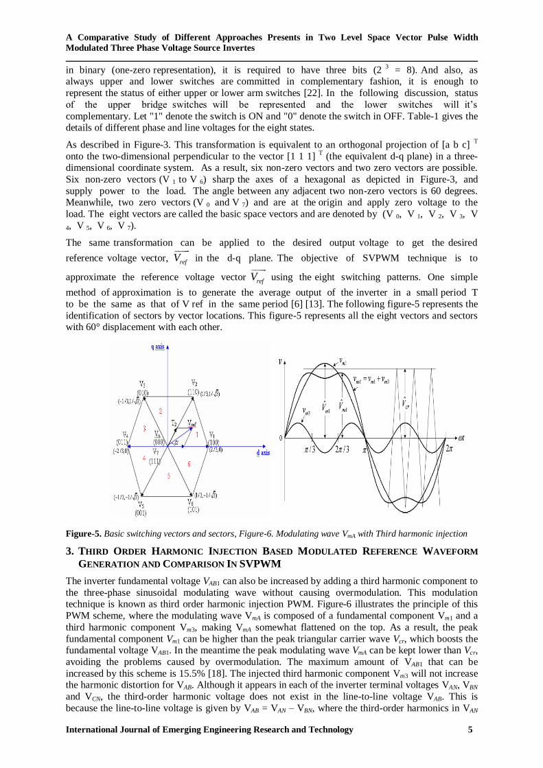
Figure-4. The eight inverter voltage vectors (Vo to V7)
By referring the figure-2 there are eight possible switching combinations of ON and OFF patterns for
the three upper power switches. The ON and OFF states of the lower power devices are opposite to the upper one and so are easily determined once the states of the upper power switches are
determined. According to equation-3 and 4, the eight switching vectors, output line to neutral voltage
(phase voltage), and output line to line voltages in turns of DC link Vdc are given in the table-1. The figure-4 shows the eight inverter voltage vectors (V0 to V7).
For 180° mode of operation, there exist six switching states and additionally two more states,
which make all three switches of either upper arms or lower arms ON. To code these eight states
A Comparative Study of Different Approaches Presents in Two Level Space Vector Pulse Width
Modulated Three Phase Voltage Source Invertes
International Journal of Emerging Engineering Research and Technology 5
in binary (one-zero representation), it is required to have three bits (2 3 = 8). And also, as
always upper and lower switches are committed in complementary fashion, it is enough to
represent the status of either upper or lower arm switches [22]. In the following discussion, status
of the upper bridge switches will be represented and the lower switches will it’s
complementary. Let "1" denote the switch is ON and "0" denote the switch in OFF. Table-1 gives the details of different phase and line voltages for the eight states.
As described in Figure-3. This transformation is equivalent to an orthogonal projection of [a b c] T
onto the two-dimensional perpendicular to the vector [1 1 1] T (the equivalent d-q plane) in a three-
dimensional coordinate system. As a result, six non-zero vectors and two zero vectors are possible.
Six non-zero vectors (V 1 to V 6) sharp the axes of a hexagonal as depicted in Figure-3, and
supply power to the load. The angle between any adjacent two non-zero vectors is 60 degrees. Meanwhile, two zero vectors (V 0 and V 7) and are at the origin and apply zero voltage to the
load. The eight vectors are called the basic space vectors and are denoted by (V 0, V 1, V 2, V 3, V
4, V 5, V 6, V 7).
The same transformation can be applied to the desired output voltage to get the desired
reference voltage vector, refV
in the d-q plane. The objective of SVPWM technique is to
approximate the reference voltage vector refV
using the eight switching patterns. One simple
method of approximation is to generate the average output of the inverter in a small period T
to be the same as that of V ref in the same period [6] [13]. The following figure-5 represents the
identification of sectors by vector locations. This figure-5 represents all the eight vectors and sectors with 60° displacement with each other.
Figure-5. Basic switching vectors and sectors, Figure-6. Modulating wave VmA with Third harmonic injection
3. THIRD ORDER HARMONIC INJECTION BASED MODULATED REFERENCE WAVEFORM
GENERATION AND COMPARISON IN SVPWM
The inverter fundamental voltage VAB1 can also be increased by adding a third harmonic component to
the three-phase sinusoidal modulating wave without causing overmodulation. This modulation technique is known as third order harmonic injection PWM. Figure-6 illustrates the principle of this
PWM scheme, where the modulating wave VmA is composed of a fundamental component Vm1 and a
third harmonic component Vm3, making VmA somewhat flattened on the top. As a result, the peak
fundamental component Vm1 can be higher than the peak triangular carrier wave Vcr, which boosts the fundamental voltage VAB1. In the meantime the peak modulating wave VmA can be kept lower than Vcr,
avoiding the problems caused by overmodulation. The maximum amount of VAB1 that can be
increased by this scheme is 15.5% [18]. The injected third harmonic component Vm3 will not increase the harmonic distortion for VAB. Although it appears in each of the inverter terminal voltages VAN, VBN
and VCN, the third-order harmonic voltage does not exist in the line-to-line voltage VAB. This is
because the line-to-line voltage is given by VAB = VAN – VBN, where the third-order harmonics in VAN
S. Manivannan et al.
International Journal of Emerging Engineering Research and Technology 6
and VBN are of zero sequence with the same magnitude and phase displacement and thus cancel each
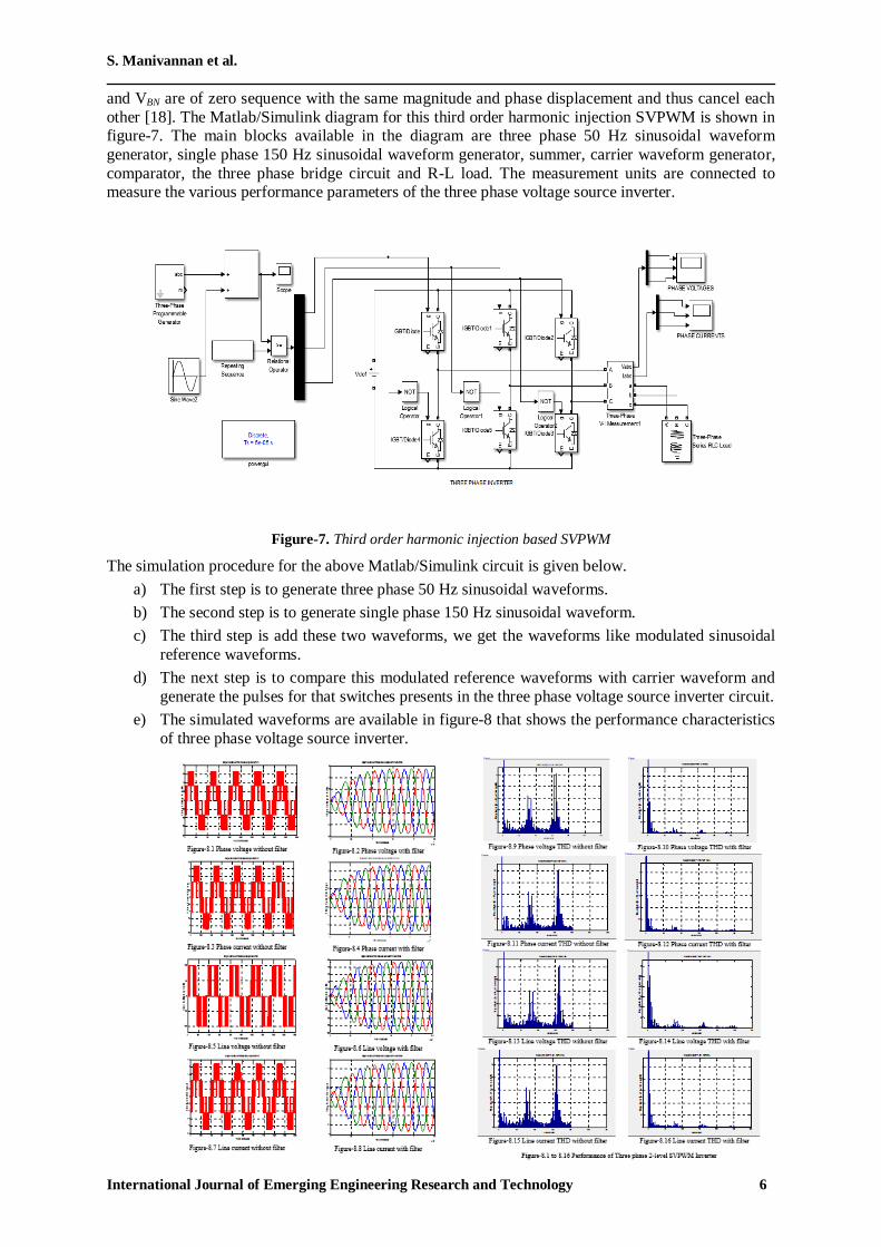
other [18]. The Matlab/Simulink diagram for this third order harmonic injection SVPWM is shown in figure-7. The main blocks available in the diagram are three phase 50 Hz sinusoidal waveform
generator, single phase 150 Hz sinusoidal waveform generator, summer, carrier waveform generator,
comparator, the three phase bridge circuit and R-L load. The measurement units are connected to measure the various performance parameters of the three phase voltage source inverter.
Figure-7. Third order harmonic injection based SVPWM
The simulation procedure for the above Matlab/Simulink circuit is given below.
a) The first step is to generate three phase 50 Hz sinusoidal waveforms.
b) The second step is to generate single phase 150 Hz sinusoidal waveform.
c) The third step is add these two waveforms, we get the waveforms like modulated sinusoidal
reference waveforms.
d) The next step is to compare this modulated reference waveforms with carrier waveform and
generate the pulses for that switches presents in the three phase voltage source inverter circuit.
e) The simulated waveforms are available in figure-8 that shows the performance characteristics
of three phase voltage source inverter.

A Comparative Study of Different Approaches Presents in Two Level Space Vector Pulse Width
Modulated Three Phase Voltage Source Invertes
International Journal of Emerging Engineering Research and Technology 7
4. EDGE ALIGN BASED SAMPLED REFERENCE FRAME GENERATION IN SVPWM
A pulse width modulation (PWM) scheme for two level inverters is proposed. The proposed PWM
scheme generates the inverter leg switching times, from the sampled reference phase voltage
amplitudes and centre the switching times for the middle vectors, in a sampling interval, as in the case of conventional space vector PWM (SVPWM). The SVPWM scheme, presented for multilevel
inverters, can also work in the overmodulation range, using only the sampled amplitudes of reference
phase voltages. The present PWM technique does not involve any sector identification and considerably reduces the computation time when compared to the conventional space vector PWM
technique [14]. The present PWM signal generation scheme can be used for any multilevel inverter
configuration. A two-level inverter configuration, using on R-L load is used to verify the SVPWM
generation scheme experimentally. The figure-9 represents Matlab/Simulink module of the Edge align based sampled reference frame generation in SVPWM.
Figure-9. Edge align based sampled reference frame generation in SVPWM
The simulation procedure for the above Matlab/Simulink circuit is given below.
a) The first step is to generate three phase sinusoidal waveforms with magnitude=1V.
b) The second step is calculate Vmax, Vmin and Vmid.
c) The third step is to calculate the switching time T1, T2, Teff, T0 and Toff.
1 max
2 min
max min
0
0min
2
mid
mid
eff
s eff
off
T V V
T V V
T V V
T T T
TT T
[5]
Where
Vmax – Maximum voltage at the instant of any time in seconds
Vmin – Minimum voltage at the instant of any time in seconds
Vmid – Average voltage at the instant of any time in seconds
T1 – Switch-1 turn ON time period in seconds
S. Manivannan et al.
International Journal of Emerging Engineering Research and Technology 8
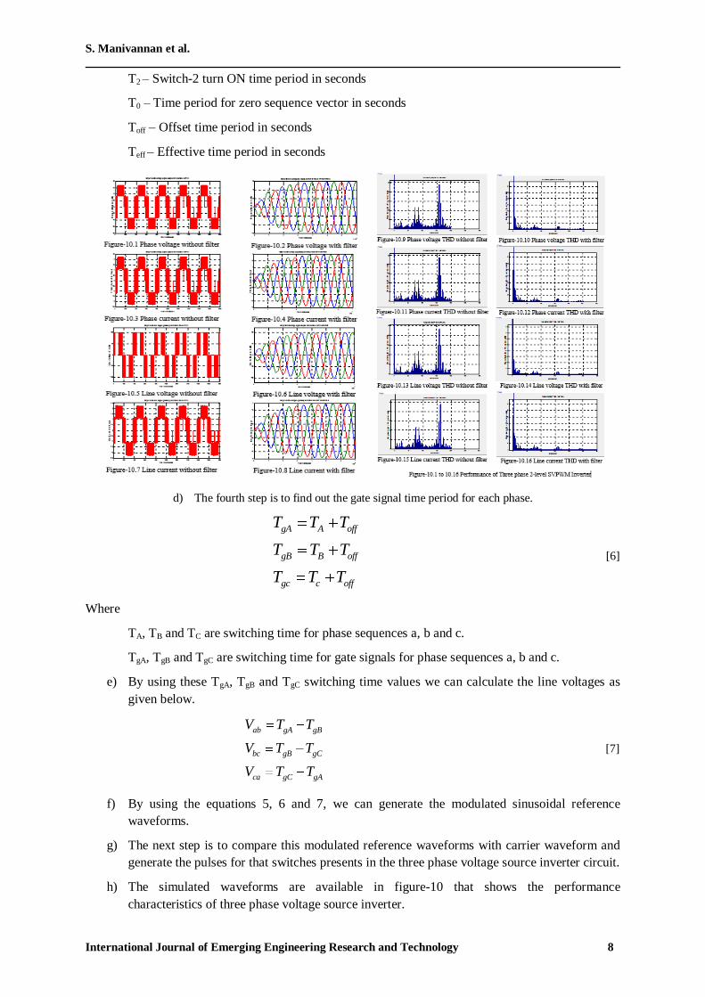
T2 – Switch-2 turn ON time period in seconds
T0 – Time period for zero sequence vector in seconds
Toff – Offset time period in seconds
Teff – Effective time period in seconds
d) The fourth step is to find out the gate signal time period for each phase.
gA A off
gB B off
gc c off
T T T
T T T
T T T
[6]
Where
TA, TB and TC are switching time for phase sequences a, b and c.
TgA, TgB and TgC are switching time for gate signals for phase sequences a, b and c.
e) By using these TgA, TgB and TgC switching time values we can calculate the line voltages as
given below.
ab gA gB
bc gB gC
ca gC gA
V T T
V T T
V T T
[7]
f) By using the equations 5, 6 and 7, we can generate the modulated sinusoidal reference
waveforms.
g) The next step is to compare this modulated reference waveforms with carrier waveform and
generate the pulses for that switches presents in the three phase voltage source inverter circuit.
h) The simulated waveforms are available in figure-10 that shows the performance
characteristics of three phase voltage source inverter.

A Comparative Study of Different Approaches Presents in Two Level Space Vector Pulse Width
Modulated Three Phase Voltage Source Invertes
International Journal of Emerging Engineering Research and Technology 9
5. CARRIER WAVEFORM BASED MODULATED REFERENCE WAVEFORM GENERATION AND
COMPARISON IN SVPWM
There is an increasing trend of using space vector pulse-width modulation (SVPWM) schemes for driving voltage source inverters because of their easier digital realization and better DC bus
utilization.
Figure-11. Carrier waveform based modulated reference waveform generation and comparison in SVPWM
This paper introduces an carrier waveform based modulated reference waveform generation and comparison in SVPWM technique as shown in figure-11 based on a reduced computation method,
which is much simpler and more executable than conventional means without lookup tables or
complex logical judgments. The SVPWM scheme is modeled and simulated using
MATLAB/SIMULINK and experimentally implemented and verified. The simulation procedure for the above Matlab/Simulink circuit is given below.
a) The first step is to generate three phase sinusoidal waveforms with magnitude = 0.8V.
Va = Vmsinwt
Vb = Vmsin(wt-2π/3)
Vc = Vmsin(wt-4π/3)
b) The second step is to find out the maximum value and minimum value among these three
waveforms by using minmax block in Matlab/Simulink.
c) The third step is to add the maximum and minimum values getting from step-2.
d) The fourth step is, divide the values getting from step-3 by -2. Because the magnitude values
of waveform get reduced and the waveforms get opposite polarity.
e) The next step having steps
a. For phase “a” add Va with step-4 waveform
b. For phase “b” add Vb with step-4 waveform
c. For phase “c” add Vc with step-4 waveform
i) The last step is to compare step-5 waveforms with respect to carrier waveform and generates
the pulses for that switch presents in the three phase voltage source inverter circuit.
f) The simulated waveforms are available in figure-12 that shows the performance characteristics of three phase voltage source inverter.

S. Manivannan et al.
International Journal of Emerging Engineering Research and Technology 10
6. CENTER ALIGNED TWO LEVEL SVPWM
By referring the above introductory parts, the SVPWM can be implemented in the following steps.
The first step is to generate three phase waveforms Va, Vb, Vc by referring the equation 1.
Va = Vmsinwt
Vb = Vmsin(wt-2π/3)
Vc = Vmsin(wt-4π/3)
Where w = 2πf and f = 50Hz.
The second step is transforms abc parameters into dq parameters
cos0 cos120 cos 2402 2
b cd a b c a
V VV V V V V
3 3cos 270 cos30 cos150 0
2 2
b cq a b c
V VV V V V
1 11
2 2
2 3 30
3 2 2
0 0 0
a
d
b
qc
VV
VV
V
[8]
The third step is to calculate Vref magnitude and angle (α) values from equation 8.
2 2
1tan
ref d q d q
q
d
V V jV V V
V
V
[9]
A Comparative Study of Different Approaches Presents in Two Level Space Vector Pulse Width
Modulated Three Phase Voltage Source Invertes
International Journal of Emerging Engineering Research and Technology 11
The fourth step is to identify the sector in which the reference voltage space vector is present. It is necessary to know in which sector the reference output lies in order to determine the switching time
and sequence. The identification of the sector where the reference vector is located is straight forward.
The phase voltage corresponding to eight switching states: six non-zero vectors and two zero vectors
at the origin. Depending on the reference voltages, the angle of the reference vector can be determined the sector as per the table-2 [22].
Table-2. Sector Definition
Sector Degrees
1 0 < α ≤ 60º
2 60º < α ≤ 120º
3 120º < α ≤ 180º
4 180º < α ≤ 240º
5 240º < α ≤ 300º
6 300º < α ≤ 360º
The fifth step is switching time calculation: to determine the time duration of Ta, Tb and To. Consider
the reference vector in sector 1 as shown in figure-6.
The volt-second product in sector-1 can be written as
1 1 2 2 0 0ref sV T V T V T V T
Where
1
0
2
cos sin
2(0),
3
0,
2 2cos sin
3 3 3 3
ref ref ref
dc
dc dc
V V j V
V V j
V
V V j V
[10]
The equation-10 can be written as
1 2 0
coscos 12 2 3
( V ) ( V ) 0sin 03 3
sin3
s r dc dcT V T T T [11]
From equation 11
2
2
2
2sin sin
3 3
sin
2sin
3 3
sin
sin3
,2
3
s r dc
r
s
dc
s
r
dc
T V T V
VT T
V
T T a
Vwhere a
V
[12]

S. Manivannan et al.
International Journal of Emerging Engineering Research and Technology 12
Figure-13. Vref position in sector-1
Substitute equation 12 in equation 11 we get a T1
1
0
0
sin3
sin3
, (T T )
because,T
s
s a b
s a b
T T a
now T T
T T T
[13]
Now generalizing the switching time calculation for entire 6 sectors, therefore
0
3sin
3
3 (n 1)sin
3
ref s
a
dc
ref s
b
dc
s a b
V T nT
V
V TT
V
T T T T
[14]
Where n=1, 2…6 and α = 0 to 60°. The figure-6 shows the reference vector as a combination of adjacent vectors at sector-1. The following table-3 gives the exact location of Vref and its Dwell time
in each sector [18].
Table-3. Vref location and Dwell time
With the space vectors, selected and the switching times or dwell times calculated, the next step is to
arrange possible switching sequences. In general the switching sequence design for a given refV
is not
unique, but it should satisfy the following two requirements for the minimization of the device
switching frequency [18].
a) The transition from one switching state to the next involves only two switches in the same
inverter leg, one being switched ON and other being switched OFF.
b) The transition of refV
moving from one sector in the space vector diagram to the next
requires no or minimum number of switches.

A Comparative Study of Different Approaches Presents in Two Level Space Vector Pulse Width
Modulated Three Phase Voltage Source Invertes
International Journal of Emerging Engineering Research and Technology 13
The figure-14 space vector diagram for two-level inverter shown below should satisfy the above two requirements. This space vector diagram is common to all the four possible switching sequences.
Only changes in this space vector diagram are the various possibilities of reference vector rotation in
each sectors.
The first possible switching sequence in each sector is like, starting with [000] switching sequence
and also ends with [000] switching sequence. This will be shown in figure-14.1. The seven segments
switching sequence and switching time calculation for each switch for each sector is shown in figure
15.1 to 15.6. Figure 15.1 to 15.6 shows a typical seven segment switching sequence and inverter
output waveforms for refV
in each sectors. Here refV
is synthesized by 1 2 0, &V V V
. The sampling
period Ts is divided into seven segments for the selected vectors. The following can be observed. The dwell time for the seven segments adds up to the sampling periods, Ts = Ta + Tb + T0. The design
requirement (a) is satisfied. For instance the transition from [000] to [100] is accomplished by turning
S1 ON and S4 OFF, which involves only two switches. The redundant switching state utilized to
reduce the number of switching’s per sampling period. For T0/4 segment in the center of the sampling period, the switching state [111] is selected, whereas for the T0/4 segments on both sides, the state
[000] is used. Each of the switches in the inverter turns ON and OFF once per sampling period. The
switching frequency fsw of the devices are thus equal to the sampling frequency fsp, ie) fsw = fsp = 1/Ts [18].
The performance parameters of the three phase two level inverters are measured and shown in the
figure-16.1 to 16.16.

S. Manivannan et al.
International Journal of Emerging Engineering Research and Technology 14

A Comparative Study of Different Approaches Presents in Two Level Space Vector Pulse Width
Modulated Three Phase Voltage Source Invertes
International Journal of Emerging Engineering Research and Technology 15
7. LEVEL SHIFTED MULTI-CARRIER CONCEPTS BASED SVPWM
With reference to the figure 15.1 to 15.6 takes the output from the switches 1 to 6 and compare with
carrier signals to produce the pulses for each switches presents in the three phase 2-level SVPWM
Inverter power circuit. The performance parameters of the three phase two level inverters are measured and shown in the figure-17.1 to 17.16.
Figure-17. 1 to 17.16 Performance of Three phase 2-level SVPWM Inverter
8. COMPARATIVE RESULTS OF ALL FIVE POSSIBLE SWITCHING SCHEMES
The main aim of any modulation technique is to obtain variable output having maximum fundamental component with minimum harmonics. The objective of SVPWM technique is to enhance the
fundamental output voltage and the reduction of harmonic content in three phase voltage source
inverter. In this paper having different possibilities of switching schemes present in two level SVPWM are compared in terms of THD. The Simulink model has been developed for SVPWM
modulated two level three phase voltage source inverter. The simulation work is carried in
MATLAB/SIMULINK.
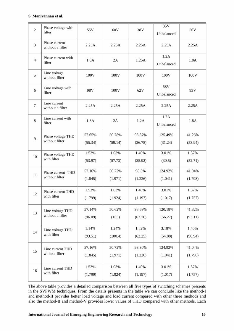
The simulation parameters used are; DC input voltage = 100V, fundamental frequency = 50Hz, ODE solver = ode45 (Dormand-Prince), switching frequency = 12 kHz, modulation index = 0.87, load type
= constant Z, load = star connected R-L load, active power = 1kW, inductive reactive power = 1000e-
3VAR, filter = second order filters. The performance of two level SVPWM modulated three phase VSI is analyzed by considering parameters. The comparative statements of each parameter are given
below.
Table-4. Comparative results statement of all five possible switching schemes
Sl.No Performance
Parameters Method-I Method-II Method-III Method-IV Method-V
1 Phase voltage
without filter 68V 68V 67.5V 67.5V 67V
S. Manivannan et al.
International Journal of Emerging Engineering Research and Technology 16
2 Phase voltage with
filter 55V 60V 38V
35V
Unbalanced 56V
3 Phase current
without a filter 2.25A 2.25A 2.25A 2.25A 2.25A
4 Phase current with
filter 1.8A 2A 1.25A
1.2A
Unbalanced 1.8A
5 Line voltage
without filter 100V 100V 100V 100V 100V
6 Line voltage with
filter 98V 100V 62V
58V
Unbalanced 93V
7 Line current
without a filter 2.25A 2.25A 2.25A 2.25A 2.25A
8 Line current with
filter 1.8A 2A 1.2A
1.2A
Unbalanced 1.8A
9 Phase voltage THD
without filter
57.65%
(55.34)
50.78%
(59.14)
98.87%
(36.78)
125.49%
(31.24)
41.26%
(53.94)
10 Phase voltage THD
with filter
1.52%
(53.97)
1.03%
(57.73)
1.40%
(35.92)
3.01%
(30.5)
1.37%
(52.71)
11 Phase current THD
without filter
57.16%
(1.845)
50.72%
(1.971)
98.3%
(1.226)
124.92%
(1.041)
41.04%
(1.798)
12 Phase current THD
with filter
1.52%
(1.799)
1.03%
(1.924)
1.40%
(1.197)
3.01%
(1.017)
1.37%
(1.757)
13 Line voltage THD
without a filter
57.14%
(96.09)
50.62%
(103)
98.69%
(63.76)
120.18%
(56.27)
41.82%
(93.11)
14 Line voltage THD
with filter
1.14%
(93.51)
1.24%
(100.4)
1.82%
(62.25)
3.18%
(54.88)
1.40%
(90.94)
15 Line current THD
without filter
57.16%
(1.845)
50.72%
(1.971)
98.30%
(1.226)
124.92%
(1.041)
41.04%
(1.798)
16 Line current THD
with filter
1.52%
(1.799)
1.03%
(1.924)
1.40%
(1.197)
3.01%
(1.017)
1.37%
(1.757)
The above table provides a detailed comparison between all five types of switching schemes presents in the SVPWM techniques. From the details presents in the table we can conclude like the method-I
and method-II provides better load voltage and load current compared with other three methods and
also the method-II and method-V provides lower values of THD compared with other methods. Each

A Comparative Study of Different Approaches Presents in Two Level Space Vector Pulse Width
Modulated Three Phase Voltage Source Invertes
International Journal of Emerging Engineering Research and Technology 17
method had unique features and characteristics that will be varying with respect to types and load parameters.
9. SVPWM TECHNIQUE FOR Z-SOURCE AND T-SOURCE INVERTERS
All the above section represents the basic concepts recording SVPWM, the various switching schemes in SVPWM and the performance of 2-level three phase voltage source inverter. The same concepts
can be represented in the Z - Source inverter (ZSI) and T-Source inverter (TSI) also. The procedure
for switching sequence in ZSI and TSI are same as three phase voltage source inverter except the introduction of a shoot though zero state in ZSI. The following subsequent paper should explain these
concepts in details.
10. CONCLUSION
The SVPWM technique can only be applied to a three-phase inverter and it increases the overall
system efficiency. The SVPWM is used for controlling the switching of the machine side converter.
Advantages of this method include a higher modulation index, lower switching losses, and less harmonic distortion compared to SPWM. SVPWM research has been widespread in recent years,
making it one of the most popular methods for three-phase inverters because it has a higher
fundamental voltage output than SPWM for the same DC bus voltage. The SVPWM is significantly
better than SPWM by approximately 15.5%. However, the SVPWM technique is complex in implementation, especially in the over-modulation region. SVPWM technique has become the most
popular and important PWM technique for three phases VSI for the control of AC induction. This
paper has provided a thorough review of the each technique with a special focus on the operation of SVPWM in all the five possible switching schemes. In this paper, Simulink models for all five
possible switching schemes has been developed and tested in the MATLAB/SIMULINK
environment. This paper discusses the advantages and drawbacks of each switching schemes and their simulation results are compared and analyzed by plotting the output harmonic spectra of various
output voltages and computing their total harmonic distortions (THD). As seen from the simulation
results the DC bus utilization will be variable for all the five possible switching schemes, but the THD
will be varied for every switching sequence. From the simulation results we can come to the conclusion like the methods-II and III switching schemes having less THD when compared to the
other two methods of switching schemes. In the future researches there are some possibilities are
available for implementing the same switching schemes in three phase ZSI and TSI. Definitely the performance of ZSI and TSI will be varied with respect to its different switching schemes.
REFERENCES
[1] J. Holtz, “Pulse Width Modulation – A Survey”, IEEE Transaction on Industrial Electronics., Vol. 39, no. 5, Dec. 1992, pp. 410-420.
[2] Granado, J., Harley, R.G., Giana, G, “Understanding and Designing a Space Vector Pulse-
Width-Modulator to Control a Three Phase Inverter”, Transaction Of the SAIEEE (1989),
Vol.80, Sept.1989, pp. 29-37.
[3] Holtz, J. (1994). “Pulse Width Modulation for Electronic Power Conversion”, Proceedings of the
IEEE, Vol.82, No.8, pp. 1194-1214.
[4] Holms, D.G. (1996). “The Significance of Zero Space Vector Placements for Carrier-Based
PWM Schemes”, IEEE Transactions on Industry Applications, Vol. 32, No. 5, pp. 1122-1129.
[5] Zhai, L. and Li, H. (2008) “Modeling and Simulation of SVPWM Control System of Induction
Motor in Electric Vehicle”, IEEE International Conferences on Automation and Logistics, pp. 2026-2030.
[6] Bose, B. K, 2002, “Modern Power Electronics and AC Drives”, Prentice Hall PTR, New Jersey.
[7] J. H. Seo, C. H. Choi, and D.S. Hyun, “A new simplified space-vector pwm method for three-level inverters,” IEEE Transaction on Power Electronics, vol. 16, no. 4, pp. 545-550, Jul. 2001.
[8] T. Bruckner and D. G. Holmes, “Optimal pulse-width modulation for three-level inverters,” IEEE Transaction on Power Electronics, vol. 1, no. 20, pp. 82-89, Jan. 2005.

S. Manivannan et al.
International Journal of Emerging Engineering Research and Technology 18
[9] O. Ogasawara, H. Akagi, and A. Nabae, “A Novel PWM Scheme of Voltage Source Inverters
Based on Space Vector Theory,” EPE Europ. Conference in Power Electronics and Applications, Aachen, 1989, pp-1197-1202.
[10] G. S. Buja and G. B. Indri, “ Optimal Pulse width Modulation for Feeding AC Motors”, IEEE
Transaction on Industrial Applications, Vol. IA-13, No. 1, Jan. /Feb. 1977, pp. 38-44.
[11] A. Nabae, S. Ogasawara and H. Akagi, “A Novel Control Scheme for PWM Controlled
Inverters”, IEEE Industrial Applications Society Annual Meeting, Toronto, 1985, pp. 473-478.
[12] M. Rajender reddy, T. Brahmananda reddy, D. Subba rayudu, “Simple and novel unified pulse
width modulation algorithm for voltage source inverters in the entire modulation range” Acta
Electrotechnica et Informatica, Vol. 13, No. 3, 2013, 48–55, DOI: 10.2478/aeei-2013-0040.
[13] JBV Subrahmanyam, Sankar, “Application of svpwm technique to three level voltage source
inverter” International Journal of Engineering and Technology Volume 1 No. 1, October, 2011.
[14] K. Mounika, B. Kiran Babu, “Sinusoidal and Space Vector Pulse Width Modulation for Inverter”
International Journal of Engineering Trends and Technology (IJETT) - Volume4Issue4- April 2013.
[15] S.Meenakshi Sundaravel and Dr.S.Murugan, “Modified Cascaded H-Bridge Multilevel Inverter
topology with Reduced Number of Power Electronic Switching Components” International
Journal of Electrical Engineering. ISSN 0974-2158 Volume 6, Number 2 (2013), pp. 137-149.
[16] K. Vinothkumar, “Simulation and Comparison of SPWM and SVPWM Control for Three Phase
Inverter”, ARPN Journal of Engineering and Applied Sciences, Vol. 5, No. 7, July-2010.
[17] D. G. Holmes and T. A. Lipo. 2003. “Pulse Width Modulation for Power Converters: Principles
and Practice”. New Jersey: IEEE Press, Wiley Publications, New York, USA.
[18] Bin Wu “High-Power Converters and AC Drives”, IEEE Press, Wiley-Interscience. pp. 95-117.
[19] Zhou, K., and Wang, D. “Relationship between space-vector modulation and three-phase carrier-
based PWM: A comprehensive analysis”, IEEE Trans. Industrial Electronics., 2002, 49-1, pp. 186-196.
[20] N. Mohan, T. R. Undeland, W. P. Robbins, “Power Electronic Converters, Applications, and Design”, John Wiley & Sons, Inc. Media Enhanced Third Edition.
[21] Phuong Hue Tran, “Matlab/Simulink implementation and analysis of three pulse-width-modulation (PWM) techniques”, Master of Science in Electrical Engineering, Boise State
University, May 2012.
[22] Jin-Woo Jung, “Space Vector PWM Inverter”, Ph.D., Thesis, Department of Electrical and
Computer Engineering, The Ohio State University, Feb.20, 2005.
[23] Muhammad H. Rashid, “Power Electronics Handbook”, Academic Press Series in Engineering.


![CHAPTER 3 PWM SCHEMES IN THREE PHASE ...technique known as Space Vector Modulation [3.2] is used which will be discussed in the following section. 3.4 Space Vector Modulation SVPWM](https://static.fdocuments.us/doc/165x107/5e8db9bb659c952bfd62b2a9/chapter-3-pwm-schemes-in-three-phase-technique-known-as-space-vector-modulation.jpg)