A CALL TO ADVANCING NANOTECHNOLOGY DEVELOPMENT IN CONNECTICUT · The Connecticut Office for...
101
A CALL T O A CTION: ADVANCING NANOTECHNOLOGY DEVELOPMENT IN CONNECTICUT PREPARED FOR: The Connecticut Office for Workforce Competitiveness PREPARED BY: Technology Partnership Practice Battelle Cleveland, Ohio May 2005 © 2005 Battelle Memorial Institute FINAL REPORT
Transcript of A CALL TO ADVANCING NANOTECHNOLOGY DEVELOPMENT IN CONNECTICUT · The Connecticut Office for...

A CALL TO ACTION:ADVANCING NANOTECHNOLOGYDEVELOPMENT IN CONNECTICUT
PREPARED FOR:The Connecticut Office for Workforce Competitiveness
PREPARED BY:Technology Partnership PracticeBattelle Cleveland, Ohio
May 2005
© 2
005
Bat
telle
Mem
oria
l Ins
titut
e
FINAL REPORT

Battelle Memorial Institute (Battelle) does not endorse or recommend particular companies, products, services, or technologies nor does it endorse or recommend financial investments and/or the purchase or sale of securities. Battelle makes no warranty or guarantee, express or implied, including without limitation, warranties of fitness for a particular purpose or merchantability, for any report, service, data or other information provided herein.
Copyright 2005 Battelle Memorial Institute. Use, duplication, or distribution of this document or any part thereof is prohibited without the written permission of Battelle Memorial Institute. Unauthorized use may
violate the copyright laws and result in civil and/or criminal penalties.
Table of Contents
Executive Summary ................................................................................................................................ ES-1 Introduction ............................................................................................................................................ 1
The Potential of Nanotechnology ............................................................................................................. 1 Focus of Strategic Assessment ................................................................................................................. 1 Study Approach ........................................................................................................................................ 2
Section I. Setting the Context for Understanding Nanotechnology Development ...................................... 5 The Stakes for Connecticut in Nanotechnology are High ........................................................................ 6
Other Impacts of Nanotechnology ....................................................................................................... 7 Nanotechnology Faces Commercialization Challenges ........................................................................... 9 The National Nanotechnology Initiative Is an Asset, But Not a Program............................................. 11 Other States are Taking the Lead in Nanotechnology Development...................................................... 14
Section II. Analysis of Connecticut’s University and Industry Nanotechnology Activities...................... 17 Connecticut’s Current Position............................................................................................................... 17
University Research Position ............................................................................................................. 17 Industry and University Patent Activity............................................................................................. 18 Industry Research and Development Activity.................................................................................... 21 Industry–University Collaboration..................................................................................................... 21
Summary of Connecticut’s Strategic Position: SWOT Analysis............................................................ 21 Strengths .......................................................................................................................................... 22 Weaknesses ........................................................................................................................................ 22 Opportunities...................................................................................................................................... 22 Threats .......................................................................................................................................... 22
Section III. Strategic Framework for Connecticut in Nanotechnology Development ............................... 23 A Situational Assessment ....................................................................................................................... 23 Vision and Mission for Connecticut in Nanotechnology........................................................................ 24 Proposed Five-Year Action Plan to Move Connecticut Forward ........................................................... 25
Seven Priority Actions ....................................................................................................................... 25 Approaches to Implementing the Proposed Action Steps .................................................................. 27
Endnotes .......................................................................................................................................... 29 Appendix A. Connecticut Companies Actively Engaged in Nanotechnology R&D and/or Product Development, by Value Chain Segment ..................................................................................................... 31 Appendix B. Federal Agency Approaches as Part of the National Nanotechnology Initiative .................. 33 Appendix C. Benchmarking Case Studies and Best Practice Lessons....................................................... 55 Appendix D. Key Nanotechnology Research Themes within the University of Connecticut and Yale University, by Value Chain and Key Sectors ............................................................................................. 87


ES-1
Figure ES-1. Project Plan for Developing the Connecticut Nanotechnology Strategic Framework
Executive Summary
INTRODUCTION Nanotechnology, the understanding and control of matter at dimensions of roughly one to 100 nanometers, is an emerging field of technology viewed by many as leading the next industrial revolution. Indeed, recent progress in the measurement, modeling, and manipulation of matter at the nanoscale has mankind on the verge of revolutionizing materials, data storage and processing, sensors, power generation, environment, and medicine.
For Connecticut, nanotechnology has significant implications for the state’s overall economic competitiveness. A recent study for the Connecticut Office for Workforce Competitiveness, Connecticut’s Core Competencies for the Knowledge Economy, reveals that Connecticut has strategic technology opportunity areas, drawing upon its broad range of core competencies, that can be affected by nanotechnology, involving advanced product development, biomedical engineering, and translational medicine.
Even more compelling is that nanotechnology can be seen as an opportunity to build upon (a) the natural evolution of Connecticut’s long-standing, specialized, and distinctive capabilities to reach ever-diminishing scales of production (“top-down” nanotechnology development); and (b) the state’s scientific and engineering talent to pursue new materials, coatings, catalysts, and other applications at the atomic scale (“bottom-up” nanotechnology development).
Given the emerging nature of nanotechnology, much of this field is at the stage of fundamental research and testing performed by university researchers and, to a lesser extent, corporate research and development (R&D) laboratories. To develop Connecticut’s potential in nanotechnology, it is critical for the state to understand the current position of its universities and industry with regards to research performance and funding, the generation of intellectual property, and the collaboration of industry and university, as well as which specific sectors of Connecticut’s technology-rich industrial base are mastering and advancing nanotechnology skill sets and which are failing to do so.
Focus of Strategic Assessment
This report provides a comprehensive examination of the significance to and relative position of Connecticut in nanotechnology. Based on this comprehensive review and analysis, the report lays out a strategic framework for Connecticut to guide future investments and activities in nanotechnology as shown in Figure ES-1.
Development of Strategic
Framework Vision
Gaps, Situational Analysis,
Opportunities,Strategies,
Actions
Gap Analysis & SWOT Review
Assessment of Connecticut’s Industry and
University Position in
Nanotechnology
Layman’s Guide to Nanotech
Challenges to Commercial-
ization
Setting the Context Strategic Assessment Strategic Framework
Overview of National
Nanotech Initiative
Best Practices
from Leading States
ES-2
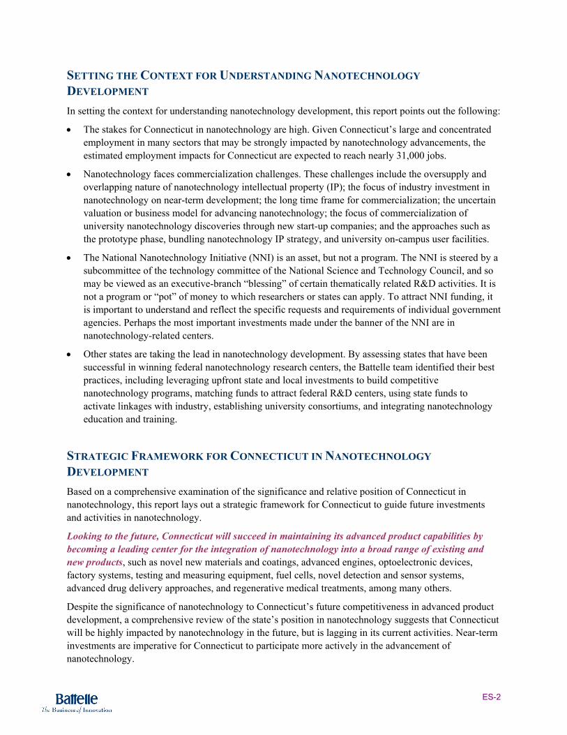
SETTING THE CONTEXT FOR UNDERSTANDING NANOTECHNOLOGY DEVELOPMENT In setting the context for understanding nanotechnology development, this report points out the following:
• The stakes for Connecticut in nanotechnology are high. Given Connecticut’s large and concentrated employment in many sectors that may be strongly impacted by nanotechnology advancements, the estimated employment impacts for Connecticut are expected to reach nearly 31,000 jobs.
• Nanotechnology faces commercialization challenges. These challenges include the oversupply and overlapping nature of nanotechnology intellectual property (IP); the focus of industry investment in nanotechnology on near-term development; the long time frame for commercialization; the uncertain valuation or business model for advancing nanotechnology; the focus of commercialization of university nanotechnology discoveries through new start-up companies; and the approaches such as the prototype phase, bundling nanotechnology IP strategy, and university on-campus user facilities.
• The National Nanotechnology Initiative (NNI) is an asset, but not a program. The NNI is steered by a subcommittee of the technology committee of the National Science and Technology Council, and so may be viewed as an executive-branch “blessing” of certain thematically related R&D activities. It is not a program or “pot” of money to which researchers or states can apply. To attract NNI funding, it is important to understand and reflect the specific requests and requirements of individual government agencies. Perhaps the most important investments made under the banner of the NNI are in nanotechnology-related centers.
• Other states are taking the lead in nanotechnology development. By assessing states that have been successful in winning federal nanotechnology research centers, the Battelle team identified their best practices, including leveraging upfront state and local investments to build competitive nanotechnology programs, matching funds to attract federal R&D centers, using state funds to activate linkages with industry, establishing university consortiums, and integrating nanotechnology education and training.
STRATEGIC FRAMEWORK FOR CONNECTICUT IN NANOTECHNOLOGY DEVELOPMENT Based on a comprehensive examination of the significance and relative position of Connecticut in nanotechnology, this report lays out a strategic framework for Connecticut to guide future investments and activities in nanotechnology.
Looking to the future, Connecticut will succeed in maintaining its advanced product capabilities by becoming a leading center for the integration of nanotechnology into a broad range of existing and new products, such as novel new materials and coatings, advanced engines, optoelectronic devices, factory systems, testing and measuring equipment, fuel cells, novel detection and sensor systems, advanced drug delivery approaches, and regenerative medical treatments, among many others.
Despite the significance of nanotechnology to Connecticut’s future competitiveness in advanced product development, a comprehensive review of the state’s position in nanotechnology suggests that Connecticut will be highly impacted by nanotechnology in the future, but is lagging in its current activities. Near-term investments are imperative for Connecticut to participate more actively in the advancement of nanotechnology.
ES-3
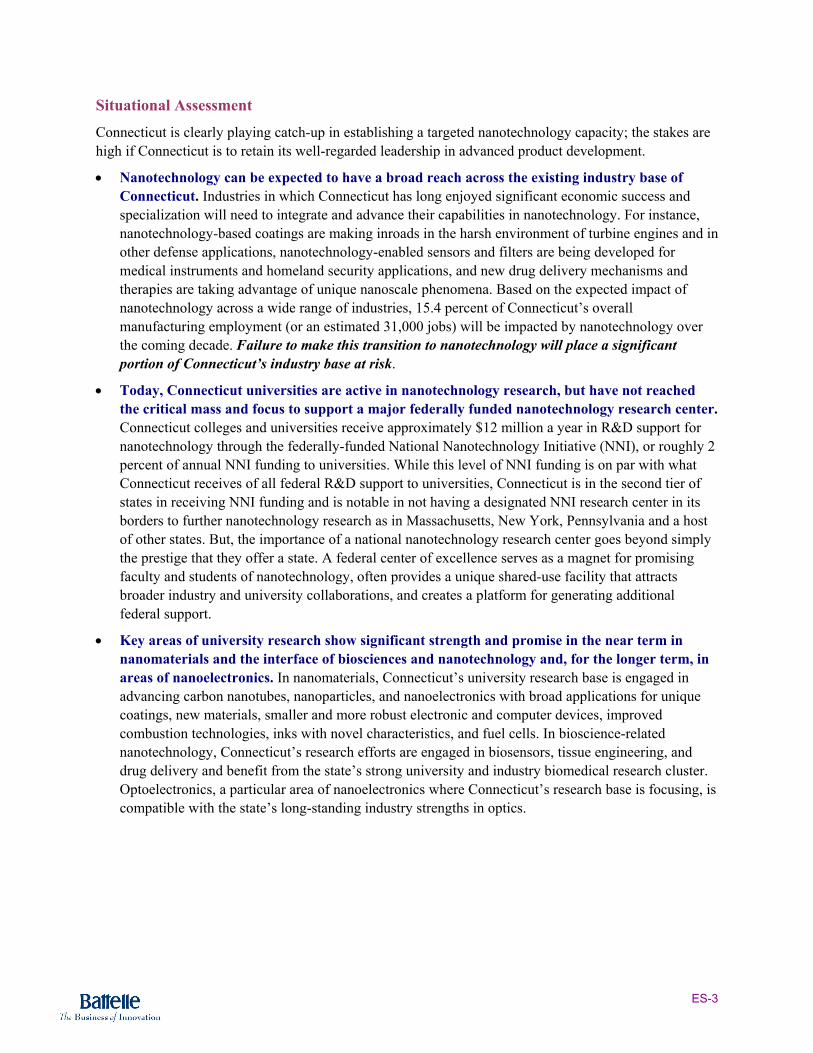
Situational Assessment
Connecticut is clearly playing catch-up in establishing a targeted nanotechnology capacity; the stakes are high if Connecticut is to retain its well-regarded leadership in advanced product development.
• Nanotechnology can be expected to have a broad reach across the existing industry base of Connecticut. Industries in which Connecticut has long enjoyed significant economic success and specialization will need to integrate and advance their capabilities in nanotechnology. For instance, nanotechnology-based coatings are making inroads in the harsh environment of turbine engines and in other defense applications, nanotechnology-enabled sensors and filters are being developed for medical instruments and homeland security applications, and new drug delivery mechanisms and therapies are taking advantage of unique nanoscale phenomena. Based on the expected impact of nanotechnology across a wide range of industries, 15.4 percent of Connecticut’s overall manufacturing employment (or an estimated 31,000 jobs) will be impacted by nanotechnology over the coming decade. Failure to make this transition to nanotechnology will place a significant portion of Connecticut’s industry base at risk.
• Today, Connecticut universities are active in nanotechnology research, but have not reached the critical mass and focus to support a major federally funded nanotechnology research center. Connecticut colleges and universities receive approximately $12 million a year in R&D support for nanotechnology through the federally-funded National Nanotechnology Initiative (NNI), or roughly 2 percent of annual NNI funding to universities. While this level of NNI funding is on par with what Connecticut receives of all federal R&D support to universities, Connecticut is in the second tier of states in receiving NNI funding and is notable in not having a designated NNI research center in its borders to further nanotechnology research as in Massachusetts, New York, Pennsylvania and a host of other states. But, the importance of a national nanotechnology research center goes beyond simply the prestige that they offer a state. A federal center of excellence serves as a magnet for promising faculty and students of nanotechnology, often provides a unique shared-use facility that attracts broader industry and university collaborations, and creates a platform for generating additional federal support.
• Key areas of university research show significant strength and promise in the near term in nanomaterials and the interface of biosciences and nanotechnology and, for the longer term, in areas of nanoelectronics. In nanomaterials, Connecticut’s university research base is engaged in advancing carbon nanotubes, nanoparticles, and nanoelectronics with broad applications for unique coatings, new materials, smaller and more robust electronic and computer devices, improved combustion technologies, inks with novel characteristics, and fuel cells. In bioscience-related nanotechnology, Connecticut’s research efforts are engaged in biosensors, tissue engineering, and drug delivery and benefit from the state’s strong university and industry biomedical research cluster. Optoelectronics, a particular area of nanoelectronics where Connecticut’s research base is focusing, is compatible with the state’s long-standing industry strengths in optics.

ES-4
• Connecticut is not a “hot spot” of industry nanotechnology activity. On a positive note, this study identifies over two dozen companies in Connecticut where nanotechnology and nanoscale phenomena currently impact the research, development, products, and near-term business functions and opportunities. Yet, for the most part, the remaining Connecticut companies are not actively engaged in nanotechnology activities. Moreover, many Connecticut companies engaged in nanotechnology are actually conducting this work in their out-of-state research laboratories or with key partners outside of Connecticut. Finally, the vast majority of Connecticut companies needing to integrate nanotechnologies as they advance are acting as spectators rather than participants. The key question is whether Connecticut companies will be able to gain the skill sets and knowledge of advancing nanotechnology and whether that activity will take place in Connecticut.
• Connecticut is being outflanked by other states because it lacks an investment program. Other states have actively targeted investments to establish a focus of nanotechnology research that can enable their universities to build the capacity to attract federal nanotechnology research centers. These states often directly invest matching funds to win these federal research centers. Connecticut is largely absent in its investments in nanotechnology, and even areas of funding that have the potential to advance nanotechnology—such as the Clean Energy Fund—are not being tapped.
Summary of Connecticut’s Strengths, Weaknesses, Opportunities, and Threats in Nanotechnology Strengths
• Growing base of university research with emphasis on several areas of nanotechnology research
• Strong Small Business Innovation Research (SBIR) grant activity of Connecticut companies
• Presence of over two dozen companies in Connecticut focused on nanotechnology development
Weaknesses
• No national nanotechnology centers of excellence in Connecticut
• Not a national leader in university or industry nanotechnology-R&D activity as measured by grant and patent activity
• Few large companies engaged in conducting nanotechnology R&D work in-state
• Limited industry-university interactions in nanotechnology R&D
• No significant nanotechnology tools development stemming from Connecticut’s machinery/ instruments legacy
• Significant gaps in technology infrastructure
Opportunities
• Strong advanced product development industry complex in Connecticut, needing to integrate nanotechnology in the future to remain competitive
• University and industry strengths in the biosciences in Connecticut, opening opportunities for advancing bioscience-nanotechnology applications
• Proximity to nearby universities and national labs with centers of excellence in nanotechnology research
• Pursuit of commonalities between industry needs and university research in materials, coatings, membranes, filters, and sensors for biomedical, energy, and homeland security applications
Threats
• Lack of focused state support, making Connecticut less competitive with other states
• Major federal nanotechnology infrastructure investment window coming to a close—difficult to attract a research center to Connecticut with more than 40 centers currently funded
• Federal budget constraints—already expected to impact Department of Defense research funding
• Companies advancing nanotechnology-related product developments out-of-state
ES-5
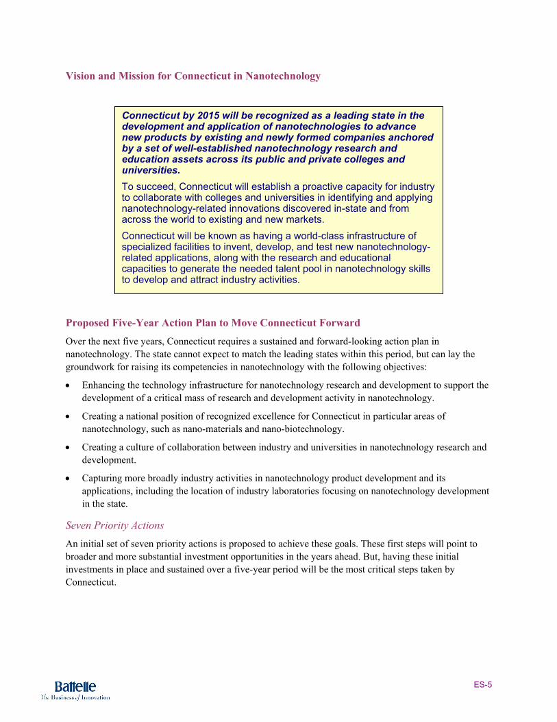
Vision and Mission for Connecticut in Nanotechnology
Proposed Five-Year Action Plan to Move Connecticut Forward
Over the next five years, Connecticut requires a sustained and forward-looking action plan in nanotechnology. The state cannot expect to match the leading states within this period, but can lay the groundwork for raising its competencies in nanotechnology with the following objectives:
• Enhancing the technology infrastructure for nanotechnology research and development to support the development of a critical mass of research and development activity in nanotechnology.
• Creating a national position of recognized excellence for Connecticut in particular areas of nanotechnology, such as nano-materials and nano-biotechnology.
• Creating a culture of collaboration between industry and universities in nanotechnology research and development.
• Capturing more broadly industry activities in nanotechnology product development and its applications, including the location of industry laboratories focusing on nanotechnology development in the state.
Seven Priority Actions
An initial set of seven priority actions is proposed to achieve these goals. These first steps will point to broader and more substantial investment opportunities in the years ahead. But, having these initial investments in place and sustained over a five-year period will be the most critical steps taken by Connecticut.
Connecticut by 2015 will be recognized as a leading state in the development and application of nanotechnologies to advance new products by existing and newly formed companies anchored by a set of well-established nanotechnology research and education assets across its public and private colleges and universities. To succeed, Connecticut will establish a proactive capacity for industry to collaborate with colleges and universities in identifying and applying nanotechnology-related innovations discovered in-state and from across the world to existing and new markets. Connecticut will be known as having a world-class infrastructure of specialized facilities to invent, develop, and test new nanotechnology-related applications, along with the research and educational capacities to generate the needed talent pool in nanotechnology skills to develop and attract industry activities.

ES-6
Figure ES-2. Integrative and Reinforcing Aspects of Proposed Nanotechnology Action Steps for Connecticut
The seven initial priority actions are as follows:
1. Establish a state-of-the-art Connecticut Nanotechnology Characterization Facility in a central location to serve Connecticut’s public and private colleges and universities and industry from across the state.
2. Retain and recruit entrepreneurial Eminent Scholars in nanotechnology across colleges and universities in Connecticut.
3. Provide seed grants targeted to nanotechnology for multi-institutional research collaborations and industry R&D partnerships with colleges and universities.
4. Develop a Strategic Matching Fund of $15 million to $25 million for future applications for federally funded nanotechnology research centers or major industry nanotechnology laboratories.
5. Establish a Technical Nanotechnology Forum that can be a peer-to-peer network for scientists and engineers involved in nanotechnology R&D in the state across the broad base of higher education and industry.
6. Create a Nanotechnology Education Clearinghouse to sponsor curriculum development, support professional development of teachers, and encourage access to specialized instructional laboratories.
7. Establish a proof-of-concept funding to advance nanotechnology discoveries and validate their potential for commercialization, with active linkage to pursuing federal SBIR funds.
Individually, each action is an important step to strengthen Connecticut’s competitive position in nanotechnology. But together, they can form a highly integrated and reinforcing approach in which each action serves as a resource or a generator of demand for the other actions, as suggested in Figure ES-2.
Seed Grants for Industry-University Collaborations
Strategic Matching Fundfor Federal Centers
Technical Nanotech Forum
Nano-CharacterizationFacility
Educational Clearinghouse
Proof-of-ConceptFunding
Entrepreneurial, EminentScholars
Key
Reso
urce
Key Resource
Key R
esour
ce Key Resource
Key Attraction to Recruit
Provide Industry Involvement
Source of IdeasSource of Opportunities
Source of Resources and Ideas
Source of Ideas Source of Ideas
Leading Contributors
Leading Contributors
Source of Ideas

ES-7
Approaches to Implementing the Proposed Action Steps
If implemented as a dedicated nanotechnology initiative, these seven action steps can serve as the backbone of a more focused “technology accelerator” in nanotechnology for Connecticut. The concept of a technology accelerator was envisioned by the Connecticut Technology Transfer and Commercialization Advisory Board of the Governor’s Competitiveness Council as “a focal point to coordinate various R&D, technology transfer and entrepreneurial activities in the state” for defined areas of core competencies.
Alternatively, these seven action steps can be pursued more independently because many can be incorporated into either ongoing initiatives or broader initiatives supporting more than nanotechnology. For instance, nanotechnology can be just one of several technology targets for recruiting entrepreneurial Eminent Scholars to Connecticut or for proof-of-concept funding.
Once the choice of approach is determined, a full-scale prospectus or operating plan can be completed, involving more detailed implementation plans such as specifics on the design, resource requirements, lead organizations, and milestones to be achieved.

ES-8

1
Introduction
THE POTENTIAL OF NANOTECHNOLOGY Nanotechnology is viewed by many as leading the next industrial revolution. Indeed, recent progress in the measurement, modeling, and manipulation of matter at the nanoscale has mankind on the verge of revolutionizing materials, data storage and processing, sensors, power generation, environment, and medicine. An interagency working group of the National Science and Technology Council (NSTC) characterized nanotechnology as having “the potential to change the nature of almost every human-made object, because control at the nanoscale means tailoring the fundamental properties, phenomena, and processes exactly at the scale where electronic, chemical, and biological properties and phenomena are defined.”1 Furthermore, the National Nanotechnology Initiative (NNI)—the federal government’s effort to coordinate and direct nanotechnology research and development (R&D) activities resulting from these NSTC efforts—forecasts as follows: “The impact of nanotechnology on the health, wealth, and lives of people could be at least as significant as the combined influences of microelectronics, medical imaging, computer-aided engineering, and man-made polymers developed in this century.”2
Given this potentially broad impact of nanotechnology, it is important for Connecticut to consider how it is positioned to participate in this new wave of technology advancement. In particular, it is critical for the state to learn which specific sectors of Connecticut’s technology-rich industrial base are mastering and advancing nanotechnology skill sets and which are failing to do so. Moreover, collaborations with universities are key in nanotechnology because so much of this field is at the stage of fundamental research and testing and is supported by significant federal funding to universities. Therefore, Connecticut needs to consider how its universities are positioned for advancing nanotechnology sciences and techniques.
FOCUS OF STRATEGIC ASSESSMENT The Connecticut Office for Workforce Competitiveness, as part of its recent statutory charge to advance Knowledge Economy policies for the state, has commissioned this study to assess Connecticut’s relative position in nanotechnology and develop a strategic approach to advance the state’s nanotechnology resources and assets.
What is Nanotechnology?
Nanotechnology is the understanding and control of matter at dimensions of roughly one to 100 nanometers, where unique phenomena enable novel applications. A nanometer is one-billionth of a meter; a sheet of paper is about 100,000 nanometers thick. Encompassing nanoscale science, engineering, and technology, nanotechnology involves imaging, measuring, modeling, and manipulating matter at this length scale. At this level, the physical, chemical, and biological properties of materials differ in fundamental and valuable ways from the properties of individual atoms and molecules or bulk matter. Nanotechnology R&D is directed toward understanding and creating improved materials, devices, and systems that exploit these new properties. The National Nanotechnology Initiative Strategic Plan, December 2004
2
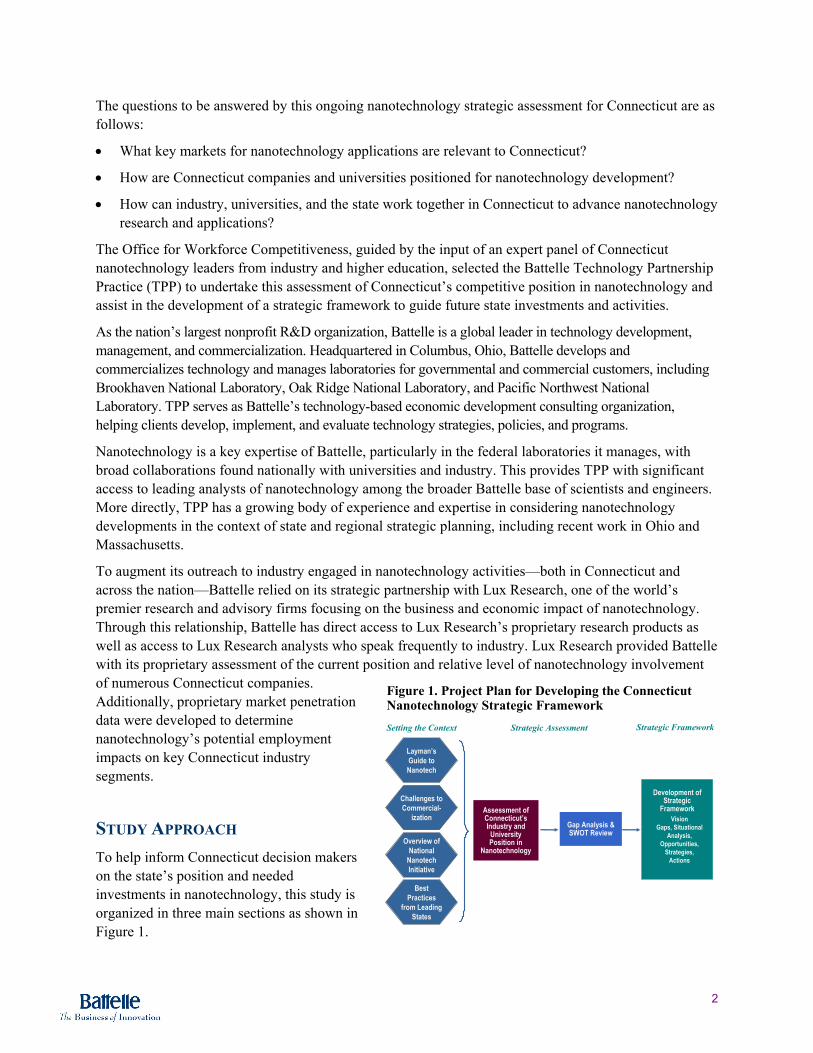
The questions to be answered by this ongoing nanotechnology strategic assessment for Connecticut are as follows:
• What key markets for nanotechnology applications are relevant to Connecticut?
• How are Connecticut companies and universities positioned for nanotechnology development?
• How can industry, universities, and the state work together in Connecticut to advance nanotechnology research and applications?
The Office for Workforce Competitiveness, guided by the input of an expert panel of Connecticut nanotechnology leaders from industry and higher education, selected the Battelle Technology Partnership Practice (TPP) to undertake this assessment of Connecticut’s competitive position in nanotechnology and assist in the development of a strategic framework to guide future state investments and activities.
As the nation’s largest nonprofit R&D organization, Battelle is a global leader in technology development, management, and commercialization. Headquartered in Columbus, Ohio, Battelle develops and commercializes technology and manages laboratories for governmental and commercial customers, including Brookhaven National Laboratory, Oak Ridge National Laboratory, and Pacific Northwest National Laboratory. TPP serves as Battelle’s technology-based economic development consulting organization, helping clients develop, implement, and evaluate technology strategies, policies, and programs.
Nanotechnology is a key expertise of Battelle, particularly in the federal laboratories it manages, with broad collaborations found nationally with universities and industry. This provides TPP with significant access to leading analysts of nanotechnology among the broader Battelle base of scientists and engineers. More directly, TPP has a growing body of experience and expertise in considering nanotechnology developments in the context of state and regional strategic planning, including recent work in Ohio and Massachusetts.
To augment its outreach to industry engaged in nanotechnology activities—both in Connecticut and across the nation—Battelle relied on its strategic partnership with Lux Research, one of the world’s premier research and advisory firms focusing on the business and economic impact of nanotechnology. Through this relationship, Battelle has direct access to Lux Research’s proprietary research products as well as access to Lux Research analysts who speak frequently to industry. Lux Research provided Battelle with its proprietary assessment of the current position and relative level of nanotechnology involvement of numerous Connecticut companies. Additionally, proprietary market penetration data were developed to determine nanotechnology’s potential employment impacts on key Connecticut industry segments.
STUDY APPROACH To help inform Connecticut decision makers on the state’s position and needed investments in nanotechnology, this study is organized in three main sections as shown in Figure 1.
Development of Strategic
Framework Vision
Gaps, Situational Analysis,
Opportunities,Strategies,
Actions
Gap Analysis & SWOT Review
Assessment of Connecticut’s Industry and
University Position in
Nanotechnology
Layman’s Guide to Nanotech
Challenges to Commercial-
ization
Setting the Context Strategic Assessment Strategic Framework
Overview of National
Nanotech Initiative
Best Practices
from Leading States
Figure 1. Project Plan for Developing the Connecticut Nanotechnology Strategic Framework

3
Section I sets the context to assist Connecticut decision makers and the public at large in understanding the importance of nanotechnology and the development challenges it is expected to face. This includes explaining
• The importance of nanotechnology within the context of Connecticut’s economy and how it might impact the state in the future;
• The focus of key drivers of nanotechnology and the challenges to realizing nanotechnology’s commercial potential; and
• The benchmarking of activities of leading states in nanotechnology to learn more about the approaches being pursued by states to develop nanotechnology.
Section II assesses Connecticut’s competitive position in nanotechnology. It examines the level and focus of nanotechnology activities found across Connecticut’s university and industry players and evaluates Connecticut’s relative standing in key indicators, such as patent and federal grant activities. Section II results in a more strategic view of Connecticut, identifying the state’s strengths, weaknesses, opportunities, and threats in nanotechnology development.
Section III sets out a strategic framework to guide Connecticut’s future actions to develop nanotechnology in the state. This section puts forth a vision, strategic priorities, and key actions necessary to support those strategies.

4

5
The Value of Nanotechnology
Nanotechnology is not a market or an industry; instead, it is an essential enabler that will impact all manufactured goods. Nanotechnology will account for $158 billion in product revenue this year, but 92 percent of it will derive from established materials and processes that happen to have nanoscale dimensions as opposed to new, emerging innovations. In the next ten years, revenue will grow 18 times over and the balance [between established and emerging nanotechnology] will flip: In 2014 nanotechnology will be incorporated in products worth $2.9 trillion in revenue, with new, emerging nanotechnology accounting for 89 percent. Revenues of products incorporating nanotechnology will exceed biotechnology by ten times and have an economic impact on par with information technology and telecom. “Sizing Nanotechnology’s Value Chain,” Lux Research, Inc., 2004
Section I. Setting the Context for Understanding Nanotechnology Development
Nanotechnology is not only disruptive—manipulating matter and creating fundamentally new properties and functions for materials and devices—it is an enabling technology expected to span nearly every market and industry sector involved in goods production. Lux Research—one of the leading analysts of nanotechnology development—explains as follows:
Manufacturing, electronics, and pharmaceutical firms all stand to benefit from similar nanoscale innovations. But these companies have little to do with one another and will exploit the same basic advances in radically different ways. These unrelated corporations don’t constitute some mythical, cohesive “nanotechnology market”—instead, they each incorporate nanotechnology into their industry value chains…3
Nanotechnology is not unique in possessing this enabling quality. Electronics and information technology have similar enabling aspects, reaching across markets and industries not only to improve existing products, but offer new ways of doing business. Nanotechnology will not only affect “producers” of products but “users” as well—much the same as information technology and advanced communications.
To set the context for understanding the importance of nanotechnology and the development challenges it is expected to face, this section explains the following:
• The expected role of nanotechnology among Connecticut’s leading industry sectors
• The challenges arising to realizing nanotechnology’s commercial potential
• The role of the federal NNI
• The best practices of states leading in nanotechnology development.

6
THE STAKES FOR CONNECTICUT IN NANOTECHNOLOGY ARE HIGH For Connecticut, nanotechnology has significant implications for the state’s overall economic competitiveness. A recent study for the Office for Workforce Competitiveness, Connecticut’s Core Competencies for the Knowledge Economy, reveals that Connecticut has strategic technology opportunity areas, drawing upon its broad range of core competencies, that can be affected by nanotechnology, involving advanced product development, biomedical engineering, and translational medicine.4
Even more compelling is that nanotechnology can be seen as an opportunity to build upon (a) the natural evolution of Connecticut’s long-standing, specialized, and distinctive capabilities to reach ever-diminishing scales of production (“top-down” nanotechnology development); and (b) the state’s scientific and engineering talent to pursue new materials, coatings, catalysts, and other applications at the atomic scale (“bottom-up” nanotechnology development).
Employment and Revenue Impacts of Nanotechnology for Connecticut
This study identifies over two dozen companies in Connecticut where nanotechnology and nanoscale phenomena currently impact the R&D, intellectual property, products, and near-term business functions and opportunities (see Appendix A for a list of these Connecticut companies by Value Chain Segment). Given the state’s size and the emerging nature of nanotechnology, these firms represent a fairly robust base upon which to build:
• Most of these companies are in a broadly defined nanomaterial and related applications areas (e.g., coatings, materials, chemicals, inks, catalysts) or specific products that utilize nanomaterials.
• A few are pursuing nanotechnology-enabled devices or technologies either in electronics/semiconductor-related areas or in the bio-assay/nanofluidics area.
• Additionally, a substantial number of Connecticut firms are currently examining the role and potential that nanotechnology could play in the future of their businesses.
As an enabling technology, nanotechnology has and will have the ability to greatly impact manufacturing employment. Lux Research estimates that nanotechnology-enabled applications and products could account for $2.9 trillion revenue by 2014. Using the standard metric of $250,000 in sales per employee, nanotechnology impacted workers should account for slightly more than 12.5 percent of all U.S. manufacturing employment by 2014.
However, exactly how and when industries adopt and implement nanotechnology-based solutions and create nanotechnology-enabled applications and products can vary significantly by industry and value chain, resulting in differing employment impacts. These workers will be employed throughout the nanotechnology value chain, including key Connecticut industries such as materials, coatings, instruments, aerospace, machinery, and pharmaceuticals.
Using Lux Research’s proprietary nanotechnology penetration and implementation forecast data, the Battelle team developed for Connecticut’s key industries (key in terms of employment, regional concentration, or both) estimates of the potential employment impact by industry segment.5 Given Connecticut’s large and concentrated employment in many sectors that are forecast to be strongly impacted by nanotechnology advancements, the overall share of Connecticut manufacturing employment impacted by nanotechnology increases to 15.4 percent of the manufacturing base (2.9 percent greater than U.S. average), or an estimated 31,000 Connecticut jobs will be impacted by nanotechnology over the

7
coming decade.6 These jobs are a combination of jobs retained by Connecticut firms that, through the implementation of nanotechnology-enabled solutions, maintain or expand their competitiveness and new jobs in both existing and new firms that are developing new nanotechnology-base solutions to serve new market opportunities.
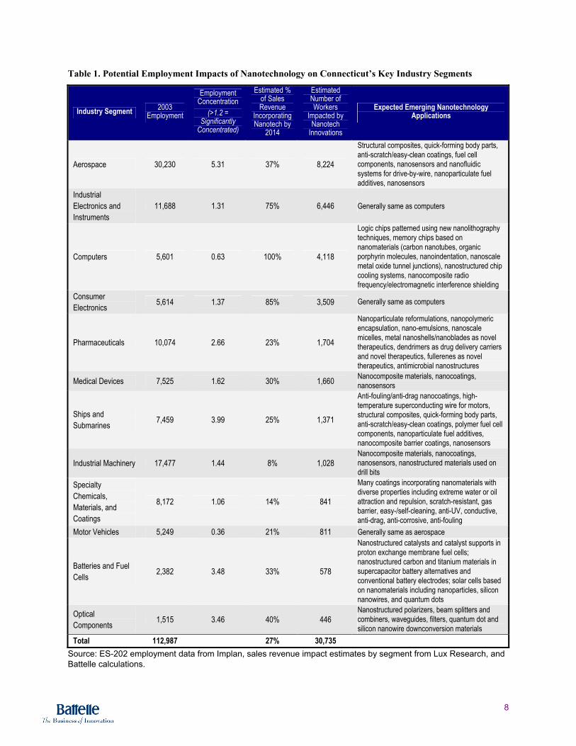
As shown in Table 1, the aerospace industry—the largest and most concentrated industry in Connecticut—will likely see more than one-third of its employment impacted by nanotechnology developments over the next decade, not including the additional impact on computers and electronics.
Industrial machinery, the state’s second largest industry, has a limited potential impact from nanotechnology according to Lux Research’s revenue impact forecasts. Yet, this situation could improve for Connecticut firms as newer, production-level industrial machinery is developed.
It is also important to note that the specialty chemicals, materials, and coatings industry has an expected revenue impact of 14 percent, leading to an employment impact of just under 850 jobs. However, given the existing nanotechnology involvement of Connecticut companies such as Inframat, the impact within the state could exceed this number.7
Other Impacts of Nanotechnology
Beyond potential revenue and employment impacts, nanotechnology can be expected to do the following:8
• “Simplify” supply chains—hurting many subassembly, metal machining, and other supply chain companies. By making basic materials more functional, nanotechnology will eliminate steps in manufacturing processes.
• Alter cost structures for manufacturing. As nanotechnology advances new manufacturing technologies—such as roll-to-roll display printing technologies for flat-panel display plants—it will create new approaches to manufacturing, possibly enabling unconventional competitors to enter established markets.
• Have many downstream effects on replacement and services related to manufactured goods. As nanotechnology creates longer-lasting products or self-healing materials, leading service repair and after-product markets will shrink.
8
Table 1. Potential Employment Impacts of Nanotechnology on Connecticut’s Key Industry Segments
Industry Segment 2003 Employment
Employment Concentration
(>1.2 = Significantly
Concentrated)
Estimated % of Sales Revenue
Incorporating Nanotech by
2014
Estimated Number of Workers
Impacted by Nanotech
Innovations
Expected Emerging Nanotechnology Applications
Aerospace 30,230 5.31 37% 8,224
Structural composites, quick-forming body parts, anti-scratch/easy-clean coatings, fuel cell components, nanosensors and nanofluidic systems for drive-by-wire, nanoparticulate fuel additives, nanosensors
Industrial Electronics and Instruments
11,688 1.31 75% 6,446 Generally same as computers
Computers 5,601 0.63 100% 4,118
Logic chips patterned using new nanolithography techniques, memory chips based on nanomaterials (carbon nanotubes, organic porphyrin molecules, nanoindentation, nanoscale metal oxide tunnel junctions), nanostructured chip cooling systems, nanocomposite radio frequency/electromagnetic interference shielding
Consumer Electronics 5,614 1.37 85% 3,509 Generally same as computers
Pharmaceuticals 10,074 2.66 23% 1,704
Nanoparticulate reformulations, nanopolymeric encapsulation, nano-emulsions, nanoscale micelles, metal nanoshells/nanoblades as novel therapeutics, dendrimers as drug delivery carriers and novel therapeutics, fullerenes as novel therapeutics, antimicrobial nanostructures
Medical Devices 7,525 1.62 30% 1,660 Nanocomposite materials, nanocoatings, nanosensors
Ships and Submarines 7,459 3.99 25% 1,371
Anti-fouling/anti-drag nanocoatings, high-temperature superconducting wire for motors, structural composites, quick-forming body parts, anti-scratch/easy-clean coatings, polymer fuel cell components, nanoparticulate fuel additives, nanocomposite barrier coatings, nanosensors
Industrial Machinery 17,477 1.44 8% 1,028 Nanocomposite materials, nanocoatings, nanosensors, nanostructured materials used on drill bits
Specialty Chemicals, Materials, and Coatings
8,172 1.06 14% 841
Many coatings incorporating nanomaterials with diverse properties including extreme water or oil attraction and repulsion, scratch-resistant, gas barrier, easy-/self-cleaning, anti-UV, conductive, anti-drag, anti-corrosive, anti-fouling
Motor Vehicles 5,249 0.36 21% 811 Generally same as aerospace
Batteries and Fuel Cells 2,382 3.48 33% 578
Nanostructured catalysts and catalyst supports in proton exchange membrane fuel cells; nanostructured carbon and titanium materials in supercapacitor battery alternatives and conventional battery electrodes; solar cells based on nanomaterials including nanoparticles, silicon nanowires, and quantum dots
Optical Components 1,515 3.46 40% 446
Nanostructured polarizers, beam splitters and combiners, waveguides, filters, quantum dot and silicon nanowire downconversion materials
Total 112,987 27% 30,735 Source: ES-202 employment data from Implan, sales revenue impact estimates by segment from Lux Research, and Battelle calculations.

9
NANOTECHNOLOGY FACES COMMERCIALIZATION CHALLENGES The road to commercializing nanotechnology is far from a smooth, functioning pipeline from discoveries to product development to market introduction, but one littered with significant pot holes and diversions.
One issue confronting nanotechnology is the oversupply and overlapping nature of nanotechnology intellectual property (IP). A technology transfer official at one of the nation’s leading nanotechnology universities explained to the Battelle project team that “patents are being filed with very broad claims and patents are starting to intersect…you are getting significant issues of freedom to operate and eventually either there will be lawsuits or parties will learn to play nice together.” Lux Research recently reviewed more than 1,000 patents issued for nanomaterials and has concluded as follows:
• The number of nanoscale inventions patented continues to rise at an accelerating rate. Anecdotal examples reveal some extremely broad claims, as well as claims that appear to overlap directly.
• Today’s state of affairs results from gold-rush thinking, confusing semantics, nanotechnology’s cross-disciplinary nature, and a stretched United States Patents and Trademarks Office.
• Companies are preparing to do battle over nanotechnology patents.
The IP muddle can halt venture capital investments in new start-up companies—since IP defines so much of the start-up’s value—and also prevent many companies from integrating nanotechnology into products.
While overall industry investment in nanotechnology is substantial, it is focused mainly on near-term development activities, with only a few companies investing in exploratory research—resulting in the lion’s share of breakthrough nanotechnology research occurring at universities. Lux Research, based on interviews with 33 large global corporations in 2004, estimated that $3.8 billion of corporate R&D went into nanotechnology, comprising roughly 5 percent of the R&D budget for the median firm. However, Lux Research analysts point out that only a few firms are active in exploratory nanotechnology research—primarily those large firms with diversified product offerings that can see the value of nanotechnology advances in multiple markets, such as General Electric (GE), DuPont, 3M, and International Business Machines Corporation (IBM).
This view is echoed by many university-based technology transfer officials in their dealings with large existing companies. A common view is that large existing companies would rather acquire an emerging nanotechnology company than license innovative new nanotechnologies from universities for development. There is also a perceived tension for many companies to fully engage in nanotechnology R&D—one technology transfer official observed “some reticence of larger companies to jump in when it’s very unclear where nanotech falls relative to the alternatives they may work with.” Another suggested that “larger companies are going through the showroom inspection phase, asking themselves, ‘Is it really what I need and want?’”
Nanotechnology requires a long time frame for commercialization, lessening the ability to attract venture capital or industry support. Discussions with industry and university officials point out that nanotechnology is proving to be more like biotechnology than information technology in the time it takes to go from discovery to revenue generation—even without the regulatory constraints of biotechnology. Even in nanomaterials, it is taking five to seven years to realize revenues, in large part because of the need for substantial product development work to integrate a nanotechnology discovery into an application. Moreover, many nanotechnology advances face daunting challenges in reaching required production level volumes—not a trivial engineering feat and often very expensive in terms of specialized facility costs.
10
The valuation or business model for advancing nanotechnology is still uncertain—in particular, it is not clear whether nanotechnology will be viewed as another input to existing products or as a new platform for product development. Industry analysts and university technology transfer officials expressed much concern about whether nanotechnology will receive the high valuations found in other emerging technology fields. This concern goes well beyond the problem of oversupply and overlapping IP, to the heart of the enabling nature of nanotechnology, particularly in the area of nanomaterials. The marketplace needs to answer this question: When a company introduces a functional nanomaterial to generate a new or improved capacity, will it garner a return commensurate with a healthy share of the new profits generated or as a traditional material company paid pennies on each dollar of enhanced profits? Lux Research expects that many nanomaterials companies will be viewed as commodity providers and that profits from more refined nanotechnology-intermediate (such as coatings, fabrics, and logic chips) or nanotechnology-enabled products (such as cars, consumer electronics, and pharmaceuticals) will revert to product industry averages. The key beneficiaries of nanotechnology innovations may be those first movers who use a period of exclusivity to either lift margins or capture share.
Much of the focus of commercialization of university nanotechnology discoveries is on new start-up companies. The result of limited large company interest in developing nanotechnology and the high concentration of breakthrough nanotechnology discoveries at universities is that much of the commercialization of nanotechnology is being realized through university licensing to start-up companies. As one technology transfer official stated, “It is going to be easier to advance the commercialization of nanotechnology discoveries in start-up mode or early phase company mode than trying to get beyond the constraints that large companies put up.” Another pointed out that “the earlier the stage of the technology, the smaller the company we have to find to take the risk.” The concern is that these start-up companies are the ones who need to attract resources for product development and lack the deep pool of engineering expertise to translate discoveries into product development.
Across major nanotechnology universities and industry participants, there is a growing consensus on what is needed to commercialize nanotechnologies. Battelle’s discussions with technology transfer officials and Lux Research analysts suggest a few clear approaches to advancing nanotechnology commercialization:
• Focus on advancing nanotechnology discoveries through the prototype phase. The inability to demonstrate proof-of-concept applications of nanotechnology discoveries is holding back the commercialization of nanotechnology. This is true in other technology fields, but has become a major bottleneck for nanotechnology commercialization. Much of the federal funding to universities fails to reach beyond the discovery phase; yet companies are not interested without proof-of-concept. Small Business Innovation Research (SBIR) grants, which do permit small companies to undertake product development for promising technology advances, can be used as one effective federal R&D funding tool.
• Bundling nanotechnology IP is an important strategy to provide freedom to operate and a sufficiently broad platform for commercialization. In other fields, it may take only one or two patents to launch a new start-up company, such as a new search engine or a new drug target. In nanotechnology, the field is still so young and somewhat ill-defined that it requires a portfolio of six, eight, or more patents to launch a new company. The implications of this portfolio approach are significant:
11
o It requires a different way of evaluating patents as part of a portfolio and the resources to create that portfolio—with the early patents being very speculative in their commercial value.
o It requires an active ongoing research program at a university capable of continuing to pursue a particular advance and to generate additional discoveries.
o It requires an active relationship between a university and a start-up company: the university must continue to feed the start-up future advances to ensure the positioning of the initial IP used to found the company, the start-up often requires access to the original faculty inventor (if not actively engaged in the start-up), his/her lab, and other equipment used to create the invention, and an on-going joint effort to raise additional funds for sponsored research.
o Its required ongoing research program is also an important mechanism to maintain and build the stock of postdocs and graduate students in the university laboratories. Without a continued flow of research, start-ups often hire away most of the research “labor” to pursue product development efforts.
• A number of universities are finding great value in on-campus user facilities. Despite the high expense of user facilities, they do enable nanotechnology discoveries to be more quickly advanced for proof-of-concept and future testing. The high capital intensiveness of nanotechnology makes having these facilities close to the researchers critical if they are going to be able to manage prototype generation activities as well as maintain their research and education responsibilities.
THE NATIONAL NANOTECHNOLOGY INITIATIVE IS AN ASSET, BUT NOT A PROGRAM Given the importance of university research to advancing nanotechnology, it is not surprising that the NNI receives so much attention. The NNI is often referred to as a billion-dollar annual investment by the federal government in nanotechnology R&D. The NNI is certainly a significant asset to any researcher or state seeking to build capacity in this sector; but, it is vitally important to understand what the NNI is and what it is not.
The NNI is not a program or a “pot” of money to which researchers or states can apply. Rather, it is one of three current, government-wide, cross-cutting R&D initiatives—the other two being in climate change and information technology/networking—steered by a subcommittee of the technology committee of the NSTC9—a cabinet-level coordinating committee analogous to the National Security Council or the National Economic Council.
If the NNI is not a program that can be applied to, what is it? The NNI should be viewed as an executive-branch “blessing” of certain thematically related R&D activities. In return for sharing information with each other and surrendering some of their traditional territoriality, federal agencies gain an advocate within the White House staff for certain budgetary packages, which may be either “old money” protected against cuts or “new money” more likely to receive favorable treatment. In particular, the NNI raises the probability that funding for nanotechnology R&D government-wide will grow at a significant and steady rate, at least compared with other non-priority activities. In fact, the Nanoscale Science, Engineering and Technology Subcommittee of the Committee on Technology of the NSTC (NSET) boasts that, since the

12
founding of NNI, nanotechnology R&D in the federal government has doubled to $1 billion and the number of agencies investing has grown from six to 11 (with “participation” by 11 more).
Table 2 provides the recent history, current fiscal year (FY) 2005 funding, and the President’s FY 2006 budget for the 11 NNI investing agencies. It shows that the National Science Foundation (NSF) accounts for approximately 30 percent of all NNI funding. The next two largest funding agencies, the Department of Defense (DoD) and the Department of Energy (DOE)—each account for approximately 20 percent of the annual NNI funding. Together, these three agencies account for approximately three-quarters of the NNI funding. It is important to understand in this funding context that the NSF has provided significant funding to nanotechnology-related centers, but also provides individual researcher grants. The DoD has funded a few significantly sized centers, but also provides substantial numbers of individual researcher grants. The DOE is unique in that most of its nanotechnology-related funding is dedicated to the development of internal R&D capabilities within its national laboratory infrastructure. Table 2. Federal Funding for Nanotechnology within the NNI Agencies ($ millions)
Agency FY 2003 Actual
FY 2004 Actual
FY 2005 Estimate
FY 2006 Presidential
Budget Request NSF 221 256 338 344 DoD amounts in parentheses are additional nanotechnology-related funds for congressional projects
322 291 (103)
257 (150)
230
DOE 134 202 210 207 Department of Health and Human Services – National Institutes of Health (NIH)
78 106 145 147
Department of Commerce – National Institute of Standards and Technology (NIST)
64 77 75 75
National Aeronautics and Space Administration (NASA) 36 47 45 32 Department of Agriculture (USDA) 2 2 3 11 Environmental Protection Agency (EPA) 5 5 5 5 Department of Justice (DoJ) 2 2 2 2 Department of Homeland Security 1 1 1 1 Totals 862 989
(103) 1,081 (150)
1,054
Source: American Association for the Advancement of Science (AAAS) Research and Development Report XXIX (FY 2005) and XXX (FY 2006).
In attracting NNI funding, it is important to understand and reflect the specific requests and requirements of individual agencies. Rather than trying to “game” NNI, universities and their researchers need to bring a strong focus to those agencies likely to have a strategic interest in their research program.
In Appendix B, a discussion is provided on an agency-by-agency basis, setting out the following:
• Nanotechnology Interests. The Battelle team has tried to interpret the connection between an agency’s mission and its expressed interest in nanotech R&D and to provide some sense of which organizational units are most directly responsible for funding decisions. Not only are “intramural” NNI dollars not available for open competition, but investigators at some intramural federal laboratories sometimes seem to compete for some of the same funding available to university

13
investigators (this can be difficult to untangle but seems more common at DOE or NASA than at the armed services laboratories).
• Existing Centers. The team has provided names and links to all the centers referenced in the NNI strategic plan. This is important both because intramural centers account for NNI funding that is not competitively available and because the list of university-based centers (including user facilities) suggests that Connecticut is generally far behind.
• Current Opportunities. Here are links to the “funding opportunities” relevant to nanotechnology currently offered by each participating agency. In the case of the first few agencies, these opportunities may be specifically targeted to nanotechnology. In most of the smaller agencies, nanotechnology proposals will be considered as part of broader funding programs. In all cases, careful scrutiny is important in order to understand whether academics and federal laboratory employees are in competition. Links are also provided to SBIR solicitations, which sometimes support cutting-edge science disproportionately to an entire agency’s R&D budget. While academics may be used to NSF and NIH where funding availability is announced by specific grant program, many other federal agencies instead publish “broad agency announcements” (BAAs) of their general interest. These BAAs remain open for some time, and through which agencies may fund via grant, cooperative agreement, or contract depending on the nature of the respondent and to what extent the proposed topic has public purpose versus mission orientation.
• NSET Representatives. Here are listed the current agency representatives to the NSET. These representatives are usually at the working level in the agencies, and they seem to change reasonably frequently. They are mostly not policymakers themselves nor do they necessarily manage competitive programs (although some do). However, they would be excellent sources of insight into agency priorities. Their names and contact information are not confidential, though are sometimes difficult to assemble in one place.
• Assessment. Each profile concludes with an assessment of the strategic importance of each agency to a potential Connecticut nanotechnology strategy.
NNI-related Centers are viewed as key drivers. The NNI is composed of many different funding approaches. The highest amount of federal funding in the NNI is through direct research grants to individual investigators. According to the AAAS, about 65 percent of NNI funding supports academic research (including university-based centers), 25 percent goes to government R&D laboratories, and 10 percent goes directly to industry. Nevertheless, perhaps the most important investments under the banner of NNI are made in nanotechnology-related centers. These competitively awarded federal research centers offer an independent, peer-reviewed assessment of the success in building a critical mass and excellence in particular aspects of nanotechnology research and expertise. But, the importance of a having a national nanotechnology research center goes beyond simply the prestige they offer a state. A federal center of excellence serves as a magnet for promising faculty and students of nanotechnology, often provides a unique shared-use facility that attracts broader industry and university collaborations, and creates a platform for generating additional federal support.
A March 22, 2005, debriefing on the NNI by the co-director of the President’s Council of Advisors on Science and Technology suggests that at least five new centers will be established from 2006 to 2008 in Nanophase Materials Sciences, Molecular Foundry, Integrated Nanotechnologies, Nanoscale Materials, and Functional Nanomaterials.

14
OTHER STATES ARE TAKING THE LEAD IN NANOTECHNOLOGY DEVELOPMENT Across the nation, a growing number of states are targeting nanotechnology development. The lessons learned from these leading states can be very instructive for Connecticut. States successful in nanotechnology are those able to attract a federally sponsored center for nanotechnology research (outside of states that have such centers as an outgrowth of federal national laboratories, such as New Mexico and Tennessee).
The Battelle team summarizes the best practices of states that have been successful in winning federal nanotechnology research centers as follows (see Appendix C for detailed case studies of New York, Massachusetts, and Pennsylvania, along with shorter profiles of other states):
• It is important to leverage upfront state and local investments to build competitive nanotechnology programs: Leading centers of nanotechnology reflect significant upfront investments, which either leverage existing strengths or, in some circumstances, create new capacities. For instance, Drexel University and the University of Pennsylvania in the 1990s each focused on building an expertise in bioengineering. This expertise was leveraged by the state-supported Nanotechnology Institute to enable the region to specialize in biological applications in nanotechnology that has now led to an NSF-supported center for nano/biotechnology interfaces. Similarly, Northeastern has built upon its microelectronics expertise developed during the last several years with a $2 million alumni donation to extend that capability through the Nanoscale Technology and Manufacturing Center Facility, offering access to specialized facilities for nanolithography and associated instrumentation. This, in turn, led to a new NSF-supported Center for High-Rate Nanomanufacturing. A much grander scale of upfront investment has helped launch Albany, New York, as a center for future nanoelectronics research. A steady stream of state support during the 1990s led to specialized centers in thin-film technology at the State University of New York at Albany (SUNY Albany) and automation technologies at Rensselaer Polytechnic Institute (RPI). This was followed with the formation of a state center in microelectronics and optoelectronics, which allowed Albany to compete successfully for a Semiconductor Research Corporation and DoD-sponsored Interconnect Focus Research Center. It is estimated that, by the end of the 1990s, there had been a cumulative state, federal, and industry investment of $200 million in thin-film processing and characterization and microelectronics in Albany.
• Matching funds to attract federal R&D centers is critical. Local capacity alone is often not sufficient to attract a major federally supported research center. States need to direct their matching funds to win federal support. This is true even for leading universities in nanotechnology, such as Cornell University. Cornell had matching state support to win two new federal research centers in nanotechnology in addition to its long-established nanotechnology user facility. For one of these new nanotechnology centers, the Nanobiotechnology Center, the state made a separate $2.8 million grant for an Alliance for Nanomedical Technologies as a bridge between Cornell’s nanotechnology activities and its separate biotechnology initiatives. Similarly, the University of Massachusetts–Lowell (UMass-Lowell), known for its polymer processing strengths, but not widely considered a top-tier nanotechnology research center, initially failed in its efforts to attract a federal nanotechnology research center with Northeastern University. A second bid with $5 million in state support in the form of a Center for Nanomanufacturing to seed industry collaborations put that effort over the top in winning the NSF-supported Center for High-Rate Nanomanufacturing. Now, the state is proposing a $21 million investment for construction of a headquarters for the Center in the Lawrence Mills brownfield redevelopment area.

15
• Using state funds to activate linkages with industry is key to advancing nanotechnology centers of excellence. In all the cases cited above, state funding has not only invested in stand-alone university research capacity, but also drawn in active industry collaborations. It has been mentioned that the matching state investment in Massachusetts for the new Northeastern/UMass-Lowell NSF Center for High-Rate Nanomanufacturing is focused on seeding collaborations with industry. Similarly, in Philadelphia, the formation of the state-supported Nanotechnology Institute was designed as an academic-industry consortium involving a number of companies who also financially supported the effort and received, in turn, preferred rights to negotiate licenses to research discoveries. The companies involved in the Philadelphia Nanotechnology Institute included GlaxoSmithKline, Merck, Cephalon, Elan Pharmaceuticals, and Ituchu (Japan), among others. The situation in Albany, New York, may be an extreme case where state investment in nanotechnology research was as much a business development project as a university research one. Albany Nanotech was conceived as an academic testbed to encourage close collaboration as wafer lithographic technology migrates from the microscale to the nanoscale over the next 10 to 15 years. With $150 million in bonding incentives from New York State, IBM did commit $1.9 billion to building its 300-millimeter wafer facility in nearby Fishkill, New York, along with its development partners Sony, Toshiba, Samsung, Infineon, AMD, and Charter.
• Consortiums are prevalent in establishing nanotechnology centers of excellence. Few universities are able to stand alone as nanotechnology centers of excellence. Even Harvard and MIT have joined forces, along with several other universities, in winning the NSF-funded Center for the Science of Nanoscale Systems and Device Applications. The consortiums in Philadelphia (University of Pennsylvania and Drexel), Albany (SUNY Albany and RPI), and Boston (Northeastern/UMass-Lowell, along with the University of New Hampshire) have already been mentioned.
• Nanotechnology education and training is a component of many initiatives, though it is more of a contributing factor and slower to advance. Despite the growing base of nanotechnology research and centers of excellence, it is still not clear how nanotechnology will be introduced in education and training. Nanotechnology grows out of the interaction of chemistry, physics, engineering, and biology. Education programs in nanotechnology may be integrated into the curricula of these established disciplines rather than developed into stand-alone degree programs. SUNY Albany is creating a College of Nanoscience and Engineering for graduate studies, but this may reflect the lack of traditional physical sciences and engineering on that campus more than the integrity of such a program. Clearly, education and training in nanotechnology are being offered at universities with research centers in nanotechnology, and they are actively connecting with community and technical colleges to ensure a trained technical workforce to staff the operations of nanotechnology facilities. For instance, Penn State has established a Center for Nanotechnology Education and Utilization and works with an associated educational consortium to provide skills to manage nanotechnology fabrication facilities. The Nanotechnology Institute in Philadelphia was active in developing community college nanotechnology curricula with Department of Education support. Texas, which has a state-funded Nanotechnology Foundation of Texas to provide start-up grants for young researchers, helps in the recruitment of Eminent Scholars and supports expansion of activities of existing investigators. A new workforce initiative was recently announced at Texas State Technical College in conjunction with Zyvex, the molecular self-assembly company in Richardson, Texas.

16

17
Section II. Analysis of Connecticut’s University and Industry Nanotechnology Activities
Given the emerging nature of nanotechnology, much of this field is at the stage of fundamental research and testing, which is performed by university researchers and, to a lesser extent, the R&D labs of corporations. To develop Connecticut’s potential nanotechnology future, it is critical for the state to understand the current positioning of its universities and industry with regard to research performance and funding, the generation of intellectual property, and industry and university collaboration, as well as which sectors of Connecticut’s technology-rich industrial base are mastering and advancing nanotechnology skill sets and which are failing to do so.
This section undertakes that analysis of Connecticut activities and finds that overall, while Connecticut has significant potential in nanotechnology, it is lagging in measurable ways in both industry and university activities.
CONNECTICUT’S CURRENT POSITION
University Research Position
In university research, Connecticut has a growing body of federally supported nanotechnology research. (see Appendix D for a summariy of the key research themes in nanotechnology research within the University of Connecticut and Yale University). Among these themes the principal areas of concentration include the following:
• Biomedical and Bionanotechnology—Nanotechnology-enabled drug delivery systems, implantable glucose sensors, biomolecular and cellular detection, tissue engineering;
• Materials Synthesis—Nanotube, nanowire, and nanoparticle synthesis; thermal barrier coatings; nanocomposites; nanostructured alloys and ceramics;
• Energy Applications—Energy/hydrogen storage applications; fuel cell catalysts and membranes; and
• Electronic and Photonic Devices—Molecular electronics, quantum dot lasers, flexible displays, nanoscale thin films.
It is difficult to fully assess NNI funding to specific states because not all federal agencies provide detailed breakouts of funding to universities, particularly the Department of Defense. It is estimated by NNI that 65 percent of its $1 billion in annual federal funding for nanotechnology supports academic research or infrastructure. From detailed information shared by Yale University and the University of Connecticut, Connecticut’s share of overall NNI funding (approximately $12 million annually over the last two years) is estimated to be roughly 2 percent of annual NNI funding to universities. This level of NNI funding to universities is on par with Connecticut’s overall university funding from federal agencies in FY 2001.
What stands out, however, is the lack of a significant federally supported nanotechnology research center in Connecticut. Across the nation, at least 24 such centers have been competitively awarded, with an additional 19 NSF materials research science and engineering Centers having some level of

18
Figure 2. Connecticut Nanotechnology Patents
nanotechnology emphasis. Additionally, the DOE is well along with the development of five nanotechnology user facilities. Among the leading types of center programs are those that focus on the nano/biotechnology interface, develop nanoscale manufacturing and synthesis capabilities, and examine the potential for nanoelectronics. Connecticut has applied and received solid reviews, but has not reached the outstanding level required to win one of these large-scale, significantly funded (typically more than $15 million) multi-year centers.10
Beyond these major research centers, the federal agencies participating in NNI also issue individual research grants to university and company researchers. Across leading agencies in the NNI, Connecticut is clearly behind in terms of number of awards, as shown by two of the leading federal agencies that provide detailed grant information:
• NSF: Connecticut researchers ranked 20th—receiving 15 out of 1,001 nanotechnology-related grants to date (1.5 percent)
• NIH: Connecticut researchers ranked 16th—receiving 29 out of 1,700 nanotechnology-related grants to date (1.7 percent).
Discussions with University of Connecticut and Yale University faculty indicate that the DoD and NASA are also key sources for nanotechnology-related research funds within their institutions. However, because these two funding sources do not provide detailed grant information, it is impossible to make a similar analysis of Connecticut’s competitive position.
Industry and University Patent Activity
Overall, Connecticut companies are not actively engaged in nanotechnology activities.11 For instance, the number of nanotechnology patents in Connecticut is falling far short of the state’s share of the nation in other industrial fields. To fully understand the context of nanotechnology patent activity in the state, both the inventor and the assignee of these patents should be examined.12 Figure 2 shows this relationship among Connecticut patents.
Patents Assigned to Connecticut Inventors
• Since 1995, Connecticut inventors have recorded 34 nanotechnology-specific patents (patents where the patent title makes a specific reference to a nanoscale characteristic) and an additional 56 patents where the reference to nanoscale characteristics only occurs in the patent abstract, for a total of 90 nanotechnology-related patents from 1995 to date. These patents account for 1.3 percent of all nanotechnology-specific and 1.7 percent of all nanotechnology-related U.S. patents to date. Additionally, Connecticut inventors have applied for an additional 72 nanotechnology-related patents.
• Of Connecticut’s 90 nanotechnology-related patents, the largest non-university assignee is The Gillette Company (headquartered in Massachusetts, but with R&D facilities in Connecticut) with six (Table 3).
145 “Connecticut”-Connected Patents
PatentsInvented
In CT
38
PatentsAssigned To
CT Entity
55
PatentsInvented & Assigned
In CT52

19
Table 3. Connecticut Patents
Assignees with 5 or More CT Nanotechnology Patents
Number of Connecticut Patents
University of Connecticut 10 The Gillette Company 6 IBM 5 ATMI (Advanced Technology Materials, Inc.) 5 United Technologies Corporation 5 Yale University 5 Source: Delphion Patent Search Service and Battelle analysis.
• Connecticut patents are strongly focused within the materials and coatings domain and a broadly defined electronics/semiconductor area (Table 4).
Table 4. Connecticut Patents by Subject Area
Nanotechnology-Related Patent Subject Area
Number of Connecticut Patents
Materials/Coatings 36 Electronics/Semiconductor 27 Electrochemical 7 Biomedical 6 Chemicals/Catalysts 5 Aerospace/Defense 4 Nanoscience Instrumentation 3 Other 2 Total 90 Source: Delphion Patent Search Service and Battelle analysis.
• This overall nanotechnology patent activity is much less than Connecticut’s activity in other fields. For example, over the period 1999–2003, Connecticut inventors recorded 942 pharmaceutical-related patents (4.6 percent of U.S. patents), 327 organic chemical patents (4.5 percent of U.S. patents), and 241 patents in synthetic resins (3.0 percent of U.S. patents).13
• However, Connecticut inventors also recorded 126 electrochemical patents during the 1999–2003 period (29.4 percent of U.S. patents), including only one nanotechnology-based electrochemical patent. Since 2003, another six nanotechnology-based patents in the electrochemical cluster have been awarded to Connecticut inventors.
Patents Assigned to Connecticut Entities
• Interestingly, Connecticut assignees have recorded 36 nanotechnology-specific patents and an additional 71 patents where the reference to nanoscale characteristics only occurs in the patent abstract, for a total of 107 nanotechnology-related patents from 1995 to date. These patents account for 1.7 percent and 1.9 percent of U.S. nanotechnology-specific and -related patent activity, respectively.
• Of the 107 nanotechnology-related patents assigned to Connecticut entities, Xerox Corporation overwhelms the other assignees, with 45 nanotechnology-related patents assigned to its headquarters operations (Table 5). From the perspective of developing Connecticut’s nanotechnology future, it is important to note two things:

20
1. None of these Xerox patents are attributed to Connecticut inventors
2. GE, headquartered in Fairfield, Connecticut, has recorded no nanotechnology patents invented in or assigned to Connecticut (most are assigned to its R&D operations in New York).
Table 5. Connecticut Assigned Patents
CT Assignees with 5 or More Nanotechnology Patents Number of Patents
Xerox Corporation 45 University of Connecticut 10 ASML (SVG Lithography) 6 United Technologies Corporation 5 IBM 5 ATMI (Advanced Technology Materials, Inc.) 5 United Technologies Corporation 5 Yale University 5 Source: Delphion Patent Search Service and Battelle analysis.
• From a state-level impact perspective, the ideal situation is for patents to be both invented in Connecticut and assigned to a Connecticut entity—an indicator of the opportunity for intellectual property to lead to potential state-level economic impact (Table 6).
Table 6. Intersection of Invented and Assigned Nanotechnology-Related Patents in Connecticut
Key Connecticut Patent Assignees Number of Connecticut Patents
University of Connecticut 10 ATMI (Advanced Technology Materials, Inc.) 5 United Technologies Corporation 5 Yale University 5 ASML (SVG Lithography) 3 Inframat Corporation 3 Cytec Technology 2 Jet Process Corporation 2 KX Industries (Koslow) 2 Crompton Corporation 1 Cookson Electric (Enthone-OMI, Inc.) 1 IBM 1 Pentron Corporation 1 Loctite Corporation 1 Neurogen Corporation 1 Ortronics, Inc. 1 Individual Connecticut Inventors 8 Total 52 Source: Delphion Patent Search Service and Battelle analysis.

21
Industry Research and Development Activity
According to Lux Research estimates, global corporations, including many headquartered in Connecticut, are spending more than $3.8 billion in R&D on nanotechnology this year. Yet, the state’s largest firms have limited nanotechnology R&D capacities in Connecticut—with many actually conducting this work out of state in their own research labs or with key partners.
• For firms such as GE, Praxair, and Xerox, nanotechnology R&D was a natural progression of existing research directions and, therefore, they have developed significant nanotechnology research capacities within their existing out-of-state research infrastructures.
• Of the seven Fortune 500 companies both headquartered in Connecticut and likely to have nanotechnology development efforts, only the United Technologies Corporation/United Technologies Research Center actually has its nanotechnology development laboratories in the state.
Questions to a number of well-established Connecticut companies likely to be impacted directly through implementing nanotechnology or whose markets are likely to be shaped by nanotechnology-enabled solutions revealed that many are currently in an “information gathering” or “watch-and-see” mode.
However, one positive finding for Connecticut is how strong its emerging companies are in awards from the federal SBIR grant program for nanotechnology-related product development.14
• Out of 280 nanotechnology-related SBIR awards granted over the FY 2000–2003 period, Connecticut companies received 13 (4.6 percent).
• These 13 awards were spread across three agencies: NSF (six awards), NIH (five awards), and DOE (two awards).
• These 13 awards were spread among seven companies: Inframat (seven awards), and Advanced Fuel Research, Fuel Cell Energy, MGS Research, NanoSciences, Precision Combustion, and Real-Time Analyzers (RTA) each with one award.
Industry-University Collaboration
Collaboration between Connecticut industry and its universities in nanotechnology is not extensive. Through discussions with both firms and universities, a few niche areas of collaborations have been identified. Industry collaboration exists with both the University of Connecticut and Yale University in
• “Nanomaterials” development, involving both the University of Connecticut and Yale University; and
• Biomedical-related collaboration with Yale University.
However, industry–university collaboration suffers from the limited in-state nanotechnology R&D.
SUMMARY OF CONNECTICUT’S STRATEGIC POSITION: SWOT ANALYSIS Based on this analysis of Connecticut’s competitive position in university and industry activities, as well as the earlier discussion of other state approaches, federal funding, and commercialization challenges, a strategic understanding of Connecticut’s position becomes more clear.
Just as businesses, in developing a strategic understanding of their competitive position, prepare a SWOT analysis, so too can Connecticut view its position in nanotechnology using a SWOT analysis to summarize its position.
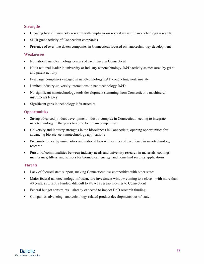
22
Strengths
• Growing base of university research with emphasis on several areas of nanotechnology research
• SBIR grant activity of Connecticut companies
• Presence of over two dozen companies in Connecticut focused on nanotechnology development
Weaknesses
• No national nanotechnology centers of excellence in Connecticut
• Not a national leader in university or industry nanotechnology-R&D activity as measured by grant and patent activity
• Few large companies engaged in nanotechnology R&D conducting work in-state
• Limited industry-university interactions in nanotechnology R&D
• No significant nanotechnology tools development stemming from Connecticut’s machinery/ instruments legacy
• Significant gaps in technology infrastructure
Opportunities
• Strong advanced product development industry complex in Connecticut needing to integrate nanotechnology in the years to come to remain competitive
• University and industry strengths in the biosciences in Connecticut, opening opportunities for advancing bioscience-nanotechnology applications
• Proximity to nearby universities and national labs with centers of excellence in nanotechnology research
• Pursuit of commonalities between industry needs and university research in materials, coatings, membranes, filters, and sensors for biomedical, energy, and homeland security applications
Threats
• Lack of focused state support, making Connecticut less competitive with other states
• Major federal nanotechnology infrastructure investment window coming to a close—with more than 40 centers currently funded, difficult to attract a research center to Connecticut
• Federal budget constraints—already expected to impact DoD research funding
• Companies advancing nanotechnology-related product developments out-of-state.

23
Section III. Strategic Framework for Connecticut in Nanotechnology Development
This report provides a comprehensive examination of the significance and relative position of Connecticut in nanotechnology, revealing specific strengths, weaknesses, threats, and opportunities for Connecticut. Based on this comprehensive review and analysis, this section of the report lays out a strategic framework for Connecticut to guide future investments and activities in nanotechnology.
A principal foundation of Connecticut’s leading position in the global knowledge-based economy has been its extensive capacities in advanced product development. As detailed in a recent study on Connecticut’s Core Competencies for the Knowledge Economy, sponsored by the Office of Workforce Competitiveness, Connecticut manufacturing-related companies compete based on their ability to design, develop, produce, and market a broad range of innovative, complex products, requiring significant systems integration skills, using advances in a wide range of technologies—from materials to information technology to electromechanical to optics-related to electrochemical.
Looking to the future, Connecticut will succeed in maintaining its advanced product capabilities by becoming a leading center for the integration of nanotechnology into a broad range of existing and new products, such as novel new materials and coatings, advanced engines, optoelectronic devices, factory systems, testing and measuring equipment, fuel cells, novel detection and sensor systems, advanced drug delivery approaches, and regenerative medical treatments, among many others.
Despite the significance of nanotechnology to Connecticut’s future competitiveness in advanced product development, a comprehensive review of the state’s position in nanotechnology suggests that Connecticut will be highly impacted by nanotechnology in the future, but is lagging behind in its current activities. Near-term investments are imperative for Connecticut to participate more actively in the advancement of nanotechnology.
A SITUATIONAL ASSESSMENT Connecticut is clearly playing catch-up in establishing a targeted nanotechnology capacity; the stakes are high if Connecticut is to retain its well-regarded leadership in advanced product development.
• Nanotechnology can be expected to have a broad reach across the existing industry base of Connecticut. Industries in which Connecticut has long enjoyed significant economic success and specialization will need to integrate and advance their capabilities in nanotechnology. For instance, nanotechnology-based coatings are making in-roads in the harsh environment of turbine engines and in other defense applications, nanotechnology-enabled sensors and filters are being developed for medical instruments and homeland security applications, and new drug delivery mechanisms and therapies are taking advantage of unique nanoscale phenomena. Based on detailed industry-by-industry profiles of the expected impact of nanotechnology on sales revenue, up to 27 percent of Connecticut’s goods producing sector (or just over 30,000 jobs) will be impacted by 2014. Failure to make this transition to nanotechnology will place a significant portion of Connecticut’s industry base at risk.

24
• Today Connecticut universities are active in nanotechnology research, but have not reached the critical mass and focus to support a major federally funded nanotechnology research center. Connecticut, in part, lags behind because it does not have a major federal lab in its borders to jump-start nanotechnology research as in New Mexico, Tennessee, Illinois, and New York. The importance of a having a national nanotechnology research center goes beyond the prestige they offer a state. Having a federal center of excellence serves as a magnet for promising faculty and students of nanotechnology, often provides a unique shared-use facility that attracts broader industry and university collaborations, and creates a platform for generating additional federal support.
• Key areas of university research that show significant strength and promise in the near term are in nanomaterials and the interface of biosciences and nanotechnology and, for the longer term, in areas of nanoelectronics. In nanomaterials, Connecticut’s university research base is engaged in advancing carbon nanotubes, nanoparticles, and nanoelectronics with broad applications for unique coatings, new materials, smaller and more robust electronic and computer devices, improved combustion technologies, inks with novel characteristics, and fuel cells. In bioscience-related nanotechnology, Connecticut’s research efforts are engaged in biosensors, tissue engineering, and drug delivery and benefit from the state’s strong university and industry biomedical research cluster. Optoelectronics, a particular area of nanoelectronics where Connecticut’s research base is focusing, is compatible with the state’s long-standing industry strengths in optics.
• Connecticut is not a “hot spot” of industry nanotechnology activity. On a positive note, this study identifies over two dozen companies in Connecticut where nanotechnology and nanoscale phenomena currently impact the research, development, intellectual property, products, and near-term business functions and opportunities. Yet, for the most part, the remaining Connecticut companies are not actively engaged in nanotechnology activities. Moreover, many Connecticut companies engaged in nanotechnology are actually conducting this work in their own out-of-state research laboratories or with key partners outside of Connecticut. Finally, the vast majority of Connecticut companies needing to integrate nanotechnologies as they advance are acting as spectators rather than participants. The key question is whether Connecticut companies will be able to gain the skill sets and knowledge of advancing nanotechnology and whether that activity will take place in Connecticut.
• Connecticut is being outflanked by other states because it lacks an investment program. Other states have actively targeted investments to establish a focus of nanotechnology research that can enable their universities to build the capacity to attract these federal nanotechnology research centers. These states often directly invest matching funds to win these federal research centers. Connecticut is largely absent in its investments in nanotechnology, and even areas of funding that would have the potential to advance nanotechnology—such as through the Clean Energy Fund—are not being tapped.
VISION AND MISSION FOR CONNECTICUT IN NANOTECHNOLOGY Connecticut by 2015 will be recognized as a leading state in the development and application of nanotechnologies to advance new products by existing and newly formed companies anchored by a set of well-established nanotechnology research and education assets across its public and private colleges and universities.
To succeed, Connecticut will establish a proactive capacity for industry to collaborate with colleges and universities in identifying and applying nanotechnology-related innovations discovered in-state and from across the world to existing and new markets.

25
Connecticut will be known as having a world-class infrastructure of specialized facilities to invent, develop, and test new nanotechnology-related applications, along with the research and educational capacities to generate the needed talent pool in nanotechnology skills to develop and attract industry activities.
PROPOSED FIVE-YEAR ACTION PLAN TO MOVE CONNECTICUT FORWARD Over the next five years, Connecticut requires a sustained and forward-looking action plan in nanotechnology. The state cannot expect to match the leading states within this period, but can lay the groundwork for raising its competencies in nanotechnology with the following objectives:
• Establishing a critical mass of research activity in nanotechnology able to garner national recognition as a research center of excellence in particular domains of nanomaterials and nanobiotechnology
• Engaging more broadly Connecticut’s advanced industrial base in developing nanotechnology applications, as demonstrated by active industry–university collaborations based in Connecticut and the location of industry labs focusing on nanotechnology development in the state.
Seven Priority Actions
An initial set of seven priority actions is proposed to achieve these goals. These first steps will point to broader and more substantial investment opportunities in the years ahead. But, having these initial investments in place and sustained over a five-year period will be the most critical steps taken by Connecticut.
The seven initial priority actions are as follows:
• Establishing a state-of-the-art Connecticut Nanotechnology Characterization Facility in a central location to serve Connecticut public and private colleges and universities and industry from across the state. The value of a characterization laboratory is that it is the starting point for developing, measuring, and testing nanotechnology applications through the use of advanced atomic-level instrumentation, whether related to academic research or industrial product development. While a nanotechnology-characterization facility is expected to generate substantial user fees from university and industry activities to support its ongoing operations, a substantial up-front investment is required to fund the acquisition of advanced instrumentation and construction of a specialized facility to house the equipment, as well as to cover the start-up operating costs. Based on initial discussions with leading nanotechnology researchers on appropriate instrumentation and programs to be housed within a proposed nanotechnology-characterization facility, the upfront investment could reach $25 to $35 million. The importance of this investment cannot be underestimated. The presence of the Connecticut Nanotechnology Characterization Facility is expected not only to be a key resource for attracting additional federal funding in nanotechnology research, including a federally funded research center, but to be a key resource for Connecticut industry as it turns toward integrating nanotechnology into its ongoing product development activities.
• Retain and recruit entrepreneurial, Eminent Scholars in nanotechnology across colleges and universities in Connecticut. Excellence in nanotechnology research depends upon the quality of research talent in the state. Eminent Scholar initiatives have been a key tool for states across the nation in establishing leading research programs. Eminent Scholars bring a team of researchers involving junior faculty, post-doctorate fellows, technicians, and graduate students, and represent a

26
major infusion of talent. For Connecticut, endowed chairs not only will attract key research expertise to fill gaps among existing researchers, but will retain the top research talent already in Connecticut. Connecticut should require that these Eminent Scholars demonstrate not only a track record of outstanding research accomplishments, but industry collaborations and commercialization. These endowed chairs in nanotechnology should be bid competitively at all public and private colleges and universities that are able to apply, with the understanding that they will be filled by Connecticut scholars who are expected to collaborate with academic colleagues and industry from across the state. As part of the selection process to determine which colleges and universities host these endowed chairs, the level of matching funds, integration into a research program, and collaborations with other colleges and universities in Connecticut should be taken into account.
• Provide seed grants targeted to nanotechnology for multi-institutional research collaborations and industry R&D partnerships with colleges and universities. A sustained five-year seed fund should be established in Connecticut to promote multi-institutional academic collaborations advancing the development and application of nanotechnology and supporting matching funds for industry R&D partnerships with Connecticut research faculty. The seed grants should be at the $50 to $75 thousand level each, with simplified application and reporting requirements and a goal of 25 to 50 per year—or $2 to $3 million annually—to stimulate more nanotechnology research and create a more collaborative environment for such research. The goal of these seed funds is to obtain the initial pilot results to obtain larger federally funded projects and to demonstrate proof-of-concept for more extensive industry collaborations with colleges and universities in Connecticut. It is expected that much of these seed grants will support graduate students and post-doctoral fellows.
• Develop a Strategic Matching Fund of $15 to $25 million for future applications for federally funded nanotechnology research centers. Connecticut colleges and universities need to have a predictable source of matching funds for future applications for federally funded nanotechnology research centers. As a requirement to access these matching funds, it is proposed that they involve a Connecticut college or university as a lead, have at least one other college or university involved in a meaningful role, and have Connecticut industry collaborations that involve a significant engagement.
• Establish a Technical Nanotechnology Forum that can be a peer-to-peer network for scientists and engineers involved in nanotechnology R&D in the state across the broad base of higher education and industry. Connecticut needs to be more proactive in bringing the community of scientists and engineers in nanotechnology together. This can include developing resource directories with details on research expertise, interests, and laboratory resources to encourage partnerships; hosting seminars with leading experts from across the world in nanotechnology; and creating specialized programs for graduate students and post-doctoral fellows to establish relationships with Connecticut companies.
• Create a Nanotechnology Education Clearinghouse to sponsor curriculum development, support professional development of teachers, and encourage access to specialized instructional labs. Education and training in nanotechnology need to be stimulated in Connecticut. Nanotechnology must be integrated more extensively into associate’s, bachelor’s, and master’s degrees, and not simply left to Ph.D. programs. A number of Connecticut higher education institutions are already engaged in developing a nanotechnology curriculum. The goal should be to share approaches, fill needed gaps in curriculum development, and address access to instructional laboratories across higher education.

27
Figure 3. Integrative and Reinforcing Aspects of Proposed Nanotechnology Action Steps for Connecticut
As specific industry needs emerge, the Clearinghouse can also help sponsor more targeted nanotechnology program development to equip incumbent and potential workers to meet the needs of industry for a technically trained nanotechnology workforce.
• Establish proof-of-concept funding to advance nanotechnology discoveries and validate their potential for commercialization, with active linkage to pursuing federal SBIR funds. Nanotechnology research across higher education is reaching the critical mass in Connecticut, calling for more proactive efforts to advance its commercial application. What holds back many research discoveries is validating their feasibility beyond the bench. Specific reduction to practice for high-potential commercial applications is needed to attract existing industry or venture capital interest. Having a nanotechnology proof-of-concept fund would create a predictable path for moving from the research laboratory to more commercial settings.
This proof-of-concept funding can help leverage and work in combination with federal SBIR funding by providing the pre-SBIR funding needed to demonstrate that the concept has commercial potential, and then to fill gaps in the timing of receiving federal assistance.
Individually, these seven actions are important steps to strengthen Connecticut’s competitive position in nanotechnology. But, together they can form a highly integrated and reinforcing approach in which each action serves as a resource or a generator of demand for the other actions, as suggested in Figure 3.
Approaches to Implementing the Proposed Action Steps
If implemented as a dedicated nanotechnology initiative, these seven action steps can serve as the backbone of a more focused “technology accelerator” in nanotechnology for Connecticut. The concept of a “technology accelerator” was envisioned by the Connecticut Technology Transfer and Commercialization Advisory Board of the Governor’s Competitiveness Council as “a focal point to coordinate various R&D, technology transfer, and entrepreneurial activities in the state” for defined areas of core competencies.
Seed Grants for Industry-University Collaborations
Strategic Matching Fundfor Federal Centers
Technical Nanotech Forum
Nano-CharacterizationFacility
Educational Clearinghouse
Proof-of-ConceptFunding
Entrepreneurial, EminentScholars
Key
Reso
urce
Key Resource
Key R
esour
ce Key Resource
Key Attraction to Recruit
Provide Industry Involvement
Source of IdeasSource of Opportunities
Source of Resources and Ideas
Source of Ideas Source of Ideas
Leading Contributors
Leading Contributors
Source of Ideas

28
Alternatively, these seven action steps can be pursued more independently, since many of the actions can be incorporated into either ongoing or broader initiatives supporting more than nanotechnology. For instance, nanotechnology can be just one of several technology targets for recruiting entrepreneurial Eminent Scholars to Connecticut or for proof-of-concept funding.
Once the choice of approach is determined, a full-scale prospectus or operating plan can be completed, involving more detailed implementation plans such as specifics on the design, resource requirements, lead organizations and milestones to be achieved.
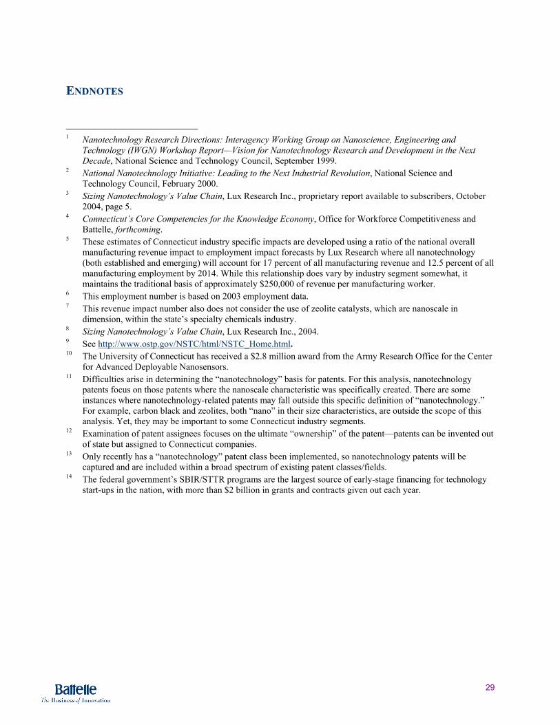
29
ENDNOTES
1 Nanotechnology Research Directions: Interagency Working Group on Nanoscience, Engineering and
Technology (IWGN) Workshop Report—Vision for Nanotechnology Research and Development in the Next Decade, National Science and Technology Council, September 1999.
2 National Nanotechnology Initiative: Leading to the Next Industrial Revolution, National Science and Technology Council, February 2000.
3 Sizing Nanotechnology’s Value Chain, Lux Research Inc., proprietary report available to subscribers, October 2004, page 5.
4 Connecticut’s Core Competencies for the Knowledge Economy, Office for Workforce Competitiveness and Battelle, forthcoming.
5 These estimates of Connecticut industry specific impacts are developed using a ratio of the national overall manufacturing revenue impact to employment impact forecasts by Lux Research where all nanotechnology (both established and emerging) will account for 17 percent of all manufacturing revenue and 12.5 percent of all manufacturing employment by 2014. While this relationship does vary by industry segment somewhat, it maintains the traditional basis of approximately $250,000 of revenue per manufacturing worker.
6 This employment number is based on 2003 employment data. 7 This revenue impact number also does not consider the use of zeolite catalysts, which are nanoscale in
dimension, within the state’s specialty chemicals industry. 8 Sizing Nanotechnology’s Value Chain, Lux Research Inc., 2004. 9 See http://www.ostp.gov/NSTC/html/NSTC_Home.html. 10 The University of Connecticut has received a $2.8 million award from the Army Research Office for the Center
for Advanced Deployable Nanosensors. 11 Difficulties arise in determining the “nanotechnology” basis for patents. For this analysis, nanotechnology
patents focus on those patents where the nanoscale characteristic was specifically created. There are some instances where nanotechnology-related patents may fall outside this specific definition of “nanotechnology.” For example, carbon black and zeolites, both “nano” in their size characteristics, are outside the scope of this analysis. Yet, they may be important to some Connecticut industry segments.
12 Examination of patent assignees focuses on the ultimate “ownership” of the patent—patents can be invented out of state but assigned to Connecticut companies.
13 Only recently has a “nanotechnology” patent class been implemented, so nanotechnology patents will be captured and are included within a broad spectrum of existing patent classes/fields.
14 The federal government’s SBIR/STTR programs are the largest source of early-stage financing for technology start-ups in the nation, with more than $2 billion in grants and contracts given out each year.

30

A-31
Appendix A. Connecticut Companies Actively Engaged in Nanotechnology R&D
and/or Product Development, by Value Chain Segment
Value Chain Segments Nanomaterials Nanointermediates Nano-enabled Products
Nanotechnology Tools Development
Description CT Companies
Nanoscale structures in unprocessed form such as nanoparticles, nanotubes, fullerenes, dendrimers, quantum dots, nanoporous materials, etc
Intermediate products with nanoscale features such as coatings, fabrics, memory and logic chips, contrast media, optical components, orthopedic materials, superconducting wire, etc.
Finished goods incorporating nanotechnology such as aerospace, devices, pharmaceuticals, computers, consumer electronics, etc.
Capital equipment (including analytic, characterization, and processing equipment) enabling the development or production of products with nanoscale features.
454 Life Sciences ASML (SVG Lithography) ATMI (Advanced Tech. Materials, Inc.) Cookson Electric (Enthone-OMI, Inc.) Crompton Corporation Cytec Technology Electric Boat (General Dynamics) Fuel Cell Energy General Electric IBM Inframat/U.S. Nanocorp Jet Process Corporation Kaman Aerospace KX Industries (Koslow) Loctite Corporation (Henkel) MGS Research M-Phase MysticMD NanoSciences Corporation Neurogen Corporation Ortronics, Inc. Pentron Corporation Pfizer Photronics Praxair Precision Combustion Real-Time Analyzer (RTA) United Technologies Corp. (incl. UTRC) Xerox
Source: Battelle Discussions, Connecticut Nanotechnology Initiative Survey, Lux Research, Freedonia, BCC, Corporate Information and Websites

A-32

B-33
Appendix B. Federal Agency Approaches as Part of the
National Nanotechnology Initiative
Following is a discussion, on an agency-by-agency basis, of activities in the National Nanotechnology Initiative (NNI) of the federal government. The list is in declining order of FY 2006 Presidential Budget Request as reported by NNI, although this may not necessarily indicate the true opportunity for partnership formation. Not all NNI dollars are competitive or uncommitted, but there may be chances to receive support for nanotechnology research and development (R&D) through programs that are not so designated—for example, the multifield Advanced Technology Program (ATP) at the Department of Commerce–National Institute of Standards and Technology (NIST). Below are some comments about each section of the profiles that follow:
• Nanotechnology Interests. In this section are interpretations of the connection between an agency’s mission and its expressed interest in nanotechnology R&D, and the organizational units that are responsible for funding decisions. Not only are intramural NNI dollars not available for open competition, but investigators at some intramural federal laboratories seem to compete for the same funding available to university investigators (this seems more common at the Department of Energy [DOE] or the National Aeronautics and Space Administration [NASA] than at the armed services laboratories).
• Existing Centers. In this section are names and links to all the centers referenced in the NNI strategic plan. This is important both because intramural centers account for NNI funding that is not competitively available and because the list of university-based centers (including user facilities) suggests that Connecticut is behind in establishing centers.
• Current Opportunities. This section provides links to the funding opportunities relevant to nanotechnology currently offered by each participating agency. In the case of the first few agencies, these opportunities may be specifically targeted to nanotechnology. In most of the smaller agencies, nanotechnology proposals will be considered as part of broader funding programs. In all cases, careful scrutiny is important to understand whether academicians and federal laboratory employees are in competition. Links are also provided to Small Business Innovation Research (SBIR) solicitations, which sometimes support cutting-edge science disproportionately to an entire agency’s R&D budget. Also, academicians may be used to the National Science Foundation (NSF) and the National Institutes of Health (NIH), where funding availability is announced by specific grant programs. Many federal agencies instead publish broad agency announcements (BAAs) of their general interest that remain open for some time and through which agencies may fund with grants, cooperative agreements, or contracts, depending on the nature of the respondent and the extent the proposed topic has public purpose versus being mission oriented. These announcements can be found on the individual agency Web sites or through two federal portals:
o www.fedbizopps.gov – The successor to the Commerce Business Daily, which lists all procurement opportunities (including BAAs that do not specify the contract mechanism) greater than $25,000.
B-34
o www.grants.gov – Lists all opportunities by BAA or program announcement where the contract mechanism has been definitely excluded, leaving only grants or cooperative agreements as possibilities.
• NSET Representatives. This section lists the agency representatives to the Nanoscale Science, Engineering and Technology (NSET) Subcommittee of the Committee on Technology of the National Science and Technology Council. These representatives are usually at the working level in the agencies, and they seem to change frequently. They are mostly not policymakers themselves nor do they necessarily manage competitive programs (although some do). However, they are excellent sources of insight into agency priorities. Their names and contact information are not confidential, though are sometimes difficult to find in one place.
• Assessment. Each agency profile concludes with an assessment of the strategic importance of the agency to a potential Connecticut nanotechnology strategy.
A Note on Earmarks. The Congressional Research Service has observed that there is no standard practice for earmarking; and, in some sense, every appropriation that gives detail within a budgetary account is an earmark.1 Typically, they are designated through statements accompanying appropriations or conference committee reports. Analysis by the American Association for the Advancement of Science (AAAS) of the FY 2005 omnibus appropriations bill (encompassing $132 billion in federal R&D) suggests2 that R&D earmarks totaled $2.1 billion, concentrated in four agencies: the U.S. Department of Agriculture (USDA), National Academy of Sciences (NAS), DOE, and the Department of Defense (DoD). Overall, the share of the federal R&D portfolio earmarked was 1.6 percent, but in certain programs was as high as 20 to 25 percent. AAAS notes that DoD is growing so rapidly that it is the obvious best target. Most DoD R&D earmarks are small ($10 million or less) and typically in the “R” rather than “D” parts of the budget. AAAS reports that certain agencies (NSF, NIH, and the Department of Homeland Security [DHS]) have remained earmark-free.
1 Congressional Research Service. Library of Congress. “Earmarks and Limitations in Appropriations Bills.” CRS Report 98-518. Available on-line from http://www.ncseonline.org/NLE/CRSreports/government/gov-21.cfm?&CFID=18086272&CFTOKEN=8154731. 2 AAAS R&D Budget and Policy Program. American Association for the Advancement of Science. Congressional Action on Research and Development in the FY 2005 Budget. Washington, D.C.: AAAS, 2004. Available on-line at http://www.aaas.org/spp/rd/ca05main.htm.
B-35
NATIONAL SCIENCE FOUNDATION ($344 MILLION)
Nanotechnology Interests
NSF is the undisputed lead agency in the NNI, with interests ranging across every directorate and relatively large expenditures in the directorates covering physical sciences, engineering, and computer and information science. NSF lists primary interest in five of seven program component areas (PCAs) (the most of any NNI agency): fundamental nanoscale phenomena and processes, nanomaterials, nanomanufacturing, research facilities and instrumentation, and societal dimensions. NSF has set up a coordinating Nanoscale Science and Engineering Group, with two representatives from each NSF directorate. The agency breaks down its commitment for FY 2005 as follows:
• Fundamental research and education, $174 million
• “Grand challenges,” $11.9 million
• Centers and Networks of Excellence (university-based), $57.5 million
• Research infrastructure, $36.9 million
• Societal/educational implications, $24.7 million
• National Nanotechnology Infrastructure Network, $15 million
• Network for Computational Nanotechnology, $3 million.
Considerable amounts of this funding are pre-committed to existing multiyear center awards.
Existing Centers
NSF’s base of existing centers falls into three categories.
National Nanofabrication Infrastructure Network3
This network of 13 nodes evolved from the five-node Nanofabrication User Network. It comprises facilities of some standing, including those with roots in microelectronics or MEMS research. These are user facilities: investigators nationwide who pass peer review are welcome to use time, although unlike at DOE’s user facilities, they must use their own grant funds to pay certain charges, which are subsidized but not entirely erased by NSF support to the user facility. These facilities have often been leveraged by universities to obtain other major grants from NSF, other federal agencies, or state agencies. For example, at Cornell, investigators obtained a separate NSF Science and Technology Center grant for Nanobiotechnology.4 The complete list of NNIN nodes is as follows:
• Cornell Nanoscale Facility5
• Stanford Nanofabrication Facility6
• Solid State Electronics Laboratory7 at the University of Michigan
3 See http://www.nnin.org/. 4 See http://www.nbtc.cornell.edu/. 5 See http://www.nnin.org/nnin_cornell.html. 6 See http://www.nnin.org/nnin_stanford.html. 7 See http://www.nnin.org/nnin_michigan.html.

B-36
• Micro-electronics Research Center8 at Georgia Tech
• Center for Nanotechnology9 at the University of Washington
• Penn State Nanofabrication Facility10
• Nanotech11 at the University of California, Santa Barbara (UCSB)
• Minnesota Nanotechnology Cluster12 at the University of Minnesota
• Nanoscience13 at the University of New Mexico
• Microelectronics Research Center14 at the University of Texas at Austin
• Center for Imaging and Mesoscale Structures15 at Harvard
• Howard Nanoscale Science and Engineering Facility16
• Triangle National Lithography Center17 at North Carolina State University (NCSU).
Network for Computational Nanotechnology18
Purdue is the central node for this algorithm-development initiative, which also involves researchers at Northwestern, Morgan State, and Stanford, as well as the universities of Florida, Illinois, and Texas-El Paso.
Nanoscale Science and Engineering Centers (NSECs)
These are multiyear, large centers at the scale of NSF’s other centers, such as the Science and Technology Centers, the Engineering Research Centers, or the Materials Research Science and Engineering Centers (of which 19 out of 28 are also listed as having nanotechnology content). Below are the NSECs that have been awarded to date:
• Center for Nanoscale Systems in Information Technology19 at Cornell
• Center for Integrated Nanopatterning and Detection20 at Northwestern
• Nanoscale Systems and Device Applications21 at Harvard
• Center for Electronic Transport in Molecular Nanostructure22 at Columbia
8 See http://www.nnin.org/nnin_georgiatech.html. 9 See http://www.nnin.org/nnin_washington.html. 10 See http://www.nnin.org/nnin_psu.html. 11 See http://www.nnin.org/nnin_ucsb.html. 12 See http://www.nnin.org/nnin_minnesota.html. 13 See http://www.nnin.org/nnin_newmexico.html. 14 See http://www.nnin.org/nnin_texas.html. 15 See http://www.nnin.org/nnin_harvard.html.. 16 See http://www.nnin.org/nnin_howard.html. 17 See http://www.nnin.org/nnin_ncsu.html. 18 See http://ncn.purdue.edu/. 19 See http://www.cns.cornell.edu/index.html. 20 See http://www.nsec.northwestern.edu/. 21 See http://www.nsec.harvard.edu/. 22 See http://www.cise.columbia.edu/nsec/index.html.
B-37
• Directed Assembly of Nanostructures23 at Rensselaer Polytechnic Institute
• Center for Scalable and Integrated NanoManufacturing24 at the University of California, Los Angeles (UCLA)
• Center for Chemical-Electrical-Mechanical Manufacturing Systems25 at the University of Illinois at Urbana-Champaign
• Center for Integrated Nanomechanical Systems26 at the University of California, Berkeley
• Center for High-Rate Nanomanufacturing27 at Northeastern
• Center for Affordable Nanoengineering of Polymer Biomedical Devices28 at The Ohio State University
• Center for Molecular Function at the Nano/Bio Interface29 at the University of Pennsylvania
• Center for Probing the Nanoscale30 at Stanford
• Center on Templated Synthesis and Assembly at the Nanoscale31 at the University of Wisconsin-Madison.
Current Opportunities
NSF research opportunities in nanotechnology are consolidated in a single, comprehensive program announcement: http://www.nsf.gov/pubs/2004/nsf04043/nsf04043.htm, with a separate announcement for education grants: http://www.nsf.gov/pubs/2005/nsf05543/nsf05543.htm. The agency’s SBIR grants are run by the Engineering Directorate’s Division of Design, Manufacture and Industrial Innovation; and opportunities may be found at: http://www.eng.nsf.gov/sbir/.
NSET Representatives
• Dr. Maryanna Henkart, Director, Division of Molecular and Cellular Biology, Directorate for Biological Sciences, (703) 292-8440. [email protected].
• Dr. Mihail C. Roco, Senior Advisor for Nanotechnology, Directorate for Engineering, (703) 292-8301. [email protected].
• Dr. Thomas A. Weber, Director, Division of Materials Research, Directorate for Mathematical and Physical Sciences, (703) 292-4915. [email protected].
23 See http://www.rpi.edu/dept/nsec/. 24 See http://newsroom.ucla.edu/page.asp?id=4601. 25 See http://www.news.uiuc.edu/news/03/1009nano.html. 26 See http://nano.berkeley.edu/coins/coins.htm. 27 See http://www.nano.neu.edu/aboutus.html. 28 See http://www.nsec.ohio-state.edu/index1.htm. 29 See http://www.nanotech.upenn.edu/. 30 See http://news-service.stanford.edu/news/2004/october6/moler-106.html. 31 See http://www.nsec.wisc.edu/.

B-38
Assessment
NSF is the agency of choice for academic researchers interested in nanotechnology because its range of interest is broad, the amount of uncommitted money is significant even after precommitted funds, and there are no ties to any intramural government laboratories that would disfavor Connecticut. However, Connecticut institutions have been slow to compete for existing centers, many of which are multiyear awards. Substantial effort should be made to develop relationships with the relevant program officers, receive debriefings on any failed proposals, and ensure that proposals from Connecticut institutions are responsive and enjoy strong state support.

B-39
DEPARTMENT OF ENERGY ($230 MILLION)
Nanotechnology Interests
DOE is a mission-driven agency, with a strong historic commitment to fundamental research in the physical sciences. Of the department’s seven major strategic goals, the fifth is “world class scientific research capacity.” This work is expressed both through the network of national laboratories reporting to the Office of Science32 and the headquarters Office of Basic Energy Sciences (BES), a coordinator of competitive funding.33 The Office of Science now lists nanoscale science as a top priority within the “research capacity goal”34 and estimates that its support accounts for about a quarter of all nanoscale research nationally, both in the university and federal laboratory sector. The Office is interested in nanotechnology as a fundamental underpinning for a broad range of envisioned advances in energy efficiency. Overall, DOE lists primary interest in three PCAs: fundamental nanoscale phenomena, nanomaterials, and major research facilities and instrumentation. The BES office serves as NNI coordinator and has published its own review of the department’s research directions at the nanoscale.35
Existing Centers
The main expression of the NNI at DOE to date has been the creation of a network of laboratory-based Nanoscale Research Centers.36 These are “user facilities” on the traditional DOE model: the Department constructs a laboratory building on the campus of a national laboratory, usually adjacent to a unique scientific resource such as a neutron or energetic photon source. The program subsidizes basic operating costs so that investigators who pass peer review are permitted access without charge so long as they intend to publish in the open literature. Proprietary projects are accommodated at full cost recovery. Below is the list of centers created to date:
• Center for Functional Nanomaterials37 at Brookhaven National Laboratory, just across the Long Island Sound in New York
• Center for Integrated Nanotechnologies38 at Sandia National Laboratories and Los Alamos National Laboratories, both in New Mexico
• Center for Nanophase Materials Science39 at Oak Ridge National Laboratory in Tennessee
32 See http://www.sc.doe.gov/sub/organization/organization.htm. 33 See http://www.sc.doe.gov/feature/BES.htm. Note that laboratories compete with universities for this funding. 34 U. S. Department of Energy. Office of Science. Strategic Plan: February 2004. Available on-line at http://www.science.doe.gov/bes/SCSP_12FEB04.pdf. 35 U. S. Department of Energy. Office of Science. Nanoscale Science, Engineering and Technology in DOE’s Office of Basic Energy Sciences: Research Directions and Nanoscale Science Research Centers. Prepared by Oak Ridge National Laboratory, February 2003. Available on-line at http://www.science.doe.gov/bes/brochures/files/NSRC_brochure.pdf. 36 See http://www.science.doe.gov/bes/BESfacilities.htm. 37 See http://www.cfn.bnl.gov/. 38 See http://cint.lanl.gov/. 39 See http://www.cnms.ornl.gov/.

B-40
• Center for Nanoscale Materials40 at Argonne National Laboratory near Chicago
• Molecular Foundry41 at Lawrence Berkeley Laboratory in California.
Current Opportunities
Office of Science competitive opportunities are posted at http://www.sc.doe.gov/grants/grants.html. SBIR opportunities are at http://sbir.er.doe.gov/sbir/.
NSET Representatives
• Dr. Kristin A. Bennett, Division of Materials Sciences and Engineering, Office of Basic Energy Sciences, (301) 903-4269. [email protected].
• Dr. Altaf H. Carim, Division of Materials Sciences and Engineering, Office of Basic Energy Sciences, (301) 903-4895. [email protected].
• Dr. Patricia M. Dehmer, Director, Office of Basic Energy Sciences, (301) 903-3081. [email protected].
• Dr. Aravinda Kini, Division of Materials Sciences and Engineering, Office of Basic Energy Sciences, (301) 903-3565. [email protected].
• Dr. John C. Miller, Division of Chemical Sciences, Geosciences, and Biosciences, Office of Basic Energy Sciences, (301) 903-5806. [email protected].
• Dr. Brian G. Valentine, Office of Industrial Technologies, (202) 586-1739. [email protected].
Assessment
DOE represents one of the single strongest opportunities for nanotechnology research support at the fundamental level, albeit motivated by mission goals. The strength of Connecticut’s alternative-energy sectors suggests major opportunities to build the underlying science base through cooperation with DOE program managers at either BES or the national laboratories or both. However, the national laboratories are primarily “sinks” rather than “sources” for funds and are useful partners only if their involvement qualifies a project for additional funding administered by DOE headquarters.
40 See http://nano.anl.gov/. 41 See http://foundry.lbl.gov/program/program.html.

B-41
DEPARTMENT OF DEFENSE ($207 MILLION)
Nanotechnology Interests
DoD’s overall science and technology strategy is aimed explicitly at long-term mission goals such as information assurance, battlespace awareness, force-protection, and reduced cost of ownership. However, the Department has long recognized an underlying need for strong basic research, including a steady flow of trained scientists and engineers for government and industry.42 As an early-stage science, nanotechnology plays an important role in the exploratory agendas of both Defense Advanced Research Projects Agency (DARPA)43—the centralized manager of advanced extramural research—and the services’ own research laboratories and their coordinating offices,44 which have both intramural and extramural programs. In fact, nanoscience is one of six strategic research areas for the service laboratories, cross-cutting the disciplinary areas of physics, chemistry, computer sciences, electronics, materials science, and biological sciences.45 Within DARPA, there is also nanotechnology interest across the board, in both the Defense Sciences Office and the Advanced Technology Office. DoD lists primary interest in three PCAs: nanomaterials, nanoscale systems and devices; and major research facilities and instrumentation. It should also be noted that as one of the fastest-growing federal budgets, Defense is a natural site for “earmarks,” which will certainly be used aggressively to support nanotechnology facilities and research nationwide.
Existing Centers
DoD was one of the earliest agencies to provide strong funding leadership in nanotechnology. In FY 2001, the first year of the NNI, the Department made 16 nanoscience awards to universities through its Defense University Research Initiative on Nanotechnology (DURINT) (not one to a Connecticut investigator)46 and another five on nanotechnology topics through the Multidisciplinary University Research Initiative (MURI) (also none to Connecticut investigators).47 All expire this year, subject to renewal. Last year, DoD funded three major centers, two through competitive extramural competitions and one intramurally:
• Institute of Soldier Nanotechnologies at the Massachusetts Institute of Technology (MIT),48 a five-year, $50 million contract from the U.S. Army Research Office (Durham) aimed at technology for improving the survival of soldiers. Seven teams focus on energy-absorbing materials; mechanically active materials and devices; sensing and counteraction; biomaterials and nanodevices for medical technology; processing and characterization (nanofoundries); modeling and simulation of materials and processes; and systems design, hardening, and integration. The founding partners are Raytheon,
42 U.S. Department of Defense. Deputy Undersecretary of Defense for Science and Technology. “Defense Science and Technology Strategy,” May 2000. Available on-line at http://www.wslfweb.org/docs/dstp2000/Strategy.pdf. 43 See http://www.darpa.mil/. 44 Office of Naval Research/Naval Research Laboratory (NRL); Air Force Office of Scientific Research/Air Force Research Laboratory; Army Research Office/Army Research Laboratory. 45 See http://www.dod.mil/ddre/labs/basic_research.html#Areas. A cross-cutting list of extramural funding program managers prepared by NRL can be found at http://nanosra.nrl.navy.mil/funding.php. 46 See http://www.defenselink.mil/news/Feb2001/d20010223durint.pdf. Also 17 accompanying equipment grants at http://www.defenselink.mil/news/Feb2001/d20010223equip.pdf. 47 See http://www.dod.mil/news/Feb2001/d20010202muri.pdf. 48 See http://www.web.mit.edu/isn/aboutisn/index.html.

B-42
DuPont, and Partners Healthcare, with additional members of an industry consortium. The Institute has dozens of involved faculty and visitors.
• Center for Nanoscience Innovation in Defense, a three-year, $20 million program embedded in the California NanoSystems Institute,49 a state-funded collaboration of UCSB and UCLA with participation from the University of California at Riverside. The DoD funding is being used to equip state-funded facilities with instrumentation and for graduate fellowships. The focus is on production of basic research talent. There is strong participation from defense contractors such as Boeing, DuPont, Hewlett-Packard, Hughes, Motorola, NanoSys, Northrop Grumman, Rockwell, Raytheon, and TRW.
• Institute for Nanoscience, an intramural multidisciplinary effort based at the NRL in Washington, D.C.50
Current Opportunities
While the DURINT competition has not been repeated per se, there are nanotechnology opportunities from time to time within the University Research Initiatives program, especially the MURI, and the Defense University Research Instrumentation Program. Both are multiagency programs whose interests are announced through BAAs cross-referenced through the service laboratories’ own Web sites, where links to SBIR opportunities also can be found.
• http://www.aro.army.mil/research/index.htm
• http://www.onr.navy.mil/02/business_opp.asp
• http://www.afosr.af.mil/oppts/afrfund.htm
• http://www.darpa.mil/baa
In some of the services, both the office and the laboratory issue their own BAAs, while in others the office issues a BAA on behalf of the entire organization. There is also variation on whether the laboratory reports to the office or the office is a coordinating unit of the laboratory. However, in general, it is true that DoD intramural laboratories are more sources and less sinks of funding than other federal agency laboratories and are less likely to compete against academic researchers.
NSET Representatives
• Dr. William O. Berry, Director for Basic Research, DoD Office of the Deputy Undersecretary for Laboratories and Basic Sciences, (703) 696-0363. [email protected].
• Dr. James S. Murday, Acting Chief Scientist, Office of Naval Research, (703) 696-6783. [email protected].
• Dr. Gernot Pomrenke, Directorate of Physics and Electronics, Air Force Office of Scientific Research, (703) 696-8426. [email protected].
• Dr. David Stepp, Army Research Office, (919) 549-4329. [email protected].
49 See http://www.cnsi.ucla.edu/mainpage.html. 50 See http://www.nrl.navy.mil/content.php?P=MULTIDISCIPLINE.

B-43
Assessment
With Connecticut’s strong defense-contracting sector, there would seem to be ample opportunity to respond to opportunities presented by DoD constituent agencies. It is of critical importance that DoD sees basic research as part of a continuum that leads to demonstration and development and finally to procurement opportunities (Figure B-1 is a diagram from an Air Force Research Laboratory document, but would apply equally to the other service laboratories). Every chance should be taken to build excitement about research that could lead to products demanded by DoD program managers and that could be sold by Connecticut defense companies. The DoD SBIR program has been extremely active in nanotechnology, especially in topics posed by the Air Force, and should be considered a major opportunity.
Figure B-1. Science and Technology Program Structure
B-44
NATIONAL INSTITUTES OF HEALTH ($147 MILLION)
Nanotechnology Interests
The NIH strategic roadmap has a specific subsection devoted to nanomedicine,51 defined as a “medical intervention at the molecular scale for curing disease or repairing damaged tissues…” NIH has created its own internal implementation group that includes not only its NSET representatives, but also many others from across the institutes. Allocations of the NNI budget will be made both to intramural programs and extramurally by multiple institutes, with efforts loosely coordinated by the NIH Bioengineering Consortium (BECON).52 The institute that seems furthest advanced in its individual plans is the National Cancer Institute (NCI), which has launched an Alliance for Nanotechnology in Cancer,53 described as a five-year, $144.3 million initiative that will start by allocating $20 million in FY05 to create three to five university-based Centers for Cancer Nanotechnology Excellence. NIH lists primary interest in two PCAs: fundamental nanoscale processes and nanoscale devices and systems.
Existing Centers
NIH is still attempting to create its first university-based centers. However, intramurally, NCI cosponsors with NIST a Nanotechnology Characterization Laboratory for Cancer Research.54
Current Opportunities
A solicitation is open for nanomedicine development centers, envisioned as multidisciplinary, university-based centers staffed by biologists, physicians, physical scientists, mathematicians, engineers, and computer scientists. Dr. Leslie Low of the University of Connecticut (UCONN), having won a concept development award, is one of 20 investigators nationwide eligible to apply. Also, Dr. Steven Goldstein of Yale was one of several academicians invited to present before the project launch meeting of the nanomedicine roadmap initiative (he spoke on ion channels as “nano-mediators” of health, disease, and therapy).55 Major opportunities are as follows:
• The NCI Cancer Nanotechnology Alliance: http://nano.cancer.gov/funding_grants.asp with the “center” RFA at http://grants.nih.gov/grants/guide/rfa-files RFA-CA-05-024.html.
• Cross-institute awards for nanoscience and nanotechnology in biology and medicine at http://grants.nih.gov/grants/guide/pa-files/PAR-03-045.html.
• Nanotechnology topics in SBIR at http://grants.nih.gov/grants/guide/pa-files/pa-02-125.html.
• BECON also maintains links to other NIH programs that will entertain nanotechnology proposals.
NSET Representatives
• Dr. Eleni Kousvelari, Chief, Cellular and Molecular Biology, Physiology and Biotechnology Branch, Institute of Dental and Craniofacial Research, (301) 594-2427. [email protected].
51See http://nihroadmap.nih.gov/nanomedicine/index.asp. 52 See http://www.becon.nih.gov/nano.htm. 53See http://nano.cancer.gov/. 54 See http://nano.cancer.gov/nanotech_ncl.asp. 55 See http://nihroadmap.nih.gov/nanomedicinelaunch/pdf/Session_I_Goldstein.pdf.
B-45
• Dr. Jeffery A. Schloss, Program Director, Technology Development Coordination, National Human Genome Research Institute, (301) 496-7531. [email protected].
Assessment
Connecticut seems as well positioned as many states to advance its interests in nanotechnology with a biomedical approach and should be sure not to forfeit its early advantage with NIH even if its proposal for a nanomedicine development center does not succeed. There seem to be ample opportunities in SBIR as well.

B-46
NATIONAL INSTITUTE OF STANDARDS AND TECHNOLOGY ($75 MILLION)
Nanotechnology Interests
NIST sees nanotechnology as an enabling technology pertinent to its core mission of measurement and standard-setting and understands that it needs to keep these capabilities current with the reduction of industrial processes to the nanoscale. The agency reports that about half its NNI budget will be allocated intramurally among NIST laboratories through a competitive process and half will be competed externally among both universities and other government agencies that have the expertise necessary for the mission. NIST lists primary interest in two PCAs: instrumentation, research, and metrology and nanomanufacturing.
Existing Centers
NIST is organized into a series of specialized laboratories divided between Gaithersburg, Maryland, and Boulder, Colorado. Probably a dozen such laboratories have a significant nanotechnology interest or capability, but the important new center whose funding was justified in part through an NNI linkage is the Advanced Measurement Laboratory,56 a major expansion and modernization of the main campus in Gaithersburg, Maryland.
Current Opportunities
The most likely opportunities are through NIST’s precision measurement program at http://physics.nist.gov/ResOpp/grants/grants.html. Materials science and engineering grants are currently unfunded. Nanotechnology proposals have also been entertained through the industry-oriented ATP: http://www.atp.nist.gov/. SBIR opportunities are at http://patapsco.nist.gov/ts_sbir/.
NSET Representatives
• Dr. Alamgir Karim, Polymers Division, (301) 975-4924.
• Dr. Michael Postek, Program Analyst, NIST Program Office, (301) 975-4525. [email protected].
• Dr. Robert D. Shull, Metallurgy Division, (301) 975-2660. [email protected].
Assessment
If Connecticut’s advanced materials and precision manufacturing sectors can organize themselves to serve the identified needs of NIST, there may be significant opportunities, especially in the SBIR and ATP programs, both of which have been reasonably active in fundamental nanotechnology projects in recent years.
56 See http://aml.nist.gov/.

B-47
NATIONAL AERONAUTICS AND SPACE ADMINISTRATION ($32 MILLION)
Nanotechnology Interests
The vast majority of NASA research is aimed at the challenges of space launch, flight, and operations. However, several of the agency’s field centers—especially those reporting to the Science Mission57, but also some of those reporting to the Aeronautics Research Mission58—are using NNI funding to conduct fundamental nanotechnology research. There is particularly strong interest in biomedical applications of nanotechnology enabled by spaceflight. NASA lists primary interest in two PCAs: nanomaterials and nanoscale systems and devices.
Existing Centers
The NASA Ames Center in Silicon Valley has a Center for Nanotechnology59 employing 55 scientists, exclusive of graduate students and visitors. The Aeronautics Research office has also competitively funded four University Research, Engineering, and Technology Institutes (URETI) specializing in “bio-nano-information technology” (there is a separate URETI competition in propulsion technology). The four funded centers are as follows:
• Bio-Nano Materials and Structures60 at Princeton University (with UCSB, Northwestern, University of North Carolina, and the Institute for Computer Applications in Science and Engineering)
• Bio-Nano Materials and Structures61 at Texas A&M (with Rice, Texas Southern, Prairieview A&M, and University of Texas at Arlington)
• Nano-Electronics and Computing62 at Purdue (with Yale, Northwestern, University of Florida, Cornell, and University of California at San Diego)
• Bio-Nano-Information Technology Fusion63 at UCLA (with the California Institute of Technology and Arizona State).
Current Opportunities
Research opportunities, including for nanotechnology, are announced through a specialized version of the BAA known as the NASA Research Announcement, available at http://research.hq.nasa.gov. SBIR opportunities are at http://sbir.gsfc.nasa.gov/SBIR/SBIR.html.
NSET Representatives
• Dr. Minoo Dastoor, Special Assistant, NASA HQ, (202) 358-4518. [email protected].
• Dr. Murray Hirschbein, NASA HQ, (202) 358-4662. [email protected].
57 See http://science.hq.nasa.gov/. 58 See http://www.aerospace.nasa.gov/. 59 See http://www.ipt.arc.nasa.gov/. 60 See http://www.mech.northwestern.edu/bimat/. 61 See http://tiims.tamu.edu/about.html. 62 See http://inac.purdue.edu/wps/portal//.cmd/cs/.ce/155/.s/1003/_s.155/1082/_s.155/1003. 63 See http://www.cmise.ucla.edu/.
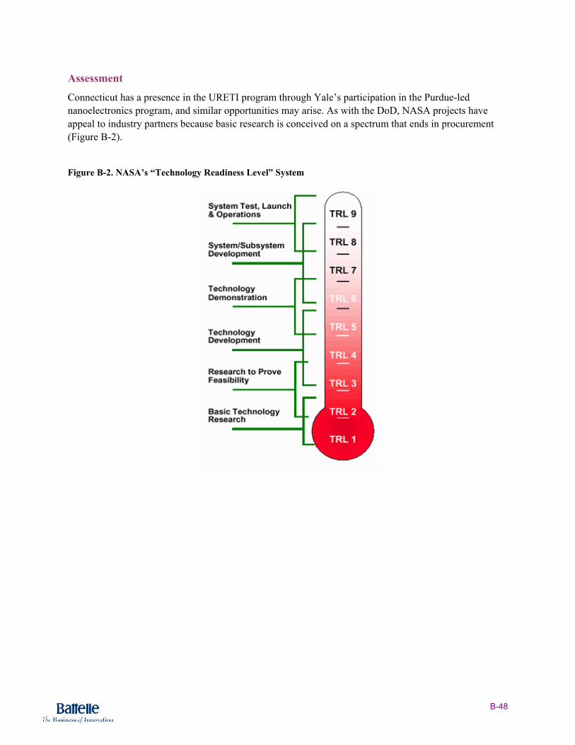
B-48
Assessment
Connecticut has a presence in the URETI program through Yale’s participation in the Purdue-led nanoelectronics program, and similar opportunities may arise. As with the DoD, NASA projects have appeal to industry partners because basic research is conceived on a spectrum that ends in procurement (Figure B-2).
Figure B-2. NASA’s “Technology Readiness Level” System

B-49
DEPARTMENT OF AGRICULTURE ($11 MILLION)
Nanotechnology Interests
USDA lists interest in three PCAs: nanomaterials, nanoscale devices and systems, and societal dimensions. Unspecified projects classified as NNI-related exist at both the intramural Agricultural Research Service64 (a funding sink, not a source, and in any case not represented in Connecticut) and the extramural Cooperative State Research, Education, and Extension Service (CSREES).65
Current Opportunities
No USDA program solicitations are aimed exclusively at nanotechnology, but proposals can be addressed to opportunities found at http://www.csrees.usda.gov/fo/funding.cfm. SBIR opportunities are at http://www.csrees.usda.gov/funding/sbir/sbir_highlights.html.
NSET Representative
Dr. Hongda Chen, National Program Leader for Bioprocess Engineering, CSREES, (202) 401-6497. [email protected].
Assessment
USDA-CSREES should be disregarded in strategy formation, although it is a potential source of funding for specific investigators and programs. Connecticut has two agricultural experiment stations co-funded by the state and CSREES.66 While much of the academic research at experiment stations is pre-programmed by station directors according to formula distributions, agricultural researchers are encouraged to apply for competitive awards from other units of CSREES and other federal agencies. This could be a minor opportunity.
64 See http://www.ars.usda.gov/main/main.htm. 65 See http://www.csrees.usda.gov/. 66 The independent Connecticut Agricultural Experiment Station at New Haven and the Storrs Agricultural Experiment Station, the research arm of UCONN’s College of Agriculture and Natural Resources.

B-50
ENVIRONMENTAL PROTECTION AGENCY ($5 MILLION)
Nanotechnology Interests
The Environmental Protection Agency (EPA) is interested in four PCAs: nanomaterials, nanoscale devices and systems, nanomanufacturing, and especially societal dimensions—where it is one of only two federal agencies (the other being HHS) strongly interested in health effects as they relate to the “responsible use” mandate. Grant-making rests largely with the National Center for Environmental Research (NCER),67 the extramural research-funding arm of the EPA Office of Research and Development (ORD).68 The balance of ORD’s laboratories are largely intramural funding “sinks,” although there are some competitive funds available. It seems unlikely that intramural programs are absorbing large amounts of NNI funding, because they operate at a fairly applied stage of development. Therefore, we assume that most of the $5 million budgeted for NNI is probably available through various competitive opportunities from NCER.
Existing Centers
EPA NCER has not sponsored large-scale centers, but last fall announced 12 exploratory research awards69 (mid-six figures each) on the environmental impacts of nanotechnology through its Science to Achieve Results Program. Universities with investigators receiving funding were the University of Utah, UC-SB, NCSU, University of Rochester, Arizona State University, University of South Carolina at Columbia, Brown, Iowa, Rice, University of California at Davis, Delaware, and Purdue. The overlap with universities that had already made substantial infrastructure investments and/or attracted NSF funding is clear.
Current Opportunities
No EPA program solicitations are aimed exclusively at nanotechnology, but proposals can be addressed to opportunities found at http://es.epa.gov/ncer/rfa/. More broadly, ORD opportunities are at http://www.epa.gov/ord/htm/grantopportunity.htm and agency-wide opportunities at http://www.epa.gov/etop/. SBIR opportunities can be found at http://es.epa.gov/ncer/sbir/.
NSET Representatives
• Dr. Barbara Karn, Environmental Scientist, NCER, ORD, (202) 564-6824. [email protected].
• Dr. Stephen Lingle, Director, Environmental Engineering Research Division, NCER, ORD, (202) 343-9699. [email protected].
• Dr. Nora Savage, Environmental Engineer and SBIR Program Specialist, NCER, ORD, (202) 343-9858. [email protected].
• Dr. Philip Sayre, EPA Science Advisory Board Staff Office, (202) 564-7673. [email protected].
67 See http://es.epa.gov/ncer/. 68 See http://www.epa.gov/ord/htm/orgchart.htm. 69 See http://cfpub.epa.gov/ncer_abstracts/index.cfm/fuseaction/recipients.display/rfa_id/352.

B-51
Assessment
EPA is probably at the lower threshold of agencies that should be considered in strategy formation. Its budget for NNI is small, but its interest in societal dimensions and health effects may be significant for Connecticut given potential synergies with NIH-funded research. Moreover, while several states and institutions have begun early with programs and centers studying environmental impacts, it is fair to say that no single one has established a dominant position of national leadership. This could be an opportunity, albeit of modest size. Finally, there is strategic importance to any R&D embedded in a regulatory agency: technologies that meet regulatory standards because they were developed in partnership with the regulatory agency often find built-in markets both in government and the private sector.

B-52
DEPARTMENT OF JUSTICE ($2 MILLION)
Nanotechnology Interests
The Department of Justice’s (DoJ’s) nanotechnology interest focuses exclusively on the nanoscale devices and system PCA. Specifically, the Office of Science and Technology of the National Institute of Justice70 is developing two classes of devices that are assumed to benefit from nanotechnology research: (1) DNA analysis for forensics and (2) warning device for chemical and biological hazards.
Current Opportunities
No DoJ program solicitations are aimed exclusively at nanotechnology, but applications-oriented research proposals can be addressed to opportunities listed at http://www.ojp.usdoj.gov/nij/funding.htm#cs.
NSET Representative
Stanley Erickson, Chief, Research and Technology Division, Office of Science and Technology, National Institute of Justice, (202) 305-4686.
Assessment
DoJ’s research unit is highly applications-focused, and its nanotechnology interests are small even in the context of a modest-sized R&D program. The nature of the linkage between the R&D program and federal or state purchasing power is as yet undefined. Therefore, DoJ can be disregarded in strategy formation, although it is a potential source of funding for specific investigators.
70 See http://www.ojp.usdoj.gov/nij/sciencetech/welcome.html.
B-53
DEPARTMENT OF HOMELAND SECURITY ($1 MILLION)
Nanotechnology Interests
DHS has interest in three PCAs: fundamental nanoscale phenomena; nanoscale systems and devices; and instrumentation research, metrology, and standards. DHS considers nanotechnology important mainly for developing explosives-detection technology for use in transportation security. These interests rest within the DHS Science and Technology Organization,71 which comprises both an intramural Office of Research and Development72 and an extramural Homeland Security Advanced Research Projects Agency73 that includes the Department’s university centers and SBIR programs.
Current Opportunities
There are no DHS program solicitations aimed exclusively at nanotechnology, but proposals can be addressed to occasional BAAs and other opportunities found at http://www.dhs.gov/dhspublic/display?theme=37&content=3608. SBIR opportunities can be found at http://www.hsarpasbir.com/.
NSET Representatives
• Richard Lareau, Transportation Security Research and Development Division, William J. Hughes Federal Aviation Administration Technical Center, Transportation Security Administration, (609) 485-4877. [email protected].
• Keith Ward, Program Manager, Homeland Security Advanced Research Projects Agency, (202) 205-1535. [email protected].
Assessment
DHS may be of significant importance to Connecticut due to the presence of the Coast Guard R&D Center74 at Groton. While this Center offers no known extramural funding opportunities, its presence may provide an opportunity to help shape what will certainly be a rapidly growing R&D program within DHS. Every effort should be made to establish contacts with DHS, at Groton, at the NSET representative level, and at higher levels in the Science and Technology Organization. In the indefinite future, it is very likely that technologies developed through the DHS R&D program may address major markets through direct federal and state/local purchasing, subsidized by federal grant programs.
71 See http://www.dhs.gov/dhspublic/interapp/editorial/editorial_0531.xml. 72 See http://www.dhs.gov/dhspublic/interapp/editorial/editorial_0533.xml. 73 See http://www.dhs.gov/dhspublic/interapp/editorial/editorial_0534.xml. 74 See http://www.rdc.uscg.gov/. For contacts see http://www.rdc.uscg.gov/rdcpages/Contact-Us.html.

B-54

C-55
Appendix C. Benchmarking Case Studies and Best Practice Lessons
BENCHMARKING INTRODUCTION Following is a summary of lessons learned from a benchmarking exercise in which Battelle examined the status of nanotechnology initiatives in three other states—Massachusetts, New York, and Pennsylvania in the northeastern region. This appendix includes full profiles of each of these three states and vignettes of other activities around the nation.
SUMMARY BY GEOGRAPHY • Clusters of expertise have arisen without government intervention at nearly every major research
institution in Massachusetts, with a strength in polymers in several of these (especially the Massachusetts Institute of Technology [MIT] and the University of Massachusetts [UMass} at Amherst). Even Harvard, where the chemistry department has made seminal contributions to the science that underlies nanotechnology, has started to make significant new investments in facilities that allowed it to capture new federal funding. However, some of the strongest industrial participation is in traditional microelectronics programs at MIT that have migrated steadily toward the nanoscale. Formation of spin-offs has been well distributed across the eastern portion of the state. In its recent decision to support the National Science Foundation (NSF)-sponsored Nanoscale Science and Engineering Center (NSEC) captured by Northeastern and UMass-Lowell, the state has declared an interest in nanomanufacturing as a way of revitalizing the Merrimack Valley.
• Nanotechnology in New York State has developed top-down, both as part of the state’s strategy to address the needs of the microelectronics sector and through existing interdisciplinary collaborations at Cornell and Columbia. The top-down strategy builds on years of investment by the state in the academic/industrial collaborations at a range of institutions. Ultimately, the state picked the State University of New York at Albany (SUNY Albany) as the receptacle for a major investment timed to influence International Business Machines Corporation’s (IBM’s) decision on locating its next-generation fabrication facility. Meanwhile, building on programs that until recently enjoyed little state support, both Cornell and Columbia have attracted significant new federal funding, and the former is developing a nanobiotechnology specialization with two nanotechnology spin-offs to its credit.
• Responding to a locally developed initiative, Pennsylvania invested decisively in the Nanotechnology Institute, a collaborative activity that makes Southeastern Pennsylvania the clear leader in bionanotechnology, despite much earlier and deeper investment in the central portion of the state. This Institute already has a good track record at attracting funding from large companies and in stimulating spin-off formation. Moreover, alliances formed through the Institute gave the region early visibility in Washington and allowed the University of Pennsylvania (Penn) to attract the state’s first NSEC.

C-56
SUMMARY Following is a summary of principal lessons learned, drawing on the three detailed profiles and other instances around the nation as relevant.
Building on Prior Strengths and Making Upfront Investments are Important
Leading centers of nanotechnology reflect significant upfront investments that either leverage existing strengths or in some circumstances create new capacity. Table C-1 summarizes the prior strengths on which major nanotechnology initiatives have been built in each of the three benchmark states and also California. Some of these foundational strengths emerged organically from long-standing commitments to interdisciplinary science. For example, Drexel University and Penn in the 1990s each focused on building expertise in bioengineering and biomaterials, which was then leveraged by the state-funded Nanotechnology Institute. In turn, this enabled the region to capture an NSF NSEC on the bio/nanotechnology interface. Northeastern University used a $2 million alumni donation to extend that existing microelectronics expertise with nanolithography and associated instrumentation. Together with state support for similar efforts at UMass-Lowell, this led directly to capture a new NSF NSEC in High-Rate Nanomanufacturing. At SUNY Albany, a steady stream of state support for thin-film technology during the 1990s had cumulated to $200 million (and a cluster of state-, federal-, and industry-sponsored programs) before the Albany Nanotech initiative was launched as the cornerstone to recruitment of International Sematech North.
Table C-1. Results of Upfront Nanotechnology Investments in Massachusetts, New York, Pennsylvania, and California
State Institution Building Block Center Resultant Impact MIT NSF Materials Research Science and
Engineering Center (MRSEC) Continued development in polymer nanostructures
MIT Microsystems Technology Laboratory Evolved into Nanostructures Laboratory Northeastern NSF Industry/University Cooperative
Research Center (I/U CRC) in Microcontamination
NSF NSEC in Nanomanufacturing with Lowell
Harvard Center for Imaging and Mesoscale Structures (NSF) National Nanotechnology Infrastructure Network (NNIN)
NSF NSEC in Science of Nanoscale Systems and Device Applications
UMass-Amherst NSF I/U CRC in polymers, nanostructures group NSF MRSEC, aqueous assembly group
System-funded MassNanoTech Partners consortium
Massachusetts
Boston University (BU)
Photonics Center Center for Nanoscience and Nanobiotechnology
New York SUNY Albany
New York State Office of Science, Technology, and Academic Research (NYSTAR) Center for Advanced Technology (CAT) for Thin Films; Semiconductor Research Corporation (SRC) Interconnect Focus Research Center
Albany Nanotech/International Sematech North and associated activities

C-57
State Institution Building Block Center Resultant Impact
Cornell NSF NNIN Nanoscale Science and Technology Facility NSF MRSEC, nanoscale research group
NSF NSEC in Nanoscale Systems for Information Technology NSF Science and Technology Center on Nanobiotechnology Kavli Institute for Nanoscale Science
Columbia Center for Integrated Science and Engineering NSF MRSEC
NSF MRSEC reinvented at renewal as Center for Nanostructured Materials NSF NSEC shared with Cornell for Electron Transport in Molecular Nanostructures NSF/the U.S. Department of Energy (DOE) Institute for Environmental Molecular Science
New York (cont.)
Rensselaer Polytechnic Institute (RPI)
NYSTAR CAT for Automation Technology
NSF NSEC for Directed Assembly of Nanostructures Nanotechnology component of Center for Biotechnology and Interdisciplinary Studies
Penn NSF MRSEC – Laboratory for Research on Structure of Matter and facilities for interaction with medical school
Nanotechnology Institute with Drexel and NSF NSEC on Nano/Biotechnology Interface
Pennsylvania
Drexel School of Biomedical Engineering See above California University of
California, Santa Barbara (UCSB)/University of California, Los Angeles (UCLA)
California Nanotechnology Systems Institute (CNSI)
Defense Advanced Research Projects Agency (DARPA)/Department of Defense (DoD) Center for Nanoscience Innovation in Defense NSF NSEC in Scalable and Integrated Nanomanufacturing at UCLA Army Institute for Collaborative Biotechnologies with MIT
State Matching Funds are Critical
Existing or naturally evolved capacity is often not sufficient to attract a major federally sponsored research center. Provision of state matching funds, even if not a formal legal requirement, often improves the odds of a proposal’s acceptance. This is true even for leading universities like Cornell, which had state support to win two new federal centers in nanotechnology in addition to its long-established user facility. For example, the state made a separate $2.8 million grant for an Alliance for Nanomedical Technology as a bridge between the existing nanotechnology activities and a separate cluster of bioscience initiatives. Similarly, UMass-Lowell, which is known mainly for its strength in polymer processing and not widely considered a top-tier nanotechnology center, initially failed in its attempt to attract a federal nanotechnology center in conjunction with Northeastern, but then succeeded with a $5 million state match and a committed $21 million for facility construction. In fact, provision of facilities is a very important way that states can show their commitment to pending federal proposals (see Table C-2).

C-58
Table C-2. Matching Funds and Contributions for Facility Construction for Selected States
State Direct Match to Federal Award Capital Contribution Other
Massachusetts $5M to NSEC on nanomanufacturing (Northeastern/Lowell)
$21M earmarked for construction of center headquarters at Lowell
$200K in UMass budget to seed industry/university consortium at Amherst
New York Unspecified match to NSF NSEC at Cornell in nanoelectronics, photonics, magnetics $300K in direct matching and $2.8M in collateral Nanomedical center to attract NSF Science and Technology Center in nanobiotechnology to Cornell
$50M+ invested in new 300-millimeter wafer fabrication capacity at SUNY Albany, on top of $200M existing microscale investments
$150M in incentives to IBM to keep 300-millimeter fabrication local $250M state-led redevelopment of office campus as R&D park Misc. faculty development awards to attract stars
Pennsylvania $14M in cumulative (unrestricted) support to Nanotechnology Institute helped leverage NSF NSEC on bio/nanotechnology interface at Penn
Unspecified investment over years in Penn State Materials Institute, both on campus and in the research park
$3.5M to NNIN user facility at Penn State to establish commercialization capability $1.2M investment in nanotechnology spin-off of Penn State through Central PA Life Sciences Greenhouse (tobacco settlement funded)
California $100M commitment to CNSI facilities at UCLA and UCSB, levering $150M in federal awards
Note: ongoing funding often available through UC Discovery Grant, Micro category
Illinois $17M to $23M to match DOE support for Center for Nanoscale Materials at Argonne $5M toward Northwestern’s new center, levering NSF NSEC in transportation applications $18M through the University of Illinois (UI) system budget for new facilities at UI at Urbana-Champaign (UIUC), leveraging NSF NSEC in nanomanufacturing
Indiana Initial $1.5M grant to Purdue with potential for $30M over 10 years from 21st Century Fund leverages two centers at Purdue, National Aeronautics and Space Administration (NASA) in nanoelectronics and NSF in nanocomputation
$5M in “Energize Indiana” funds from securitizing tobacco settlement toward Birck Nanotechnology Center at Purdue Discovery Park
New Jersey $2M from NJ Science and Technology Commission to convert Lucent wafer fabrication into nanotechnology user facility open to academia/industry

C-59
State Direct Match to
Federal Award Capital Contribution Other
Ohio $2M capital grant from Third Frontier Wright Centers program leveraged NSF NSEC in polymer nanomaterials at the Ohio State University. Additionally funding from the Wright Centers program will provide $22.5 million to establish a multi-institutional polymer nanotechnology center (including new equipment).
Oregon $20M in line item for capital costs and $1M in operating for consortial nanoscience institute across Oregon State University (OSU), the University of Oregon (UO), and Oregon Health and Science University (OHSU), leveraging industry support
State Funds Can Activate Industry Linkages Through Intermediary Organizations
In many of the cases cited above, state funding has been invested in not only university research capacity but creation of intermediaries that facilitate industrial collaboration. In Philadelphia, the Nanotechnology Institute was specifically designed as an academic/industrial consortium involving firms that financially support the effort and in turn receive early access to negotiate licenses to research discoveries. Companies involved in this consortium include a broad range of bioscience companies active the region, including Merck, GlaxoSmithKline, Cephalon, and Elan. The situation in Albany is extreme in the sense that state investment in the facility was as much a business-development project as an effort to build university research. Albany Nanotech was conceived as an academic testbed to encourage close industry collaboration as wafer lithographic technology migrates from the microscale to the nanoscale over the next 10 to 15 years. With $150 million in bonding incentives from New York State, IBM did commit $1.9 billion to building its 300-millimeter wafer facility in nearby Fishkill, along with development partners Sony, Toshiba, Samsung, Infineon, AMD, and Charter. In other cases, intermediaries are created as stewards of user facilities. Table C-3 summarizes other examples, either university-based or independent nonprofit.
Table C-3. Intermediaries, Their State Support and Industry Members, for Selected States
State Intermediaries State Support? Industry Members
Mass NanoTechPartners will be built on an affiliates model Y TBD
Northeastern/Lowell NSEC in Nanomanufacturing Y
Wolfe, Foster-Miller, Rosseter, Motorola, TSI, Zyvex, ADL, SC Fluids, Draper, Environ, Tyco, M/A Com, Konarka
Massachusetts
UMass-Amherst Center for UMass-Industry Research on Polymers (CUMIRP) nanostructures interest group
Y (historical)
DuPont, Kodak, Essilor, General Electric (GE), Solutia, U.S. Army

C-60
State Intermediaries State Support? Industry Members
MIT Nanostructures Lab N
AMD, Analog, Applied Materials, Hewlett Packard/Compaq, IBM, Intel, Lucent, Motorola, National Semi, Novellus, Taiwan Semi, TI
MIT Institute of Soldier Nanotechnology N Raytheon, DuPont, Partners Healthcare International Sematech North at SUNY Albany is the private-sector partner for Albany Nanotech
Y Sematech becomes the vehicle for attracting inward investment (TEL, Applied Materials, ASML)
IBM Y Development partners Sony, Toshiba, Samsung, Infineon, AMD, Charter
New York
Cornell Alliance for Nanomedical Technologies Y
29 companies, including start-ups, mid-sized New York State companies, and large firms with headquarters (Corning; Moog, Welch Allyn, etc.)
Pennsylvania Nanotechnology Institute, a collaboration of nine universities, one hospital, and industry partners
Y Merck, GlaxoSmithKline, Elan, Cephalon, etc.
California CNSI Y Applied Materials, Hewlett Packard, Intel, Sputtered Films, SUN, Veeco, etc.
New Jersey NJ Nanotechnology Consortium is operated by Lucent as an open user facility welcoming academic and corporate users
Y
Oregon Oregon Nanoscience and Microtechnologies Institute is on the same general model as NJ but distributed across several universities
Y Hewlett Packard, FEI, Pixelworks, Planar, Intel, LSI, Battelle, and others
Texas Strategic Partnership for Research in Nanotechnology links centers at Austin, Houston, and Dallas/Richardson
N Nanotechnology Foundation of Texas funnels charitable contributions in lieu of direct state support
Virginia Virginia Nanotechnology initiative set up by Center for Innovative Technology (CIT) functions as an intermediary.
Y
Universities Also Need to Collaborate
Few universities are able to stand alone as nanotechnology centers of excellence, especially since the NSF has learned to favor inter-institutional collaboration. Even Harvard and MIT have joined forces, along with several others, in winning the NSF NSEC for Nanoscale Systems and Device Applications. Other consortia include Drexel/Penn, UMass-Lowell/Northeastern/University of New Hampshire (UNH); and, of course, UCSB/UCLA.
Nanotechnology Education and Training Are Complementary but Lagging
Despite the growing base of nanotechnology research and centers of excellence, it is still not clear how nanotechnology will be introduced in education and training. Nanotechnology grows of the interaction of chemistry, physics, materials science, engineering, and biology. Education programs may be integrated into the curricula of these established disciplines rather than developed into stand-alone degree programs. One exception to date is SUNY Albany—a university without an engineering school that now has a College of Nanoscience and Engineering (graduate-level only) as part of the state investment that recruited International Sematech. Clearly, education and training are being offered at universities with

C-61
research centers, which are actively connecting with community and technical colleges to ensure a trained workforce. For example, Penn State has established a Center for Nanotechnology Education and Utilization that works with an associated educational consortium to provide skills for management of nanotechnology fabrication facilities. Also, the Nanotechnology Institute in Philadelphia was active in developing a community college curriculum with Department of Education support. In Texas, a new workforce initiative was announced at Texas State Technical College in conjunction with Zyvex, the molecular self-assembly company in Richardson, in the Telecom Corridor.

C-62
C-63
Massachusetts
SUMMARY University-based nanotechnology research and commercialization activity in Massachusetts has a strength in manufacturing:
• At MIT, where nanotechnology had once been of interest only to microelectronics and optics experts, the situation changed almost overnight in 2002 when the university marshaled its diverse strengths in materials science and manufacturing to win a huge, $50 million Defense Department contract to use nanotechnology to develop a new generation of lightweight, high-strength materials to better protect soldiers in combat. Contractors who sell actual products to the Defense Department are participating as co-funders.
• The early success of Konarka, a UMass-Lowell nanotechnology spin-off developing flexible solar cells, encouraged policymakers to view nanotechnology as the route to a revival of manufacturing in the Merrimack Valley, once a center of textile production. State support enabled Lowell to join with Northeastern University (an expert in microelectronics process contamination) in winning a major NSF NSEC focused specifically on high-volume nanomanufacturing. A significant number of major companies are partnering.
• Harvard, where the chemistry department has underpinned many fundamental advances in nanotechnology, but which does not have an otherwise strong reputation in spin-off formation, has produced at least two “platform” companies specializing in inorganic applications of nanotubes.
• Meanwhile, nanobiotechnology applications are becoming a strong focus at MIT, which is sharing another large Defense Department award with UCSB and the California Institute of Technology (Caltech), at BU; and at the Center for Integration of Medicine and Innovative Technology (CIMIT),75 the consortium for medical technology development that involves MIT, Harvard Medical School, Partners Healthcare, and the Charles Stark Draper Laboratory.
• Belatedly, the state is acknowledging an existing nanotechnology expertise at UMass-Amherst by creating an industry consortium separate from the polymer center from which faculty expertise emerged.
BACKGROUND ON MASSACHUSETTS SCIENCE AND TECHNOLOGY PROGRAMS Until recently, Massachusetts state government has rarely made funding available to develop university-based research capability, in part because science and engineering strength at MIT and Harvard runs so broad and deep. However, in synch with an extensive roadmapping exercise commissioned by the nonpartisan policy group Mass Insight,76 the state two years ago passed a $100 million economic stimulus package that includes $35 million in direct support for science and technology research in support of economic development.
75 See http://www.cimit.org/about_ov.html. 76 See http://www.massinsight.com/.

C-64
This support flows through the Massachusetts Technology Collaborative,77 a quasi-public corporation originally created in the 1980s to develop a microelectronics research park, but subsequently used to promote the formation of technology clusters. The stimulus package gave the Collaborative responsibility for two programs: a $20 million fund called the John Adams Innovation Institute and a $15 million fund for regional technology projects. The John Adams Innovation Institute provided $5 million in committed state matching support for an NSF NSEC (see below). No other awards from the John Adams Innovation Institute or the regional program have yet been announced.
Massachusetts has been somewhat more aggressive in making investment funding available for early-stage ventures. Among the sources are as follows:
• The Massachusetts Technology Development Corporation (MTDC),78 another quasi-public corporation that operates a seed fund and invests in a later-stage fund. At present, MTDC seems to have no nanotechnology in its portfolio.
• The Massachusetts Renewable Energy Trust, another program of the Collaborative, which offers direct seed investments of $50,000 to $500,00079 and invests as a limited partner with Commons Capital80 of Brookline in a Green Energy Fund.
The UMass system itself, which maintains an Office for Economic Development, has recently revitalized the Commercial Ventures and Intellectual Property Office, equipping it with both a fund for commercialization research and a new Center for Technology Transfer charged with forming industry partnerships.81
MASSACHUSETTS INSTITUTE OF TECHNOLOGY MIT has long-standing interests in nanotechnology through several interrelated programs, all of which draw heavily on the university’s Industrial Liaison Program:82
• An NSF-sponsored MRSEC83 founded in 1994 and continued in 2002, with a long-standing research group on polymer nanostructures.
• The Nanostructures Laboratory84 (formerly the Microsystems Technology Laboratory). This consortium of user facilities has roots at MIT dating to the 1970s. These labs focus on fabrication, characterization, and metrology relevant to short-channel semiconductors, nanophotonics, and nanomagnetics. Its industry partners include Advanced Micro Devices, Analog Devices, Applied Materials, Hewlett Packard/Compaq, IBM, Intel, Lucent, Motorola, National Semiconductor, Novellus, Taiwan Semiconductor, and TI.
• The Space Nanotechnology Laboratory,85 a NASA-supported facility within the Center for Space Research that dates to 1993. Its specific focus is on interference lithography to create gratings for the
77 See http://www.mtpc.org/. 78 See http://www.mtdc.com/index.html. 79 See http://www.mtpc.org/seed/index.htm. 80 See http://www.commonscapital.com/index.htm. 81 See http://www.cvip-umass.net/index.cfm?fuseaction=generic.3. 82 See http://ilp-www.mit.edu/display_page.a4d?key=H1. 83 See http://web.mit.edu/cmse/www/. 84 See http://nanoweb.mit.edu/. 85 See http://snl.mit.edu/history.html.

C-65
Chandra Space Telescope. Its current focus is a nanoruler with 3-nanometer feature resolution. The main sponsor is NASA, with additional support from DARPA, Los Alamos, Southwest Research Institute, and the NSF.
Levering this expertise, MIT successfully competed in 2002 for the Institute for Soldier Nanotechnologies at MIT;86 a five-year, $50 million contract from the U.S. Army Research Office (Durham). The Institute is aimed specifically at developing technology for improving the survival of soldiers. Seven teams focus on energy absorbing materials; mechanically active materials and devices; sensing and counteraction; biomaterials and nanodevices for medical technology; processing and characterization (nanofoundries); modeling and simulation of materials and processes; and systems design, hardening, and integration. The founding industry partners are Raytheon, DuPont, and Partners Healthcare. In all, industry sponsors are directing $22 million in parallel contracts to the Institute.
Subsequently, MIT also shared a separate, $50 million grant from the Army Research Office for an Institute for Collaborative Biotechnologies87 that will have nanotechnology components. MIT’s partners in this initiative are UCSB and Caltech.
MIT does not regularly update information on its portfolio of start-up companies, but the following start-up companies clearly have MIT roots:
• Angstrom Medica,88 a biomaterials licensee founded by a former MIT graduate student
• Nano-C,89 a licensee manufacturing high-purity fullerenes, founded by an MIT Emeritus Professor.
MIT also has a privately endowed Deshpande Center for Technological Innovation,90 which has seed funds available to help assemble business plans around the work of MIT researchers. More deals with nanotechnology content are anticipated.
NORTHEASTERN AND THE UNIVERSITY OF MASSACHUSETTS–LOWELL The Center for High-Rate Nanomanufacturing91 is an NSF-sponsored NSEC headquartered at Northeastern University ($4.7 million), but with nearly equal participation from UMass-Lowell ($3.4 million) and the UNH ($3.3 million) and smaller roles for Michigan State University and the Boston Museum of Science. The state’s matching support from the John Adams Innovation Institute will flow through the Lowell campus (see below). The main focus of the Center is developing, testing, and evaluating “templates” for guided self-assembly of nanostructures.
Northeastern
Northeastern contributes to the Center microelectronics expertise developed during the last several years through its NSF-sponsored Industry/University Center for Microcontamination Control.92 Prior to announcement of the NSEC award, Northeastern had received a $2 million donation from alumnus
86 See http://www.web.mit.edu/isn/aboutisn/index.html. 87 See http://web.mit.edu/newsoffice/2003/icb.html. 88 See http://www.angstrommedica.com/aboutus/default.htm. 89 See http://www.nano-c.com/. 90 See http://web.mit.edu/deshpandecenter/. 91 See http://www.nano.neu.edu/aboutus.html. 92 See http://www.cmc.neu.edu/.
C-66
George Kostas to create a Nanoscale Technology and Manufacturing Center Facility93 as an extension to the existing Microfabrication and Microcontamination Laboratory in the Egan Research Center. The extension includes Class 100 and Class 10 clean room capability for nanolithography and associated instrumentation. Northeastern also has associated initiatives in nanomedicine and nanomaterials.94
University of Massachusetts–Lowell
Lowell, a modest branch of the UMass system with a strong culture of industry collaboration, is contributing to the Center its expertise on polymers. Lowell will be the focal point for the $5 million matching contribution from the John Adams Innovation Institute, in the form of a Center of Excellence in Nanomanufacturing. This allocation will be used primarily to seed industry collaborations for the NSEC (see below). The governor’s FY06 budget also includes a $21 million earmark for construction of a headquarters for the Center in the Lawrence Mills brownfield redevelopment area. Lowell believes it also has a role to play in the environmental impacts facet of the National Nanotechnology Initiative because of its School of Health and Environment.
In 2001, Lowell spun off Konarka Technologies,95 the state’s best-known nanotechnology startup. Based in a nearby converted textile mill, Konarka has raised $35 million in venture capital—including seed amounts from the Massachusetts Renewable Energy Trust—for its program of placing nanoscale photovoltaic cells on flexible substrates.
Summary of Industrial Involvement
The NSEC claims $9 million in industrial support from partners such as Wolfe Laboratories, Foster-Miller, Rosseter Holdings, Motorola, TSI, Zyvex, AD Little, SC Fluids, Draper, Environ, Tyco, M/A Com, and Konarka.
HARVARD Harvard has long hosted an NSF-sponsored Materials Science and Engineering Center,96 but it is not one of the MRSECs with a strong nanotechnology focus. Rather, members of Harvard’s Chemistry Department (including Profs. Lieber, Whitesides, and others) have contributed substantially to the development of nanotechnology. Starting in 1999, the university recognized this emerging strength as part of its $200 million commitment to new interdisciplinary research centers. The core of the nanotech effort was the Center for Imaging and Mescoscale Structures (CIMS),97 a user facility that soon became a node on the NSF National Nanofabrication User Network.
CIMS focuses on soft lithography, assembly of nanoscale molecular electronics, simulation of electron states and transport, and building the necessary computational resources. This commitment helped Harvard capture lead role in the NSF-funded Center for the Science of Nanoscale Systems and Device Applications,98 funded at $10.8 million over five years. (The other partners in this NSEC are MIT, UCSB, and the Museum of Science in Boston.) The focal areas of this Center are novel electronic and
93 See http://www.nano.neu.edu/facilities.html. 94 See http://www.nanotech.neu.edu/index.htm. 95 See http://www.konarkatech.com/about/history_of_konarka.php. 96 See http://www.mrsec.harvard.edu/. 97 See http://cims.harvard.edu/about/origins.html. 98 See http://www.nsec.harvard.edu/nsecsumm.htm.

C-67
magnetic devices, synthesis and growth of nanomaterials, imaging of electrons, and study of spins and charges. Both the CIMS and NSEC will be housed in a newly constructed Laboratory for Integrated Science and Engineering..99
Start-up nanotechnology companies with Harvard chemistry affiliations include the following:
• Nanosys,100 an inorganic nanotechnology platform company co-founded by a faculty member
• Nantero,101 a developer of carbon nanotubes for semiconductor applications, founded by several departmental alumni.
UNIVERSITY OF MASSACHUSETTS–AMHERST At the main campus at UMass-Amherst, nanotech R&D has evolved as a consequence of the campus’s long-standing core competency in polymer science. The NSF-sponsored MRSEC in Polymers has long had a specialty in aqueous polymer assembly, integrating nanoparticles with block copolymers.102 Investigators in this interdisciplinary group are seeking to develop methods of fabricating nanoscale membranes, sensors, controlled-release devices, and biocompatible materials. Some of the same faculty are also involved in the NSF-sponsored I/U CRC on Polymers. One of six research clusters focuses on functional nanostructured materials,103 with dues-paying industrial participation from DuPont, Kodak, Essilor, GE, Solutia, and the U.S. Army, which also recognizes the campus as a Polymer Center of Excellence. In pursuing these areas, the nanopolymer programs benefit from the opening in 1996 of a six-story, 176,000-square-foot laboratory building for polymer science constructed at a cost of $56 million in combined university and federal line-item support. Included in this new building is a separate W M. Keck Foundation Nanostructures Laboratory,104 a user facility for characterization at the nanoscale.
In 2004 the UMass system allocated $200,000 to seed MassNanoTech Partners,105 an industry collaborative inspired by the polymer I/U CRC. Originally intended to link faculty at Amherst with those at Lowell and Worcester, the initiative became more focused on Amherst itself once the state had agreed to support the Lowell/Northeastern High-Rate Nanomanufacturing Center. The initiative provides easy industrial access to as many as 50 investigators from eight departments. Industrial partners are invited to join as many as they wish of three “technical research groups”: nanoscale materials and processes, nanoscale electronic devices, and bionanotechnology. Dues vary from $12,000 for a small company to $36,000 for a large one, with discounts for each additional group joined. At about the same time this initiative was launched, UMass-Amherst recruited a new faculty member with expertise at the nanoscale, Dr. Kenneth Carter of the IBM Almaden Research Center.
99 See http://www.nsec.harvard.edu/nugget_1_lise.htm or http://construction.fas.harvard.edu/projects/lise/. 100 See http://www.nanosysinc.com/about/history.html. 101 See http://www.nantero.com/fteam.html. 102 See http://www.pse.umass.edu/mrsec/irgs3.html. 103 See http://www.pse.umass.edu/cumirp/pdf/clustern.pdf. 104 See http://www.pse.umass.edu/nano/. 105 See http://www.umass.edu/massnanotech/partner.htm.

C-68
OTHER • Boston College is the source of intellectual property for NanoLab,106 a four-year-old nanotubes
vendor co-founded by two physics professors.
• BU has created a Center for Nanoscience and Nanobiotechnology107 to connect photonics research at the Charles River campus with biomedical capability at the BU Medical Campus. The Center’s industrial liaison program anticipates six to ten members within three years, at membership tiers ranging from $5,000 to $250,000. As part of this effort, the BU Photonics Center has added a $1.5 million Nanophotonics Lab with 1,000 square feet of Class 100 clean room workstations. The center also intends to collaborate with the Brookline-based Fraunhofer Center for Manufacturing Innovation.108
SUMMARY Clusters of expertise have arisen without government intervention at nearly every major research institution in Massachusetts, with a strength in polymers in several of these (especially MIT and UMass-Amherst). Even Harvard, where the chemistry department has made seminal contributions to the science that underlies nanotechnology, has started to make significant new investments in facilities that allowed it to capture new federal funding and would certainly play a role if the university decides to add engineering programs at its Allston (business school) campus. However, some of the strongest industrial participation is in traditional microelectronics programs at MIT that have migrated steadily toward the nanoscale. Formation of spin-offs has been well distributed across the eastern portion of the state. In its recent decision to support the NSF-sponsored NSEC captured by Northeastern and UMass-Lowell, the state has declared an interest in nanomanufacturing as a way of revitalizing the Merrimack Valley.
106 See http://www.nano-lab.com/team.html. 107 See http://nanoscience.bu.edu/about.htm. 108 See http://www.fhcmi.org/industries_files/industries.html.

C-69
New York
SUMMARY University nanotechnology research and commercialization activity in the State of New York divides into several broad categories:
• Huge state investments in migrating existing microelectronics and thin-film capability at SUNY Albany to the nanoscale, conceived as a program for industrial retention (IBM’s 300-millimeter wafer fabrication facility at Fishkill) and attraction (Sematech, Tokyo Electron, Applied Materials, ASML, and others).
• More modest state matching of long-standing, federally funded materials-science infrastructure at Cornell University, which led naturally to federal funding of a nanobiotechnology focus that fits well with the university’s major life science initiative and has led to both industry partnerships and spin-off formation at Ithaca.
• Strong, but essentially self-generated initiatives at Columbia University and RPI, which leverage small amounts of state support but more importantly reflect NSF’s appreciations of both institutions’ commitments to interdisciplinary science and engineering research.
• Marketing and packaging of every nanotechnology-related development statewide on a NanoNY109 Web site maintained by the state science and technology agency. This site includes links to centers,110 weekly news briefs, white papers, and notices of patents obtained and licensing opportunities. This packaging gives a coordinated feel to what is actually a highly decentralized nanotechnology effort.
BACKGROUND ON NEW YORK STATE’S SCIENCE AND TECHNOLOGY PROGRAMS Each of the major universities in New York State, both public and private, participates in some way in programs for academic/industrial collaboration offered by the state.
The first program to develop was the CAT111 program offered by NYSTAR.112 Each CAT is funded at $1 million annually for operations and programs and must match that amount with cash or contributions from New York State companies. In certain years, NYSTAR has had funds available to construct facilities for these programs at the scale of full buildings ($10 million to $15 million)113 or laboratory suites ($1 million to $5 million).114 At least six of the CATs115 had some microelectronics content or focus from the start. The Albany Nanotech investment described below builds mainly on the former CAT for Thin-Film Technology at SUNY Albany.
109 See http://www.nystar.state.ny.us/NanoNY/sitemap.htm. 110 See http://www.nystar.state.ny.us/rsch/nanotech.htm. 111 See http://www.nystar.state.ny.us/cats.htm. 112 See http://www.nystar.state.ny.us/goals.htm. 113 See http://www.nystar.state.ny.us/stars.htm. 114 See http://www.nystar.state.ny.us/arcs.htm. 115 Those at SUNY Albany, RPI, SUNY Binghamton, SUNY Stony Brook, City University of New York (CUNY), and Rochester/Rochester Institute of Technology.

C-70
A much larger state funding commitment is now available through the Centers of Excellence116 program administered on behalf of the Governor’s Office by Empire State Development, the quasi-public financing agency associated with the state Department of Economic Development. In conscious imitation of the University of California’s Cal Institutes117 program, the Governor made available about $250 million in awards of $35 million to $50 million to each of five Centers in diverse regions of the state (selected politically). The awards are predominantly for capital-construction needs, with some undetermined amount set aside for seeding Center operations. These Centers are intended to be collocated in or near universities, but not necessarily as university operations. The program is intended to leverage between two and three times the state contribution in private commitments of various kinds (capital, in-kind, and operating) as a way of stimulating cluster formation.
Other programs offered by NYSTAR that are relevant to either R&D or technology commercialization in all fields include the following:
• Matching Grants Leverage Program118—Critically, NYSTAR usually has some funding available (contingent on appropriation) to provide local “match” to federal awards that require same.
• Technology Transfer Incentive Program119—This program offers grants up to $500,000 over several years for precommercialization research conducted by faculty in concert with a New York State company that must provide 50 percent matching.
• A Faculty Development Program120—This program, aimed at recruiting/retaining star faculty, has been used, for example, to recruit a spintronics expert at SUNY Albany.
• Regional Technology Development Centers—NYSTAR funds essentially a single full-time employee dedicated to entrepreneurial assistance as an add-on to its regional network of Manufacturing Extension Partnership Centers. The capital region, where the Center for Economic Growth has aggressively embraced the SUNY Albany nanotechnology initiative, has used this funding to best purpose.
• A Science and Technology Law Center121 (currently at Syracuse University School of Law)—This Center assists universities statewide in being of service to entrepreneurs and spin-offs.
Additionally, other state agencies offer the following resources:
• The Insurance Department runs a large, multi-tiered CAPCO program, but the certified venture-capital funds have not been especially aggressive in early-stage technology finance.
• The State Comptroller has an initiative to invest about $200 million of his $1.1 billion venture-capital allocation in venture firms domiciled (and presumably heavily focused) in state. The investee funds vary in focus, with only some functioning in early-stage technology.
• Empire State offers its own quasi-public, early-stage venture fund,122 which makes about $1 million a year in investments, mostly upstate in recent years.
116 See http://www.nylovesbiz.com/High_Tech_Research_and_Development/centers_for_excellence.asp. 117 See http://www.ucop.edu/california-institutes/about/about.htm. 118 See http://www.nystar.state.ny.us/mglp.htm. 119 See http://www.nystar.state.ny.us/ttip.htm. 120 See http://www.nystar.state.ny.us/fdp.htm. 121 See http://www.nystar.state.ny.us/stlc.htm. 122 See http://www.nylovesbiz.com/High_Tech_Research_and_Development/investment_fund.asp.

C-71
• The state offers very aggressive tax credits for investment in “qualified emerging technology companies.”123
SUNY ALBANY SUNY Albany may seem an unlikely place for a major state-sponsored nanotechnology initiative. It is a relatively modest branch of the state university system, having a minimal sponsored-research budget124 and lacking even a conventional engineering school.125 However, throughout the 1990s it was the focus of NYSTAR’s investment in the CAT for Thin-Film Technology (now superseded) complemented by the nearby CAT for Automation Technologies126 at RPI. Over time, NYSTAR added additional layers of subsidy such as the Nanoelectronics and Optoelectronics Research and Technology Center, actually a major capital grant that allowed the two universities to compete successfully for an SRC/DARPA-sponsored Interconnect Focus Research Center127 based at SUNY Albany. By the end of the 1990s, there had been cumulative state, federal, and industry investment of $200 million in thin-film processing and characterization and 200-millimeter wafer technology at the main campus in downtown Albany.
At the turn of the decade, the state developed the Centers of Excellence Program and decided that the Albany Center could be leveraged to encourage IBM to invest $2.5 billion in 300-millimeter wafer technology at existing facilities in East Fishkill,128 an hour south in the Hudson Valley. Albany Nanotech was conceived as an academic testbed to encourage close collaboration as wafer lithographic technology migrated from the microscale to the nanoscale over the next 10 to 15 years. In fact, with $150 million in bonding incentives from the state, IBM did commit $1.9 billion to the plant, along with its development partners Sony, Toshiba, Samsung, Infineon, AMD, and Charter.
Soon thereafter, the idea emerged of using the nanotechnology initiative to “peel off” Sematech North129 from the International Sematech organization in Austin, again with the same testbed concept in mind. The financial details have never been clearly and fully disclosed publicly, but as best as can be determined by Battelle, the state’s investment in the Center of Excellence and associated equipment will be leveraged by Sematech members’ cash and in-kind support to step up installed capacity at SUNY Albany from $125 million to more than $450 million, yielding a 450,000-square-foot complex offering the only combined 200-millimeter/300-millimeter testbed in the academic world, with capability in 193nm lithography. Not only will Sematech station 30 workers at Albany Nanotech, but large investment commitments to the testbed complex have been made by IBM, Tokyo Electron,130 Applied Materials, and ASML.
123 See http://www.nyba.org/pdf/QET_%20Primer.pdf. 124 $67 million, mostly in life sciences, and only $40 million from federal agencies. 125 SUNY’s “University at Albany” is entirely separate from Albany Medical College, Albany Law School, and Albany Pharmacy College. 126 See http://www.cat.rpi.edu/. 127 See http://www.albanynanotech.org/Programs/focus_center.cfm. 128 See http://www-306.ibm.com/software/success/cssdb.nsf/CS/CGES-5XCTR4?OpenDocument&Site=default. 129 See http://www.albanynanotech.org/Programs/sematech_north.cfm. 130 See http://www.albanynanotech.org/Programs/TEL.cfm.

C-72
All this combined funding allows SUNY Albany to add to its original 200-millimeter wafer fabrication facility two new buildings:
• A $107 million, 288,000-square-foot pilot/prototype facility with a 35,000-square-foot clean room
• A $48 million, 151,000-square-foot “accelerator” facility with a 26,000-square-foot clean room.
The overall focus of the complex of facilities will be nanoelectronics, nanophotonics, nanometrology, and nanotechnology for energy/power. Specific components of the Albany Nanotech umbrella include the following:
• The Center of Excellence in Nanoelectronics131—This is the testbed facility in which so much has been invested, the core facility for product and process prototyping and workforce training. It is aiming to serve the full range of nanotechnology research including projects at the biotechnology interface and sensors for energy and the environment.
• The College of Nanoscience and Engineering132—A new graduate program (M.S. and Ph.D.) was approved by SUNY in April 2004. It opened with 25 faculty and 75 graduate students and may expand to hundreds over the next several years.
• The CAT in Nanomaterials and Nanoelectronics133—This is the reinvention of the Thin-Film CAT with a nanotechnology mission, tied by requirement of its NYSTAR grant to several other universities around the state.
• The Energy and Environmental Technology Application Center134—This adjunct applications program was founded in 1998 and continued with a nanotechnology focus.
• The Nanoscale Metrology and Imaging Center135—This is the evolution of the existing thin-film characterization unit into the nanoscale.
This complex of activities is aiming to capture significant new DoD funding, including through partnerships with the Benet Labs at the nearby U.S. Army Watervliet Arsenal.136 Because SUNY Albany does not yet have its own major research program, but rather hosts significant industrial research, the formation of spin-off companies has been limited. However, those large companies that have committed to station equipment and personnel at Albany Nanotech are also considered strong prospects for locating state-of-the-art semiconductor fabrication facilities in two major research parks under development in the region:
• A $250 million, state-led redevelopment of the 300-acre former Harriman state office complex into office and R&D space137
• A major development led by Saratoga County of a 1,350-acre Luther Forest Technology Campus138 in nearby Malta.
131 See http://www.albanynanotech.org/Programs/nanotech_centers.cfm. 132 See http://cnse.albany.edu/ContentManager/index.cfm?Step=Display&ContentID=2. 133 See http://www.albanynanotech.org/Programs/thin_film.cfm. 134 See http://www.e2tac.org/. 135 See http://www.albanynanotech.org/Programs/RCACM.cfm. 136 See http://www.wva.army.mil/ABOUT.HTM. 137 See http://www.ogs.state.ny.us/library/press/2002/HarrimanSummary.pdf. 138 See http://www.saratogaedc.com/lutherfactsheet.html.

C-73
CORNELL Cornell has skillfully leveraged the presence on campus of two NSF-funded centers to migrate its capabilities to the nanoscale. Matching support to federal awards from NYSTAR has proved critical in making the transition. The two existing centers were as follows:
• The Cornell NanoScale Science and Technology Facility,139 a 25-year-old user facility that is now a lead node of the NNIN. The Center receives $2.5 million annually from the NSF.
• The Cornell Center for Materials Research,140 one of the 28 NSF MRSECs, which has had a nanoscale research area for many years.
Newly developed nanotechnology initiatives that build on this base include the following:
• The Center for Nanoscale Systems in Information Technologies (CNS),141 an NSF NSEC created with matching support from NYSTAR. The main research thrusts are nanoelectronics, nanophotonics, and nanomagnetics. It is funded by NSF at $11.6 million for five years. This Center has responsibility for the university’s nanotechnology curriculum development.
• The Nanobiotechnology Center (NBTC),142 an NSF Science and Technology Center with $300,000 in direct matching support from NYSTAR. To sweeten the proposal, NYSTAR also made a separate $2.8 million grant for an Alliance for Nanomedical Technologies,143 conceived as a bridge between Cornell’s nanotechnology complex of activities and the NYSTAR Biotechnology CAT144 that is now part of the $600 million university-wide life sciences fund-raising initiative.145 Research areas for NBTC include biomolecular devices and analysis, cellular microdynamics, cell-surface interactions, nanoscale materials, and nanoscale cell biology. It claims 18 industrial partners, small and large, including New York State giants IBM, Corning, and Kodak. Interviewed in 2001, the NBTC co-director told Battelle that NBTC had grown directly out of his work at the user facility, where he found the bio projects to be of most interest personally (he is trained as a physicist). Since the NSF award, he has added nanotechnology funding from DARPA, the Food and Drug Administration, and other federal agencies.
• A $7.5 million grant from the Kavli Foundation to establish the Kavli Institute for Nanoscale Science,146 which will be multidisciplinary in scope. (Kavli has founded several university-based institutes, including another nanoscience institute at Caltech/University of Delft, the Netherlands).
• Two NYSTAR faculty development awards:
o A $1.5 million award to an associate professor of chemical and bimolecular engineering who is developing biomarkers for Alzheimer’s disease
o $750,000 to the NBTC co-director for a chip-based analytical system for chemical and biological compounds.
139 See http://www.cnf.cornell.edu/. 140 See http://www.ccmr.cornell.edu/about/. 141 See http://www.cns.cornell.edu/. 142 See http://www.nbtc.cornell.edu/. 143 See http://www.research.cornell.edu/anmt/default.htm. 144 See http://www.biotech.cornell.edu/index.cfm/page/cat.htm. 145 See http://lifesciences.cornell.edu/about/initiative.php. 146 See http://www.research.cornell.edu/KIC/.

C-74
Because its nanotechnology work grew from a large and long-standing emphasis in materials research, it is not surprising that Cornell has produced two spin-offs:
• Nanofluidics,147 based in Ithaca, a gene-sequencing start-up co-founded by a former postdoc for the co-director of NBTC, who is the company’s chief scientist
• Hybrid Silica Technologies Inc., which is using fluorescent nanoparticles in bioimaging and biosensing.
COLUMBIA Columbia’s Nanotechnology Initiative emerged with seed support from the Vice Provost’s office, drawing special strength from the Columbia Center for Integrated Science and Engineering (CISE),148 an interdisciplinary research unit dating to 1942 that combines departments from the School of Arts and Sciences and the School of Engineering and Applied Sciences. The departments involved are Applied Physics, Chemical Engineering, Chemistry, Electrical Engineering, and Physics. The Nanotechnology Initiative loosely coordinates the interests of some 50 faculty from the several CISE departments, plus the Department of Biochemistry and Molecular Biophysics at the Columbia Presbyterian Medical Center.
Among the federally sponsored programs growing from this initiative are the following:
• The Center for Nanostructured Materials,149 an NSF MRSEC shared with CUNY. Created in 1998, it was recently renewed with a stronger and sharper nanotechnology focus. Its focus points are synthesis of complex metal oxide nanocrystals and ways of assembling them into useful films.
• The Center for Electron Transport in Molecular Nanostructures,150 an NSF NSEC shared with Cornell, emphasizing individual molecules as an alternative to silicon circuitry. It is funded at $10.8 million for five years.
• The Environmental Molecular Science Institute,151 funded by NSF and DOE, with a research thrust on “environmentally important chemistry” including at the nanoscale.
• Departmental-level research at the medical center on subcellular process, antibody interactions with carbon nanotubes, biosensors, etc.
To date, Columbia has no nanotechnology spin-offs or incubator tenants and seems to emphasize industrial partnerships less than Cornell.
RENSSELAER POLYTECHNIC INSTITUTE Because it balked when the state offered to place Albany nanotechnology investments but only under stringent conditions for industrial access and control, RPI was left to develop its own Nanotechnology Center.152 This center last year succeeded in capturing the Center for Directed Assembly of
147 See http://www.nanofluidics.com/. 148 See http://www.cise.columbia.edu/ise/labhistory.php. 149 See http://www.cise.columbia.edu/mrsec/about_mrsec.htm. 150 See http://www.cise.columbia.edu/NSEC/. 151 See http://www.cise.columbia.edu/emsi/about/. 152 See http://www.rpi.edu/dept/research/centers/nanotech.html.

C-75
Nanostructures,153 an NSF-sponsored NSEC in partnership with Los Alamos and UI. It is supported at $10 million for five years. This activity claims partnerships with ABB, Kodak, IBM, and others. It also should be noted that RPI’s privately endowed Center for Biotechnology and Interdisciplinary Studies154 is specifically targeting bionanotechnology applications. Also, RPI has an extensive incubator complex that includes the following nanotechnology-related companies, although they do not seem to be university licensees:
• Applied Nanoworks,155 a nanocrystals development company for which an RPI assistant professor of electrical engineering is the chief technology officer
• Evident Technologies,156 a developer of semiconductor nanocrystals founded by an RPI alumnus
• Hytwo,157 a nanomaterials synthesis start-up.
OTHER At the University of Rochester, a pulmonary toxicologist captured an EPA STAR award for a Particulate Matter Center that will investigate health effects of nanoparticles. At the nearby High Tech Rochester Lenox Tech incubator, two technology holding companies claim nanotechnology orientation, although neither seems to be a university spin-off.
SUMMARY Nanotechnology in New York State has developed top-down, both as part of the state’s strategy to address the needs of the microelectronics sector and through existing interdisciplinary collaborations at Cornell and Columbia. The top-down strategy builds on years of investment by NYSTAR in the academic/ industrial collaborations at a range of institutions (SUNY Albany, RPI, Rochester, SUNY Binghamton, etc.). Ultimately, the state picked SUNY Albany as the receptacle of a major investment timed to influence IBM’s decision on locating its next-generation fabrication facility. However, it is far from clear that Albany Nanotech will be more than a shared tenancy useful for industrial attraction; the more mature nanotechnology program at RPI already has spin-offs to its credit. Meanwhile, building on programs that until recently enjoyed little state support, both Cornell and Columbia have attracted significant new federal funding, and the former has several nanotechnology spin-offs to its credit.
153 See http://www.rpi.edu/dept/nsec/. 154 See http://www.rpi.edu/research/biotech/. 155 See http://www.appliednanoworks.com/. 156 See http://www.evidenttech.com/. 157 See http://www.evidenttech.com/.

C-76

C-77
Pennsylvania
SUMMARY Each major research university in Pennsylvania has established a nanotechnology research initiative, but only in two regions has leveraging of federal funds, creation of major industrial partnerships, or formation of spin-offs been significant:
• The regional Ben Franklin Technology Partners Center in Philadelphia (see below) catalyzed a collaboration between the University of Pennsylvania and Drexel University. This initiative attracted almost $15 million in state funding that leveraged nearly four times that amount in federal and industrial support.
• Penn State University, long a materials-science powerhouse, but isolated in a valley in the central part of the state, has produced a single high-profile spin-off, which has a stated interest in nanobiotechnology even though Penn State’s medical center is actually in Hershey, hours distant.
BACKGROUND ON PENNSYLVANIA’S SCIENCE AND TECHNOLOGY PROGRAMS Part of Pennsylvania’s programs for technology-based economic development flow through the Ben Franklin Technology Development Authority (BFTDA).158 This authority funds a network of four regional Ben Franklin Technology Partners Centers159 that support technology companies through small-scale project financing up to $500,000. BFTDA also maintains a centralized pool through which the Authority can support large-scale university initiatives in the millions of dollars over multiple years and can make direct investments in technology companies or in venture-capital partnerships.160
Pennsylvania also has allocated $100 million of its tobacco settlement to three regional life sciences greenhouses,161 each with its own programs for university/industry collaboration and commercialization. The Central Pennsylvania Greenhouse identified bionanotechnology as a focal area from the beginning. Most recently, the BFTDA program incorporated a network of 10 university-based Keystone Innovation Zones,162 through which targeted incentives (tax credits, priority for incentives, and funds for university research) are offered for commercialization of university-based research. No fewer than six of these zones include nanotechnology among their sectoral targets.
In all, Pennsylvania invests about $60 million annually in these programs, plus the capital commitments to the life sciences greenhouses and $60 million in tobacco settlement funds committed to three regional venture-capital partnerships.
158 See http://www.inventpa.com/default.aspx?id=30. 159 See http://www.benfranklin.org/about/index.asp. 160 See http://www.inventpa.com/default.aspx?id=31. 161 See http://www.inventpa.com/default.aspx?id=87. 162 See http://www.inventpa.com/default.aspx?id=530.

C-78
PHILADELPHIA—NANOTECHTECHNOLOGY INSTITUTE For many years, the University of Pennsylvania has hosted an NSF MRSEC with a truly interdisciplinary research program and its own building—the Laboratory for Research on the Structure of Matter. 163 In the late 1990s, Penn also obtained federal earmarks for a complementary interdisciplinary institute, integrating research in medicine, chemistry, and chemical engineering.164 Meanwhile, Penn’s neighbor Drexel University was creating a new School of Biomedical Engineering, which became an even more important asset the following year, when Drexel began to absorb the former Hahnemann University/ Medical College of Pennsylvania following the bankruptcy of its affiliated health system. The School now serves as a home for some of the most entrepreneurial faculty in both of Drexel’s traditions.
The regional Ben Franklin Technology Partners Center perceived this convergence of interests and saw it as an opportunity to leverage the region’s proximity to the pharmaceutical corridor of New Jersey. In 2000, the Center organized the Nanotechnology Institute (NTI)165 as an academic/industrial consortium focusing on biological applications for nanotechnology. NTI took shape as both Penn166 and Drexel167 were creating their own nanotechnology initiatives; but, in all, NTI encompasses four teams of 41 faculty based at nine colleges and one hospital. The focal areas, several of which are also compatible with the mission of the Philadelphia life sciences greenhouse BioAdvance,168 are as follows:
• Nanotechnology for drug delivery (team led by Temple and Jefferson Universities)
• Nano-biosensors (team led by Drexel)
• Nanotubular cellular probes (team led by Penn)
• Nanofiber-based tissue engineering (team led by Drexel).
Company participants in the NTI consortial research agenda (with preferred rights to negotiate intellectual property [IP] licenses from either university) are Cephalon, Elan Pharmaceuticals, GlaxoSmithKline, Merck, Ituchu (Japan), Lifesensors, NanoBlox, and NanoSelect.
Soon after organizational work began, the Center received $10.5 million over three years from the then-new University Research Initiatives fund overseen by BFTDA. This support was recently renewed at another $3.5 million, as BFTDA recognized early success. The funds are unrestricted and are regranted to the participating institutions to support both research and small-scale facilities. Among the successes have been seven spin-offs (three from Penn and four from Drexel) and substantial new federal funding. The key payback came in 2004 when NSF awarded Penn an NSEC on the nano/biotechnology interface, which absorbed its previous institute.169 However, there have also been smaller federal awards, such as funds from the Department of Education to develop a community college nanotechnology curriculum and from the U.S. Economic Development Administration to extend activities to New Jersey and Delaware.
163 See http://www.lrsm.upenn.edu/. 164 See http://www.uphs.upenn.edu/ime/index.html. 165 See http://www.nanotechinstitute.org/nti/index.jsp. 166 See http://www.nanotech.upenn.edu/sens/. 167 See http://www.nano.materials.drexel.edu/DNI/. 168 See http://www.bioadvance.com/home/index.asp. 169 See http://www.nanotech.upenn.edu/.

C-79
PENN STATE Penn State operates the Materials Institute,170 which encompasses many centers, including a nanotechnology-oriented NSF MRSEC171 on the main campus and the Penn State Nanofabrication Facility172 at the affiliated Penn State Innovation Park.173 The Nanofabrication Facility was one of the early members of the NSF’s NNIN user-facility network, and has since been supplemented by activities like the Center for Nanotechnology Education and Utilization174 and its associated educational consortia.
The research park is also home to Nanohorizons,175 a spin-off founded by the former director of the Nanofabrication Facility in 2002. Nanohorizons is a platform company with ambitions in both electronics and the life sciences. It was established with a six-figure investment from an early-stage venture fund, but has also been assisted by both the regional Ben Franklin Center and the Central Pennsylvania Life Sciences Greenhouse,176 which made a $1.2 million follow-on investment in 2003.
In 2004 the BFTDA made a $3.5 million grant for an adjunct Nanotechnology Research and Commercialization Project. This money allows faculty associated with the Center and the Nanofabrication Facility to bring state matching funds to the table in applying for additional federal awards, and it will support high-risk seed research with the promise of commercialization.
OTHER • In Pittsburgh, Pitt has created an Institute for NanoScience and Engineering177 and Carnegie
Mellon has created a Center for Integrated Nanotechnology,178 as well as has developed significant expertise within its Data Storage Systems Center179 and through projects supported through the Pittsburgh Digital Greenhouse.180 However, nanotechnology is not within the scope of the Pittsburgh Life Sciences Greenhouse,181 which controls most of the region’s money for commercialization, and the regional Ben Franklin Technology Partners Center (Innovation Works182) does not have nanotechnology as a special focus of its portfolio.
• In Allentown/Bethlehem, Lehigh University has exploited its renowned microscopy facilities to reposition its 41-year-old Materials Research Center as a Center for Advanced Materials and Nanotechnology. 183 This Center shares a $5 million grant with Carnegie Mellon and has applied for several NSF awards, so far unsuccessfully.
170 See http://www.mri.psu.edu/. 171 See http://www.mrsec.psu.edu/. 172 See http://www.nanofab.psu.edu/. 173 See http://www.innovationpark.psu.edu/. 174 See http://www.cneu.psu.edu/. 175 See http://www.nanohorizons.com/. 176 See http://www.lsgpa.com/html/. 177 See http://www.nano.pitt.edu/. 178 See http://www.me.cmu.edu/default.aspx?id=cinr. 179 See http://www.me.cmu.edu/default.aspx?id=dssc. 180 See http://digitalgreenhouse.com/. 181 See http://www.pittsburghlifesciences.com/. 182 See http://www.innovationworks.org/. 183 See http://www.lehigh.edu/nano/.

C-80
SUMMARY Responding to a locally developed initiative, the State of Pennsylvania invested decisively in the Nanotechnology Institute, a collaborative activity that makes Southeastern Pennsylvania the clear leader in nanotechnology, despite much earlier and deeper investment by Penn State in the central portion of the state. By involving 10 institutions in geographic proximity, the Institute makes a credible case that it can assemble interdisciplinary teams bridging the materials sciences and the life sciences. The Institute already has a good track record at attracting funding from large companies and in stimulating spin-off formation. Moreover, alliances formed through the Institute gave the region early visibility in Washington and allowed Penn to attract the state’s first NSEC. By contrast, although Penn State has a promising nanotechnology spin-off, its geographic separation from its own medical center has slowed progress; and both Pittsburgh and the Lehigh Valley seem behind.

C-81
Vignettes from Other States
CALIFORNIA Recently, the University of California assembled a list of nanotechnology “resources” 184 within the system, and it is quite extensive. Nearly every California campus, as well as the cross-cutting Discovery Grant185 program, has something to offer industry. However, the premier investment made by the state was in the California NanoSystems Institute. CNSI is one of four similar California Institutes for Science and Innovation,186 created in 2000, with commitments of $100 million each, as part of a deliberate drive to direct resources to research areas of strategic importance to the state’s future economic growth.
CNSI binds together resources at UCLA,187 where collaborations are already strong between engineering and medicine, with physical science and advanced materials expertise at UCSB.188 In all, it involves 10 departments in seven colleges at both campuses, supporting 56 faculty members at UCLA and 33 at UCSB, with more than 225 students and postdocs at both facilities combined. The state funding is paying for a 184,000-square-foot building at UCLA and a 110,000-square-foot building at UCSB.
The research focus areas of CNSI are as follows:
• Nanosystems and sensors
• Nanofabrication
• Biomedical applications
• Applied materials.
The California Institutes were intended to generate at least three times the state commitment in federal and industrial matching funds, and CNSI claims collaborations with at least two dozen major firms and start-ups with nanotechnology interests. CNSI claims to have leveraged $150 million in federal awards in 2002–2003, including
• The DARPA and DoD-sponsored Center for Nanoscience Innovation for Defense,189 shared among the two CNSI institutions and the University of California at Riverside;
• An NSF NSEC for Scalable and Integrated Nanomanufacturing190 based at UCLA in partnership with the University of California at Berkeley, Stanford, the University of California at San Diego, the University of North Carolina at Charlotte, and Hewlett-Packard Laboratories;
• The NSF-funded Center for Embedded Network Sensing;
• The Army-funded Institute for Collaborative Biotechnologies (in partnership with MIT and Caltech);
184 See http://www.universityofcalifornia.edu/research/nanotech.html. 185 See http://uc-industry.berkeley.edu/welcome.asp. 186 See http://www.ucop.edu/california-institutes/about/about.htm. 187 See http://www.cnsi.ucla.edu/mainpage.html. 188 See http://www.cnsi.ucsb.edu/. 189 See http://www.engineer.ucla.edu/stories/2002/cnid.htm. 190 See http://www.sinam.ucla.edu/.

C-82
• NASA-funded Institute for Cell Mimetic Space Exploration;191 and
• SRC/DoD-funded Functional Engineered Nano Architectonics Focus Center.192
ILLINOIS Governor Blagojevich specifically called out nanotechnology as an area for emphasis in his 2004 state-of-the-state address. Chicago and its suburbs already host several high-profile start-ups (Nanophase, NanoINK, Nanosphere, and Arryx), and the state has helped start a regional nanotechnology association, AtomWorks.193
The state also has made major capital commitments to three other campuses:
• At DOE’s Argonne National Laboratory, the state will contribute $17 million to $23 million to leverage $126 million in federal funds to complete the Center for Nanoscale Materials.194 The facility is estimated to be capable of attracting an incremental $200 million in federal and industry research sponsorship to the laboratory in suburban Chicago.
• At Northwestern University in Evanston, the state contributed $5 million toward equipment at Northwestern University’s $34 million, 40,000-square-foot Center for Nanofabrication and Molecular Self-Assembly.195 The state’s contribution served to match the university’s NSF NSEC award for transportation nanotechnology. A separate proposal for biomedical applications is pending.
• UIUC is expanding its nanotechnology laboratory by 50 percent (45,000 square feet) at the cost of $18 million. This facility is one of three on campus used by the university’s NSF NSEC in nanomanufacturing.
INDIANA Indiana’s publicly funded 21st Century Research and Technology Fund has targeted nanotechnology as a strategic area for support, based on the anticipated growth in federal funding.196 The fund management credits an initial grant of $1.5 million to Purdue and a commitment to follow on with $3 million a year in matching funds for up to 10 years, with leveraging of two federal centers won by Purdue: a NASA center for nanoelectronics and computing and a node on NSF’s nanocomputation network.197
Also important in these wins was a facilities investment by Purdue, which combined $46 million in privately raised funds and $5 million in public funds from the Energize Indiana initiative to develop the Birck Nanotechnology Center.198 Birck is one of five key structures planned for the Purdue Discovery Park, a 50-acre campus district dedicated to interdisciplinary research centers.199
191 See http://www.cmise.ucla.edu/. 192 See http://fcrp.src.org/member/centers/nmat/about.asp?bhcp=1. 193 See http://atomworks.org/About%20AtomWorks/. 194 See http://nano.anl.gov/about.html. 195 See http://www.nanofabrication.northwestern.edu/index.html. 196 See http://www.21fund.org/uploads/Alignmentof21stCentury(4)1.doc. 197 See http://www.21fund.org/story_detail.aspx?id=2. 198 See http://discoverypark.e-enterprise.purdue.edu/wps/portal/.cmd/cs/.ce/155/.s/4270/_s.155/4270. 199 See http://discoverypark.e-enterprise.purdue.edu/wps/portal.
C-83
The $58 million, 187,000-square-foot Birck Center is scheduled for occupancy this year and will house 45 faculty, 21 technical staff, and up to 180 graduate students. It includes a 25,000-square-foot Class 10/100/1000 clean room configured to support biomolecular applications. The cornerstone gifts were from two Purdue alumni: Michael Birck, chairman of Tellabs of Naperville in suburban Chicago, and Donald Scifres, chief strategy officer of JDS Uniphase in San Jose.
NEW JERSEY In 2003 the State of New Jersey allocated $2 million to convert the Lucent Nanofabrication Research at Bell Labs into a contract user facility suitable for product development and testing. The goal was to save the facility for use by academic and industrial members, rather than see Lucent close and dismantle it. Lucent retains ownership of the site, but a New Jersey Nanotechnology Consortium200 was set up as a Lucent subsidiary to serve as operator. The facility features an e-beam 200-millimeter wafer fabrication inside a 16,400-square-foot Class 100/10 clean room with associated characterization equipment.
Separately, and without state support, the New Jersey Technology Council is supporting a regular special interest group on nanotechtechnology201 co-chaired by the New Jersey materials firm, Englehard Corporation, at the Princeton Institute for the Science and Technology of Materials. Finally, the New Jersey Commission on Science and Technology has committed at least in-kind support to the Mid-Atlantic Nanotechnology Alliance202 envisioned by the Ben Franklin Technology Partners Center of Southeastern Pennsylvania.
OHIO Ohio State recently received an NSEC in polymer nanomaterials for bioengineering, leveraging equipment purchased with a $2-million Wright Capital Project Fund award made in 2003 from the state’s Third Frontier Initiative203 and $4 million in parallel nanotechnology awards from the Board of Regents’ Hayes Investment Fund, a program that has not been refunded since the Third Frontier got under way.204Additionally, a $22.5 million award from the Third Frontier Initiative’s Wright Centers for Innovation program was recently announced to create the Ohio Center for Multifunctional Polymer Nanomaterials and Devices (CMPND). This award is led by Ohio State University, and includes the University of Akron, the University of Dayton, and other institutional and corporate partners. The grant will provide for the acquisition of highly advanced equipment to develop new materials to improve the strength and durability of components for automobiles and other manufactured products, in an effort to link nanotechnology to economically important polymer and associated manufacturing industries in Ohio.205
200 See http://www.njnano.org/about/index.shtml. 201 See http://www.njtc.org/events/indevt.asp?dbid=453054741. 202 See http://www.sep.benfranklin.org/capital/mana_faq.pdf. 203 See http://www.thirdfrontier.com/overview.asp. 204 See http://www.regents.state.oh.us/rsch/rschsupport.html#hayes. 205 See http://www.osu.edu/news/lvl2_news_story.php?id=1104.

C-84
OREGON In 2003 the Oregon Legislature allocated $20 million for the capital cost of user facilities and $1 million for operation of an Oregon Nanoscience and Microtechnologies Institute (ONAMI).206 The Governor’s current budget includes a $7 million recommendation for operating funds. The Institute builds on existing collaborations among microelectronic laboratories at OSU, UO, and the semiconductor industry clustered in the Oregon “Silicon Forest.” ONAMI includes facilities for characterization and product testing and development.
ONAMI was later expanded to include Portland State, Pacific Northwest National Laboratory and the Oregon Health and Sciences University. Organizers claim to have leveraged $2 million in equipment donations, a $2-million donated building lease from Hewlett-Packard, and $75 million in incremental federal research funding in the last eight years, $20 million in the current fiscal year alone. The Institute is the first of the “signature research centers” recommended by the Oregon Council on Knowledge and Economic Development. The consortium is still working toward what it describes as a “stable business model.”
TEXAS Major, well-funded nanotechnology initiatives exist at the University of Texas (UT) Austin (a NNIN node), UT Arlington, UT Dallas (a close collaborator of Texas Instruments), and Rice University (discoverer of the buckyball and holder of an NSEC for environmental nanotechnology). Most of the initial money for these initiatives was from the microelectronics industry in Austin (where nanotechnology start-up Molecular Imaging and others are based) or the telecommunications sector in Richardson, north of Dallas. However, these centers are now joined in a Strategic Partnership for Research in Nanotechnology,207 and the state’s Congressional delegation has steered earmarks toward the partnership.
The Nanotechnology Foundation of Texas208 was created several years ago as a charitable nonprofit to raise the profile of the sector among elected officials. It raises funds for re-granting to Texas universities in three categories: start-up grants for young researchers up to $50,000, recruitment grants of $100,000 to $200,000 for Eminent Scholars, and funds for expansion by existing investigators of $100,000 to $200,000. Results are not published.
As of last year, nanotechnology was included as a subset of “advanced technologies and manufacturing,” one of six industry clusters targeted by Governor Perry for development. Early this year, he announced a $500,000 grant to Texas State Technical College in Waco for a workforce initiative in nanotechnology in conjunction with the molecular self-assembly company Zyvex of Richardson. Finally, Governor Perry has pending before the Legislature a request for a large, discretionary Emerging Technologies Fund that will surely make additional investments in this area.
206 Seen http://www.onami.us/ao_overview.html. 207 See http://neon.cm.utexas.edu/cnm/partnerships_spring.htm. 208 See http://www.nanotechfoundation.org/about.html.

C-85
VIRGINIA The Virginia Nanotechnology Initiative209 is a statewide consortium of universities and others interested in nanotechnology, supported by seed funding (amount unknown) through the Center for Innovative Technologies. The state has several nanotechnology start-ups, including Luna Nanomaterials, Nanosonic, NanoTitan, and Nanomatrix. There are existing centers of expertise and federally funded centers at Virginia Tech and University of Virginia, but the initiative claims no major new wins.
209Formerly the Initiative for Nanotechnology in Virginia. See http://www.vanano.org/.

C-86

D-87
Appendix D. Key Nanotechnology Research Themes within the
University of Connecticut and Yale University, by Value Chain and Key Sectors
Value Chain Segments Nanomaterials Nanointermediates Nano-enabled
Products
Enabler: Nanotechnology
Tools Development Description
Broad Industry Segments
Nanoscale structures in unprocessed form such as nanoparticles, nanotubes, fullerenes, dendrimers, quantum dots, nanoporous materials, etc
Intermediate products with nanoscale features such as coatings, fabrics, memory and logic chips, contrast media, optical components, orthopedic materials, superconducting wire, etc.
Finished goods incorporating nanotechnology such as aerospace, devices, pharmaceuticals, computers, consumer electronics, etc.
Capital equipment (including analytic, characterization, and processing equipment) enabling the development or production of products with nanoscale features.
Manufacturing and Materials
UConn – Nanostructured Barrier and Wear Resistance Coatings [Gell, Jordan, L. Shaw] UConn – Nanocomposite Synthesis and Characterization [Wiess, Seery, Dobrynin, Wei, Solzing, Suib] UConn – Surface Nanocrystallization and Hardening Process [L. Shaw] UConn – Nano-filled Polymers [Parnas, M. Shaw]
UConn – Deployable Nanosensors – Papadimitrakopoulos, Huey, Rusling, Noll, Marcus] UConn – Nano-Bio Robotics [Kazerounian]
UConn – Nanostructured Materials/Nanoparticle Processing Technologies [Cetegen, Helbe, Erkey, Aindow, Zhang, Zheng]
Electronics & IT Yale – Aligned Carbon Nanotubes in Mesoporous Molecular Sieves for Electronic Device Design [Pfefferle, Haller] Yale – Nanopore Fabrication [Reed, Klemic]
UConn – Integrated Bioelectronics and Biophotonics at the Nanoscale [Birge, Papadimitrakopoulos, Jain, Kumar, Zhang] UConn – Nanochannel FETs and Quantum Dot- based Nonvolatile Memory Cells [Jain, Papadimitrakopoulos] UConn – Nanomagnetic Materials, Spintronics, and Ferroelectrics [Sinkovic,
UConn – Nanophosphor-Based Pixelated Flat Panel Display [Jain, Ayers, Papadimitrakopoulos]
Yale – Nanotribology and Interface Science [Schwarz, Altman, Henrich]
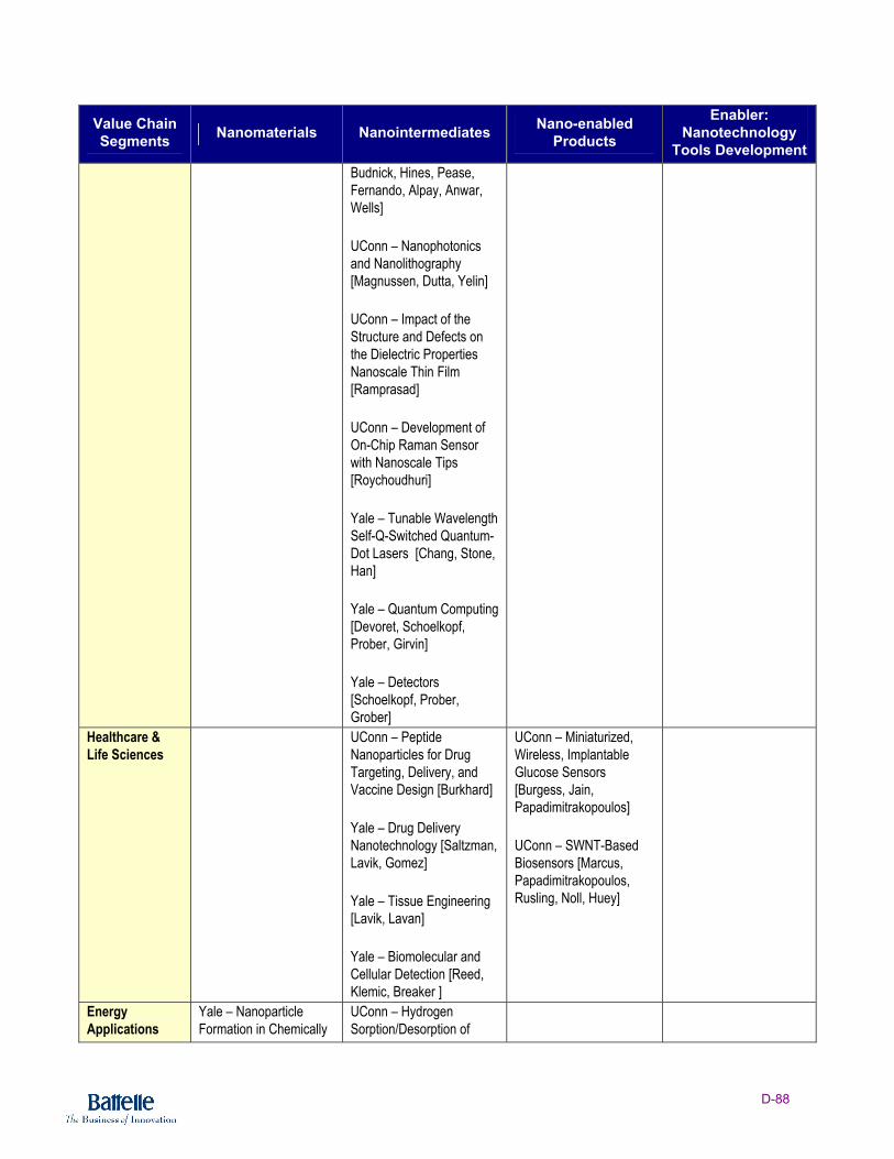
D-88
Value Chain Segments Nanomaterials Nanointermediates Nano-enabled
Products
Enabler: Nanotechnology
Tools Development Budnick, Hines, Pease, Fernando, Alpay, Anwar, Wells] UConn – Nanophotonics and Nanolithography [Magnussen, Dutta, Yelin] UConn – Impact of the Structure and Defects on the Dielectric Properties Nanoscale Thin Film [Ramprasad] UConn – Development of On-Chip Raman Sensor with Nanoscale Tips [Roychoudhuri] Yale – Tunable Wavelength Self-Q-Switched Quantum-Dot Lasers [Chang, Stone, Han] Yale – Quantum Computing [Devoret, Schoelkopf, Prober, Girvin] Yale – Detectors [Schoelkopf, Prober, Grober]
Healthcare & Life Sciences
UConn – Peptide Nanoparticles for Drug Targeting, Delivery, and Vaccine Design [Burkhard] Yale – Drug Delivery Nanotechnology [Saltzman, Lavik, Gomez] Yale – Tissue Engineering [Lavik, Lavan] Yale – Biomolecular and Cellular Detection [Reed, Klemic, Breaker ]
UConn – Miniaturized, Wireless, Implantable Glucose Sensors [Burgess, Jain, Papadimitrakopoulos] UConn – SWNT-Based Biosensors [Marcus, Papadimitrakopoulos, Rusling, Noll, Huey]
Energy Applications
Yale – Nanoparticle Formation in Chemically
UConn – Hydrogen Sorption/Desorption of
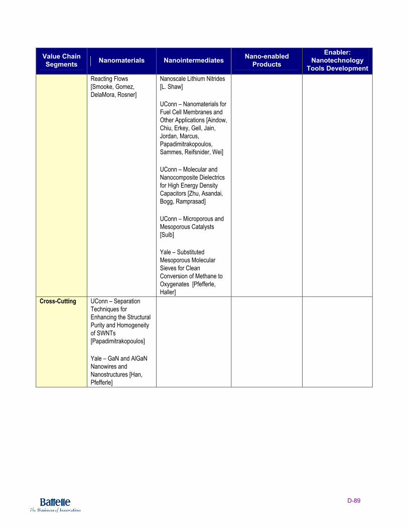
D-89
Value Chain Segments Nanomaterials Nanointermediates Nano-enabled
Products
Enabler: Nanotechnology
Tools Development Reacting Flows [Smooke, Gomez, DelaMora, Rosner]
Nanoscale Lithium Nitrides [L. Shaw] UConn – Nanomaterials for Fuel Cell Membranes and Other Applications [Aindow, Chiu, Erkey, Gell, Jain, Jordan, Marcus, Papadimitrakopoulos, Sammes, Reifsnider, Wei] UConn – Molecular and Nanocomposite Dielectrics for High Energy Density Capacitors [Zhu, Asandai, Bogg, Ramprasad] UConn – Microporous and Mesoporous Catalysts [Suib] Yale – Substituted Mesoporous Molecular Sieves for Clean Conversion of Methane to Oxygenates [Pfefferle, Haller]
Cross-Cutting UConn – Separation Techniques for Enhancing the Structural Purity and Homogeneity of SWNTs [Papadimitrakopoulos] Yale – GaN and AlGaN Nanowires and Nanostructures [Han, Pfefferle]