A Batteryless 19µW MICS/ISM-Band Energy Harvesting Body Area
41
A Batteryless 19μW MICS/ISM- Band Energy Harvesting Body Area Sensor Node SoC Fan Zhang, Yanqing Zhang, Jason Silver, Yousef Shakhsheer, Manohar Nagaraju, Alicia Klinefelter, Jagdish Pandey, James Boley, Eric Carlson, Aatmesh Shrivastava, Brian Otis, Benton Calhoun University of Washington, Seattle, WA University of Virginia, Charlottesville, VA 1
Transcript of A Batteryless 19µW MICS/ISM-Band Energy Harvesting Body Area
A Batteryless 19µW MICS/ISM-
Band Energy Harvesting Body
Area Sensor Node SoC
Fan Zhang, Yanqing Zhang, Jason Silver, Yousef
Shakhsheer, Manohar Nagaraju, Alicia Klinefelter,
Jagdish Pandey, James Boley, Eric Carlson,
Aatmesh Shrivastava, Brian Otis, Benton Calhoun
University of Washington, Seattle, WA
University of Virginia, Charlottesville, VA
1

• Wireless body area sensor nodes (BASN) enable
inexpensive continuous monitoring of patients
• Battery replacement for body-worn devices may not be
feasible or desirable
Information
Assessment,
Treatment
Introduction

Commercial-off-the-shelf (COTS) wireless BASN
Other Components: Amplifiers, ADC, Power, Interface
• RF Transceiver
• Matching network
• RF crystal
• Antenna connector
(bottom) Radio
• PAVG > 20 mW (continuous transmission)
< 2 hours of battery life (33mAh)
• Memory
• Microcontroller
• Watch Crystal
(top)
Digital Logic Memory
3
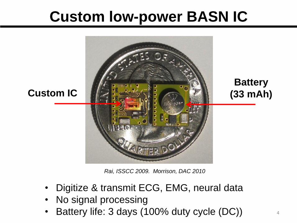
Custom low-power BASN IC
Rai, ISSCC 2009. Morrison, DAC 2010
• Digitize & transmit ECG, EMG, neural data
• No signal processing
• Battery life: 3 days (100% duty cycle (DC)) 4
Custom IC Battery
(33 mAh)
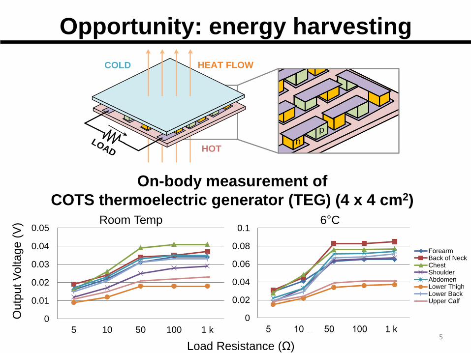
Opportunity: energy harvesting
COLD
HOTn
p
LOAD
HEAT FLOW
0
0.01
0.02
0.03
0.04
0.05
5 10 50 100 1 k
Room Temp
Ou
tput
Vo
ltage (
V)
Load Resistance (Ω) 5
On-body measurement of
COTS thermoelectric generator (TEG) (4 x 4 cm2)
0
0.02
0.04
0.06
0.08
0.1
5 Ω 10 Ω 50 Ω 100 Ω 1 kΩ
6°C
ForearmBack of NeckChestShoulderAbdomenLower ThighLower BackUpper Calf

Opportunity: energy harvesting
COLD
HOTn
p
LOAD
HEAT FLOW
0
0.01
0.02
0.03
0.04
0.05
5 10 50 100 1 k
Room Temp
Ou
tput
Vo
ltage (
V)
Load Resistance (Ω)
~60µW ~200µW
6
On-body measurement of
COTS thermoelectric generator (TEG) (4 x 4 cm2)
0
0.02
0.04
0.06
0.08
0.1
5 Ω 10 Ω 50 Ω 100 Ω 1 kΩ
6°C
ForearmBack of NeckChestShoulderAbdomenLower ThighLower BackUpper Calf
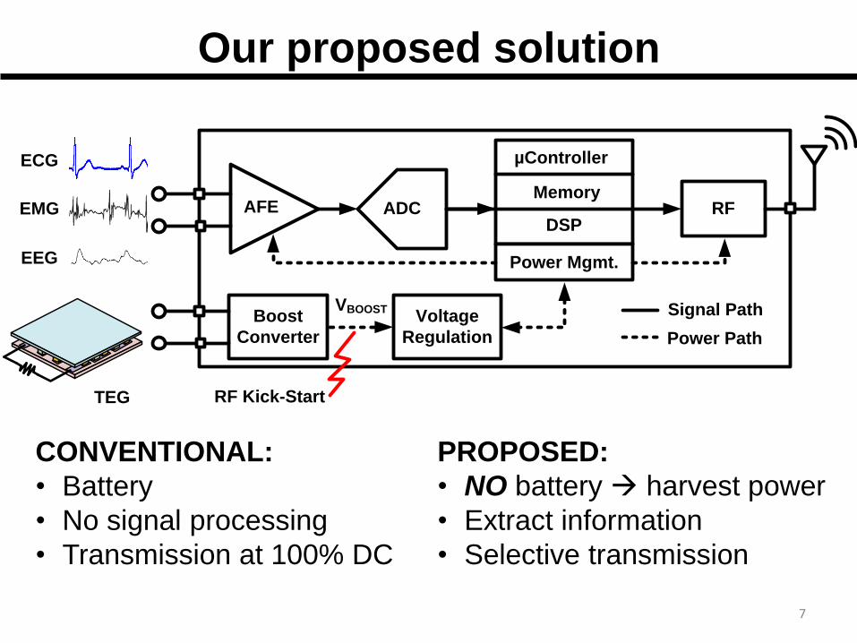
PROPOSED:
• NO battery harvest power
• Extract information
• Selective transmission
Our proposed solution
7
CONVENTIONAL:
• Battery
• No signal processing
• Transmission at 100% DC
ADC RFAFE
Boost
Converter
Voltage
Regulation
µController
Memory
DSP
Power Mgmt.
RF Kick-StartTEG
Signal Path
Power Path
VBOOST
ECG
EMG
EEG
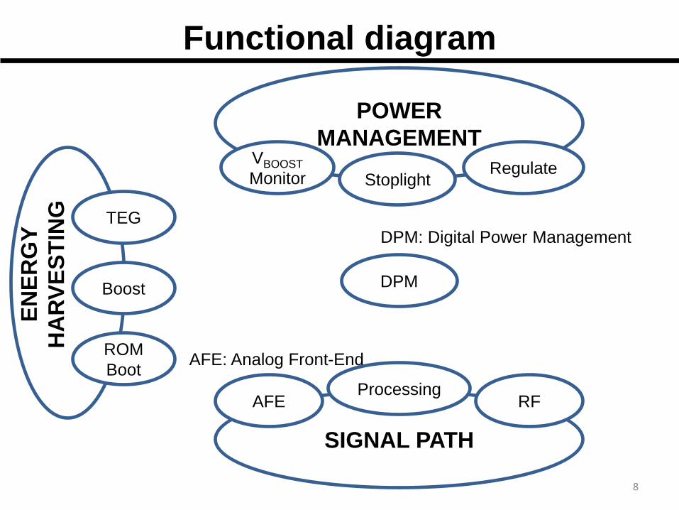
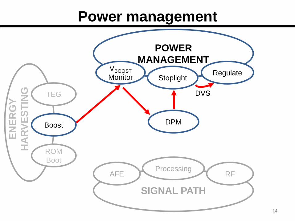
Functional diagram
POWER
MANAGEMENT
Regulate VBOOST
Monitor Stoplight
SIGNAL PATH
AFE Processing
RF
DPM
TEG
Boost
ROM
Boot
EN
ER
GY
HA
RV
ES
TIN
G
8
DPM: Digital Power Management
AFE: Analog Front-End

Startup and energy harvesting
RF-kick
POWER
MANAGEMENT
Regulate VBOOST
Monitor Stoplight
SIGNAL PATH
AFE Processing
RF
DPM
TEG
Boost
ROM
Boot
EN
ER
GY
HA
RV
ES
TIN
G

Startup and energy harvesting
RF-kick
POWER
MANAGEMENT
Regulate VBOOST
Monitor Stoplight
SIGNAL PATH
AFE Processing
RF
DPM
TEG
Boost
ROM
Boot
EN
ER
GY
HA
RV
ES
TIN
G
POR

Signal processing path
11
TEG
Boost
ROM
Boot
POWER
MANAGEMENT
Regulate VBOOST
Monitor Stoplight
EN
ER
GY
HA
RV
ES
TIN
G
SIGNAL PATH
AFE Processing
RF
DPM

Signal processing path
12
TEG
Boost
ROM
Boot
POWER
MANAGEMENT
Regulate VBOOST
Monitor Stoplight
EN
ER
GY
HA
RV
ES
TIN
G
SIGNAL PATH
AFE Processing
RF
DPM
Flexible signal path
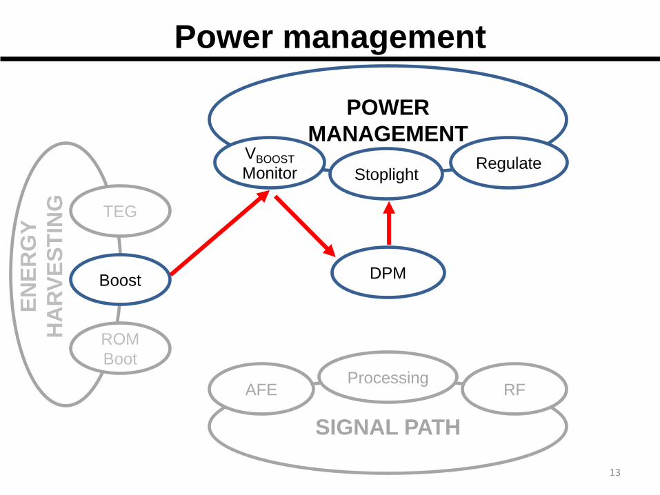
Power management
13
TEG
Boost
ROM
Boot
POWER
MANAGEMENT
Regulate VBOOST
Monitor Stoplight
EN
ER
GY
HA
RV
ES
TIN
G
SIGNAL PATH
AFE Processing
RF
DPM
Power management
14
TEG
Boost
ROM
Boot
POWER
MANAGEMENT
Regulate VBOOST
Monitor Stoplight
EN
ER
GY
HA
RV
ES
TIN
G
SIGNAL PATH
AFE Processing
RF
DPM
DVS

System block diagram
15

Energy harvesting
16
ROM

Hybrid energy harvesting
VBOOST: 1.35V
6 stages
Rectifier
Over-Voltage Clamp
N1
Boost Converter
RF:
-10 dBm
VTEG:
30 mV
Gate
Control
TEG
Power Mgmt.
Storage CapN1
Power-On Reset (POR)
Off-chip
Off-chip
17
Capable of thermal, photovoltaic, and/or RF energy harvesting
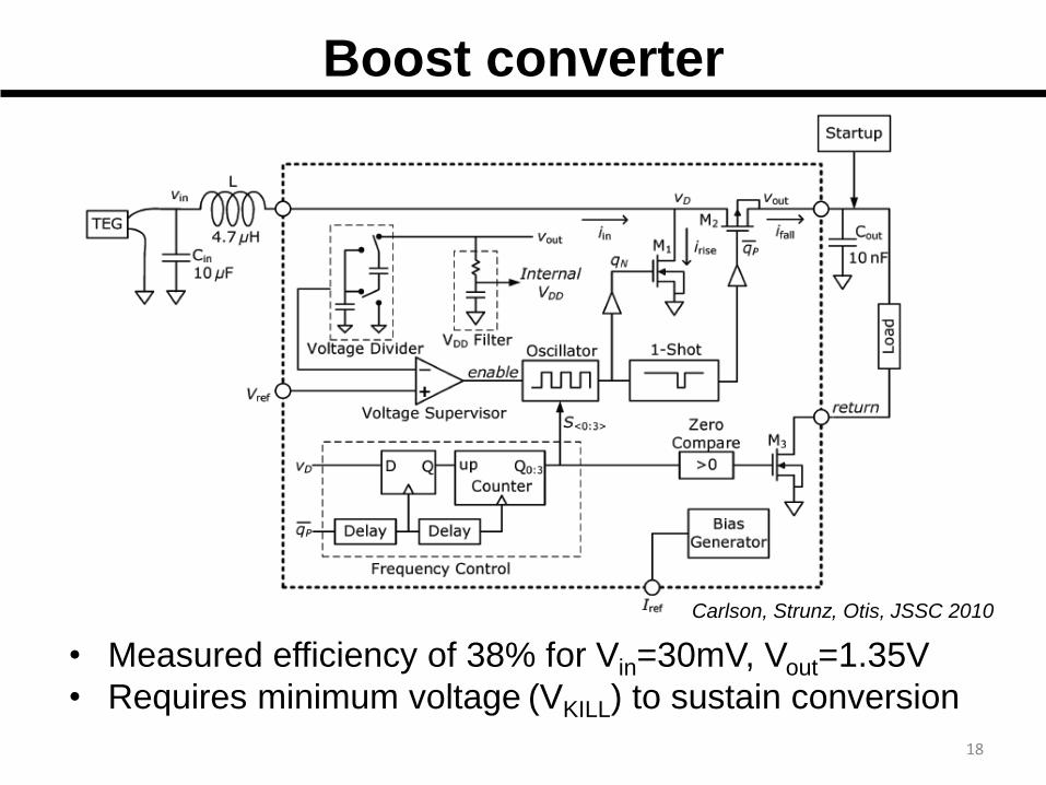
1cm
• Measured efficiency of 38% for Vin=30mV, Vout=1.35V
• Requires minimum voltage (VKILL) to sustain conversion
18
Boost converter
Carlson, Strunz, Otis, JSSC 2010

Measured RF kick-start
0 2 4 6 8 100
0.5
1
1.5
time (s)
Vo
ltag
e (
V)
RF Pulse, -10dBm
Boost Converter
turns on
VBOOST
VTEG
• Wireless RF pulse provides one-time kick-start
• The node runs indefinitely thereafter 19

Boot-up sequence
• POR issues reset at 1.0V
• Upon boot-up, the chip fetches instructions from the ROM
(default) or the RAM
• If VBOOST < VKILL , RF burst can ‘revive’ chip to default
algorithm in ROM
POR
Programmed?
132B ROM
(AFib Detection)
1404B RAM
(Reprogrammable)
Yes No
1.2 V
1 V
VBOOST POR out
20
Instruction memory (IMEM)

Signal path
21

Analog front-end (AFE)
22
AmpOut+
AmpOut-
LNA
Cs
Cf
In+
In-
AmpIn+
AmpIn- GND
Cfilter
Out+
Out-
Gm Gm
Cfilter
Gm Gm
Chopper
modulatorPseudo-resistor
Cs
Cf
Cfilter
Cfilter
VgaOutVGA
CsVgaIn+
VgaIn-Cs
Cf
GmVCM
AmpIn+
Vbias1
Vbias2
VDD
GND
AmpIn-
Vbias3
Am
pO
ut-
Am
pO
ut+
Vcs
CMFB
VgaIn+
Vbias4
Vbias5
VDD
GND
VgaIn-
Vbias6
Vg
aO
ut
Vcs
Cf
Gm
• Chopper-stabilized
low-noise amp
• Variable-gain amp
• 6 programmable
gain 40 – 78 dB
• 3 µW / channel
1 of 4 channels

Flexible signal path
23
Example of Mixed Path
ENV
DetectFIR
Example Custom Path
RR+
AFibFIR
Generic Path
MCU
Flexible Architecture for Data Processing
MCU
Event-Based Burst
Store and Burst
Stream
If event
Processed
Data
Flexible Architecture for Data Transmission
Data for TX
4kB
DMem
4kB
DMem
ECG
EMG
EEG
AFE
Data processing Data transmission
• Data processing: max flexibility (generic path) or max efficiency (biosignal accelerators)
• Data transmission: supports modes from streaming (100% DC) to rare event detection (~0% DC)
MCU: microcontroller
TX

MCU
RR+AFib Accel.
30-Tap FIR Accel.
0 50 100 150 200 Delay (µs)
Measure
d E
nerg
y/O
p (
pJ)
Energy efficient accelerators
24
Accelerators:
• Programmable FIR
• Heart rate (R-R) extraction
• Atrial Fibrillation (AFib) detection
• Band energy extraction
• Direct memory access (DMA)
• Packetizer
Energy Efficiency / Sample
110x
6800x
4000x
0
1
2
3
4
30 Tap FIR MCU 6.3 nJ
Accel 57.6 pJ
Env. Detect MCU 3.6 nJ
Accel 530 fJ
R-R Extract MCU 12 pJ
Accel 3 fJ

25
DPM: signal path control
ADC
DMA/SRAM
Bio-signal
Accelerators
Packetizer
Power and
Channel control
Sa
mp
ling
ra
te c
on
tro
l
Power/clock gate,
clock rate, and
bus control
Du
ty c
ycle
, d
ata
ra
te c
on
tro
l
Dig
itiz
ed V
BO
OS
T
DPM Chip
program
LNA
VBOOST
VGA
IMEM

MCU vs. DPM
26
DPM
MCU
IMEM
• Execution of instructions toggles automatically
between MCU and DPM.
Operation DPM Energy MCU Energy
NOP 0.7 pJ 1.46 pJ
Control Signals 2.8 pJ 2.92 pJ
Branch Commands 2.9 pJ 4.38 pJ
Generic processing
(e.g. add, multiple)
Control instructions
(e.g. power/clock-gate)
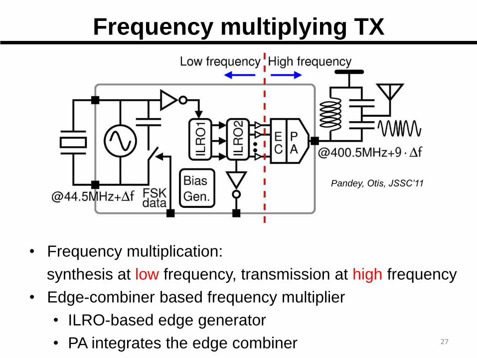
Frequency multiplying TX
Pandey, Otis, JSSC’11
27
• Frequency multiplication:
synthesis at low frequency, transmission at high frequency
• Edge-combiner based frequency multiplier
• ILRO-based edge generator
• PA integrates the edge combiner

BFSK data modulation
FSK Data
CL CL
ΔC
• Quartz reference clock is pulled using DC (~200ppm)
• Δf is multiplied by 9x (~100kHz)
“1” “0”
28
Measured Data Modulation
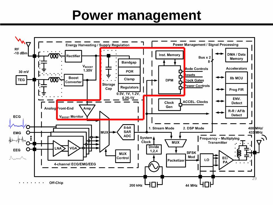
Power management
29

0.5 V
Bandgap
0.5
V0
.5V
1.0
V
1.2
V
F1
F1
F2
F2
0.25-1.0V
VBOOST: 1.35V Linear Regulators Switched-Cap Regulator
Bias Gen
VREF, IREF
30
Voltage regulation
1.2V PADS, AFE
1.0V TX LO
0.5V TX PA
0.5V DPM, MEM, ACCEL
Variable 0.25-1.0V in 50mV, enabling DVS.
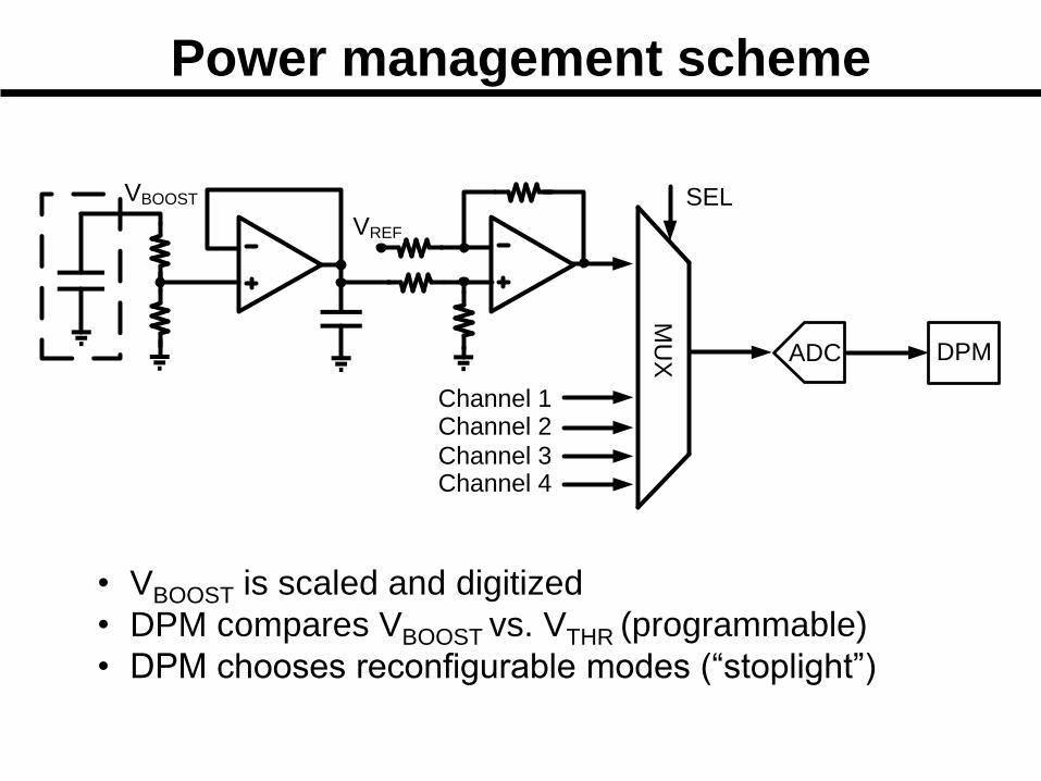
Power management scheme
VREF
MU
XChannel 1
VBOOST
Channel 2
Channel 3Channel 4
ADC
SEL
DPM
• VBOOST is scaled and digitized
• DPM compares VBOOST vs. VTHR (programmable)
• DPM chooses reconfigurable modes (“stoplight”)

Closed-loop power management
VTEG (V)
VBoost VDD, AFE
VGA Out (V)
Supply (V)
TX Duty-
Cycle
Green Yellow Red Yellow Green
Time (s)
32
MODES AFE Process Data Mem. Inst. Mem. Transmit VTHR
1.35 V
1.3 V
1.1 V
0.9 V
Green
Yellow /
Red Sto
pli
gh
t

Continuous transmission of ECG
0.2 0.4 0.6 0.8 1 1.2 1.4 1.6 1.8time (s)
Real ECG
Reconstructed ECG
0.2 0.4 0.6 0.8 1 1.2 1.4 1.6 1.8time (s)
0.2 0.4 0.6 0.8 1 1.2 1.4 1.6 1.8time (s)
0.2 0.4 0.6 0.8 1 1.2 1.4 1.6 1.8
0.2 0.4 0.6 0.8 1 1.2 1.4 1.6 1.8
2.2 2.4 2.6 2.8 3 3.2 3.4 3.6 3.8 40
0.5
1
TX
D
ata
2.2 2.4 2.6 2.8 3 3.2 3.4 3.6 3.8 40
0.5
1
RX
D
ata
2.2 2.4 2.6 2.8 3 3.2 3.4 3.6 3.8 40
0.5
1
time (ms)
RX
Clo
ck
1.798 1.7981 1.7982 1.7983 1.7984 1.7985 1.7986
0
0.5
1
TX
EN
1.7979 1.798 1.7981 1.7982 1.7983 1.7984 1.7985 1.7986 1.7987
0
0.5
1
TX
data
time (s)
Header(5b) Data(16b) CRC(3b)
655msVBOOST
sample
2
1
1
0
1
01
0
1
01
0
1
0.5
0 0.2 0.4 0.6 0.8 1.0 1.2 1.4 1.6 1.8
0 0.2 0.4 0.6 0.8 1.0 1.2 1.4 1.6 1.8Time (s)
Time (s)
Vo
lta
ge
(mV
)T
X
Da
ta
RX
Da
ta
RX
Clo
ck
AD
C i
n(V
)T
X
Da
ta
TX
EN
Raw-Data Mode:
R-R Mode:
1.2ms
650µs
TX DATA
RX DATA
RX CLK
Voltage
(mV)
Time (s)
• ECG signal measured from a healthy human subject
• Wireless link demonstrated between the custom IC and a
commercial receiver (TI CC1101)
• 397 µW from VBOOST
33

R-R interval extraction of ECG
0.2 0.4 0.6 0.8 1 1.2 1.4 1.6 1.8
0.4
0.6
0.8
1
0.2 0.4 0.6 0.8 1 1.2 1.4 1.6 1.8
0
0.5
1
0.2 0.4 0.6 0.8 1 1.2 1.4 1.6 1.8
0
0.5
1
1.798 1.7981 1.7982 1.7983 1.7984 1.7985 1.7986
0
0.5
1
1.7979 1.798 1.7981 1.7982 1.7983 1.7984 1.7985 1.7986 1.7987
0
0.5
1
655 ms
650 µs
Header Data CRC
VBoost
sample
ADC IN
(V)
TX EN
TX
DATA
Time (s)
• Every 5s, VBOOST is sampled to check for sufficient energy
• DPM enables RF crystal oscillator (20ms) and TX (650µs)
• 19 µW from VBOOST
• Powered from a 30mV input 34
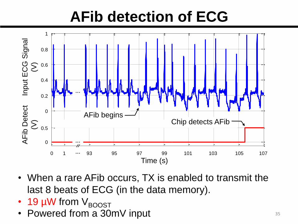
Time (s) 0 1 93 95 97 99 101 103 105 107
1
…
…
…
AFib begins Chip detects AFib
0.8
0.6
0.4
0.2
0
0.5
0
AFib detection of ECG
• When a rare AFib occurs, TX is enabled to transmit the
last 8 beats of ECG (in the data memory).
• 19 µW from VBOOST
• Powered from a 30mV input 35
Input E
CG
Sig
nal
(V)
AF
ib D
ete
ct
(V)

0 20 40 60 800
100
200
300
400
500
Selective transmission
AFE
(4µA)
Supply
Regulation
(3µA)
Digital
(4.6µA)
TX
(0.14µA) Clock
Gen
(2µA)
36
Effective Transmit Rate (kbps)
Estim
ate
d T
ota
l chip
Pow
er
(µW
)
Battery-free with TEGs today
• Selective TX and ULP circuits enable energy harvesting
With next-generation
TEGs
TX DC: 0.013%

SoC die photo
0.13 µm CMOS 2.5
mm
3.3 mm 37

This Work Kim
VLSI'11
Rai
ISSCC’09
Verma
JSSC’10
Yan
JSSC'11
Chen
ISSCC'10
Sensors ECG, EMG,
EEG ECG
Neural, ECG,
EMG, EEG EEG
ECG,
TIV
Temp,
Pressure
Supply
Voltage
30 mV,
-10 dBm 1.2 V 1 V 1 V 1.2 V 0.4/0.5 V
E Harvesting Thermal, RF Solar
Supply Reg.
AFE 4-ch 3-ch 1-ch 18-ch 4-ch N/A
TX datarate 200 kb/s 100 kb/s
1 Mbps
(On-body
link)
TX PDC
(100% on) 160 µW 400 µW 2.8 mW
TX POUT -18.5 dBm -16 dBm -6 dBm
TX band 402 / 433
MHz
402 / 433
MHz 20-40 MHz
Power Mgmt.
Clock +
Power gating,
DPM
Clock
gating
Power
gating
DVS
Comparison with prior work

Comparison with prior work (cont.) This Work
Kim
VLSI'11
Rai
ISSCC’09
Verma
JSSC’10
Yan
JSSC'11
Chen
ISSCC'10
Micro-
processor
1.5 pJ/Inst
200kHz
(8b RISC ISA)
28.9 pJ/Inst
73kHz
(32b COR-
M3)
Accelerator
Prog. FIR,
AFIB, DMA,
Env. Det.,
Packetizer
4x SIMD,
FIR, DMA,
Encryption ASIC DSP
FIR,
Packetizer,
Compression
Memory 5.5kB (0.3-
0.7V) 42kB (1.2V) 20kB (1.2V) 5kB (0.4V)
Dig. Power 2.1µW ~12µW N/A 2.1µW 500µW 2.1µW
(MCU)
Total Power 19µW 31.1µW 500µW 77.1µW 2.4mW 7.7µW
Note on
Total Power
(includes):
8b ADC, DSP
(R-R extract),
TX at 0.013%
DC
12b ADC,
DSP
(heart beat
detection)
8b ADC,
TX at
100%
DC
12b ADC,
DSP (EEG
feature
extraction)
10b ADC,
DSP (data
comp, FIR),
SRAM, TX at
5% DC
Data
acquisition,
DSP (DFT),
SRAM
Technology 130nm 180nm 130nm 180nm 180nm 180nm

Conclusion
1. First wireless biosignal processing chip powered solely from a TEG with RF kickstart enabling battery-free operation
2. Our chip integrates state-of-the-art MICS/ISM transmitter, AFE, powertrain, and biosignal accelerators
3. These blocks are intelligently controlled to enable programmable datapath and closed-loop power management
40

Thank you!
41