
A battery monitoring IC with an isolated communication ...
12
A battery monitoring IC with an isolated communication interface for electric vehicles Tong Wang 1,2a) , Ye Zhao 1 , and Jie Chen 1 1 Institute of Microelectronics of Chinese Academy of Sciences, Beijing, 100029, China 2 School of Microelectronics of University of Chinese Academy of Sciences, Beijing, 100049, China a) [email protected] Abstract: This paper presents a Li-ion battery monitoring and protection IC suitable for monitoring 12 battery cells for electric vehicles (EVs). A two-wire, transformer based, isolated interface is proposed to provide the interface for the cascaded ICs. The interface uses the “balanced” two-wire technology and encodes the four SPI signals into DC-free pulse that can be coupled by a transformer, which features high-speed, low electromagnetic interference (EMI), and reliable data transmission. The IC was fabricated in a 0.18 μm, 60 V BCD process, with a total chip area of 4.4 × 3.6 mm 2 . Measurement results show that the proposed interface can achieve a data rate up to 1 Mbps. Meanwhile, the measured current consumption is less than 45 μA in sleeping mode. Keywords: battery monitoring, isolated interface, SPI, electric vehicle, BMS Classification: Integrated circuits References [1] A. Affanni, et al.: “Battery choice and management for new-generation electric vehicles,” IEEE Trans. Ind. Electron. 52 (2005) 1343 (DOI: 10.1109/TIE.2005. 855664). [2] Linear Technology, Inc.: LTC6802 Datasheet (2009) http://www.linear.com. [3] K. Kadirvel, et al.: “A stackable, 6-cell, li-ion, battery management IC for electric vehicles with 13, 12-bit ADCs, cell balancing, and direct-connect current-mode communications,” IEEE J. Solid-State Circuits 49 (2014) 928 (DOI: 10.1109/JSSC.2014.2300861). [4] R. Kliger: “Integrated transformer-coupled isolation,” IEEE Instrum. Meas. Mag. 6 (2003) 16 (DOI: 10.1109/MIM.2003.1184271). [5] C. H. Hsu, et al.: “On the implementation of CAN buses to battery management systems,” IEEE International Midwest Symposium on Circuits and Systems (2011) 1 (DOI: 10.1109/MWSCAS.2011.6026561). [6] V. R. H. Lorentz, et al.: “Novel cost-efficient contactless distributed monitoring concept for smart battery cells,” IEEE International Symposium on Industrial Electronics (2012) 1342 (DOI: 10.1109/ISIE.2012.6237285). [7] S. Kaeriyama, et al.: “A 2.5 kV isolation 35 kV/us CMR 250 Mbps digital © IEICE 2018 DOI: 10.1587/elex.15.20180513 Received May 18, 2018 Accepted May 28, 2018 Publicized June 12, 2018 Copyedited June 25, 2018 1 LETTER IEICE Electronics Express, Vol.15, No.12, 1–12
Transcript of A battery monitoring IC with an isolated communication ...

A battery monitoring IC withan isolated communicationinterface for electric vehicles
Tong Wang1,2a), Ye Zhao1, and Jie Chen11 Institute of Microelectronics of Chinese Academy of Sciences,
Beijing, 100029, China2 School of Microelectronics of University of Chinese Academy of Sciences,
Beijing, 100049, China
Abstract: This paper presents a Li-ion battery monitoring and protection
IC suitable for monitoring 12 battery cells for electric vehicles (EVs). A
two-wire, transformer based, isolated interface is proposed to provide the
interface for the cascaded ICs. The interface uses the “balanced” two-wire
technology and encodes the four SPI signals into DC-free pulse that can be
coupled by a transformer, which features high-speed, low electromagnetic
interference (EMI), and reliable data transmission. The IC was fabricated in
a 0.18µm, 60V BCD process, with a total chip area of 4.4 × 3.6mm2.
Measurement results show that the proposed interface can achieve a data rate
up to 1Mbps. Meanwhile, the measured current consumption is less than
45µA in sleeping mode.
Keywords: battery monitoring, isolated interface, SPI, electric vehicle,
BMS
Classification: Integrated circuits
References
[1] A. Affanni, et al.: “Battery choice and management for new-generation electricvehicles,” IEEE Trans. Ind. Electron. 52 (2005) 1343 (DOI: 10.1109/TIE.2005.855664).
[2] Linear Technology, Inc.: LTC6802 Datasheet (2009) http://www.linear.com.[3] K. Kadirvel, et al.: “A stackable, 6-cell, li-ion, battery management IC for
electric vehicles with 13, 12-bit ADCs, cell balancing, and direct-connectcurrent-mode communications,” IEEE J. Solid-State Circuits 49 (2014) 928(DOI: 10.1109/JSSC.2014.2300861).
[4] R. Kliger: “Integrated transformer-coupled isolation,” IEEE Instrum. Meas.Mag. 6 (2003) 16 (DOI: 10.1109/MIM.2003.1184271).
[5] C. H. Hsu, et al.: “On the implementation of CAN buses to batterymanagement systems,” IEEE International Midwest Symposium on Circuitsand Systems (2011) 1 (DOI: 10.1109/MWSCAS.2011.6026561).
[6] V. R. H. Lorentz, et al.: “Novel cost-efficient contactless distributed monitoringconcept for smart battery cells,” IEEE International Symposium on IndustrialElectronics (2012) 1342 (DOI: 10.1109/ISIE.2012.6237285).
[7] S. Kaeriyama, et al.: “A 2.5 kV isolation 35 kV/us CMR 250Mbps digital© IEICE 2018DOI: 10.1587/elex.15.20180513Received May 18, 2018Accepted May 28, 2018Publicized June 12, 2018Copyedited June 25, 2018
1
LETTER IEICE Electronics Express, Vol.15, No.12, 1–12

isolator in standard CMOS with a small transformer driving technique,” IEEEJ. Solid-State Circuits 47 (2012) 435 (DOI: 10.1109/JSSC.2011.2170775).
[8] M. Brandl, et al.: “Batteries and battery management systems for electricvehicles,” Design, Automation and Test in Europe Conference and Exhibition(2012) 971 (DOI: 10.1109/DATE.2012.6176637).
[9] H. J. Hsu and S. Y. Huang: “A low-jitter ADPLL via a suppressive digital filterand an interpolation-based locking scheme,” IEEE Trans. Very Large ScaleIntegr. (VLSI) Syst. 19 (2011) 165 (DOI: 10.1109/TVLSI.2009.2030410).
[10] S. Byun: “A 400Mb/s∼2.5Gb/s referenceless CDR IC using intrinsicfrequency detection capability of half-rate linear detector,” IEEE Trans.Circuits Syst. 63 (2016) 1592 (DOI: 10.1109/TCSI.2016.2587751).
[11] Pulse Electronics, Inc.: PE-68386NL Datasheet (2007) http://www.pulseelectronics.com.
1 Introduction
In the Li-ion battery systems for EVs, the battery management system (BMS) is
essential for improving battery life and safety. High precision battery parameters
detection, cell balancing and battery protection are three essential aspects of BMS.
Many battery monitoring ICs [1, 2, 3] have been developed in recent years. In
BMS, the battery pack is usually composed of up to 96 Li-ion batteries in series,
supplying a total voltage near 400V. So multiple cascaded battery monitoring ICs
are required to detect the battery status. The voltage domains of monitoring ICs in
the cascaded chain are different, resulting in a big challenge to design the data bus
interface among the cascaded ICs. The previous works [4, 5] use the optocoupler as
the isolated interface. But the high power consumption, low integration, low speed
(the data rate is generally less than 1Mbps) and degradation of light emitting diode
(LED) limit its application. Digital isolators using magnetic coupling or capacitive
coupling are proposed in [6, 7, 8]. But the magnetic coupling and capacitive
coupling can generate EMI to the surrounding circuits, which reduces the commu-
nication reliability. Besides, the digital isolator needs to provide four isolated
channels for SPI signals and configure four transformers or four pairs of capacitors.
Especially, the digital isolator requires an independent isolated power supply, which
increases the cost and system complexity. In [2], the battery monitoring IC adopts
a 4-wire, current-mode Serial Peripheral Interface (SPI) which allows the IC to be
directly connected to one another without optocouplers or isolators. The ICs can be
daisy-chained to monitor the battery pack. But if one IC in this daisy-chained
system breaks down, the whole network will collapse. So it’s not suitable for
expansion and implement. To resolve all the mentioned problems, a two-wire,
isolated transformer interface is presented in this paper to form a daisy chain bus
configuration between the cascaded ICs. Besides, the IC uses a 12-bit Sigma-Delta
analog-to-digital (�� ADC) to measure voltage and the battery pack temperature.
The cell balancing function and some protection features are also integrated in this
IC to extend battery life and improve system safety.
This paper is organized as follows. Section 2 provides the architecture of the
proposed communication interface. Section 3 describes the implementation details© IEICE 2018DOI: 10.1587/elex.15.20180513Received May 18, 2018Accepted May 28, 2018Publicized June 12, 2018Copyedited June 25, 2018
2
IEICE Electronics Express, Vol.15, No.12, 1–12

of the proposed communication interface. Section 4 provides the experimental
results and compares this work to some published literatures.
2 Architecture of the proposed interface
Fig. 1 shows the symbol connection between the stacked battery monitoring ICs
and a Li-ion battery charger microcontroller (MCU). Multiple ICs can be stacked in
a vertical arrangement in order to monitor up to 96 Li-ion batteries. So the front-end
monitoring ICs work in the high-voltage (HV) domain. When the ICs are connected
to MCU which works in the low-voltage (LV) domain, isolated communication
devices are needed. However, when the ICs and MCU are on the same board, they
can be directly connected. Considering the two applications above, the IC integra-
tes two communication interfaces: SPI and the proposed isolated interface. The SPI
interface is used to link the bottom IC device in the stack to MCU. It’s a standard
interface with a Chip Select (CS), a Clock (SCK), a Master-In-Slave-Out (SDI), and
a Master-Out-Slave-In (SDO). The proposed interface is used to communicate
between the daisy-chained ICs. As shown in Fig. 1, the absolute voltage range of
each monitoring IC increases with its position in the cascaded structure. So the
proposed interface uses the transformer coupling isolation to achieve signal trans-
mission among the stacked ICs. It uses the twisted pair cable as the transmission
medium and encodes the four SPI signals into a balanced two-wire differential
signal that can be transmitted on the twisted pair, which can remove the high
common-mode voltage and cancel out the EMI from external sources. Compared
with the literatures mentioned in the introduction, this method can support data
rates up to 1Mbps and save the design of four isolation channels. Besides, it can
achieve the flexible network configuration of the front-end monitoring ICs.
Fig. 2 shows the block diagram of the monitoring IC and a conceptual
architecture of the proposed interface. The proposed interface consists of two pairs
Fig. 1. The application of the battery monitoring IC
© IEICE 2018DOI: 10.1587/elex.15.20180513Received May 18, 2018Accepted May 28, 2018Publicized June 12, 2018Copyedited June 25, 2018
3
IEICE Electronics Express, Vol.15, No.12, 1–12

of bidirectional ports which are high ports (ISOH+/-) and low ports (ISOL+/-).Ports ISOH+/- are the high-side interfaces that communicate with the top side
device while the ISOL+/- are the low-side interfaces to connect to the bottom-side
device. Every pair of bidirectional port consists of a balanced transmission driver, a
differential receiver and a pulse codec module.
3 Circuit description
3.1 Transmitter and receiver
As shown in Fig. 2, the transmitter adopts a current-regulated differential driver and
the receiver is designed as a window comparator with a differential voltage
threshold. The transmitter drive current is designed to be 20 � Ibias and the com-
parator voltage threshold is half of the voltage on the COMP pin. The drive current
and the voltage threshold can be set by two external resistors ðR1; R2Þ between the
BIAS pin and GND. A 2.5V reference drives the BIAS pin. So the current Ibiasflowing through the resistance R1 and R2 can be calculated as follows:
Ibias ¼ 2:5V
R1 þ R2
ð1Þ
Then the drive current Idrive is written as follows:
Idrive ¼ 20 � Ibias ð2ÞThe comparator voltage threshold VTHR can be written as
VTHR ¼ VCOMP
2¼ Ibias � R2
2ð3Þ
where VCOMP is the voltage on the COMP pin.
Fig. 3 shows the schematic of the transmitter and its connection to the load
resistance RM and the external transformer U1. When the switch POS is closed and
the switch NEG is off, the ISOH/L+ port sources current and the ISOH/L- port
sinks current, then it can generate a positive voltage between the two ports across
the load resistor RM. On the contrary, when the switch NEG is closed and the
switch POS is off, the ISOH/L+ port sinks current and the ISOH/L- port sources
current, then it generates a negative voltage. When not transmitting, the two ports
maintain the voltage near VDD through a pair of 35K resistors. The isolation
barrier U1 adopts a transformer with a 1:1 turns ratio. So the transmitted differential
signal amplitude VA can be calculated as follows:
Fig. 2. Block diagram of the IC and the proposed interface
© IEICE 2018DOI: 10.1587/elex.15.20180513Received May 18, 2018Accepted May 28, 2018Publicized June 12, 2018Copyedited June 25, 2018
4
IEICE Electronics Express, Vol.15, No.12, 1–12
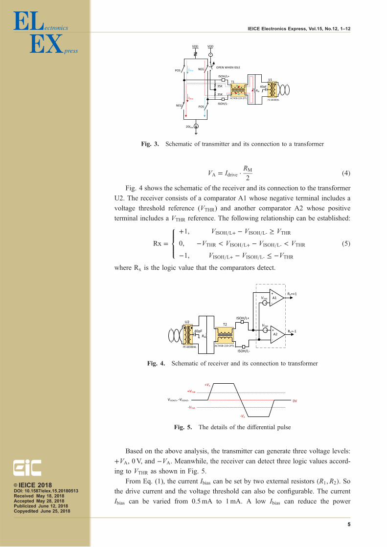
VA ¼ Idrive � RM
2ð4Þ
Fig. 4 shows the schematic of the receiver and its connection to the transformer
U2. The receiver consists of a comparator A1 whose negative terminal includes a
voltage threshold reference (VTHR) and another comparator A2 whose positive
terminal includes a VTHR reference. The following relationship can be established:
Rx ¼þ1; VISOH=L+ � VISOH=L- � VTHR
0; �VTHR < VISOH=L+ � VISOH=L- < VTHR
�1; VISOH=L+ � VISOH=L- � �VTHR
8><>: ð5Þ
where Rx is the logic value that the comparators detect.
Based on the above analysis, the transmitter can generate three voltage levels:
þVA, 0V, and �VA. Meanwhile, the receiver can detect three logic values accord-
ing to VTHR as shown in Fig. 5.
From Eq. (1), the current Ibias can be set by two external resistors ðR1; R2Þ. Sothe drive current and the voltage threshold can also be configurable. The current
Ibias can be varied from 0.5mA to 1mA. A low Ibias can reduce the power
Fig. 3. Schematic of transmitter and its connection to a transformer
Fig. 4. Schematic of receiver and its connection to transformer
Fig. 5. The details of the differential pulse
© IEICE 2018DOI: 10.1587/elex.15.20180513Received May 18, 2018Accepted May 28, 2018Publicized June 12, 2018Copyedited June 25, 2018
5
IEICE Electronics Express, Vol.15, No.12, 1–12

consumption while a high Ibias can increase the amplitude of VA, which means that
we can configure the current Ibias according to the different application scenarios
and requirements. When the communication distance (the length of twisted pair)
is long or the working environment is poor, we can increase the current Ibias to
compensate for the increased insertion loss in the cable and increase the noise
immunity. However, when the application has certain requirements on the power
consumption or the communication distance is short, we can choose to reduce the
current Ibias. The typical configuration is shown in Table I.
3.2 Coding and decoding scheme
The working environment of the BMS inside the car is very poor. There are many
surge and pulse interference signals. In order to eliminate the DC signal compo-
nents and enhance the reliability, we adopt a novel encoding method. We define
pulses as the symmetric pulse pairs. A +1 pulse pair is defined as a þVA pulse
followed by a �VA pulse. A −1 pulse pair is defined as a �VA pulse followed by a
+VA pulse. In order to distinguish the signal type, five kinds of effective signals are
generated via the combination of pulse width and polarity as shown in Table II. A
pulse with 400 ns duration (200 ns+200 ns) is used to transmit CS changing and a
pulse with 250 ns duration (125 ns+125 ns) is used to transmit SDI signal. A pulse
with 100 ns duration (50 ns+50 ns) is used to transmit SDO signal and correspond-
ing SCK falling edge signal.
Fig. 6 is the communication sequence diagram that illustrates how a bidirec-
tional communication interface configured as a master interacts with another
interface configured as a slave. The master IC initiates communication by lowing
CS, then the transmitter converts this transition into a −1 pulse. The pulse traverses
the isolation barrier and arrives at the slave IC’s interface. Once confirmed, the −1pulse is converted back to a falling CS transition. The master uses the SCK rising
edge to latch SDI data. Every SDI signal is encoded into a +1 or −1 pulse. When
the slave IC receives the pulse, it will set the slave SDI to the proper state. It should
Table I. Typical parameter values
Parameter R1 R2 Ibias Idrive VTHR RM VA
Config. 1 3800Ω 1200Ω 0.5mA 10mA 0.3V 120Ω 0.6V
Config. 2 1900Ω 600Ω 1mA 20mA 0.3V 120Ω 1.2V
Table II. Communication events and the pulse type
Pulsetype
Commu.events
CS rising CS falling SDI ¼ 1 SDI ¼ 0SDO ¼ 0/SCK falling
Pulsewidth
200 ns+200 ns 200 ns+200 ns 125 ns+125 ns 125 ns+125 ns 50 ns+50 ns
© IEICE 2018DOI: 10.1587/elex.15.20180513Received May 18, 2018Accepted May 28, 2018Publicized June 12, 2018Copyedited June 25, 2018
6
IEICE Electronics Express, Vol.15, No.12, 1–12

be noticed that if the slave SDO ¼ 1, the slave IC does not transmit a pulse and the
master IC sets the master SDO ¼ 1. At the end of the communication, the master IC
raises CS. This CS changing is transmitted to the slave IC in the form of a +1 pulse,then the slave CS will rise to high state.
It should be noticed that there is no explicit clock signal connected between the
upper and lower ICs. In order to achieve clock synchronization, we use an all-
digital clock and data recovery circuit (CDR) to ensure the reliable serial commu-
nication [9, 10]. The transmitter embeds the clock signal into the data stream, and
then the receiver extracts the clock signal by the CDR and uses this extracted clock
for sampling and decoding. When multiple ICs are connected in series, a corre-
sponding address must be assigned to each device. Address 0x01 is assigned to the
bottom IC which is directly connected to MCU, and the non-zero addresses are
assigned to the other ICs accordingly. All commands sent by MCU originate in the
stack from the bottom IC, and then pass through the middle ICs up to the top IC.
The IC responds to commands, measures and reports the data back to MCU when
the address matches.
3.3 Selection of the transformer type
The transformer can isolate the DC voltages and remove the high voltage common
mode signals. But the actual transformer cannot be completely coupled because of
the leakage flux, which causes the insertion loss. The insertion loss can attenuate
signal energy and cause the waveform distortion. The insertion loss (IL) can be
calculated as:
IL ¼ �10 log U
ð1 � �ÞU����
����2 !
¼ �20 log 1
1 � �
��������
� �ð6Þ
where U is the source voltage and Δ is the ratio of pulse fading. The relationship
between the transformer magnetizing inductance Ld and Δ can be described as:
Ld ¼ � � R
�ð7Þ
Fig. 6. Schematic diagram of the communication sequence
© IEICE 2018DOI: 10.1587/elex.15.20180513Received May 18, 2018Accepted May 28, 2018Publicized June 12, 2018Copyedited June 25, 2018
7
IEICE Electronics Express, Vol.15, No.12, 1–12

where τ is the pulse width and R is the equivalent resistance of transformer primary
loop. It can be calculated as:
R ¼ r0 � RL
r0 þ RL¼ RM
2¼ 60� ð8Þ
where r0 and RL are the source internal resistance and the load resistance,
respectively. In order to increase the system reliability, the IL should be less than
−1.5 dB. Referring to Eq. (6), (7) and (8), the magnetizing inductance Ld should be
more than 50µH. Fig. 7 shows the pulse waveforms through the transformer with
different magnetizing inductance Ld. It can be seen that the insertion loss IL
increases with the increasing of the magnetizing inductance Ld. Finally, in this
work we choose the PE-68386NL transformer with a magnetizing inductance of
785 µH [11].
4 Chip fabrication and measurement results
The proposed Li-ion battery monitoring IC was implemented using 0.18 µm, 60V
BCD process, with a total chip area of 4:4 � 3:6mm2. Fig. 8 shows the chip
micrograph. Fig. 9 shows the measurement setup. Two ICs connect together to
communicate with an ARM development board. Addresses (0x01, 0x02) are
assigned to every IC in the stack correspondingly. All commands from the ARM
board originate in the stack from the bottom IC to the top IC. A PC connected to the
ARM board is used to provide a graphic user interface.
Fig. 7. Pulse waveforms through a transformer with different Ld
Fig. 8. Chip micrograph of the battery monitoring IC
© IEICE 2018DOI: 10.1587/elex.15.20180513Received May 18, 2018Accepted May 28, 2018Publicized June 12, 2018Copyedited June 25, 2018
8
IEICE Electronics Express, Vol.15, No.12, 1–12

If no valid communication event happens in a given time 2 s, the chip will go to
the sleeping mode to reduce power consumption. The SPI interface and the isolated
interface can be woken up by the falling edge of CS and the differential pulse on the
twisted pair, respectively. The measured wake-up process is shown in Fig. 10. For
the bottom IC (0x01), about 3.2 µs after the CS falling edge, the SPI interface
wakes up and the BIAS pin settles to its final value of 2.5V. About 0.6 µs later, the
bottom IC sends a differential pulse which persists for 300 ns or longer to the upper
IC by ISOH+ and ISOH-. About 4.1 µs after the upper IC (0x02) receives the
differential pulse, the isolated interface wakes up and its BIAS pin rises to 2.5V.
When the chip operates in sleeping mode and operating mode, the measured current
consumption are 45µA and 560µA, respectively.
In this test, we select the bottom IC with address 0x01 to measure the cell
voltage. The voltages of the 12 batteries are detected repeatedly over 500 times
at room temperature. 20 groups of detecting results and error distribution of the
battery 6 is shown in Fig. 11. The results show that this monitoring IC can measure
the voltage of each battery cell precisely with a max detecting error of 2mV.
Fig. 12 shows the measurement results of four communication events. All of
these events, CS falling, CS rising, SDI, SDO, demonstrate the same pulse width
Fig. 9. Photo of the measurement setup
(a) (b)
Fig. 10. Communication wake up: (a) SPI interface wake up, (b)isolated interface wake up
© IEICE 2018DOI: 10.1587/elex.15.20180513Received May 18, 2018Accepted May 28, 2018Publicized June 12, 2018Copyedited June 25, 2018
9
IEICE Electronics Express, Vol.15, No.12, 1–12

and polarity as shown in Table II. Fig. 13 shows the scope plot of the transmission
data between MCU and the bottom IC. The SPI frequency is 1MHz. The data
writing from MCU to bottom IC is realized by SDI. As can be seen, the SDI signal
(1010 0110) can be correctly encoded to corresponding pulses with 250 ns duration
on the twisted pair. Then the bottom IC receives and decodes these pulses into SDI
signal (1010 0110). The reading data signal from the bottom IC to MCU is realized
by SDO. The SDO signal (1010 0110) can also be correctly encoded to pulses with
100 ns duration on the twisted pair. The MCU receives these pulses and sets SDO to
the proper state. So every communication event can be transmitted correctly, which
Fig. 11. Transmission data between MCU and the bottom IC
(a) (b)
(c) (d)
Fig. 12. Communication events: (a) CS falling, (b) CS rising, (c) SDOsignal, (d) SDI signal
© IEICE 2018DOI: 10.1587/elex.15.20180513Received May 18, 2018Accepted May 28, 2018Publicized June 12, 2018Copyedited June 25, 2018
10
IEICE Electronics Express, Vol.15, No.12, 1–12

ensures that all digital data can be transferred correctly by this bus, including the
control commands, battery voltages, temperatures and battery conditions.
The performance of this work is summarized and compared with some similar
ICs from industry and academia in Table III. The proposed IC has the high voltage
measurement accuracy which is 2mV. The novel isolated communication interface
can achieve a data rate up to 1Mbps. Most important of all, this isolated interface
can encode four SPI signals into a balanced two-wire differential signal that can be
transmitted on the twisted pair, which features low EMI, high noise immunity, and
reliable data transmission.
Fig. 13. Transmission data between MCU and the bottom IC
Table III. Performance summary and comparison
Properties This work [1] [2] [3]
Year 2017 2005 2009 2014
Number of batterychannels
12 10 12 6
Max. battery packvoltage (V)
60 50 60 30
ADC type12-bit
�� ADCNo ADC
12-bit�� ADC
12-bit�� ADC
Voltage accuracy(mV)
2 (5V input) 0.5% 9.2 (5V input) 5 (5V input)
Commu. interfaceSPI, isolatedinterface
Optocoupler SPI SPI, UART
Max. data rate(Mbps)
1 �1 1 N.A
Interface isolationscheme
Transformerisolation
Optocouplerisolation
No externalcomponents
No externalcomponents
Standby current(µA)
45 N.A 62.5 15
Standby power loss(mW)
2.7(VDD ¼ 60V)
N.A3.75
(VDD ¼ 60V)0.6
(VDD ¼ 30V)
© IEICE 2018DOI: 10.1587/elex.15.20180513Received May 18, 2018Accepted May 28, 2018Publicized June 12, 2018Copyedited June 25, 2018
11
IEICE Electronics Express, Vol.15, No.12, 1–12

5 Conclusion
A battery monitoring IC with an isolated transformer communication interface has
been implemented in a 0.18 µm, 60V BCD technology. The isolated interface can
provide bidirectional serial communication among the stacked ICs. It uses a simple
pulse transformer as the isolation barrier to achieve hundreds of volts of isolation.
Test results show that the interface can achieve a data rate up to 1Mbps. And the
IC can be daisy-chained to monitor up to 12 series-connected cells with a total
measurement error of less than 2mV. This proposed IC with the isolated interface
can be used in a battery management system to ensure the system security and
increase the battery life.
Acknowledgments
This work was supported by the National Key Research and Development Plan of
China “New Energy Vehicle Special” (2016YFB0100516). The author would like
to thank Dr. Ye Zhao, and Dr. Jie Chen for their useful discussions and instruction.
© IEICE 2018DOI: 10.1587/elex.15.20180513Received May 18, 2018Accepted May 28, 2018Publicized June 12, 2018Copyedited June 25, 2018
12
IEICE Electronics Express, Vol.15, No.12, 1–12