A A K SMC SMB - st.com · R4 to LNB C12 D2 C13 VoRX DETIN VoTX Byp EXTM DSQOUT ADDR R2 (RSEL) ISEL...
13
This is information on a product in full production. May 2013 DocID17882 Rev 4 1/13 13 LNBTVS Transil™ for low noise block protection Datasheet - production data Features Peak pulse power: – up to 3 kW (10/1000 μs) – up to 22.5 kW (8/20 μs) Breakdown voltage range: from 23.1 V to 30 V Low clamping factor Unidirectional with low V F (V F = 1.2 V at 3 A) Low leakage current: 0.2 μA at 25 °C Operating T j max : 150 °C Still IEC 61000-4-5 compliant at T j = 85 °C with standard footprint High power capability at T jmax : – 1250 W (10/1000 μs) JEDEC registered package outline Compatible with LNBH supply and control ICs Complies with the following standards IEC 61000-4-2 level 4: – 15 kV (air discharge) – 8 kV (contact discharge) IEC 61000-4-5 MIL STD 883G, method 3015-7: class 3B: – 25 kV HBM (human body model) Resin meets UL 94, V0 MIL-STD-750, method 2026 solderability EIA STD RS-481 and IEC 60286-3 packing IPC 7531 footprint Description The LNBTVS series has been designed to protect LNB voltage regulators in satellite set top boxes against electrostatic discharges according to IEC 61000-4-2, and MIL STD 883, method 3015, and electrical over stress according to IEC 61000-4-4 and 5. These devices can protect against surges up to 6 kV over the whole consumer temperature range (up to 85 °C). Planar technology makes these devices suitable for high-end set top boxes to provide reliability and stability over time. LNBTVS are packaged in either SMB or SMC (footprints in accordance with IPC 7531 standard). TM: Transil is a trademark of STMicroelectronics K K A A SMC (JEDEC DO-214AB) SMB (JEDEC DO-214AA) Table 1. Device summary Part number I PP A (8/20 μs, IEC 61000-4-5) Package LNBTVS3 250 (3 kV, 12 ) SMB LNBTVS4 334 (4 kV, 12 ) SMC LNBTVS6 500 (6 kV, 12 ) SMC www.st.com
Transcript of A A K SMC SMB - st.com · R4 to LNB C12 D2 C13 VoRX DETIN VoTX Byp EXTM DSQOUT ADDR R2 (RSEL) ISEL...

This is information on a product in full production.
May 2013 DocID17882 Rev 4 1/13
13
LNBTVS
Transil™ for low noise block protection
Datasheet - production data
Features
Peak pulse power:
– up to 3 kW (10/1000 µs)
– up to 22.5 kW (8/20 µs)
Breakdown voltage range: from 23.1 V to 30 V
Low clamping factor
Unidirectional with low VF (VF = 1.2 V at 3 A)
Low leakage current: 0.2 µA at 25 °C
Operating Tj max: 150 °C
Still IEC 61000-4-5 compliant at Tj = 85 °C with standard footprint
High power capability at Tjmax:
– 1250 W (10/1000 µs)
JEDEC registered package outline
Compatible with LNBH supply and control ICs
Complies with the following standards
IEC 61000-4-2 level 4:
– 15 kV (air discharge)
– 8 kV (contact discharge)
IEC 61000-4-5
MIL STD 883G, method 3015-7: class 3B:
– 25 kV HBM (human body model)
Resin meets UL 94, V0
MIL-STD-750, method 2026 solderability
EIA STD RS-481 and IEC 60286-3 packing
IPC 7531 footprint
Description
The LNBTVS series has been designed to protect LNB voltage regulators in satellite set top boxes against electrostatic discharges according to IEC 61000-4-2, and MIL STD 883, method 3015, and electrical over stress according to IEC 61000-4-4 and 5. These devices can protect against surges up to 6 kV over the whole consumer temperature range (up to 85 °C).
Planar technology makes these devices suitable for high-end set top boxes to provide reliability and stability over time.
LNBTVS are packaged in either SMB or SMC (footprints in accordance with IPC 7531 standard).
TM: Transil is a trademark of STMicroelectronics
K K
A A
SMC(JEDEC DO-214AB)
SMB(JEDEC DO-214AA)
Table 1. Device summary
Part numberIPP A (8/20 µs,
IEC 61000-4-5)Package
LNBTVS3 250 (3 kV, 12 ) SMB
LNBTVS4 334 (4 kV, 12 ) SMC
LNBTVS6 500 (6 kV, 12 ) SMC
www.st.com

Characteristics LNBTVS
2/13 DocID17882 Rev 4
1 Characteristics
Figure 1. Electrical characteristics - definitions
Figure 2. Pulse definition for electrical characteristics
Table 2. Absolute maximum ratings (Tamb = 25 °C)
Symbol Parameter Value Unit
PPP Peak pulse power dissipation(1) (8/20 µs) Tj initial = Tamb up to 22.5 kW
Tstg Storage temperature range -65 to + 150 °C
Tj Operating junction temperature range -55 to + 150 °C
TL Maximum lead temperature for soldering during 10 s. 260 °C
1. For a surge greater than the maximum values, the diode will fail in short-circuit.
Table 3. Thermal parameter
Symbol Parameter Value Unit
Rth(j-l) Junction to leadsSMC 15 °C/W
SMB 20 °C/W
VCLVBR VRM
IRM
IR
IPP
V
I
IF
VFVCLVBR VRM
IRM
IR
IPP
V
I
IF
VF
UnidirectionalSymbol ParameterV Stand-off voltageV Breakdown voltageV Clamping voltageI Leakage current @ VI Peak pulse current
T Voltage temperature coefficientV Forward voltage drop
RM
BR
CL
RM RM
PP
F
α
100
50
0
Pulse waveformtr = rise time (µs)tp = pulse duration time (µs)
t
%IPP
tptr
DocID17882 Rev 4 3/13
LNBTVS Characteristics
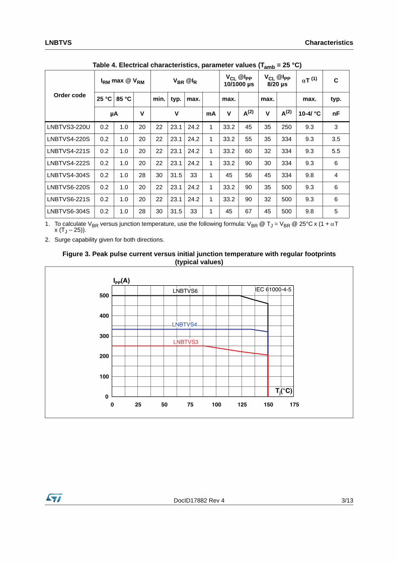
Figure 3. Peak pulse current versus initial junction temperature with regular footprints (typical values)
Table 4. Electrical characteristics, parameter values (Tamb = 25 °C)
Order code
IRM max @ VRM VBR @IR VCL @IPP
10/1000 µsVCL @IPP 8/20 µs
T (1) C
25 °C 85 °C min. typ. max. max. max. max. typ.
µA V V mA V A(2) V A(2) 10-4/ °C nF
LNBTVS3-220U 0.2 1.0 20 22 23.1 24.2 1 33.2 45 35 250 9.3 3
LNBTVS4-220S 0.2 1.0 20 22 23.1 24.2 1 33.2 55 35 334 9.3 3.5
LNBTVS4-221S 0.2 1.0 20 22 23.1 24.2 1 33.2 60 32 334 9.3 5.5
LNBTVS4-222S 0.2 1.0 20 22 23.1 24.2 1 33.2 90 30 334 9.3 6
LNBTVS4-304S 0.2 1.0 28 30 31.5 33 1 45 56 45 334 9.8 4
LNBTVS6-220S 0.2 1.0 20 22 23.1 24.2 1 33.2 90 35 500 9.3 6
LNBTVS6-221S 0.2 1.0 20 22 23.1 24.2 1 33.2 90 32 500 9.3 6
LNBTVS6-304S 0.2 1.0 28 30 31.5 33 1 45 67 45 500 9.8 5
1. To calculate VBR versus junction temperature, use the following formula: VBR @ TJ = VBR @ 25°C x (1 + T x (TJ – 25)).
2. Surge capability given for both directions.
0
100
200
300
400
500
0 25 50 75 100 125 150 175
LNBTVS6
LNBTVS4
LNBTVS3
I (A)PP
T (°C)j
IEC 61000-4-5

Characteristics LNBTVS
4/13 DocID17882 Rev 4
Figure 4. Surge test examples at +4 kV - IEC 61000-4-5, R = 12
Figure 5. Surge test examples at 334 A and 500 A - IEC 61000-4-5, R = 2
LNBTVS4-221S
LNBTVS6-221S
LNBTVS4-220S
LNBTVS4-304S LNBTVS6-304S
LNBTVS6-304S
334.0 A
500.0 A
334.0 A
DocID17882 Rev 4 5/13
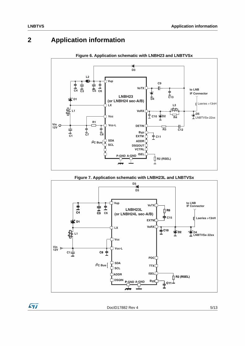
LNBTVS Application information
2 Application information
Figure 6. Application schematic with LNBH23 and LNBTVSx
Figure 7. Application schematic with LNBH23L and LNBTVSx
D3
C11
R4
to LNB
C12
D2
C13
VoRX
DETIN
VoTX
BypEXTM
DSQOUT
ADDR
R2 (RSEL)
ISEL
C9
VCTRL
D4
C10
L3
R3
D5LNBTVSx-22xx
IF Connector
Lseries >13nH
L1
C6C3 C5
L2
Vin12V
{I2C BusSDASCL
LX
Vup
Vcc-L
Vcc
C1 C8C7
R1
D1
C4
P-GND A-GND
LNBH23(or LNBH24 sec-A/B)
to LNB
D4LNBTVSx-22xx
IF Connector
Lseries >13nH
D3
D3
L1
C6
Vin12V
D2D2
SDA
SCL
PDC
LX
Vup
Vcc-L
Vcc
VoRX
EXTM
ADDR
C1 C8C8
TTX
PP-GND A-GND
D1D1
C10C10
C4C4
VoTX
ISELR2 (RSEL)R2 (RSEL)
BypC11C11C11
DSQIN
C15
R9R9C3C3C3
{I2C Bus
LNBH23L(or LNBH24L sec-A/B)

Application information LNBTVS
6/13 DocID17882 Rev 4
Figure 8. Application schematic with LNBH25/26 and LNBTVSx
LNBHxx output is usually connected to the antenna cable of digital satellite receivers. Atmospheric phenomenon can cause high voltage discharges on the antenna cable causing damages to the attached devices.
In applications where it is required to be protected against lightning surges, transient voltage suppressor (TVS) devices like LNBTVSx-22xx can be used to protect LNBHxx and the other devices electrically connected to the antenna cable.
The LNBTVSx-22xx diodes are dedicated lightning and electrical overstress surge protection for LNBHxx voltage regulators. These protection diodes were designed to comply with the stringent IEC 61000-4-5 standard with surges up to 500 A with a whole range of products.
TVS diodes have intrinsic capacitance that attenuates the RF signal. For this reason, the LNBTVSx-22xx cannot be directly connected to the IF (RX/TX) cable connector that carries the RF signals coming from the LNB. To suppress the effect of the intrinsic capacitance, an inductance must be placed in series with the TVS diode (see Figure 9). The goal of the L series and LNBTVC inductance is to be transparent at 22 kHz and to reject frequencies higher than 900 MHz.
The value of the series inductance is usually > 13 nH, with a current capability higher than the Ipp (peak pulse current) expected during the surge.
L1
C3
Vin12V
to LNB IF connector
LX
VupVout
ADDR
C4
LNBH25(or LNBH26 sec - A/B)
{I2C BusSDA
SCL
P-GND A-GND
D1C5
ISELR1 (RSEL)
Byp
C7
DSQIN
C2
C1
Vcc
D2
FLT
DiSEqCEnvelope TTL
or
DiSEqC22KHz TTL
D3
Lseries > 13 nH
D4LNBTVSxx

DocID17882 Rev 4 7/13
LNBTVS Application information
Figure 9. Example of LNBTVS diode connection
D2
VoRX
EXTMLNBH23L
C10
VoTX
C15
R9
D31N4007
D6LNBTVSx-22xx
IF Connector
Lseries >13nH
D2D2
VoRX
EXTMLNBH23L
C10C10
VoTX
C15
R9R9
D31N4007
D6LNBTVSx
IF Connector
Lseries >13nH
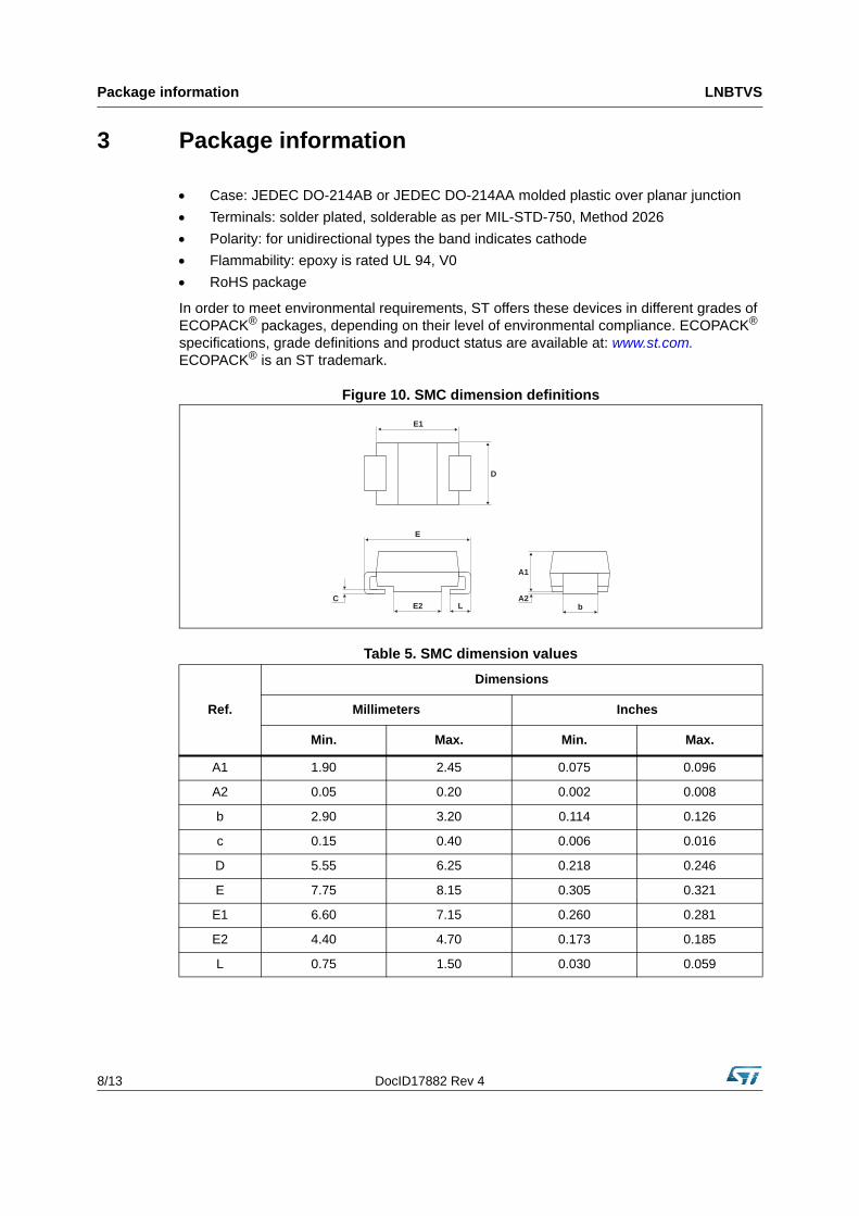
Package information LNBTVS
8/13 DocID17882 Rev 4
3 Package information
Case: JEDEC DO-214AB or JEDEC DO-214AA molded plastic over planar junction
Terminals: solder plated, solderable as per MIL-STD-750, Method 2026
Polarity: for unidirectional types the band indicates cathode
Flammability: epoxy is rated UL 94, V0
RoHS package
In order to meet environmental requirements, ST offers these devices in different grades of ECOPACK® packages, depending on their level of environmental compliance. ECOPACK® specifications, grade definitions and product status are available at: www.st.com. ECOPACK® is an ST trademark.
Figure 10. SMC dimension definitions
Table 5. SMC dimension values
Ref.
Dimensions
Millimeters Inches
Min. Max. Min. Max.
A1 1.90 2.45 0.075 0.096
A2 0.05 0.20 0.002 0.008
b 2.90 3.20 0.114 0.126
c 0.15 0.40 0.006 0.016
D 5.55 6.25 0.218 0.246
E 7.75 8.15 0.305 0.321
E1 6.60 7.15 0.260 0.281
E2 4.40 4.70 0.173 0.185
L 0.75 1.50 0.030 0.059
E
CLE2
E1
D
A1
A2b

DocID17882 Rev 4 9/13
LNBTVS Package information
Figure 11. SMB dimension definitions
Table 6. SMB dimension values
Ref.
Dimensions
Millimeters Inches
Min. Max. Min. Max.
A1 1.90 2.45 0.075 0.096
A2 0.05 0.20 0.002 0.008
b 1.95 2.20 0.077 0.087
c 0.15 0.40 0.006 0.016
D 3.30 3.95 0.130 0.156
E 5.10 5.60 0.201 0.220
E1 4.05 4.60 0.159 0.181
L 0.75 1.50 0.030 0.059
Figure 12. SMC footprint dimensions in mm (inches)
Figure 13. SMB footprint dimensions in mm (inches)
E
CL
E1
D
A1
A2b
8.19
1.545.111.54
(0.061) (0.201)
(0.322)
(0.124)
(0.061)
3.14
2.60
5.84
1.62
2.18
1.62(0.064) (0.102)
(0.23)
(0.064)
(0.086)

Package information LNBTVS
10/13 DocID17882 Rev 4
Figure 14. Marking layout
Note: Marking layout can vary according to assembly location.
y w wzx x x
e: ECOPACK complianceXXX: MarkingZ: Manufacturing locationY: YearWW: week
Cathode bar (unidirectional devices only )

DocID17882 Rev 4 11/13
LNBTVS Ordering information
4 Ordering information
Figure 15. Ordering information scheme
Table 7. Ordering information
Order code Marking Package Weight (g) Base qty Delivery mode
LNBTVS3-220U LC SMB 0.107 2500 Tape and reel
LNBTVS4-220S LAA SMC 0.245 2500 Tape and reel
LNBTVS4-221S LAB SMC 0.245 2500 Tape and reel
LNBTVS4-222S LAC SMC 0.245 2500 Tape and reel
LNBTVS6-220S LBA SMC 0.245 2500 Tape and reel
LNBTVS6-221S LBB SMC 0.245 2500 Tape and reel
LNBTVS4-304S LAD SMC 0.245 2500 Tape and reel
LNBTVS6-304S LBC SMC 0.245 2500 Tape and reel
LNB TVS x - VV x x
Low noise block regulator
Transient voltage suppressor
Lightning surge level
VBR min
VCL
Package
3 = 250 A4 = 334 A6 = 500 A
0 = 35 V1 = 32 V2 = 30 V4 = 45 V
U = SMBS = SMC

Revision history LNBTVS
12/13 DocID17882 Rev 4
5 Revision history
Table 8. Document revision history
Date Revision Changes
30-Aug-2010 1First release. This document merges and updates the content of datasheets LNBTVSx-22xx Revision 3, 20-Jan-2007, and LNBTVSx-304 Revision 1, 01-Apr-2008.
22-Oct-2010 2 Updated Figure 13.
05-Sep-2011 3 Added Figure 8.
21-May-2013 4 Added Table 1: Device summary.

DocID17882 Rev 4 13/13
LNBTVS
Please Read Carefully:
Information in this document is provided solely in connection with ST products. STMicroelectronics NV and its subsidiaries (“ST”) reserve theright to make changes, corrections, modifications or improvements, to this document, and the products and services described herein at anytime, without notice.
All ST products are sold pursuant to ST’s terms and conditions of sale.
Purchasers are solely responsible for the choice, selection and use of the ST products and services described herein, and ST assumes noliability whatsoever relating to the choice, selection or use of the ST products and services described herein.
No license, express or implied, by estoppel or otherwise, to any intellectual property rights is granted under this document. If any part of thisdocument refers to any third party products or services it shall not be deemed a license grant by ST for the use of such third party productsor services, or any intellectual property contained therein or considered as a warranty covering the use in any manner whatsoever of suchthird party products or services or any intellectual property contained therein.
UNLESS OTHERWISE SET FORTH IN ST’S TERMS AND CONDITIONS OF SALE ST DISCLAIMS ANY EXPRESS OR IMPLIEDWARRANTY WITH RESPECT TO THE USE AND/OR SALE OF ST PRODUCTS INCLUDING WITHOUT LIMITATION IMPLIEDWARRANTIES OF MERCHANTABILITY, FITNESS FOR A PARTICULAR PURPOSE (AND THEIR EQUIVALENTS UNDER THE LAWSOF ANY JURISDICTION), OR INFRINGEMENT OF ANY PATENT, COPYRIGHT OR OTHER INTELLECTUAL PROPERTY RIGHT.
ST PRODUCTS ARE NOT AUTHORIZED FOR USE IN WEAPONS. NOR ARE ST PRODUCTS DESIGNED OR AUTHORIZED FOR USEIN: (A) SAFETY CRITICAL APPLICATIONS SUCH AS LIFE SUPPORTING, ACTIVE IMPLANTED DEVICES OR SYSTEMS WITHPRODUCT FUNCTIONAL SAFETY REQUIREMENTS; (B) AERONAUTIC APPLICATIONS; (C) AUTOMOTIVE APPLICATIONS ORENVIRONMENTS, AND/OR (D) AEROSPACE APPLICATIONS OR ENVIRONMENTS. WHERE ST PRODUCTS ARE NOT DESIGNEDFOR SUCH USE, THE PURCHASER SHALL USE PRODUCTS AT PURCHASER’S SOLE RISK, EVEN IF ST HAS BEEN INFORMED INWRITING OF SUCH USAGE, UNLESS A PRODUCT IS EXPRESSLY DESIGNATED BY ST AS BEING INTENDED FOR “AUTOMOTIVE,AUTOMOTIVE SAFETY OR MEDICAL” INDUSTRY DOMAINS ACCORDING TO ST PRODUCT DESIGN SPECIFICATIONS.PRODUCTS FORMALLY ESCC, QML OR JAN QUALIFIED ARE DEEMED SUITABLE FOR USE IN AEROSPACE BY THECORRESPONDING GOVERNMENTAL AGENCY.
Resale of ST products with provisions different from the statements and/or technical features set forth in this document shall immediately voidany warranty granted by ST for the ST product or service described herein and shall not create or extend in any manner whatsoever, anyliability of ST.
ST and the ST logo are trademarks or registered trademarks of ST in various countries.Information in this document supersedes and replaces all information previously supplied.
The ST logo is a registered trademark of STMicroelectronics. All other names are the property of their respective owners.
© 2013 STMicroelectronics - All rights reserved
STMicroelectronics group of companies
Australia - Belgium - Brazil - Canada - China - Czech Republic - Finland - France - Germany - Hong Kong - India - Israel - Italy - Japan - Malaysia - Malta - Morocco - Philippines - Singapore - Spain - Sweden - Switzerland - United Kingdom - United States of America
www.st.com

![Journal of Materials Chemistry C c6tc05574e€¦ · A molecular PTM, 1-[C 6H 13NH][18-crown-6][ClO 4] monohydrate (1), has been synthesized, showing Q4 reversible switchable dielectric](https://static.fdocuments.us/doc/165x107/6081babb6af1d00dc61a9c39/journal-of-materials-chemistry-c-a-molecular-ptm-1-c-6h-13nh18-crown-6clo.jpg)