A 900W, 300V to 50V Dc-dc Power Converter with a 30MHz...
8
A 900W, 300V to 50V Dc-dc Power Converter with a 30MHz Switching Frequency John S. Glaser ([email protected]) Jeffrey Nasadoski Electronic Power Conversion Lab General Electric Global Research Richard Heinrich Naval Electronics & Surveillance Systems Lockheed Martin Corporation Abstract—Designers of power conversion circuits are under relentless pressure to increase power density while maintaining high efficiency. A primary path to higher power density is the use of increased switching frequency. In this paper it is argued that the use of switching frequencies in the VHF band (30MHz-300MHz) are a viable path to the achievement of substantive gains in power density. Evidence for this viewpoint is presented in the form of an unregulated 900W prototype dc-dc converter with a 30MHz switching frequency, an input voltage range of 270VDC to 330VDC, and an output voltage of 50VDC. This converter uses a quad module architecture with series input and parallel output to provide acceptable efficiency with the specified input voltage range. This converter operates with peak output power of 1kW at 330VDC input, and has an efficiency of >78% under nominal conditions, with maximum efficiency near 80%. I. I NTRODUCTION Designers of DC-DC power converters are under re- lentless pressure to increase power density, efficiency, and reliability, reduce cost, and improve transient re- sponse, preferably achieving all these goals simulta- neously. In reality, all these parameters must be bal- anced in a manner that best meets the needs of the application, and certain goals will have priority based on that application. For example, aerospace applications often have restrictions on overall system mass, which results in high power density as a primary goal. This paper promotes the use of switching frequencies in the VHF (very high frequency, 30MHz-300MHz) band as a promising approach to provide substantial gains in power density. A key contributor to power converter volume is the required energy storage, normally implemented with ca- pacitors and inductors [1]. For a given energy storage technology, the size of the storage elements is usually a monotonically increasing function of the energy stored. Increased power density requires reduced stored energy and/or increased storage density. The latter is subject to fundamental material limitations such as breakdown volt- age and permittivity for capacitors, and saturation flux density and permeability for inductors [2]. Improvement in the properties of magnetic and dielectric materials is a slow process. The alternative to increased energy density is the reduction of the stored energy per cycle. This is accomplished by increasing the switching frequency F SW . This works up to a point, but as F SW continues to increase, increased switching losses, proximity losses and core losses in magnetic components, and problems with parasitic reactances diminish these gains. While these issues can be mitigated to some extent, at a high enough frequency they dominate the converter design. Further increases in F SW eventually lead to reduced power density [1, 3, 4]. It has been proposed that a large jump in switching frequency to the VHF band and a move to a new set of topologies and architectures can provide a way to move beyond the limitations of present technology. The paper gives a short overview of approaches to VHF dc-dc power conversion. It shows an approach to 978-1-422-2812-0/09/$25.00 ©2009 IEEE 1121
-
Upload
truongcong -
Category
Documents
-
view
219 -
download
0
Transcript of A 900W, 300V to 50V Dc-dc Power Converter with a 30MHz...
A 900W, 300V to 50V Dc-dc Power Converterwith a 30MHz Switching Frequency
John S. Glaser ([email protected])Jeffrey Nasadoski
Electronic Power Conversion LabGeneral Electric Global Research
Richard HeinrichNaval Electronics & Surveillance Systems
Lockheed Martin Corporation
Abstract—Designers of power conversion circuits areunder relentless pressure to increase power density whilemaintaining high efficiency. A primary path to higherpower density is the use of increased switching frequency. Inthis paper it is argued that the use of switching frequenciesin the VHF band (30MHz-300MHz) are a viable path to theachievement of substantive gains in power density. Evidencefor this viewpoint is presented in the form of an unregulated900W prototype dc-dc converter with a 30MHz switchingfrequency, an input voltage range of 270VDC to 330VDC,and an output voltage of 50VDC. This converter uses a quadmodule architecture with series input and parallel outputto provide acceptable efficiency with the specified inputvoltage range. This converter operates with peak outputpower of 1kW at 330VDC input, and has an efficiency of>78% under nominal conditions, with maximum efficiencynear 80%.
I. INTRODUCTION
Designers of DC-DC power converters are under re-lentless pressure to increase power density, efficiency,and reliability, reduce cost, and improve transient re-sponse, preferably achieving all these goals simulta-neously. In reality, all these parameters must be bal-anced in a manner that best meets the needs of theapplication, and certain goals will have priority basedon that application. For example, aerospace applicationsoften have restrictions on overall system mass, whichresults in high power density as a primary goal. Thispaper promotes the use of switching frequencies in theVHF (very high frequency, 30MHz-300MHz) band as apromising approach to provide substantial gains in power
density.A key contributor to power converter volume is the
required energy storage, normally implemented with ca-pacitors and inductors [1]. For a given energy storagetechnology, the size of the storage elements is usually amonotonically increasing function of the energy stored.Increased power density requires reduced stored energyand/or increased storage density. The latter is subject tofundamental material limitations such as breakdown volt-age and permittivity for capacitors, and saturation fluxdensity and permeability for inductors [2]. Improvementin the properties of magnetic and dielectric materials is aslow process. The alternative to increased energy densityis the reduction of the stored energy per cycle. Thisis accomplished by increasing the switching frequencyFSW .
This works up to a point, but as FSW continues toincrease, increased switching losses, proximity lossesand core losses in magnetic components, and problemswith parasitic reactances diminish these gains. Whilethese issues can be mitigated to some extent, at a highenough frequency they dominate the converter design.Further increases in FSW eventually lead to reducedpower density [1, 3, 4]. It has been proposed that alarge jump in switching frequency to the VHF band anda move to a new set of topologies and architectures canprovide a way to move beyond the limitations of presenttechnology.
The paper gives a short overview of approaches toVHF dc-dc power conversion. It shows an approach to
978-1-422-2812-0/09/$25.00 ©2009 IEEE 1121
2
increase the practical bus voltage for such convertersby a factor of two or more. Experimental evidence forthis approach is presented in the form of an unregu-lated 900W prototype dc-dc converter with a 30MHzswitching frequency, an input voltage range of 270VDCto 330VDC, and an output voltage of 50VDC. Thisconverter uses a quad-module architecture with seriesinput and parallel output to provide acceptable efficiencywith the specified input voltage range. This converter hasan efficiency of >78% under nominal conditions, withmaximum efficiency near 80%.
II. MOTIVATION FOR VHF SWITCHING FREQUENCIES
The point was raised that increased power density viaincreased switching frequency has practical limitations.Thus, how does a >10X jump in FSW provide a patharound these limitations?
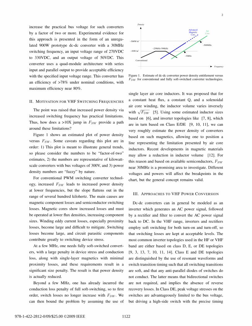
Figure 1 shows an estimated plot of power densityversus FSW . Some caveats regarding this plot are inorder: 1) This plot is meant to illustrate general trends,so please consider the numbers to be “factor-of-two”estimates, 2) the numbers are representative of kilowatt-scale converters with bus voltages of 300V, and 3) powerdensity numbers are “fuzzy” by nature.
For conventional PWM switching converter technol-ogy, increased FSW leads to increased power densityat lower frequencies, but the slope flattens out in therange of several hundred kilohertz. The main causes aremagnetic component losses and semiconductor switchinglosses. Magnetic cores show increased losses and mustbe operated at lower flux densities, increasing componentsizes. Winding eddy current losses, especially proximitylosses, become large and difficult to mitigate. Switchinglosses become large, and circuit parasitic componentscontribute greatly to switching device stress.
At a few MHz, one needs fully soft-switched convert-ers, with a large penalty in device stress and conductionloss, along with single-layer magnetics with minimalproximity losses, and these requirements result in asignificant size penalty. The result is that power densityis actually reduced.
Beyond a few MHz, one has already incurred theconduction loss penalty of full soft-switching, so to firstorder, switch losses no longer increase with FSW . Wecan then bound the problem by assuming the use of
Frequency
Power
Density
~250kHz-500kHz
AdvancedMagneticCore
AirCore
Conventional
~50W/in3
~500W/in3
~5MHz
~500MHz
Figure 1. Estimate of dc-dc converter power density entitlement versusFSW for conventional and fully soft-switched converter technologies.
single layer air core inductors. It was proposed that fora constant heat flux, a constant Q, and a solenoidalair core winding, the inductor volume varies inverselywith
!FSW [5]. Using some estimated inductor sizes
based on [6], and inverter topologies like [7, 8], whichare in turn based on Class E/DE [9, 10, 11], we canvery roughly estimate the power density of convertersbased on such magnetics, allowing one to position aline representing the limitation presented by air coreinductors. Recent developments in magnetic materialsmay allow a reduction in inductor volume [12]. Forthis reason and based on available semiconductors, FSW
near 30MHz is a promising area to investigate. Differentvoltages and powers will affect the breakpoints in thechart, but the general concept remains valid.
III. APPROACHES TO VHF POWER CONVERSION
Dc-dc converters can in general be modeled as aninverter which generates an AC power signal, followedby a rectifier and filter to convert the AC power signalback to DC. In the VHF range, inverters and rectifiersemploy soft switching for both turn-on and turn-off, sothat switching losses are kept at acceptable levels. Themost common inverter topologies used in the HF or VHFband are either based on class D, E, or DE topologies[9, 3, 13, 7, 10, 11, 14]. Class E and DE topologiesare distinguished by the use of resonant waveforms andswitch transition timing such that all switching transitionsare soft, and that any anti-parallel diodes of switches donot conduct. The latter means that bidirectional switchesare not required, and implies the absence of reverserecovery losses. In Class DE, peak voltage stresses on theswitches are advantageously limited to the bus voltage,but driving a high-side switch with the precise timing
978-1-422-2812-0/09/$25.00 ©2009 IEEE 1122
3
required becomes difficult as FSW and the bus voltageincreases.
Class E avoids the high-side drive issue via the use ofa single-ended ground-referenced switch, but the trade-off is high device voltage stress. Furthermore, classE inverters are characterized by a fixed relationshipbetween FSW , switch capacitance CSW , dc bus voltageVDC , and power P :
P = K1FSW CSW V 2DC (1)
where K1 is a constant determined by the converterpassive component values. It can further be shown thatthe class E inverter loss due to the switch resistance RSW
can be approximated by
Ploss = K2P 2
V 2DC
RSW (2)
where K2 is another constant determined by the con-verter passive component values. Finally, the normalizedloss is
Ploss
P= K1K2FSW RSW CSW (3)
The RSW CSW product is a figure of merit for a givenswitch technology. Thus, the maximum class E converterefficiency is rigidly tied to the converter specificationsand the switch technology. An illustrative example canbe given by considering a 1kW high-Q class E inverterwith a 300VDC nominal input, and a 90% drain effi-ciency with all losses in the switch. The resulting switchrequirements translate to a 1200V switch with CSW <
19pF and RSW < 4.2!. A typical 1200V RF MOSFETis the IXYS IXZR08N120, with RDS,on = 2.1! atroom temperature, or an estimated 4.2! at operatingtemperature [15]. At 300V, Coss = 80pF. The drain tocase capacitance alone is 33pF; 19pF is far out of reach.Clearly, the standard class E topology is not suitable forthis application.
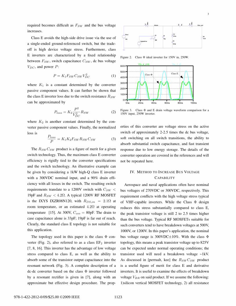
The topology used in this paper is the class " con-verter (Fig. 2), also referred to as a class EF2 inverter[7, 8, 16]. This inverter has the advantage of low voltagestress compared to class E, as well as the ability toabsorb some of the transistor output capacitance into theresonant network (Fig. 3). A complete description of adc-dc converter based on the class " inverter followedby a resonant rectifier is given in [7], along with anapproximate but effective design procedure. The prop-
!"
#$%&'(
$%)
*+
+,-.
/012
+%3
/456789:;7
!(
#33&
!2
+%3&
'"
+.-.)
'2
,&
<+
<=
/895:& /:&;>?16
Figure 2. Class ! ideal inverter for 150V in, 250W.
Figure 3. Class ! and E drain voltage waveform comparison for a150V input, 250W inverter.
erties of this converter are voltage stress on the activeswitch of approximately 2-2.5 times the dc bus voltage,soft switching on all switch transitions, the ability toabsorb substantial switch capacitance, and fast transientresponse due to low energy storage. The details of theconverter operation are covered in the references and willnot be repeated here.
IV. METHOD TO INCREASE BUS VOLTAGE
CAPABILITY
Aerospace and naval applications often have nominalbus voltages of 270VDC or 300VDC, respectively. Thisrequirement conflicts with the high voltage stress typicalof VHF-capable inverters. While the Class " designreduces this stress substantially compared to class E,the peak transistor voltage is still 2 to 2.5 times higherthan the bus voltage. Typical RF MOSFETs suitable forsuch converters tend to have breakdown voltages at 500V,1000V, or 1200V. In this paper’s application, the nominalbus voltage range is 300VDC±10%. With the class "topology, this means a peak transistor voltage up to 825Vcan be expected under normal operating conditions; thetransistor used will need a breakdown voltage ~1kV.As discussed in [perrualt, kee] the RSW CSW productis a useful figure of merit for class E and derivativeinverters. It is useful to examine the effects of breakdownvoltage VBR on said product. If we assume the following:1)silicon vertical MOSFET technology, 2) all resistance
978-1-422-2812-0/09/$25.00 ©2009 IEEE 1123
4
due to drift layer, 3) all capacitance due to body diode,4) uniformly lightly doped drift layer with step junction,5) all structures are planar, and 6) the drift layer becomesfully depleted at the moment the breakdown voltage isreached, then
RSW,sp =WD
qµnNd(4)
CSW,sp =!Si
WD(5)
VBR = 5.3" 1013N! 3
4d (6)
where RSW,sp and CSW,sp area the specific (per area)values, and Eqs. 4, 5, and 6 are from [17]. Then
RSW CSW = RSW,spCSW,sp =!Si
qµnNd(7)
Note that die area has dropped out of the relationship.Equations 7 and 6 can be combined to yield
RSW CSW =!Si
qµn
V43
BR
2.0" 1018(8)
The penalty in normalized conduction loss is seen toincrease as V
43
BR, i.e. a severe penalty is paid for substan-tially increasing the input voltage requirement. This hasstymied the development of VHF converter topologies inmedium voltage applications.
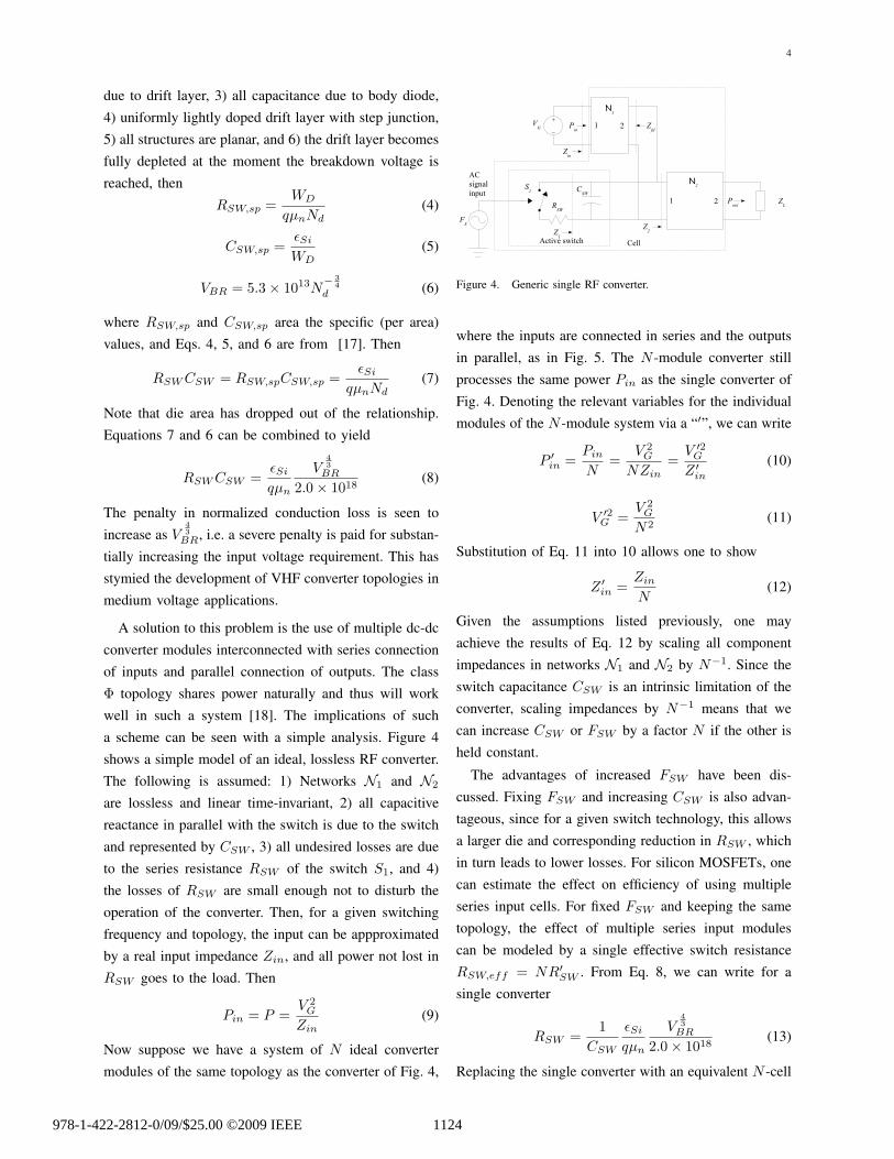
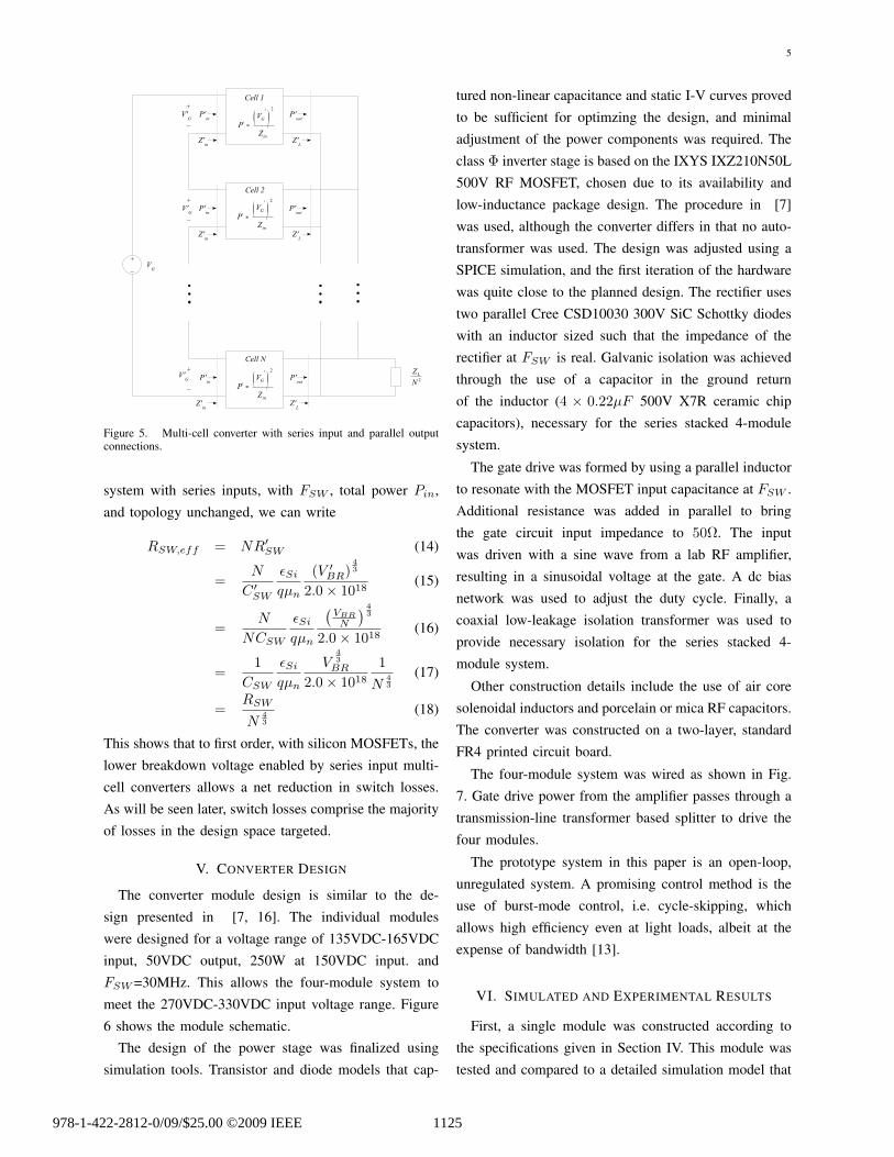
A solution to this problem is the use of multiple dc-dcconverter modules interconnected with series connectionof inputs and parallel connection of outputs. The class" topology shares power naturally and thus will workwell in such a system [18]. The implications of sucha scheme can be seen with a simple analysis. Figure 4shows a simple model of an ideal, lossless RF converter.The following is assumed: 1) Networks N1 and N2
are lossless and linear time-invariant, 2) all capacitivereactance in parallel with the switch is due to the switchand represented by CSW , 3) all undesired losses are dueto the series resistance RSW of the switch S1, and 4)the losses of RSW are small enough not to disturb theoperation of the converter. Then, for a given switchingfrequency and topology, the input can be appproximatedby a real input impedance Zin, and all power not lost inRSW goes to the load. Then
Pin = P =V 2
G
Zin(9)
Now suppose we have a system of N ideal convertermodules of the same topology as the converter of Fig. 4,
+
_
ZL
VG Z
fd
Z2Z
1
CSW
S1
N1
N2
Zin
Pin
1 2
1 2 Pout
Active switch Cell
FS
AC
signal
input
RSW
Figure 4. Generic single RF converter.
where the inputs are connected in series and the outputsin parallel, as in Fig. 5. The N -module converter stillprocesses the same power Pin as the single converter ofFig. 4. Denoting the relevant variables for the individualmodules of the N -module system via a “"”, we can write
P "in =
Pin
N=
V 2G
NZin=
V "2G
Z "in
(10)
V "2G =
V 2G
N2(11)
Substitution of Eq. 11 into 10 allows one to show
Z "in =
Zin
N(12)
Given the assumptions listed previously, one mayachieve the results of Eq. 12 by scaling all componentimpedances in networks N1 and N2 by N!1. Since theswitch capacitance CSW is an intrinsic limitation of theconverter, scaling impedances by N!1 means that wecan increase CSW or FSW by a factor N if the other isheld constant.
The advantages of increased FSW have been dis-cussed. Fixing FSW and increasing CSW is also advan-tageous, since for a given switch technology, this allowsa larger die and corresponding reduction in RSW , whichin turn leads to lower losses. For silicon MOSFETs, onecan estimate the effect on efficiency of using multipleseries input cells. For fixed FSW and keeping the sametopology, the effect of multiple series input modulescan be modeled by a single effective switch resistanceRSW,eff = NR"
SW . From Eq. 8, we can write for asingle converter
RSW =1
CSW
!Si
qµn
V43
BR
2.0" 1018(13)
Replacing the single converter with an equivalent N -cell
978-1-422-2812-0/09/$25.00 ©2009 IEEE 1124
5
!
"!"
#$%&
′
′
=′%&
"
#
!
'
#
!$"
()**+,
()**+-
()**+.
#$%&
#$%&
!$"
!$"
′
′
=′%&
"
#
!
'
#
′
′
=′%&
"
#
!
'
#
#$/
#$/
#$/
#.
#/
'$%&
'$012
!
"
!
"
!
"
'$%&
'$012
'$%&
'$012
Figure 5. Multi-cell converter with series input and parallel outputconnections.
system with series inputs, with FSW , total power Pin,and topology unchanged, we can write
RSW,eff = NR"SW (14)
=N
C "SW
!Si
qµn
(V "BR)
43
2.0" 1018(15)
=N
NCSW
!Si
qµn
!VBRN
" 43
2.0" 1018(16)
=1
CSW
!Si
qµn
V43
BR
2.0" 1018
1N
43
(17)
=RSW
N43
(18)
This shows that to first order, with silicon MOSFETs, thelower breakdown voltage enabled by series input multi-cell converters allows a net reduction in switch losses.As will be seen later, switch losses comprise the majorityof losses in the design space targeted.
V. CONVERTER DESIGN
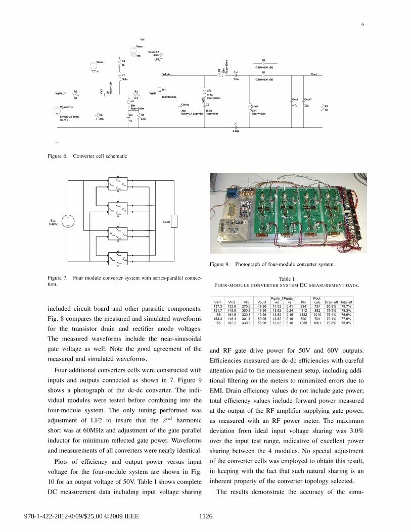
The converter module design is similar to the de-sign presented in [7, 16]. The individual moduleswere designed for a voltage range of 135VDC-165VDCinput, 50VDC output, 250W at 150VDC input. andFSW =30MHz. This allows the four-module system tomeet the 270VDC-330VDC input voltage range. Figure6 shows the module schematic.
The design of the power stage was finalized usingsimulation tools. Transistor and diode models that cap-
tured non-linear capacitance and static I-V curves provedto be sufficient for optimzing the design, and minimaladjustment of the power components was required. Theclass " inverter stage is based on the IXYS IXZ210N50L500V RF MOSFET, chosen due to its availability andlow-inductance package design. The procedure in [7]was used, although the converter differs in that no auto-transformer was used. The design was adjusted using aSPICE simulation, and the first iteration of the hardwarewas quite close to the planned design. The rectifier usestwo parallel Cree CSD10030 300V SiC Schottky diodeswith an inductor sized such that the impedance of therectifier at FSW is real. Galvanic isolation was achievedthrough the use of a capacitor in the ground returnof the inductor (4 " 0.22µF 500V X7R ceramic chipcapacitors), necessary for the series stacked 4-modulesystem.
The gate drive was formed by using a parallel inductorto resonate with the MOSFET input capacitance at FSW .Additional resistance was added in parallel to bringthe gate circuit input impedance to 50!. The inputwas driven with a sine wave from a lab RF amplifier,resulting in a sinusoidal voltage at the gate. A dc biasnetwork was used to adjust the duty cycle. Finally, acoaxial low-leakage isolation transformer was used toprovide necessary isolation for the series stacked 4-module system.
Other construction details include the use of air coresolenoidal inductors and porcelain or mica RF capacitors.The converter was constructed on a two-layer, standardFR4 printed circuit board.
The four-module system was wired as shown in Fig.7. Gate drive power from the amplifier passes through atransmission-line transformer based splitter to drive thefour modules.
The prototype system in this paper is an open-loop,unregulated system. A promising control method is theuse of burst-mode control, i.e. cycle-skipping, whichallows high efficiency even at light loads, albeit at theexpense of bandwidth [13].
VI. SIMULATED AND EXPERIMENTAL RESULTS
First, a single module was constructed according tothe specifications given in Section IV. This module wastested and compared to a detailed simulation model that
978-1-422-2812-0/09/$25.00 ©2009 IEEE 1125
6
D1
CSD10030_GE
D2
CSD10030_GE
Rser=100m
Lrect
73n
Cout
4.7!
Cs1
1.8n
Rs
er=
25
0m
LS
1
130n
IXZ210N50L
M1
Rser=700m
LF2
375n
Rser=0.1 Lser=5n
Cstray
30p
Rser=0.5
LF1
600n
Rser=10m
C2
18.8p
AC 0 0
Vgatedrive
SINE(0 20 30e6)
R3
0.2
Rser=200m
L4
55n
R4
5.6k
R5
215
C3
1n
Rs
er=
10m
Cs
2
2nR6
50
Vbus
150
Vbias
-4
R9
1k
L1
500n
Cout1
20!
C1
0.88!
R1
10
VoutVdrain
Vgate
VC
2
Vgate_in
Vin
Figure 6. Converter cell schematic
Figure 7. Four module converter system with series-parallel connec-tion.
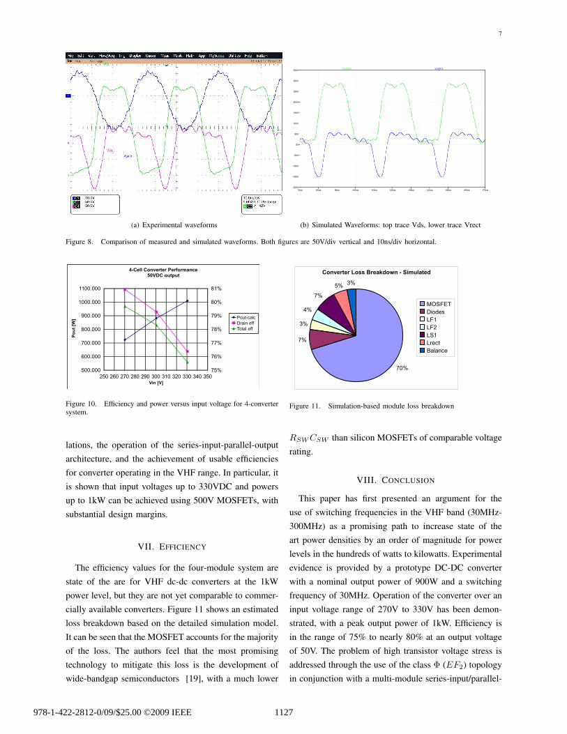
included circuit board and other parasitic components.Fig. 8 compares the measured and simulated waveformsfor the transistor drain and rectifier anode voltages.The measured waveforms include the near-sinusoidalgate voltage as well. Note the good agreement of themeasured and simulated waveforms.
Four additional converters cells were constructed withinputs and outputs connected as shown in 7. Figure 9shows a photograph of the dc-dc converter. The indi-vidual modules were tested before combining into thefour-module system. The only tuning performed wasadjustment of LF2 to insure that the 2nd harmonicshort was at 60MHz and adjustment of the gate parallelinductor for minimum reflected gate power. Waveformsand measurements of all converters were nearly identical.
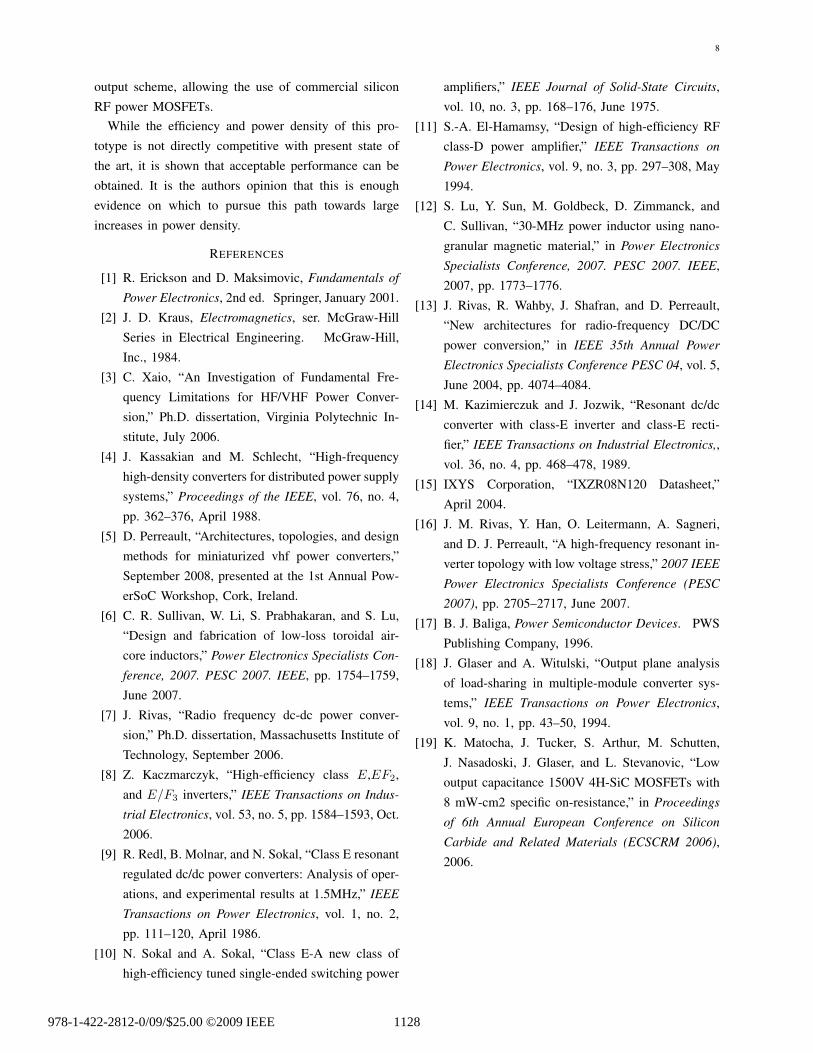
Plots of efficiency and output power versus inputvoltage for the four-module system are shown in Fig.10 for an output voltage of 50V. Table I shows completeDC measurement data including input voltage sharing
Figure 9. Photograph of four-module converter system.
Table IFOUR-MODULE CONVERTER SYSTEM DC MEASUREMENT DATA.
!"#$ !"#% !"# !&'($ )"#
$*+,* $*%,- %+.,% /-,-0 $/,.* .,/$ 1-/ +%/ 1.,-2 +-,+2
$3$,+ $/1,- *..,0 /-,-0 $*,-% .,%/ $$$% 11% +-,*2 +1,*2
$00 $0/,3 **.,3 /-,-0 $*,1% .,$0 $*%% $.$. +0,/2 +3,02
$3*,* $/1,/ *.$,+ 3-,-3 $*,1% .,$0 1-. +./ +-,$2 ++,-2
$01 $0%,% **.,% 3-,-0 $*,-% .,$0 $%33 $..$ +-,12 +1,-2
)45(6789:
)45(67;<=
)&'(>?5@? A;5"#B688 C&(5@B688
and RF gate drive power for 50V and 60V outputs.Efficiencies measured are dc-dc efficiencies with carefulattention paid to the measurement setup, including addi-tional filtering on the meters to minimized errors due toEMI. Drain efficiency values do not include gate power;total efficiency values include forward power measuredat the output of the RF amplifier supplying gate power,as measured with an RF power meter. The maximumdeviation from ideal input voltage sharing was 3.0%over the input test range, indicative of excellent powersharing between the 4 modules. No special adjustmentof the converter cells was employed to obtain this result,in keeping with the fact that such natural sharing is aninherent property of the converter topology selected.
The results demonstrate the accuracy of the simu-
978-1-422-2812-0/09/$25.00 ©2009 IEEE 1126
7
(a) Experimental waveforms
75ns 85ns 95ns 105ns 115ns 125ns 135ns 145ns 155ns 165ns 175ns
-200V
-150V
-100V
-50V
0V
50V
100V
150V
200V
250V
300V
350VV(vdrain) V(n001)
(b) Simulated Waveforms: top trace Vds, lower trace Vrect
Figure 8. Comparison of measured and simulated waveforms. Both figures are 50V/div vertical and 10ns/div horizontal.
!"# !$# !%# !&# !'# (## ()# (!# ((# (*# ("#
"##+###
$##+###
%##+###
&##+###
'##+###
)###+###
))##+###
%",
%$,
%%,
%&,
%',
&#,
&),
!"#$%%&#'()$*+$*&,$*-'*./(0$1234#&'5+65+
-./012342
563789:;;
<.0349:;;
37(&839
,'5+&8:9
Figure 10. Efficiency and power versus input voltage for 4-convertersystem.
lations, the operation of the series-input-parallel-outputarchitecture, and the achievement of usable efficienciesfor converter operating in the VHF range. In particular, itis shown that input voltages up to 330VDC and powersup to 1kW can be achieved using 500V MOSFETs, withsubstantial design margins.
VII. EFFICIENCY
The efficiency values for the four-module system arestate of the are for VHF dc-dc converters at the 1kWpower level, but they are not yet comparable to commer-cially available converters. Figure 11 shows an estimatedloss breakdown based on the detailed simulation model.It can be seen that the MOSFET accounts for the majorityof the loss. The authors feel that the most promisingtechnology to mitigate this loss is the development ofwide-bandgap semiconductors [19], with a much lower
!"#
!#
$#
%#
!#
&#$#
!"#$%&'%&()"**(+&%,-."/#(0(12345,'%.
'()*+,
-./012
3*4
3*5
3)4
36178
9:;:<71
Figure 11. Simulation-based module loss breakdown
RSW CSW than silicon MOSFETs of comparable voltagerating.
VIII. CONCLUSION
This paper has first presented an argument for theuse of switching frequencies in the VHF band (30MHz-300MHz) as a promising path to increase state of theart power densities by an order of magnitude for powerlevels in the hundreds of watts to kilowatts. Experimentalevidence is provided by a prototype DC-DC converterwith a nominal output power of 900W and a switchingfrequency of 30MHz. Operation of the converter over aninput voltage range of 270V to 330V has been demon-strated, with a peak output power of 1kW. Efficiency isin the range of 75% to nearly 80% at an output voltageof 50V. The problem of high transistor voltage stress isaddressed through the use of the class " (EF2) topologyin conjunction with a multi-module series-input/parallel-
978-1-422-2812-0/09/$25.00 ©2009 IEEE 1127
8
output scheme, allowing the use of commercial siliconRF power MOSFETs.
While the efficiency and power density of this pro-totype is not directly competitive with present state ofthe art, it is shown that acceptable performance can beobtained. It is the authors opinion that this is enoughevidence on which to pursue this path towards largeincreases in power density.
REFERENCES
[1] R. Erickson and D. Maksimovic, Fundamentals ofPower Electronics, 2nd ed. Springer, January 2001.
[2] J. D. Kraus, Electromagnetics, ser. McGraw-HillSeries in Electrical Engineering. McGraw-Hill,Inc., 1984.
[3] C. Xaio, “An Investigation of Fundamental Fre-quency Limitations for HF/VHF Power Conver-sion,” Ph.D. dissertation, Virginia Polytechnic In-stitute, July 2006.
[4] J. Kassakian and M. Schlecht, “High-frequencyhigh-density converters for distributed power supplysystems,” Proceedings of the IEEE, vol. 76, no. 4,pp. 362–376, April 1988.
[5] D. Perreault, “Architectures, topologies, and designmethods for miniaturized vhf power converters,”September 2008, presented at the 1st Annual Pow-erSoC Workshop, Cork, Ireland.
[6] C. R. Sullivan, W. Li, S. Prabhakaran, and S. Lu,“Design and fabrication of low-loss toroidal air-core inductors,” Power Electronics Specialists Con-ference, 2007. PESC 2007. IEEE, pp. 1754–1759,June 2007.
[7] J. Rivas, “Radio frequency dc-dc power conver-sion,” Ph.D. dissertation, Massachusetts Institute ofTechnology, September 2006.
[8] Z. Kaczmarczyk, “High-efficiency class E,EF2,and E/F3 inverters,” IEEE Transactions on Indus-trial Electronics, vol. 53, no. 5, pp. 1584–1593, Oct.2006.
[9] R. Redl, B. Molnar, and N. Sokal, “Class E resonantregulated dc/dc power converters: Analysis of oper-ations, and experimental results at 1.5MHz,” IEEETransactions on Power Electronics, vol. 1, no. 2,pp. 111–120, April 1986.
[10] N. Sokal and A. Sokal, “Class E-A new class ofhigh-efficiency tuned single-ended switching power
amplifiers,” IEEE Journal of Solid-State Circuits,vol. 10, no. 3, pp. 168–176, June 1975.
[11] S.-A. El-Hamamsy, “Design of high-efficiency RFclass-D power amplifier,” IEEE Transactions onPower Electronics, vol. 9, no. 3, pp. 297–308, May1994.
[12] S. Lu, Y. Sun, M. Goldbeck, D. Zimmanck, andC. Sullivan, “30-MHz power inductor using nano-granular magnetic material,” in Power ElectronicsSpecialists Conference, 2007. PESC 2007. IEEE,2007, pp. 1773–1776.
[13] J. Rivas, R. Wahby, J. Shafran, and D. Perreault,“New architectures for radio-frequency DC/DCpower conversion,” in IEEE 35th Annual PowerElectronics Specialists Conference PESC 04, vol. 5,June 2004, pp. 4074–4084.
[14] M. Kazimierczuk and J. Jozwik, “Resonant dc/dcconverter with class-E inverter and class-E recti-fier,” IEEE Transactions on Industrial Electronics,,vol. 36, no. 4, pp. 468–478, 1989.
[15] IXYS Corporation, “IXZR08N120 Datasheet,”April 2004.
[16] J. M. Rivas, Y. Han, O. Leitermann, A. Sagneri,and D. J. Perreault, “A high-frequency resonant in-verter topology with low voltage stress,” 2007 IEEEPower Electronics Specialists Conference (PESC2007), pp. 2705–2717, June 2007.
[17] B. J. Baliga, Power Semiconductor Devices. PWSPublishing Company, 1996.
[18] J. Glaser and A. Witulski, “Output plane analysisof load-sharing in multiple-module converter sys-tems,” IEEE Transactions on Power Electronics,vol. 9, no. 1, pp. 43–50, 1994.
[19] K. Matocha, J. Tucker, S. Arthur, M. Schutten,J. Nasadoski, J. Glaser, and L. Stevanovic, “Lowoutput capacitance 1500V 4H-SiC MOSFETs with8 mW-cm2 specific on-resistance,” in Proceedingsof 6th Annual European Conference on SiliconCarbide and Related Materials (ECSCRM 2006),2006.
978-1-422-2812-0/09/$25.00 ©2009 IEEE 1128