A 7.5-GS/s 3.8-ENOB 52-mW flash ADC with clock duty ... 22:3 22 On-chip 3 3:2 1234T 2 1/N clk input...
26
A 7.5-GS/s 3.8-ENOB 52-mW flash ADC with clock duty cycle control in 65nm CMOS Hayun Chung 1 , Alexander Rylyakov 2 , Zeynep Toprak Deniz 2 , John Bulzacchelli 2 , Gu-Yeon Wei 1 , and Daniel Friedman 2 1 Harvard University 2 IBM T. J. Watson Research Center
Transcript of A 7.5-GS/s 3.8-ENOB 52-mW flash ADC with clock duty ... 22:3 22 On-chip 3 3:2 1234T 2 1/N clk input...

A 7.5-GS/s 3.8-ENOB 52-mW flash ADC with clock duty cycle control in 65nm CMOS
Hayun Chung1, Alexander Rylyakov2, Zeynep Toprak Deniz2, John Bulzacchelli2,
Gu-Yeon Wei1, and Daniel Friedman2
1Harvard University2IBM T. J. Watson Research Center

Motivation
ReceiverTransmitter
DigitalequalizerADC
outinChannel
• ADC-based backplane receiver– Portability and design reuse– Power/area scalability with process– FFE + DFE– Equalizer immune to PVT variations

Front-end ADC requirements• High input bandwidth• High sampling rate• Low power consumption• Small area• Coarse resolution acceptable

ADC architecture• 6-7.5 GS/s, 4.5 bit flash ADC
4.5 bitoutput
×22Duty cycle ctrl.
R ladder
Ref.select
22
input Two-stage THA
clk
Two-stage THA
CH
AV ≅ 1CH
AV ≅ 1
Ccomp
input outputclk clk_b
1st stage 2nd stage• Separate 1st stage input from heavily
loaded 2nd stage output• High input bandwidth• Low power

Two-stage THA
CH
AV ≅ 1CH
AV ≅ 1
Ccomp
input outputclk clk_b
(a)(b)
(c)
T H
T H
(a)
(b)
(c)
50% duty cycle50 50

Two-stage THA
CH
AV ≅ 1CH
AV ≅ 1
Ccomp
input outputclk clk_b
(a)(b)
(c)
T H
T H
(a)
(b)
(c)
Duty cycle control42 58

Clock duty cycle control• Extend tracking time in 2nd stage• Sampling rate improvement
– Up to 14% (clock duty cycle: 50 58%)– Enables 7.5 GS/s
• Power savings– THA and duty cycle ctrl. block each
consume 8% of the total ADC power

Two-stage THA
1st stage 2nd stage
biasbias
clk clk_b

Two-stage THA
biasbias
clk
clk_b
clk_b
clk clk
• Charge Injection cancellation

Two-stage THA
biasbias
clk
clk_b
clk_b
clk clk
• Cross-coupled capacitors– Reduces glitching

Comparators
bias
inn inprefn refpLatchesand FFs
out
• Use minimum size transistors– Reduces total capacitive load on THA
output– Suffers from large offset (+/- 3 LSB)

Comparator offset correction
• Reference voltage pre-distortion• Comparator reassignment
8:1
0.5
LSB
+/-1
.75
LSB
ref_sel[7:0]in
outref

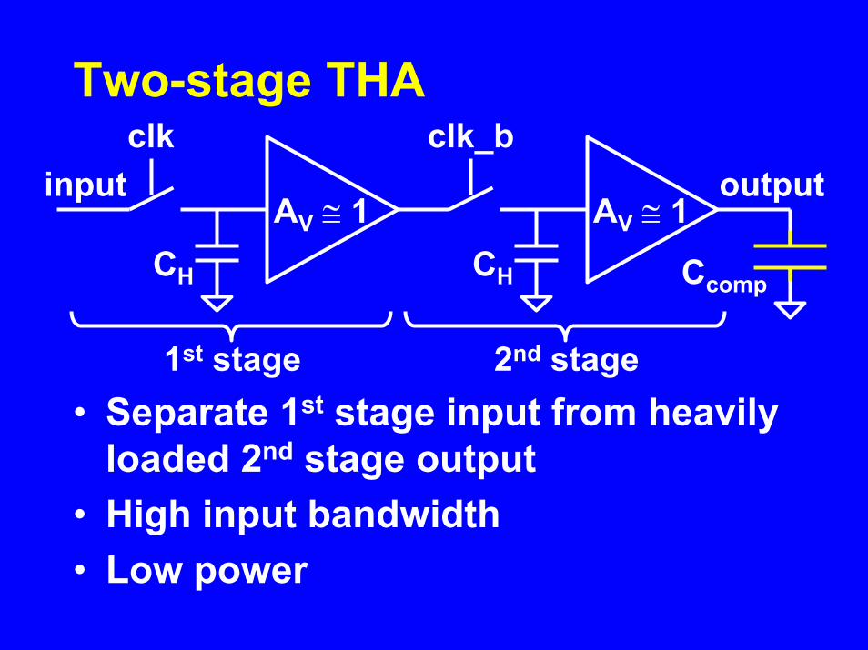
Comparator offset correction
THA
out
put
THA input
• THA buffer non-linearity correction
Comparator offset correction
THA
out
put
ADC output codeV
ref
THA input
• THA buffer non-linearity correction

Measurements
• Challenges in FFT measurements– Reading out high speed, multi-bit ADC
outputs at once– Synchronizing input and clock
generators with good precision

Measurements: SetupOscilloscope
ADC
22:3
22
On-chip
3
3:2
1 2 3 4 T2
1/N
clk
input
sel sel_man
trigger
• Reconstruct full ADC output by realigning measured data with respect to the trigger signal

5 10 15 20-4-2024
Comparator count
INL
(LSB
)
-4-2024
INL
(LSB
)
Measurements: Offset calib.
• INL: 2.6 LSB (before), 0.38 LSB (after)
Aftercalibration
Beforecalibration

5 10 15 20-4-2024
Comparator count
DN
L (L
SB)
-4-2024
DN
L (L
SB)
Measurements: Offset calib.
• DNL: 3.4 LSB (before), 0.35 LSB (after)
Aftercalibration
Beforecalibration

0 1 2 3 4 5 620
22
24
26
Input frequency (GHz)
SND
R (d
B)
Measurements: SNDR vs. fin
• Measured at 6 GS/s• Two-stage THA enables high input
bandwidth

6 6.5 7 7.5 820
22
24
26
Sampling rate (GS/s)
SND
R (d
B)
w/o duty cycle ctrl.
Measurements: SNDR vs. fsamp
• With Nyquist freq. input• SNDR degrades as sampling rate
increases

6 6.5 7 7.5 820
22
24
26
Sampling rate (GS/s)
SND
R (d
B)
w/o duty cycle ctrl.w/ duty cycle ctrl.
1.3 dB
Measurements: SNDR vs. fsamp
• With Nyquist freq. input• Clock duty cycle control improves
SNDR at high sampling rates (> 7 GS/s)

0 0.5 1 1.5 2 2.5 3 3.5
-60
-30
0
Frequency (GHz)
Am
plitu
de (d
B)
Measurements: FFT
• At 7.5 GS/s with Nyquist freq. input• Duty cycle ctrl. = ON• SNDR = 24.5 dB (3.8 ENOB)• 52 mW power consumption

0.01 0.1 1 10 1000.01
0.1
1
10
100
Input bandwidth (GHz)
FOM
(pJ/
conv
ersi
on)
ISSCCVLSI
Comparison to prior work
This work
×4
• FOM = 0.497 pJ/conv. at 7.5 GS/s

Performance summaryTechnology 65 nm CMOSSupply 1.1 VADC active area 65µm × 162µm = 0.01mm2
INL (before/after calib.) 2.6 LSB/0.38 LSBInput Range 0.8 Vpp (differential)
Sampling rate 7.5 GS/s 6.25 GS/sPower 52 mW 47.5 mWENOB (w/ duty cycle ctrl.) 3.8 3.9FOM 0.497
pJ/conv.0.508 pJ/conv.

Conclusions• A 4.5 bit, 6-7.5 GS/s flash ADC• Low power, high input bandwidth,
high sampling rate THA– Two-stage structure– Clock duty cycle control
• Small comparators with offset calib.• 4X FOM improvement over ADCs
with comparable sampling rates