A 65nm CMOS 1.2V 6b 1GS/s Two-Step Subranging ADC for ... · Two-Step Subranging ADC for Ultra...
8
A 65nm CMOS 1.2V 6b 1GS/s Two-Step Subranging ADC for Ultra Wideband L. Roi¸ cado [email protected] IST - Technical University of Lisbon ChipIdea Microelectr´ onica Lisboa, Portugal Porto Salvo, Portugal Abstract UWB (Ultra Wideband) is a standard which is yet in its normalization period, and even though several entities are fighting to enforce their own specifications, what we certainly know is that it’s a short range high- bandwidth wireless data transmission system, using spread spectrum techniques to minimize the interfer- ence with other wireless devices present at our homes nowadays. Typical applications of UWB are HDTV (High Definition Television) signals transmission, Blu- Ray or some others less familiar to the common user such as radar imaging. This work presents the project of one of the main components of the UWB system: the Analog-to-Digital Converter, ADC. Knowing that the main requirement of the ADC is a moderate resolution at a high sampling frequency, parallel architectures are the most appropri- ate to fit this application. Following this idea, the Flash ADC and the sub-family of two-step flash ADCs are presented, giving a special emphasis to the Two-Step Flash ADC with DAC and Subtractor and to the Two- Step Subranging Flash ADC. Then, the last two will be studied in a more deep and careful way, explaining how they work and showing their main advantages and dis- advantages, which will lead us to choose the Two-Step Subranging Flash ADC. An existing 90nm CMOS 600MS/s ADC was stud- ied, and based on this work, a 6-bit 1GS/s Two-Step Subranging ADC has been designed in a more recent technology of 65nm. This work presents the ADC ar- chitecture and describes its timing diagrams. After that, each one of its main internal blocks are discussed and the correspondent simulation results are given. This dissertation also addresses one problem that has affected the robustness of the implemented ADC; a so- lution was proposed to overcome this problem, after which the necessary studies and simulations were per- formed and could validate the proposed solution. Keywords: Ultra Wideband, High Definition Televi- sion, Blu-Ray, Analog-to-Digital Converter, two-step flash ADCs, Two-Step Subranging Flash ADC 1. Introduction 1.1. Basic Concepts The ADC is an integrated electronic circuit that converts continuous-time / continuous-amplitude sig- nals (usually voltages) into discrete-time / discrete- amplitude signals. This is accomplished in 3 phases, specifically Sampling, Quantization and Encoding. Fig. 1 illustrates the digitalization of an analog signal. t vI TS 000 001 010 011 100 101 110 111 Figure 1: Analog signal digitalization. The sampling operation performs a time discretiza- tion of the input voltage at a frequency f s =1/T s , but the amplitude of the resulting signal can still take any value. Thus, the input range of the ADC is divided into small regions called quantization steps which have the width V LSB , and the sampled input signal is approximated by one of these quantization levels. The last step of the digitalization process - the encoding - consists of assigning a binary number, the output code, to each quantization level. 1.2. Characterization and Performance There are several measurements and indicators use- ful in the characterization of ADCs. Hence, the reso- lution of the ADC corresponds to the number of bits of its output, N , and the number of quantization steps is given by 2 N . If the full scale voltage of the ADC is V FS , then V LSB = V FS 2 N (1) is the quantization step. The maximum error of each quantization step (usually defined in terms of the ab- solute value) is half of this value, |e q (t)|≤ V LSB 2 , (2) and therefore, each bit increased in the ADC resolu- tion leads to a decrease of both V LSB and |e q (t)| to half of their previous values. 1
Transcript of A 65nm CMOS 1.2V 6b 1GS/s Two-Step Subranging ADC for ... · Two-Step Subranging ADC for Ultra...
A 65nm CMOS 1.2V 6b 1GS/sTwo-Step Subranging ADC for Ultra Wideband
IST - Technical University of Lisbon ChipIdea MicroelectronicaLisboa, Portugal Porto Salvo, Portugal
Abstract
UWB (Ultra Wideband) is a standard which is yetin its normalization period, and even though severalentities are fighting to enforce their own specifications,what we certainly know is that it’s a short range high-bandwidth wireless data transmission system, usingspread spectrum techniques to minimize the interfer-ence with other wireless devices present at our homesnowadays. Typical applications of UWB are HDTV(High Definition Television) signals transmission, Blu-Ray or some others less familiar to the common usersuch as radar imaging.
This work presents the project of one of the maincomponents of the UWB system: the Analog-to-DigitalConverter, ADC. Knowing that the main requirementof the ADC is a moderate resolution at a high samplingfrequency, parallel architectures are the most appropri-ate to fit this application. Following this idea, the FlashADC and the sub-family of two-step flash ADCs arepresented, giving a special emphasis to the Two-StepFlash ADC with DAC and Subtractor and to the Two-Step Subranging Flash ADC. Then, the last two will bestudied in a more deep and careful way, explaining howthey work and showing their main advantages and dis-advantages, which will lead us to choose the Two-StepSubranging Flash ADC.
An existing 90nm CMOS 600MS/s ADC was stud-ied, and based on this work, a 6-bit 1GS/s Two-StepSubranging ADC has been designed in a more recenttechnology of 65nm. This work presents the ADC ar-chitecture and describes its timing diagrams. Afterthat, each one of its main internal blocks are discussedand the correspondent simulation results are given.This dissertation also addresses one problem that hasaffected the robustness of the implemented ADC; a so-lution was proposed to overcome this problem, afterwhich the necessary studies and simulations were per-formed and could validate the proposed solution.
Keywords: Ultra Wideband, High Definition Televi-sion, Blu-Ray, Analog-to-Digital Converter, two-stepflash ADCs, Two-Step Subranging Flash ADC
1. Introduction
1.1. Basic ConceptsThe ADC is an integrated electronic circuit that
converts continuous-time / continuous-amplitude sig-nals (usually voltages) into discrete-time / discrete-amplitude signals. This is accomplished in 3 phases,specifically Sampling, Quantization and Encoding.Fig. 1 illustrates the digitalization of an analog signal.
T1 t
Vx
T2 (três valores paras três entradas
Fase I(duração constante)
Fase II(declive constante)
‐Vin3
‐Vin2
‐Vin1
‐+
R1S1‐Vin
VrefVx
C1
S2
comparador
‐+
lógicade controlo
Clock
S1
S2
contador
b1b2b3
bN
...
Bout
t
vI
TS
000
001
010
011
100
101
110
111
S/H
+‐
‐+
+‐
‐+
+‐
‐+
+‐
‐+
+‐
‐+
+‐
‐+
‐+
‐+
‐+
‐+
‐+
‐+
...
...
buffers do sinal de relógio
Corr
ecçã
o di
gita
l + C
odifi
cado
r
b1
bN
...
VREFP
VREFN
vI
clk
Préamplificadores
ComparadoresCom Báscula
Figure 1: Analog signal digitalization.
The sampling operation performs a time discretiza-tion of the input voltage at a frequency fs = 1/Ts,but the amplitude of the resulting signal can stilltake any value. Thus, the input range of the ADCis divided into small regions called quantization stepswhich have the width VLSB , and the sampled inputsignal is approximated by one of these quantizationlevels. The last step of the digitalization process - theencoding - consists of assigning a binary number, theoutput code, to each quantization level.
1.2. Characterization and Performance
There are several measurements and indicators use-ful in the characterization of ADCs. Hence, the reso-lution of the ADC corresponds to the number of bitsof its output, N , and the number of quantization stepsis given by 2N . If the full scale voltage of the ADC isVFS , then
VLSB =VFS
2N(1)
is the quantization step. The maximum error of eachquantization step (usually defined in terms of the ab-solute value) is half of this value,
|eq(t)| ≤VLSB
2, (2)
and therefore, each bit increased in the ADC resolu-tion leads to a decrease of both VLSB and |eq(t)| tohalf of their previous values.
1
The Signal-to-Noise Ratio (SNR) is the relation be-tween the signal power and the noise power. The max-imum achievable SNR of an ideal ADC is given [4] by
SNR[dB]|MAX = 6.02N + 1.76 (3)
which comes from the quantization error.
Due to their non-idealities, all real ADCs generatespectral components at frequencies multiples of fi -harmonics. The Total Harmonic Distortion (THD) isthe relation between the power of all harmonics abovethe fundamental one and the power of the input signal,
THD[dB] = 10 log10
(NH+1∑n=2
A2n.fi
/A2fi
)(4)
where An.firepresents the magnitude of the
spectral component at n.fi and NH is the number ofharmonics considered.
The Signal-to-Noise-and-Distortion Ratio (SINADor SNDR) defines the relation between the signal powerand the power of all undesired spectral components(harmonics + noise). It can be obtained from the SNRand the THD,
SINAD[dB] = −10 log10
(10
T HD[DB]10 + 10−
SNR[DB]10
).
(5)The Effective Number Of Bits (ENOB) indicates the
number of bits that an ideal converter would have toachieve the measured SINAD,
ENOB =SINAD[DB] − 1.76
6.02. (6)
This is a very useful parameter when characterizingADCs because it shows how far from the ideal con-verter is the performance of the ADC being tested.
The characterization of nonlinear errors is done us-ing two parameters. The Integral Non-Linearity (INL)is the diference between the ideal and measured transi-tion level of each output code, normalized to que quan-tization step VLSB :
INL[k] =VT [k]− VTideal[k]
VLSB= (7)
=VT [k]− VTideal[1]
VLSB− (k − 1), k = 1 . . . 2N − 1.
The Diferential Non-Linearity (DNL) is the differ-ence between two consecutive code transition levels,normalized to the quantization step:
DNL[k] =VT [k + 1]− VT [k]− VLSB
VLSB= (8)
=VT [k + 1]− VT [k]
VLSB− 1, k = 1 . . . 2N − 2,
where VT [k] is the input voltage where the transi-tion from code k−1 to code k occurs. From (8) we canconclude that when the transition level of two consec-utive codes is the same, VT [k + 1] = VT [k], DNL=-1.This is an extreme case of non-linearity of the ADC.
1.3. High Speed ADCsThe largest conversion rate is achievable with the
flash ADC. It has a throughput of one binary word perclock cycle and its general architecture is shown in Fig.2.
T1 t
Vx
T2 (três valores paras três entradas
Fase I(duração constante)
Fase II(declive constante)
‐Vin3
‐Vin2
‐Vin1
‐+
R1S1‐Vin
VrefVx
C1
S2
comparador
‐+
lógicade controlo
Clock
S1
S2
contador
b1b2b3
bN
...
Bout
t
vI
TS
000
001
010
011
100
101
110
111
S/H
+‐
‐+
+‐
‐+
+‐
‐+
+‐
‐+
‐+
‐+
‐+
‐+
Clock buffers
Bubb
le C
orre
ctio
n +
Enco
der
VREFP
VREFN
vI
clk
Preamplifiers
Latchedcomparators
vIS
...
...
b1
bN
...
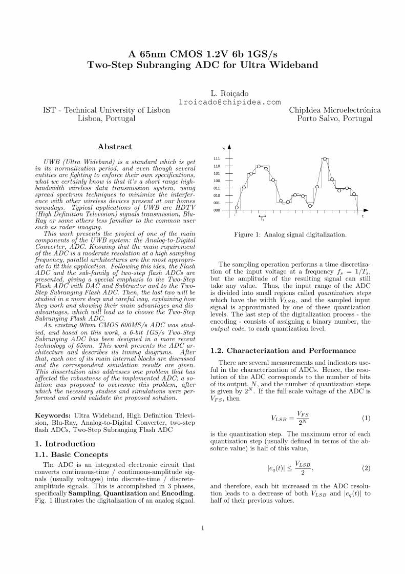
Figure 2: General architecture of a Flash ADC.
In an N -bit flash ADC there are 2N − 1 pre-amplifiers and latched comparators and one resistiveladder that divides the input range in 2N quantiza-tion levels. A sample-and-hold performs the samplingoperation and the pre-amplifiers subtract the sampledsignal from the reference voltages. If the differen-tial input voltage of the kth pre-amplifier is positive,(vIS − VREFk
) > 0, its differential output voltage willalso be positive and the latched comparator after it willregenerate the logic level high (the opposite occurs if(vIS−VREFk
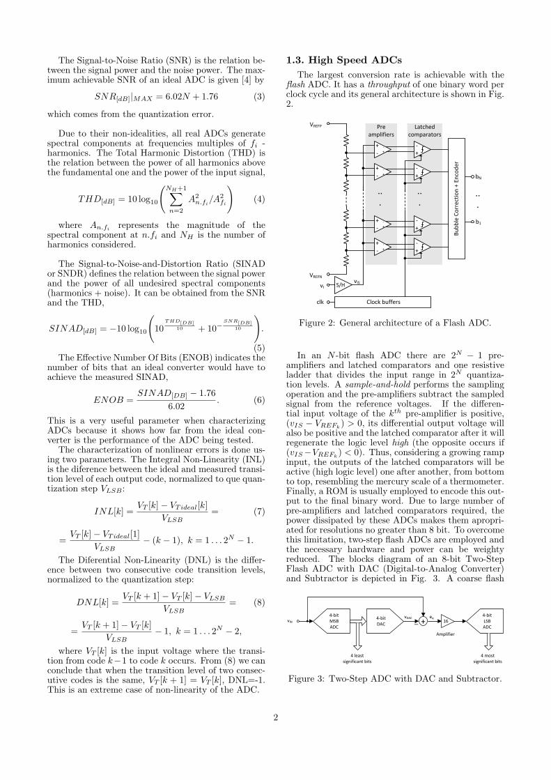
) < 0). Thus, considering a growing rampinput, the outputs of the latched comparators will beactive (high logic level) one after another, from bottomto top, resembling the mercury scale of a thermometer.Finally, a ROM is usually employed to encode this out-put to the final binary word. Due to large number ofpre-amplifiers and latched comparators required, thepower dissipated by these ADCs makes them apropri-ated for resolutions no greater than 8 bit. To overcomethis limitation, two-step flash ADCs are employed andthe necessary hardware and power can be weightyreduced. The blocks diagram of an 8-bit Two-StepFlash ADC with DAC (Digital-to-Analog Converter)and Subtractor is depicted in Fig. 3. A coarse flash
4‐bitMSBADC
4‐bitDAC +_ 16
4‐bitLSBADC
Amplifier
vIN
eqvDAC
4 least significant bits
4 mostsignificant bits
Figure 3: Two-Step ADC with DAC and Subtractor.
2
ADC obtains the 4 most significant bits (MSBs), whichthe DAC uses to generate a rough approximation ofthe input signal. The output of the DAC is, then, sub-tracted from the input signal yielding the residue, thatcorresponds to the error eq made in the coarse quanti-zation. This residue is multiplied by a factor of 16 andfinally, the fine ADC quantizes the amplified residueand obtains the 4 least significant bits (LSBs). Thisarchitecture requires only 2NMSB +2NLSB −2 = 30 pre-amplifiers and latched comparators, where the flashADC needed 255. However, this converter employs aDAC, a subtractor and an amplifier, whose linearity,gain error and settling speed are critical parametersthat limit the resolution and sampling frequency.
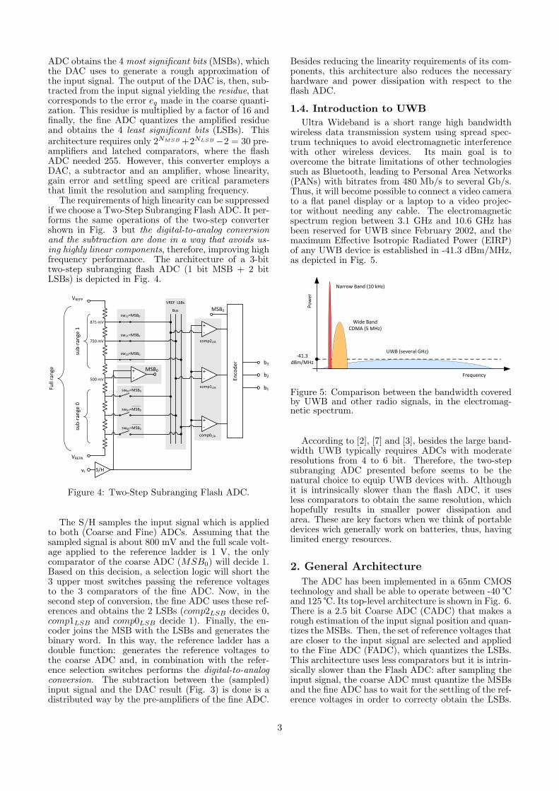
The requirements of high linearity can be suppressedif we choose a Two-Step Subranging Flash ADC. It per-forms the same operations of the two-step convertershown in Fig. 3 but the digital-to-analog conversionand the subtraction are done in a way that avoids us-ing highly linear components, therefore, improving highfrequency performance. The architecture of a 3-bittwo-step subranging flash ADC (1 bit MSB + 2 bitLSBs) is depicted in Fig. 4.
S/H
MSB0
VREFP
VREFN
vI
sw10=MSB0
sw11=MSB0
sw12=MSB0
sw00=MSB0
sw01=MSB0
sw02=MSB0
500 mV
sub‐
rang
e 0
750 mV
875 mV
sub‐
rang
e 1
Full
rang
e
Enco
der
b1
b2
b3
MSB0
+‐
+‐
+‐
+‐
comp0LSB
comp1LSB
comp2LSB
VREF LSBs
Bus
Figure 4: Two-Step Subranging Flash ADC.
The S/H samples the input signal which is appliedto both (Coarse and Fine) ADCs. Assuming that thesampled signal is about 800 mV and the full scale volt-age applied to the reference ladder is 1 V, the onlycomparator of the coarse ADC (MSB0) will decide 1.Based on this decision, a selection logic will short the3 upper most switches passing the reference voltagesto the 3 comparators of the fine ADC. Now, in thesecond step of conversion, the fine ADC uses these ref-erences and obtains the 2 LSBs (comp2LSB decides 0,comp1LSB and comp0LSB decide 1). Finally, the en-coder joins the MSB with the LSBs and generates thebinary word. In this way, the reference ladder has adouble function: generates the reference voltages tothe coarse ADC and, in combination with the refer-ence selection switches performs the digital-to-analogconversion. The subtraction between the (sampled)input signal and the DAC result (Fig. 3) is done is adistributed way by the pre-amplifiers of the fine ADC.
Besides reducing the linearity requirements of its com-ponents, this architecture also reduces the necessaryhardware and power dissipation with respect to theflash ADC.
1.4. Introduction to UWBUltra Wideband is a short range high bandwidth
wireless data transmission system using spread spec-trum techniques to avoid electromagnetic interferencewith other wireless devices. Its main goal is toovercome the bitrate limitations of other technologiessuch as Bluetooth, leading to Personal Area Networks(PANs) with bitrates from 480 Mb/s to several Gb/s.Thus, it will become possible to connect a video camerato a flat panel display or a laptop to a video projec-tor without needing any cable. The electromagneticspectrum region between 3.1 GHz and 10.6 GHz hasbeen reserved for UWB since February 2002, and themaximum Effective Isotropic Radiated Power (EIRP)of any UWB device is established in -41.3 dBm/MHz,as depicted in Fig. 5.
T1
Pow
er
UWB (several GHz)
Narrow Band (10 kHz)
Frequency
Wide BandCDMA (5 MHz)
‐41.3 dBm/MHz
Figure 5: Comparison between the bandwidth coveredby UWB and other radio signals, in the electromag-netic spectrum.
According to [2], [7] and [3], besides the large band-width UWB typically requires ADCs with moderateresolutions from 4 to 6 bit. Therefore, the two-stepsubranging ADC presented before seems to be thenatural choice to equip UWB devices with. Althoughit is intrinsically slower than the flash ADC, it usesless comparators to obtain the same resolution, whichhopefully results in smaller power dissipation andarea. These are key factors when we think of portabledevices wich generally work on batteries, thus, havinglimited energy resources.
2. General Architecture
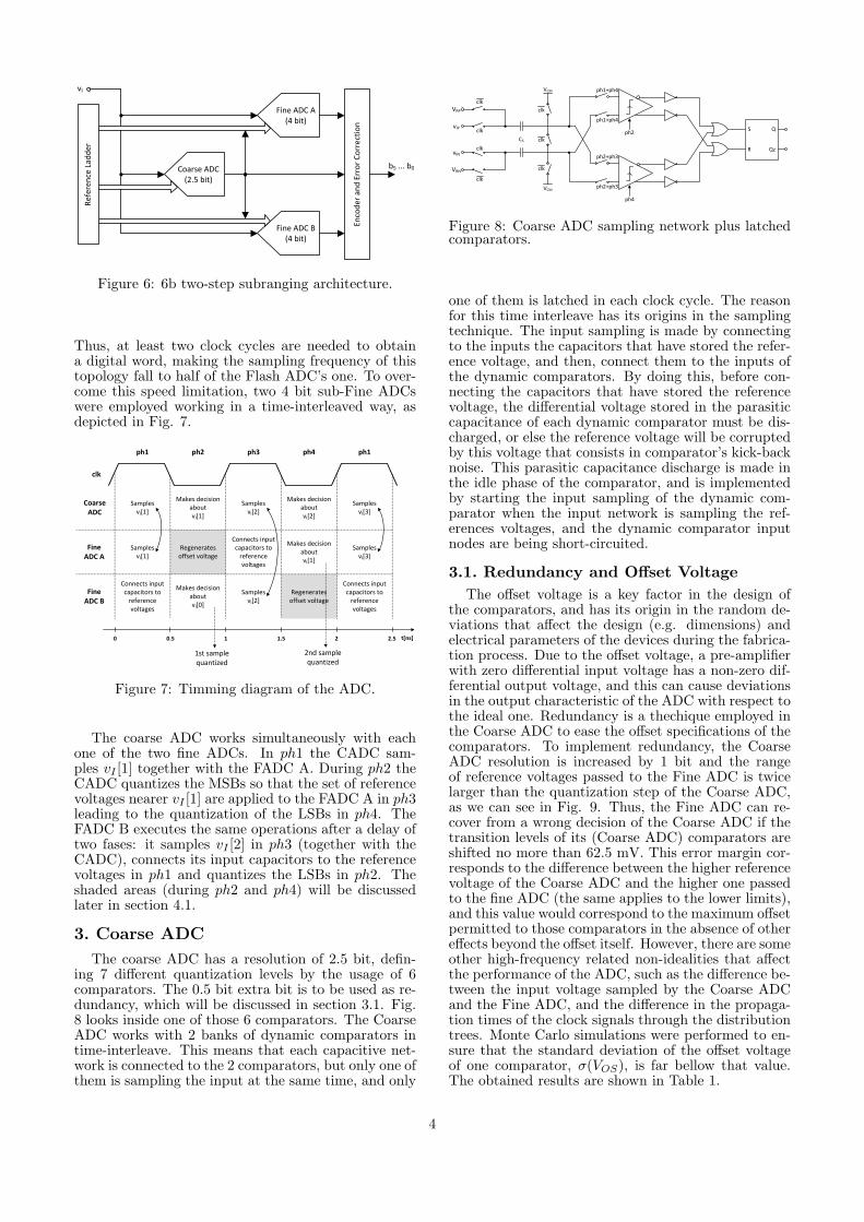
The ADC has been implemented in a 65nm CMOStechnology and shall be able to operate between -40 and 125 . Its top-level architecture is shown in Fig. 6.There is a 2.5 bit Coarse ADC (CADC) that makes arough estimation of the input signal position and quan-tizes the MSBs. Then, the set of reference voltages thatare closer to the input signal are selected and appliedto the Fine ADC (FADC), which quantizes the LSBs.This architecture uses less comparators but it is intrin-sically slower than the Flash ADC: after sampling theinput signal, the coarse ADC must quantize the MSBsand the fine ADC has to wait for the settling of the ref-erence voltages in order to correcty obtain the LSBs.
3
Refe
renc
e La
dder
Enco
der
and
Erro
r Co
rrec
tion
b5 ... b0
vI
Coarse ADC(2.5 bit)
Fine ADC B(4 bit)
Fine ADC A(4 bit)
Figure 6: 6b two-step subranging architecture.
Thus, at least two clock cycles are needed to obtaina digital word, making the sampling frequency of thistopology fall to half of the Flash ADC’s one. To over-come this speed limitation, two 4 bit sub-Fine ADCswere employed working in a time-interleaved way, asdepicted in Fig. 7.
SamplesvI[1]
SamplesvI[2]
SamplesvI[3]
SamplesvI[1]
SamplesvI[3]
Connects inputcapacitors to
reference voltages
Makes decisionaboutvI[0]
SamplesvI[2]
Regeneratesoffset voltage
CoarseADC
FineADC A
FineADC B
Connects inputcapacitors to
reference voltages
Connects inputcapacitors to
reference voltages
Regeneratesoffset voltage
Makes decisionaboutvI[1]
Makes decisionaboutvI[1]
Makes decisionaboutvI[2]
clk
ph1 ph2 ph3 ph4 ph1
t[ns]1.5 2 2.510.50
1st samplequantized
2nd samplequantized
Figure 7: Timming diagram of the ADC.
The coarse ADC works simultaneously with eachone of the two fine ADCs. In ph1 the CADC sam-ples vI [1] together with the FADC A. During ph2 theCADC quantizes the MSBs so that the set of referencevoltages nearer vI [1] are applied to the FADC A in ph3leading to the quantization of the LSBs in ph4. TheFADC B executes the same operations after a delay oftwo fases: it samples vI [2] in ph3 (together with theCADC), connects its input capacitors to the referencevoltages in ph1 and quantizes the LSBs in ph2. Theshaded areas (during ph2 and ph4) will be discussedlater in section 4.1.
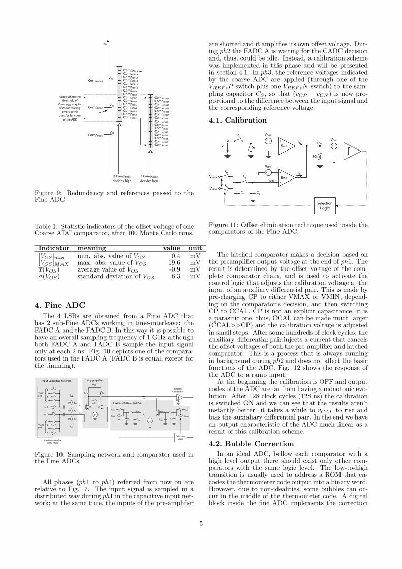
3. Coarse ADC
The coarse ADC has a resolution of 2.5 bit, defin-ing 7 different quantization levels by the usage of 6comparators. The 0.5 bit extra bit is to be used as re-dundancy, which will be discussed in section 3.1. Fig.8 looks inside one of those 6 comparators. The CoarseADC works with 2 banks of dynamic comparators intime-interleave. This means that each capacitive net-work is connected to the 2 comparators, but only one ofthem is sampling the input at the same time, and only
VCM
VCM
CS clk
clk
clk
clk
clk
VRP
vIP
vIN
VRN
ph2+ph3
ph2+ph3
ph1+ph4
ph1+ph4
clk
clk
S
R
Q
Qz
ph4
ph2
Figure 8: Coarse ADC sampling network plus latchedcomparators.
one of them is latched in each clock cycle. The reasonfor this time interleave has its origins in the samplingtechnique. The input sampling is made by connectingto the inputs the capacitors that have stored the refer-ence voltage, and then, connect them to the inputs ofthe dynamic comparators. By doing this, before con-necting the capacitors that have stored the referencevoltage, the differential voltage stored in the parasiticcapacitance of each dynamic comparator must be dis-charged, or else the reference voltage will be corruptedby this voltage that consists in comparator’s kick-backnoise. This parasitic capacitance discharge is made inthe idle phase of the comparator, and is implementedby starting the input sampling of the dynamic com-parator when the input network is sampling the ref-erences voltages, and the dynamic comparator inputnodes are being short-circuited.
3.1. Redundancy and Offset VoltageThe offset voltage is a key factor in the design of
the comparators, and has its origin in the random de-viations that affect the design (e.g. dimensions) andelectrical parameters of the devices during the fabrica-tion process. Due to the offset voltage, a pre-amplifierwith zero differential input voltage has a non-zero dif-ferential output voltage, and this can cause deviationsin the output characteristic of the ADC with respect tothe ideal one. Redundancy is a thechique employed inthe Coarse ADC to ease the offset specifications of thecomparators. To implement redundancy, the CoarseADC resolution is increased by 1 bit and the rangeof reference voltages passed to the Fine ADC is twicelarger than the quantization step of the Coarse ADC,as we can see in Fig. 9. Thus, the Fine ADC can re-cover from a wrong decision of the Coarse ADC if thetransition levels of its (Coarse ADC) comparators areshifted no more than 62.5 mV. This error margin cor-responds to the difference between the higher referencevoltage of the Coarse ADC and the higher one passedto the fine ADC (the same applies to the lower limits),and this value would correspond to the maximum offsetpermitted to those comparators in the absence of othereffects beyond the offset itself. However, there are someother high-frequency related non-idealities that affectthe performance of the ADC, such as the difference be-tween the input voltage sampled by the Coarse ADCand the Fine ADC, and the difference in the propaga-tion times of the clock signals through the distributiontrees. Monte Carlo simulations were performed to en-sure that the standard deviation of the offset voltageof one comparator, σ(VOS), is far bellow that value.The obtained results are shown in Table 1.
4
CompMSB3
CompMSB2
CompMSB1
VR3
VR2
VR1
vI
if CompMSB2
decides highif CompMSB2
decides low
CompLSB15CompLSB14
CompLSB12CompLSB11CompLSB10CompLSB9CompLSB8CompLSB7CompLSB6CompLSB5CompLSB4CompLSB3CompLSB2CompLSB1
CompLSB13
CompLSB8
CompLSB15CompLSB14CompLSB13CompLSB12CompLSB11CompLSB10CompLSB9
CompLSB7CompLSB6CompLSB5CompLSB4CompLSB3CompLSB2CompLSB1
Range where the threshold of
CompMSB2 may lie without causing
errors in the transfer function
of the ADC
vIN
Figure 9: Redundancy and references passed to theFine ADC.
Table 1: Statistic indicators of the offset voltage of oneCoarse ADC comparator, after 100 Monte Carlo runs.
Indicator meaning value unit|VOS |min min. abs. value of VOS 0.4 mV|VOS |MAX max. abs. value of VOS 19.6 mVx(VOS) average value of VOS -0.9 mVσ(VOS) standard deviation of VOS 6.3 mV
4. Fine ADC
The 4 LSBs are obtained from a Fine ADC thathas 2 sub-Fine ADCs working in time-interleave: theFADC A and the FADC B. In this way it is possible tohave an overall sampling frequency of 1 GHz althoughboth FADC A and FADC B sample the input signalonly at each 2 ns. Fig. 10 depicts one of the compara-tors used in the FADC A (FADC B is equal, except forthe timming).
VCM
VCM
CS ph1ph1
ph1vIP
vIN
ph4
ph4
VMAX
VMIN
CP CCAL
VCALP
clk
VDD
R0 R0
VMIN
VMAX
CPCCAL
VCALN
SelectionLogic
clk
LatchedComparator
Pre‐amplifierInput Capacitive Network
VREFsP ph3
VREFsN ph3
Auxiliary Differential PairS1a
S1b
S2
vCP
vCN
Selection accordingto the MSBs
IB
M2M1
VMAX
VMIN
CP CS
vCAL
SelectionLogic
+ -
gm2
+
-S3
S2
+ -
gm1
+
-
VOS1
VOS2
S1
S4
S5
+ -
VOSl
R0
vI
i2
i1 vOA
Figure 10: Sampling network and comparator used inthe Fine ADCs.
All phases (ph1 to ph4) referred from now on arerelative to Fig. 7. The input signal is sampled in adistributed way during ph1 in the capacitive input net-work; at the same time, the inputs of the pre-amplifier
are shorted and it amplifies its own offset voltage. Dur-ing ph2 the FADC A is waiting for the CADC decisionand, thus, could be idle. Instead, a calibration schemewas implemented in this phase and will be presentedin section 4.1. In ph3, the reference voltages indicatedby the coarse ADC are applied (through one of theVREFsP switch plus one VREFsN switch) to the sam-pling capacitor CS , so that (vCP − vCN ) is now pro-portional to the difference between the input signal andthe corresponding reference voltage.
4.1. Calibration
VCM
VCM
CS ph1ph1
ph1vIP
vIN
ph4
ph4
VMAX
VMIN
CP CCAL
VCALP
clk
VDD
R0 R0
VMIN
VMAX
CPCCAL
VCALN
SelectionLogic
clk
LatchedComparator
Pre‐amplifierInput Capacitive Network
VREFsP ph3
VREFsN ph3
Auxiliary Differential PairS1a
S1b
S2
vCP
vCN
Selection accordingto the MSBs
IB
M2M1
VMAX
VMIN
CP CS
vCAL
SelectionLogic
+ -
gm2
+
-S3
S2
+ -
gm1
+
-
VOS1
VOS2
S1
S4
S5
+ -
VOSl
R0
vI
i2
i1 vOA
Figure 11: Offset elimination technique used inside thecomparators of the Fine ADC.
The latched comparator makes a decision based onthe preamplifier output voltage at the end of ph1. Theresult is determined by the offset voltage of the com-plete comparator chain, and is used to activate thecontrol logic that adjusts the calibration voltage at theinput of an auxiliary differential pair. This is made bypre-charging CP to either VMAX or VMIN, depend-ing on the comparator’s decision, and then switchingCP to CCAL. CP is not an explicit capacitance, it isa parasitic one, thus, CCAL can be made much larger(CCAL>>CP) and the calibration voltage is adjustedin small steps. After some hundreds of clock cycles, theauxiliary differential pair injects a current that cancelsthe offset voltages of both the pre-amplifier and latchedcomparator. This is a process that is always runningin background during ph2 and does not affect the basicfunctions of the ADC. Fig. 12 shows the response ofthe ADC to a ramp input.
At the beginning the calibration is OFF and outputcodes of the ADC are far from having a monotonic evo-lution. After 128 clock cycles (128 ns) the calibrationis switched ON and we can see that the results aren’tinstantly better: it takes a while to vCAL to rise andbias the auxialiary differential pair. In the end we havean output characteristic of the ADC much linear as aresult of this calibration scheme.
4.2. Bubble CorrectionIn an ideal ADC, bellow each comparator with a
high level output there should exist only other com-parators with the same logic level. The low-to-hightransition is usually used to address a ROM that en-codes the thermometer code output into a binary word.However, due to non-idealities, some bubbles can oc-cur in the middle of the thermometer code. A digitalblock inside the fine ADC implements the correction
5
0 50 100 150 200 250 300 350 400 450 5000
8
16
24
32
40
48
56
64
Clock Cycles
Outpu
t Cod
e
calibration OFF calibration ON
Figure 12: Output codes of the ADC (ramp input)with calibration OFF (until 128 ns) and then ON.
scheme presented in [8], and we can check its validnessin the simulation depicted in Fig. 13, where 3 errorswere present at the input of the ADC.
printed Mon Oct 8 2007 22:45:43 by lroicado on pc-lroicado Sandwork Design, Inc. (c) 2000-2006
0
0
2n
2n
4n
4n
6n
6n
8n
8n
10n
10n
12n
12n
14n
14n
16n
16n
18n
18n
(lin)
00.61.2vo
lt (li
n)
input15 0
00.61.2vo
lt (li
n)
input14 0
00.61.2vo
lt (li
n)
input13 0
00.61.2vo
lt (li
n)
input12 0
00.61.2vo
lt (li
n)
input11 0
00.61.2vo
lt (li
n)
input10 0
00.61.2vo
lt (li
n)
input9 0
00.61.2vo
lt (li
n)
input8 0
00.61.2vo
lt (li
n)
input7 0
00.61.2vo
lt (li
n)
input6 0
00.61.2vo
lt (li
n)
input5 0
00.61.2vo
lt (li
n)
input4 0
00.61.2vo
lt (li
n)
input3 1.2
00.61.2vo
lt (li
n)
input2 0
00.61.2vo
lt (li
n)
input1 1.2
00.61.2vo
lt (li
n)
input0 1.2
00.61.2 (
lin)
[lsb3] 6.7u
00.61.2vo
lt (li
n)
[lsb2] 6.03u
00.61.2vo
lt (li
n)
[lsb1] 1.2
00.61.2vo
lt (li
n)
[lsb0] 1.2
1:4.7n
-4n-9.03n
2:8.7n 3:13.7n
Figure 13: Simulation of the bubble correction logic.
Each comparator changes its decision if it disagreeswith both neighbours. The equation that representsthis correction scheme is
CN∗ = C(N−1)·CN + CN ·C(N+1)·+C(N−1)·C(N+1),(9)
where CN is the output of the N th comparator withoutcorrection and CN∗ represents the same output aftercorrection. Taking the 2nd error applied to the inputof this logic block, the 7th comparator which is respon-sible for the bubble at 8.7 ns will change its decisionfrom 0 to 1, and the corresponding corrected binaryword is 9, as indicated by the output signals lsb0 tolsb3.
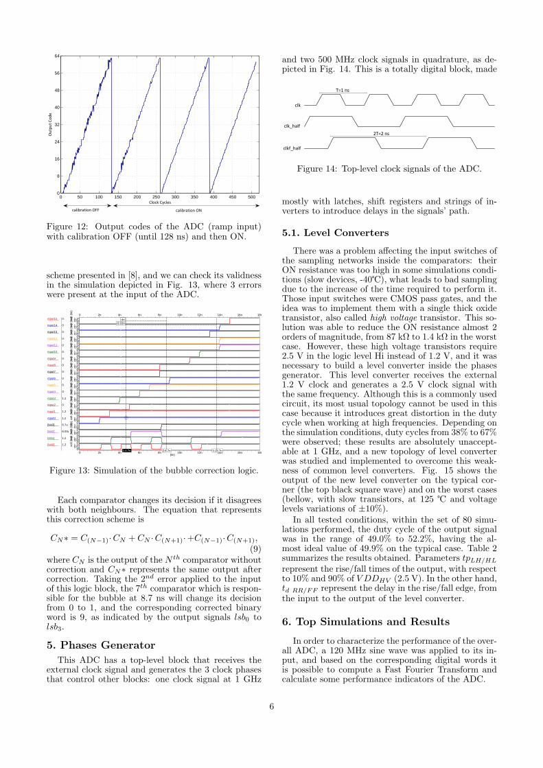
5. Phases Generator
This ADC has a top-level block that receives theexternal clock signal and generates the 3 clock phasesthat control other blocks: one clock signal at 1 GHz
and two 500 MHz clock signals in quadrature, as de-picted in Fig. 14. This is a totally digital block, made
D
Clk
Q
QzClk
D
Clk
Q
QzClk
D
Clk
Q
QzClk
LSB<3:0>
D
Clk
Q
QzClk
MSB<2:0>
3-bit Σ
MSB<2:0>d
LSB<3>d
clk
clk_half
clkf_half
2T=2 ns
T=1 ns
Figure 14: Top-level clock signals of the ADC.
mostly with latches, shift registers and strings of in-verters to introduce delays in the signals’ path.
5.1. Level Converters
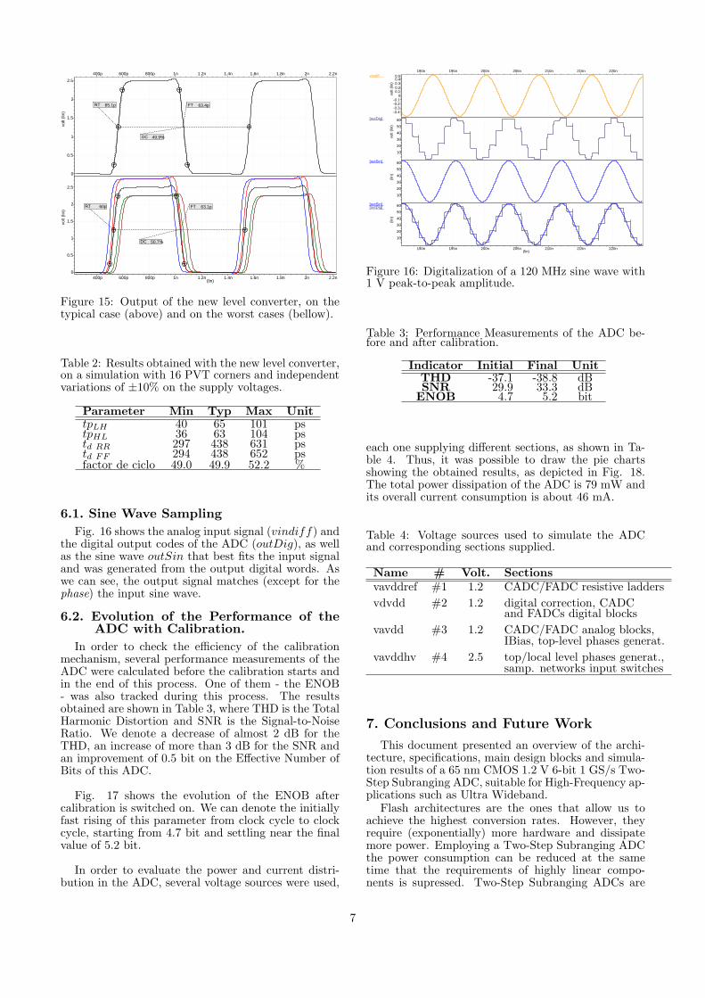
There was a problem affecting the input switches ofthe sampling networks inside the comparators: theirON resistance was too high in some simulations condi-tions (slow devices, -40), what leads to bad samplingdue to the increase of the time required to perform it.Those input switches were CMOS pass gates, and theidea was to implement them with a single thick oxidetransistor, also called high voltage transistor. This so-lution was able to reduce the ON resistance almost 2orders of magnitude, from 87 kΩ to 1.4 kΩ in the worstcase. However, these high voltage transistors require2.5 V in the logic level Hi instead of 1.2 V, and it wasnecessary to build a level converter inside the phasesgenerator. This level converter receives the external1.2 V clock and generates a 2.5 V clock signal withthe same frequency. Although this is a commonly usedcircuit, its most usual topology cannot be used in thiscase because it introduces great distortion in the dutycycle when working at high frequencies. Depending onthe simulation conditions, duty cycles from 38% to 67%were observed; these results are absolutely unaccept-able at 1 GHz, and a new topology of level converterwas studied and implemented to overcome this weak-ness of common level converters. Fig. 15 shows theoutput of the new level converter on the typical cor-ner (the top black square wave) and on the worst cases(bellow, with slow transistors, at 125 and voltagelevels variations of ±10%).
In all tested conditions, within the set of 80 simu-lations performed, the duty cycle of the output signalwas in the range of 49.0% to 52.2%, having the al-most ideal value of 49.9% on the typical case. Table 2summarizes the results obtained. Parameters tpLH/HL
represent the rise/fall times of the output, with respectto 10% and 90% of V DDHV (2.5 V). In the other hand,td RR/FF represent the delay in the rise/fall edge, fromthe input to the output of the level converter.
6. Top Simulations and Results
In order to characterize the performance of the over-all ADC, a 120 MHz sine wave was applied to its in-put, and based on the corresponding digital words itis possible to compute a Fast Fourier Transform andcalculate some performance indicators of the ADC.
6
printed Fri Sep 21 2007 16:09:15 by lroicado on pc-lroicado Sandwork Design, Inc. (c) 2000-2006
400p
400p
600p
600p
800p
800p
1n
1n
1.2n
1.2n
1.4n
1.4n
1.6n
1.6n
1.8n
1.8n
2n
2n
2.2n
2.2n
(lin)
0
0.5
1
1.5
2
2.5
volt
(lin)
ph:avddk=1:avddhvk=1
0
0.5
1
1.5
2
2.5
volt
(lin)
ph:avddk=1:avddhvk=1ph:avddk=0.9:avddhvk=1.1ph:avddk=1.1:avddhvk=0.9ph:avddk=0.9:avddhvk=0.9ph:avddk=1.1:avddhvk=1.1
DC 50.7%
RT 65.1p FT 63.4p
RT 60p FT 63.1p
DC 49.9%
DC 50.7%
RT 65.1p FT 63.4p
RT 60p FT 63.1p
DC 49.9%
Figure 15: Output of the new level converter, on thetypical case (above) and on the worst cases (bellow).
Table 2: Results obtained with the new level converter,on a simulation with 16 PVT corners and independentvariations of ±10% on the supply voltages.
Parameter Min Typ Max UnittpLH 40 65 101 pstpHL 36 63 104 pstd RR 297 438 631 pstd FF 294 438 652 psfactor de ciclo 49.0 49.9 52.2 %
6.1. Sine Wave SamplingFig. 16 shows the analog input signal (vindiff) and
the digital output codes of the ADC (outDig), as wellas the sine wave outSin that best fits the input signaland was generated from the output digital words. Aswe can see, the output signal matches (except for thephase) the input sine wave.
6.2. Evolution of the Performance of theADC with Calibration.
In order to check the efficiency of the calibrationmechanism, several performance measurements of theADC were calculated before the calibration starts andin the end of this process. One of them - the ENOB- was also tracked during this process. The resultsobtained are shown in Table 3, where THD is the TotalHarmonic Distortion and SNR is the Signal-to-NoiseRatio. We denote a decrease of almost 2 dB for theTHD, an increase of more than 3 dB for the SNR andan improvement of 0.5 bit on the Effective Number ofBits of this ADC.
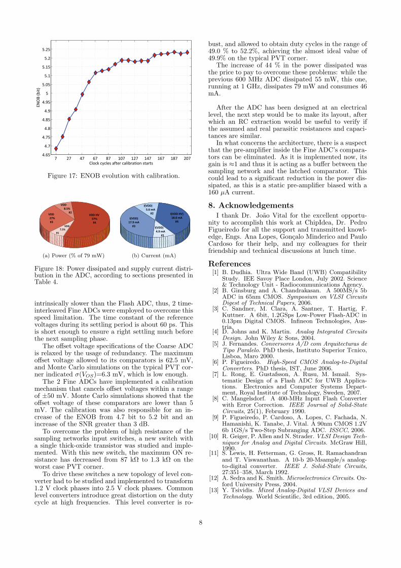
Fig. 17 shows the evolution of the ENOB aftercalibration is switched on. We can denote the initiallyfast rising of this parameter from clock cycle to clockcycle, starting from 4.7 bit and settling near the finalvalue of 5.2 bit.
In order to evaluate the power and current distri-bution in the ADC, several voltage sources were used,
printed Wed Oct 10 2007 11:48:23 by lroicado on pc-lroicado Sandwork Design, Inc. (c) 2000-2006
190n
190n
195n
195n
200n
200n
205n
205n
210n
210n
215n
215n
220n
220n
(lin)
-0.4-0.3-0.2-0.1
00.10.20.30.40.5
volt
(lin)
vindiff
10
20
30
40
50
60
volt
(lin)
[outDig]
10
20
30
40
50
60
(lin
)
[outSin]
10
20
30
40
50
60
(lin
)
[outSin][outDig]
Figure 16: Digitalization of a 120 MHz sine wave with1 V peak-to-peak amplitude.
Table 3: Performance Measurements of the ADC be-fore and after calibration.
Indicator Initial Final UnitTHD -37.1 -38.8 dBSNR 29.9 33.3 dB
ENOB 4.7 5.2 bit
each one supplying different sections, as shown in Ta-ble 4. Thus, it was possible to draw the pie chartsshowing the obtained results, as depicted in Fig. 18.The total power dissipation of the ADC is 79 mW andits overall current consumption is about 46 mA.
Table 4: Voltage sources used to simulate the ADCand corresponding sections supplied.
Name # Volt. Sectionsvavddref #1 1.2 CADC/FADC resistive laddersvdvdd #2 1.2 digital correction, CADC
and FADCs digital blocksvavdd #3 1.2 CADC/FADC analog blocks,
IBias, top-level phases generat.vavddhv #4 2.5 top/local level phases generat.,
samp. networks input switches
7. Conclusions and Future Work
This document presented an overview of the archi-tecture, specifications, main design blocks and simula-tion results of a 65 nm CMOS 1.2 V 6-bit 1 GS/s Two-Step Subranging ADC, suitable for High-Frequency ap-plications such as Ultra Wideband.
Flash architectures are the ones that allow us toachieve the highest conversion rates. However, theyrequire (exponentially) more hardware and dissipatemore power. Employing a Two-Step Subranging ADCthe power consumption can be reduced at the sametime that the requirements of highly linear compo-nents is supressed. Two-Step Subranging ADCs are
7
7 27 47 67 87 107 127 147 167 187 207
4.7
4.75
4.8
4.9
5
4.65
4.85
4.95
5.05
5.15
5.25
5.1
5.2
Clock cycles after calibration starts
ENOB (bit)
Figure 17: ENOB evolution with calibration.
VDD HV 57%
#4
VDD 8.5% #2
VDD 7.5%
#1
VDD 27%
#3
(a) Power (% of 79 mW)
I(VDD HV)18.0 mA
#4
I(VDD) 4.9 mA #1
I(VDD) 5.6 mA #2
I(VDD)17.9 mA
#3
(b) Current (mA)
Figure 18: Power dissipated and supply current distri-bution in the ADC, according to sections presented inTable 4.
intrinsically slower than the Flash ADC, thus, 2 time-interleaved Fine ADCs were employed to overcome thisspeed limitation. The time constant of the referencevoltages during its settling period is about 60 ps. Thisis short enough to ensure a right settling much beforethe next sampling phase.
The offset voltage specifications of the Coarse ADCis relaxed by the usage of redundancy. The maximumoffset voltage allowed to its comparators is 62.5 mV,and Monte Carlo simulations on the typical PVT cor-ner indicated σ(VOS)=6.3 mV, which is low enough.
The 2 Fine ADCs have implemented a calibrationmechanism that cancels offset voltages within a rangeof ±50 mV. Monte Carlo simulations showed that theoffset voltage of these comparators are lower than 5mV. The calibration was also responsible for an in-crease of the ENOB from 4.7 bit to 5.2 bit and anincrease of the SNR greater than 3 dB.
To overcome the problem of high resistance of thesampling networks input switches, a new switch witha single thick-oxide transistor was studied and imple-mented. With this new switch, the maximum ON re-sistance has decreased from 87 kΩ to 1.3 kΩ on theworst case PVT corner.
To drive these switches a new topology of level con-verter had to be studied and implemented to transform1.2 V clock phases into 2.5 V clock phases. Commonlevel converters introduce great distortion on the dutycycle at high frequencies. This level converter is ro-
bust, and allowed to obtain duty cycles in the range of49.0 % to 52.2%, achieving the almost ideal value of49.9% on the typical PVT corner.
The increase of 44 % in the power dissipated wasthe price to pay to overcome these problems: while theprevious 600 MHz ADC dissipated 55 mW, this one,running at 1 GHz, dissipates 79 mW and consumes 46mA.
After the ADC has been designed at an electricallevel, the next step would be to make its layout, afterwhich an RC extraction would be useful to verify ifthe assumed and real parasitic resistances and capaci-tances are similar.
In what concerns the architecture, there is a suspectthat the pre-amplifier inside the Fine ADC’s compara-tors can be eliminated. As it is implemented now, itsgain is ≈1 and thus it is acting as a buffer between thesampling network and the latched comparator. Thiscould lead to a significant reduction in the power dis-sipated, as this is a static pre-amplifier biased with a160 µA current.
8. AcknowledgementsI thank Dr. Joao Vital for the excellent opportu-
nity to accomplish this work at ChipIdea, Dr. PedroFigueiredo for all the support and transmitted knowl-edge, Engs. Ana Lopes, Goncalo Minderico and PauloCardoso for their help, and my colleagues for theirfriendship and technical discussions at lunch time.
References[1] B. Dudhia. Ultra Wide Band (UWB) Compatibility
Study. IEE Savoy Place London, July 2002. Science& Technology Unit - Radiocommunications Agency.
[2] B. Ginsburg and A. Chandrakasan. A 500MS/s 5bADC in 65nm CMOS. Symposium on VLSI CircuitsDigest of Technical Papers, 2006.
[3] C. Sandner, M. Clara, A. Santner, T. Hartig, F.Kuttner. A 6bit, 1.2GSps Low-Power Flash-ADC in0.13pm Digital CMOS. Infineon Technologies, Aus-tria.
[4] D. Johns and K. Martin. Analog Integrated CircuitsDesign. John Wiley & Sons, 2004.
[5] J. Fernandes. Conversores A/D com Arquitecturas deTipo Paralelo. PhD thesis, Instituto Superior Tcnico,Lisboa, Maro 2000.
[6] P. Figueiredo. High-Speed CMOS Analog-to-DigitalConverters. PhD thesis, IST, June 2006.
[7] L. Rong, E. Gustafsson, A. Rusu, M. Ismail. Sys-tematic Design of a Flash ADC for UWB Applica-tions. Electronics and Computer Systems Depart-ment, Royal Institute of Technology, Sweden, 2007.
[8] C. Mangelsdorf. A 400-MHz Input Flash Converterwith Error Correction. IEEE Journal of Solid-StateCircuits, 25(1), February 1990.
[9] P. Figueiredo, P. Cardoso, A. Lopes, C. Fachada, N.Hamanishi, K. Tanabe, J. Vital. A 90nm CMOS 1.2V6b 1GS/s Two-Step Subranging ADC. ISSCC, 2006.
[10] R. Geiger, P. Allen and N. Strader. VLSI Design Tech-niques for Analog and Digital Circuits. McGraw Hill,1990.
[11] S. Lewis, H. Fetterman, G. Gross, R. Ramachandranand T. Viswanathan. A 10-b 20-Msample/s analog-to-digital converter. IEEE J. Solid-State Circuits,27:351–358, March 1992.
[12] A. Sedra and K. Smith. Microelectronics Circuits. Ox-ford University Press, 2004.
[13] Y. Tsividis. Mixed Analog-Digital VLSI Devices andTechnology. World Scientific, 3rd edition, 2005.
8